ors based on two dimensionalgraphene and graphene/semiconductorheterojunctions
Zhongcheng Zhu,†a Imran Murtaza,†bc Hong Meng*ab and Wei Huangb
During the past few years, two-dimensional (2D) layered materials have emerged as the most fundamental
building blocks of a wide variety of optoelectronic devices. The weak van der Waals (vdW) interlayer forces
allow the 2D monolayers to isolate and restack into arbitrary stacking heterojunctions. The recently
developed chemical vapor deposition (CVD) technique shows great promise for the production of large
domain building blocks of 2D heterostructures with vertical and lateral stacking and much better device
performance. This review is the first of its kind to discuss the research progress of flexible FETs based on
graphene/semiconductor heterostructures, in which graphene acts as both electrode and semiconductor
material.
1. Introduction
Two-dimensional (2D) materials, such as nano-lms, super-lattices and quantum wells, refer to the materials in which thefree movement (plane motion) of electrons takes place only inthe two dimensional non-nanoscale. Graphene is the mostsignicant among all the 2D materials proposed up till now1
and has single (or several) atomic layer thickness. Beyond gra-phene, 2D materials also include transition metal oxides (e.g.MnO2, ZnO), transition metal carbides and/or carbonitrides(MXene), transition metal chalcogenides (e.g. MoS2), hexagonalboron nitride (h-BN), topological insulators (e.g. Bi2Se3, Sb2Te3),silicene, germanene, black phosphorus (BP) and so on(Fig. 1).2–5 2D materials as promising building blocks for novelnanoelectronics include semiconductors, insulators, trans-parent conductors and transducers,6–8 because amongst otherconsiderations, these atomic sheets afford the ultimate thick-ness and scalability, which is desired in a variety of essentialmaterial categories. 2D semiconductors exhibit high carriermobility, high on–off current ratio and excellent bendabilitythat suit for future low-power consumption and exible elec-tronics.9–12 These materials are laterally composed of strongcovalent bonds, which provide great in-plane stability. On theother hand, the weak van der Waals (vdW) interlayer forcesallow us to isolate 2Dmonolayer and restack them into arbitrarystacking heterojunctions without the need to consider the
atomic commensurability in contrast to their bulk counterparts.van der Waals (vdW)-bonded layered materials offer greatvariety in both structural and electronic properties, opening upnew avenues for scientic research to obtain better devicedesign and desired device functionalities by assembling heter-ostructures based on distinct 2D layers. Although, all-2D vdWheterostructures offer unique properties and functionalitiescompared with conventional devices, it still remains a challengeto produce entire families of 2D materials and their hetero-structures over large areas with high electronic quality.Furthermore, control of doping type, carrier concentration andstoichiometry is quiet difficult for most 2D materials, limitingthe scope and progress of all-2D vdW heterostructures.13
Graphene is the rst truly 2D crystalline material, which iscomposed of periodic honeycomb lattice formed by sp2 hybridorbitals of covalently bonded carbon atoms (Fig. 1b and c).12,14–17
The p orbital of coplanar carbon atoms overlap each other andform large conjugated p bonds. There is a freely moving elec-tron at each grid point, which endow graphene to have superhigh electron mobility (2 � 105 cm2 V�1 s�1) at low temperature(�5 K).1,18 Graphene is theoretically considered as zero bandgapsemiconductor and the electronic conduction velocity andtheoretical resistivity of graphene are 8� 105 m s�1 (ref. 19) and10�6 U cm�1,20 respectively. Excellent electrical property ofgraphene favors the development of graphene based eld effecttransistors21 and the supercapacitors.22 In addition, graphenehas high optical transparency23 and has broad applications inthe transparent conductive thin lm solar cells, photon detec-tors and so on,24–28 due to its unique optical properties. Inaddition, graphene also exhibits ultrahigh mechanical strength(1.0 TPa),29 exceptional thermal conductivity (5000 W m�1
K�1),30 half-integer quantum Hall effect at room temperature,31
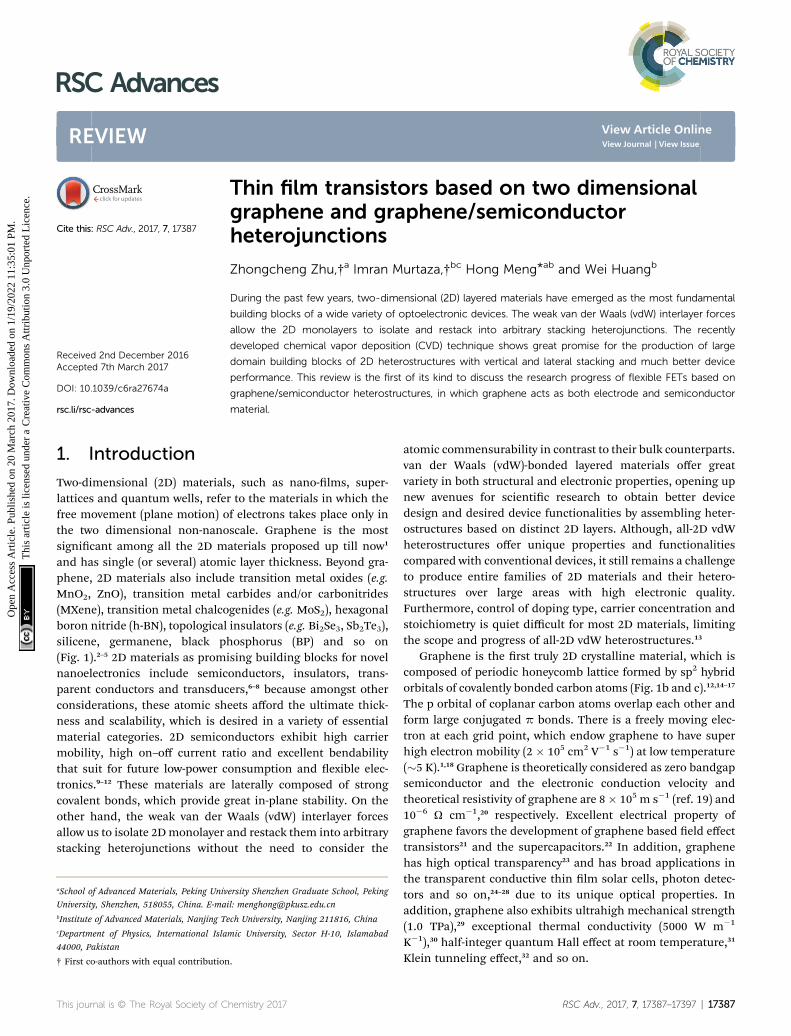
Fig. 1 (a) Schematic illustration of different kinds of typical ultrathin 2D nanomaterials, such as graphene, h-BN, TMDs, MOFs, COFs, MXenes,LDHs, oxides, metals, and BP. Reprinted with permission from ref. 3. Copyright 2015 ACS Publications. (b) Charge carriers in graphene are calledmassless Dirac fermions and are described by a 2D analog of the Dirac equation, with the Fermi velocity vFz 1� 106 m s�1 playing the role of thespeed of light and a 2D pseudospin ~s describing two sublattices of the honeycomb lattice. Reprinted with permission from ref. 12. Copyright2009 AAAS. (c) TEM image, reprintedwith permission from ref. 13. Copyright 2011 ACS Publications. (d) Atomic structure of graphene obtained byDFT calculation. Reprinted with permission from ref. 14. Copyright 2008 ACS Publications. (e) vdW forces in a 2D layered structure. Reprintedfrom http://bbc.co.uk.
RSC Advances Review
Ope
n A
cces
s A
rtic
le. P
ublis
hed
on 2
0 M
arch
201
7. D
ownl
oade
d on
1/1
9/20
22 1
1:35
:01
PM.
Thi
s ar
ticle
is li
cens
ed u
nder
a C
reat
ive
Com
mon
s A
ttrib
utio
n 3.
0 U
npor
ted
Lic
ence
.View Article Online
Transistors are the central device building blocks of allmodern electronic systems. The rst thin lm transistors (TFTs)can be dated back to 1962,33 which used vacuum evaporationtechnique along with shadow masks to deposit gold electrodes,an n-type polycrystalline cadmium sulde (CdS) semiconductorchannel and a Si monoxide gate insulator on a glass substrate.The integration of TFTs on exible substrates is of considerableinterest for diverse applications including electronic-paper,wearable display and articial skin, and can enable a newgeneration of exible, wearable and disposable electronics.34–37
The major challenges for the realization of high performanceelectronics on exible substrates are the difficulties in achievingTFTs with a high carrier mobility, high on/off ratio, low oper-ating voltage and using a low temperature-compatible fabrica-tion process.
The highest carrier mobility, excellent optical transparency,high mechanical strength as well as atomic thickness of gra-phene layers make it extremely useful for exible FET applica-tion. Fabrication of FETs using 2D graphene crystals as an activecomponent can signicantly contribute in the evolution of nextgeneration exible thin lm electronic devices and there havebeen quite a few reviews summarizing the graphene-based TFTsand their applications.38–45 Keeping in view the high demand ofgraphene based exible electronics, in this review, we summa-rize recent development of exible FETs based on grapheneand/or graphene/semiconductor heterojunctions, consistent
17388 | RSC Adv., 2017, 7, 17387–17397
with the role of graphene as channel layer and/or electrodes inFETs.
2. Graphene acting as channelmaterial in thin film transistors
For eld-effect transistors (FETs), the level of its carrier mobilityoen determine the level of some other important performanceparameters, such as current density, energy efficiency, switch-ing delay, and so on. High mobility is benecial to realize themaximum static control,7 optical transparency,46 sensitivity47
and exibility,48,49 and broaden the application elds of TFTs. Inthis regard, graphene is one of the best choice for transparentconductive thin lms in FETs, due to its excellent electronic,mechanical, optical properties and good stability as mentionedabove.18,23,29
Graphene transparent conductive thin lms have been usuallyused as the conducting channel layer for graphene-based eldeffect transistors (GFETs). Themain opportunities for graphene inboth high-performance and low-power applications stem from theatomic thinness achievable in graphene-based devices, which leadto an almost perfect control of the channel potential. Veryrecently, Johari et al.50 have reviewed the electrical performance ofGFETs using various architectures and different geometries ofgraphene conducting channel layer. Graphene has great advan-tage for its use in exible electronics but at the same time it needs
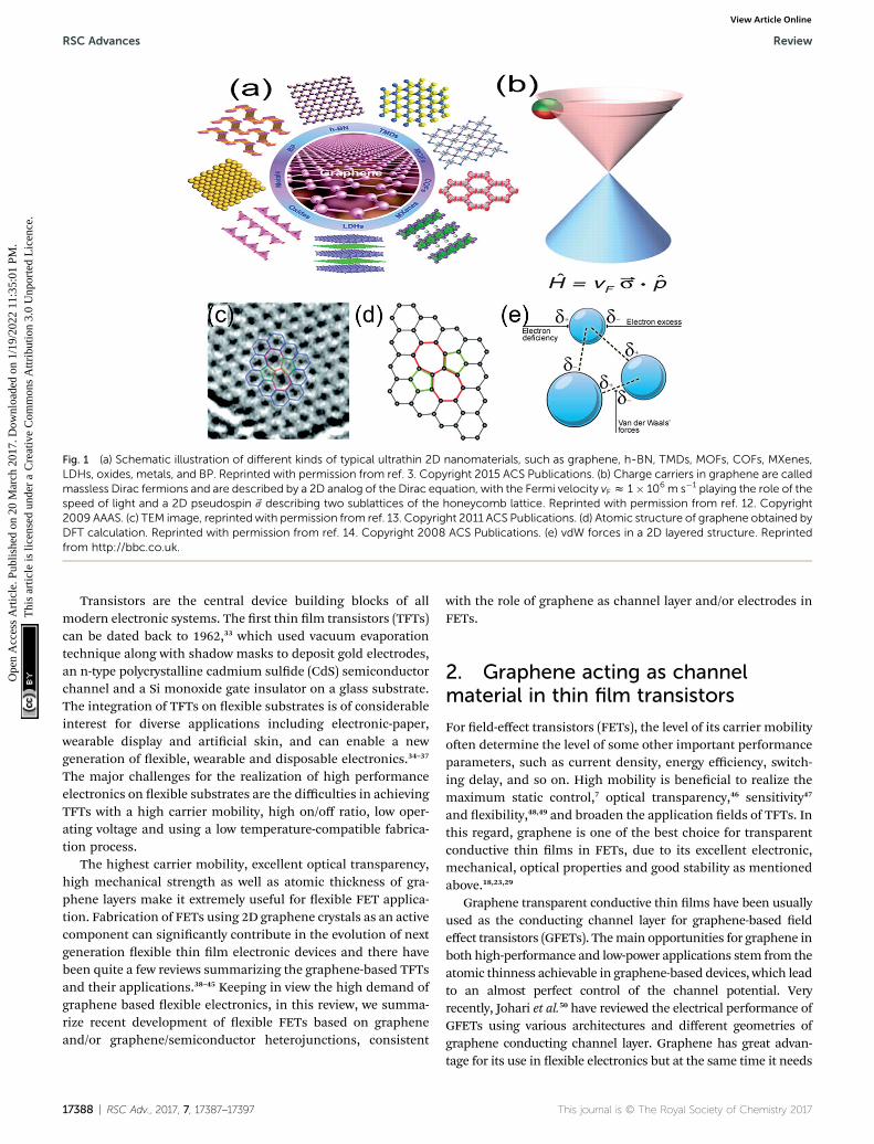
Fig. 2 Schematic 2D heterostructures based on van der Waals inter-layer force. Reprinted with permission from ref. 67. Copyright 2013Nature Publishing Group.
Review RSC Advances
Ope
n A
cces
s A
rtic
le. P
ublis
hed
on 2
0 M
arch
201
7. D
ownl
oade
d on
1/1
9/20
22 1
1:35
:01
PM.
Thi
s ar
ticle
is li
cens
ed u
nder
a C
reat
ive
Com
mon
s A
ttrib
utio
n 3.
0 U
npor
ted
Lic
ence
.View Article Online
an opening of band gap for TFTs. Researchers had tried to get thegood on/off ratio in graphene based FETs by fabricating the gra-phene as a channel layer. For example, graphene nanoribbon (akind of graphene with width below 10 nm (ref. 51)) has been oneof the most widely used conducting channel materials for GFETs.Wang et al.52 successfully synthesized graphene nanoribbons withsmooth edges and size smaller than 10 nm. They demonstratedthat the on/off ratio of GFETs increases with the decrease in widthof graphene nanoribbon and at room temperature, the on/offratio and carrier mobility were up to �1 � 106 and �200 cm2
V�1 s�1, respectively. Processing graphene sheets into nano-ribbons with widths of less than 10 nm can open up a bandgapthat is large enough for room-temperature transistor operation,but nanoribbon devices oen have low driving currents ortransconductances. In comparison with graphene nanoribbons,the graphene nanomesh, which can be viewed as many graphenenanoribbons arrange orderly and periodically in another con-ducting channel material, cannot only introduce the band gap forgraphene, but also dramatically increased the driving current ofGFET devices.53–55 For instance, Bai et al.55 successfully obtainedthe graphene nanomesh with width of 5 nm, on/off ratio of theGFET based graphene nanomesh was about 100, and the currentdensity of GFETs based graphene nanomesh was about 100 timesto that of GFETs based on graphene nanoribbons. They preparedthe nanomeshes with variable periodicities and neck widths aslow as 5 nm using block copolymer lithography.
3. Graphene acting as electrodematerial in thin film transistors
The conventional electrode of eld effect transistors (FETs) ismainly metal or metal oxide with limited applications as a resultof their disadvantages such as insensitivity, opacity, non-exibilityas well as large contact resistance between themetal electrode andthe active layer of FETs. However, graphene electrode effectivelyovercomes the above disadvantages of the metal electrode forFETs. Therefore, graphene transparent conductive lms arewidely used as an electrode material for GFETs,56–62 with a heter-ojunction structure between graphene electrode and the inor-ganic and/or organic semiconductor active layer.
Heterojunctions refer to an interface between two differentsemiconductors (electron donor and electron acceptor), wherethe electronic band structure near the interface is changedaccording to electrostatics.63 The semiconductor hetero-junctions have been applied inmany solid-state devices, such assolar cells, photo detectors, semiconductor lasers, and light-emitting diodes (LEDs). In 1960, Anderson63 successfullyprepared high quality heterojunctions for the rst time, andprovided a detailed energy band diagram and theoreticalmodels. Due to the great inuence of the semiconductor junc-tion in our daily life, Nobel Prize in physics was awarded toZhores I. Alferov, Herbert Kroemer and Jack S. Kilby for theircontributions towards the development of semiconductor het-erostructures.64–66 The weak van der Waals (vdW) interlayerforces in 2D materials allow us to isolate 2D monolayer andrestack them into arbitrary stacking heterojunctions without
the need to consider the atomic commensurability in contrastto their bulk counterparts. Hence, a new research eld of het-erojunctions formed by 2D layered materials has emerged since2013.67 The vertically stacked 2D layers can be formed bymechanical stacking, serving as a quick and convenient way offorming heterostructures (Fig. 2). In comparison with thehorizontal (lateral) heterojunction, the vertical heterojunctionsusually have higher electron transition efficiency due to theirlarger bonding area between two different heterostructuredcomponents.
3.1 Preparation of graphene/semiconductor heterojunctions
The semiconductor heterojunctions play an important role inmodern electronics, being used as an essential building block ofsolid state devices, such as photo sensors, solar cells, light-emitting diodes and semiconductor lasers. Two-dimensional(2D) materials have the advantages of possessing uniqueoptical bandgap structures and large surface area. Owing to thelayered structures of 2D materials, the formation of hetero-structures can be in vertical or lateral fashion. Depending onthe architecture of the heterostructures, the fabricationmethods vary. Here, we sort the fabrication processes into twocategories, one is the mechanical stacking method and theother is the direct synthesis.
3.1.1 Mechanical stacking method. Owing to the inventionof exfoliation and transfer methods of layered materials,1 themechanically or chemically exfoliated 2D akes can be manu-ally stacked to form 2D heterostructures, where the interlayervdW forces hold the heterostructure securely. The 2D akes canbe mechanically/chemically exfoliated from bulk materials orisolated from the synthetic 2D layers on substrates. The stack-ing order and the interface of the heterojunctions are critical fortheir electrical and optical properties. The possibility to formvarious stacking lattice orientations provides the hetero-junction interface with tunable physical properties dependingon the interaction strength of the two layered materials. Forexample, the carrier mobility of graphene on SiO2 is normallylimited by the scattering effect of charged impurities, substrate
a Note: — indicate it is not mentioned in the references.
RSC Advances Review
Ope
n A
cces
s A
rtic
le. P
ublis
hed
on 2
0 M
arch
201
7. D
ownl
oade
d on
1/1
9/20
22 1
1:35
:01
PM.
Thi
s ar
ticle
is li
cens
ed u
nder
a C
reat
ive
Com
mon
s A
ttrib
utio
n 3.
0 U
npor
ted
Lic
ence
.View Article Online
surface roughness and SiO2 optical phonons. Dean et al.19 havedemonstrated a graphene device on h-BN interface layers byusing mechanical exfoliated and transfer method. The atomicat and nearly free charge trapping of h-BN layers serves asexcellent substrate for graphene. The carrier mobility of gra-phene devices fabricated on h-BN substrates is nearly an orderhigher than the devices on amorphous SiO2 substrates. Thegraphene layers on h-BN show reduced roughness, less dopingand improved chemical stability, demonstrating the critical roleof the interfaces. Although the exfoliation technique canproduce high quality 2D crystals for fundamental study, it stillremains challenging to control the location, layer number andinterface of the produced heterojunction, which hinders thepractical fabrication.
3.1.2 Direct CVD growth of 2D nanomaterials hetero-structures. Although, mechanical stacking serves as a quick andconvenient way of forming vertically stacked 2D heterostructures,the chemical vapor deposition (CVD) method has emerged asa promising method for fabricating 2D heterojunction in the pastfew years due to its advantages of being suitable for assemblinglarge area and great variety of 2D stacking structures directly.63
The synthesized heterojunction can provide a much cleanerinterface for fundamental research and hence better deviceperformance. Furthermore, the development of this methodologyhas shown the possibility to synthesize lateral 2D heterojunction,which goes beyond the limitations of the mechanical stackingmethod. It also allows the direct synthesis of various 2D hetero-junctions with vertically stacked or laterally stitched interface. Forexample, Shi et al.68 showed that MoS2 can be deposited on a CVD-graphene lm via the van der Waals epitaxial growth, through theadsorption and decomposition of (NH4)2MoS4 vapor on graphene.The direct formation of the graphene/MoS2 hybrid lm mighthave some applications based on the highly conductive andtransparent graphene electrode coupled with MoS2 as catalyst oractive redox centers.
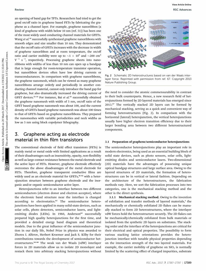
Fig. 3 Schematic illustration (a and c) and optical images (b and d) ofthe vertically stacked graphene/MoS2 heterostructured transistors. (e)The MoS2 layer number dependence of the Ion (current density at VB ¼+0.5 V and VG ¼ +50 V) and Ioff (current density at VB ¼ +0.5 V and VG
¼ �50 V). Reprinted with permission from ref. 71 and 73. Copyright2014 AIP Publishing LLC and 2013 Nature Publishing Group.
Each layer in graphene consists of a covalently bonded,dangling-bond-free lattice and is weakly bound to neighboringlayers by van der Waals interactions. This makes it feasible toisolate, mix and match highly disparate atomic layers to create
17390 | RSC Adv., 2017, 7, 17387–17397
a wide range of van der Waals heterostructures (vdWHs)without the constraints of lattice matching and processingcompatibility.69 Since the discovery of graphene, it became clearthat when a graphene nanosheet is combined with some inor-ganic semiconductors, the zero-gap shortcomings, that limitthe on/off current ratio of graphene-based transistors, could beconsiderably reduced or even avoided.
Graphene/inorganic semiconductor heterojunctions could beclassied as binary19,70–74 and ternary8,75,76 heterostructuresaccording to the components in the heterostructures (Table 1).Graphene-based binary heterojunctions usually include gra-phene/h-BN,19,77 graphene/MoS2,73 graphene/WS2,70 graphene/BP,72 and so on. For example, Yu et al.73 reported the verticalintegration of graphene/MoS2 heterostructures of layered mate-rials for the fabrication of a new generation of vertical eld-effecttransistors (VFETs) with a room temperature on/off current ratio>103 and a high current density of up to 5000 A cm�2 (Fig. 3a andb). Subsequently, Moriya et al.71 further improved the on/off ratioand current density of the VFETs based on graphene/MoS2 het-erostructures to 105 and 104 A cm�2, respectively (Fig. 3c and e).
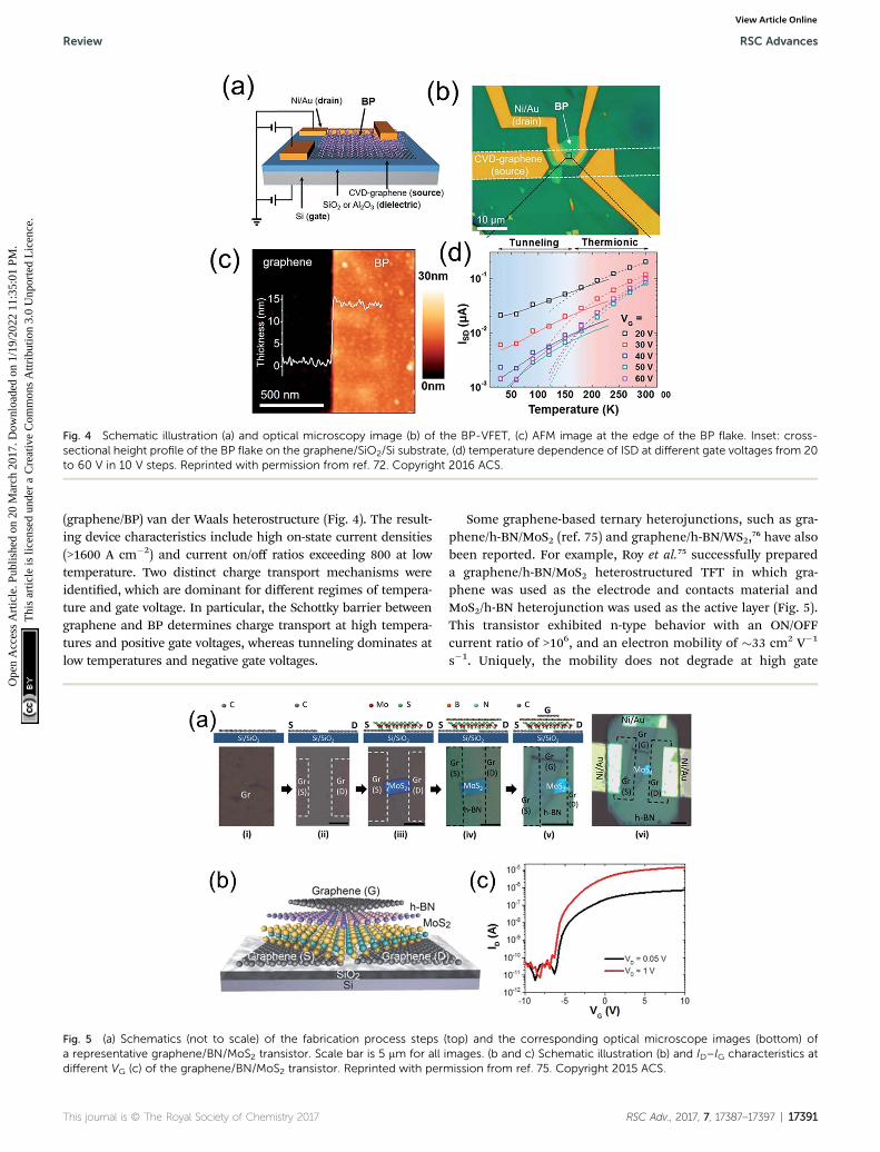
Very recently, Kang et al.72 presented a vertical eld-effecttransistor geometry based on a graphene/black phosphorus
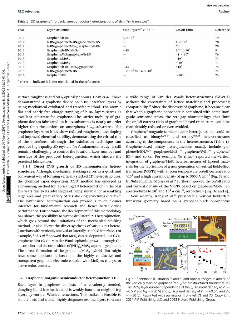
Fig. 4 Schematic illustration (a) and optical microscopy image (b) of the BP-VFET, (c) AFM image at the edge of the BP flake. Inset: cross-sectional height profile of the BP flake on the graphene/SiO2/Si substrate, (d) temperature dependence of ISD at different gate voltages from 20to 60 V in 10 V steps. Reprinted with permission from ref. 72. Copyright 2016 ACS.
Review RSC Advances
Ope
n A
cces
s A
rtic
le. P
ublis
hed
on 2
0 M
arch
201
7. D
ownl
oade
d on
1/1
9/20
22 1
1:35
:01
PM.
Thi
s ar
ticle
is li
cens
ed u
nder
a C
reat
ive
Com
mon
s A
ttrib
utio
n 3.
0 U
npor
ted
Lic
ence
.View Article Online
(graphene/BP) van der Waals heterostructure (Fig. 4). The result-ing device characteristics include high on-state current densities(>1600 A cm�2) and current on/off ratios exceeding 800 at lowtemperature. Two distinct charge transport mechanisms wereidentied, which are dominant for different regimes of tempera-ture and gate voltage. In particular, the Schottky barrier betweengraphene and BP determines charge transport at high tempera-tures and positive gate voltages, whereas tunneling dominates atlow temperatures and negative gate voltages.
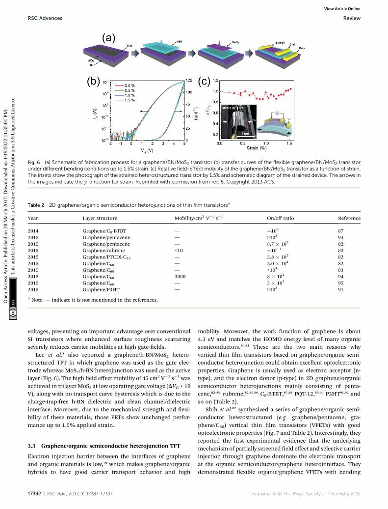
Fig. 5 (a) Schematics (not to scale) of the fabrication process steps (a representative graphene/BN/MoS2 transistor. Scale bar is 5 mm for all idifferent VG (c) of the graphene/BN/MoS2 transistor. Reprinted with perm
Some graphene-based ternary heterojunctions, such as gra-phene/h-BN/MoS2 (ref. 75) and graphene/h-BN/WS2,76 have alsobeen reported. For example, Roy et al.75 successfully prepareda graphene/h-BN/MoS2 heterostructured TFT in which gra-phene was used as the electrode and contacts material andMoS2/h-BN heterojunction was used as the active layer (Fig. 5).This transistor exhibited n-type behavior with an ON/OFFcurrent ratio of >106, and an electron mobility of �33 cm2 V�1
s�1. Uniquely, the mobility does not degrade at high gate
top) and the corresponding optical microscope images (bottom) ofmages. (b and c) Schematic illustration (b) and ID–IG characteristics atission from ref. 75. Copyright 2015 ACS.
Fig. 6 (a) Schematic of fabrication process for a graphene/BN/MoS2 transistor (b) transfer curves of the flexible graphene/BN/MoS2 transistorunder different bending conditions up to 1.5% strain. (c) Relative field-effect mobility of the graphene/BN/MoS2 transistor as a function of strain.The insets show the photograph of the strained heterostructured transistor by 1.5% and schematic diagram of the strained device. The arrows inthe images indicate the y-direction for strain. Reprinted with permission from ref. 8. Copyright 2013 ACS.
Table 2 2D graphene/organic semiconductor heterojunctions of thin film transistorsa
Year Layer structure Mobility/cm2 V�1 s�1 On/off ratio Reference
a Note: — indicate it is not mentioned in the references.
RSC Advances Review
Ope
n A
cces
s A
rtic
le. P
ublis
hed
on 2
0 M
arch
201
7. D
ownl
oade
d on
1/1
9/20
22 1
1:35
:01
PM.
Thi
s ar
ticle
is li
cens
ed u
nder
a C
reat
ive
Com
mon
s A
ttrib
utio
n 3.
0 U
npor
ted
Lic
ence
.View Article Online
voltages, presenting an important advantage over conventionalSi transistors where enhanced surface roughness scatteringseverely reduces carrier mobilities at high gate-elds.
Lee et al.8 also reported a graphene/h-BN/MoS2 hetero-structured TFT in which graphene was used as the gate elec-trode whereas MoS2/h-BN heterojunction was used as the activelayer (Fig. 6). The high eld effect mobility of 45 cm2 V�1 s�1 wasachieved in trilayer MoS2 at low operating gate voltage (DVG < 10V), along with no transport curve hysteresis which is due to thecharge-trap-free h-BN dielectric and clean channel/dielectricinterface. Moreover, due to the mechanical strength and exi-bility of these materials, those FETs show unchanged perfor-mance up to 1.5% applied strain.
Electron injection barrier between the interfaces of grapheneand organic materials is low,79 which makes graphene/organichybrids to have good carrier transport behavior and high
17392 | RSC Adv., 2017, 7, 17387–17397
mobility. Moreover, the work function of graphene is about4.3 eV and matches the HOMO energy level of many organicsemiconductors.80,81 These are the two main reasons whyvertical thin lm transistors based on graphene/organic semi-conductor heterojunction could obtain excellent optoelectronicproperties. Graphene is usually used as electron acceptor (n-type), and the electron donor (p-type) in 2D graphene/organicsemiconductor heterojunctions mainly consisting of penta-cene,82–84 rubrene,82,85,86 C8-BTBT,87,88 PQT-12,89,90 P3HT91,92 andso on (Table 2).
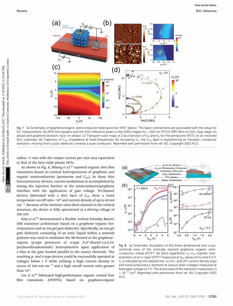
Shih et al.82 synthesized a series of graphene/organic semi-conductor heterostructured (e.g. graphene/pentacene, gra-phene/C60) vertical thin lm transistors (VFETs) with goodoptoelectronic properties (Fig. 7 and Table 2). Interestingly, theyreported the rst experimental evidence that the underlyingmechanism of partially screened eld effect and selective carrierinjection through graphene dominate the electronic transportat the organic semiconductor/graphene heterointerface. Theydemonstrated exible organic/graphene VFETs with bending
Fig. 7 (a) Schematic of graphene/organic semiconductor heterojunction VFET device. The black connections are associated with the setup forDC measurement. (b) AFM micrographs and the (112) reflection peaks in the GIXD images for �100 nm PTCDI-BPE films on SiO2 (top, edge-onphase) and graphene (bottom, face-on phase). (c) Transport color maps of J as a function of VD and VG for the pentacene VFETs on as-receivedSiO2 substrate. (d) Trajectory of C60 impedance at fixed frequencies. By increasing VG, the C60 layer is experiencing an insulator–conductortransition, moving from a pure dielectric towards a pure conductor. Reprinted with permission from ref. 82. Copyright 2015 ACS.
Fig. 8 (a) Schematic illustration of the three-dimensional and cross-sectional view of the vertically stacked graphene–organic semi-conductor–metal VOTFT. (b) Semi-logarithmic ID–VGS transfer char-acteristics of an n-type VOTFTmeasured at Vds values of 0.2 and 0.5 V.IG is indicated by the dashed line. (c) On- and off-current density (top)and transconductance (bottom) at various drain voltages measured atfixed gate voltage of 3 V. The active area of the transistor measured is 3� 10�3 cm2. Reprinted with permission from ref. 83. Copyright 2015ACS.
Review RSC Advances
Ope
n A
cces
s A
rtic
le. P
ublis
hed
on 2
0 M
arch
201
7. D
ownl
oade
d on
1/1
9/20
22 1
1:35
:01
PM.
Thi
s ar
ticle
is li
cens
ed u
nder
a C
reat
ive
Com
mon
s A
ttrib
utio
n 3.
0 U
npor
ted
Lic
ence
.View Article Online
radius <1 mm with the output current per unit area equivalentto that of the best oxide planar FETs.
As shown in Fig. 8, Hlaing et al.83 reported organic thin lmtransistors based on vertical heterojunctions of graphene andorganic semiconductors (pentacene and C60). In these thinheterostructure devices, current modulation is accomplished bytuning the injection barriers at the semiconductor/grapheneinterface with the application of gate voltage. N-Channeldevices fabricated with a thin layer of C60 show a roomtemperature on/off ratio >104 and current density of up to 44mAcm�2. Because of the intrinsic ultra-short channel in the verticalstructure, the device is fully operational at a driving voltage of200 mV.
Kim et al.93 demonstrated a exible vertical Schottky Barrier(SB) transistor architecture based on a graphene–organic het-erojunction and an ion gel gate dielectric. Specically, an ion gelgate dielectric consisting of an ionic liquid within a networkpolymer was used to modulate the SB formed at the graphene–organic (p-type pentacene or n-type N,N0-dioctyl-3,4,9,10-perylenedicarboximide) heterojunction upon application ofa bias at the gate located parallel to the source electrode. Theresulting p- and n-type devices could be successfully operated atvoltages below 1 V while yielding a high current density inexcess of 100 mA cm�2 and a high on/off current ratio greaterthan 103.
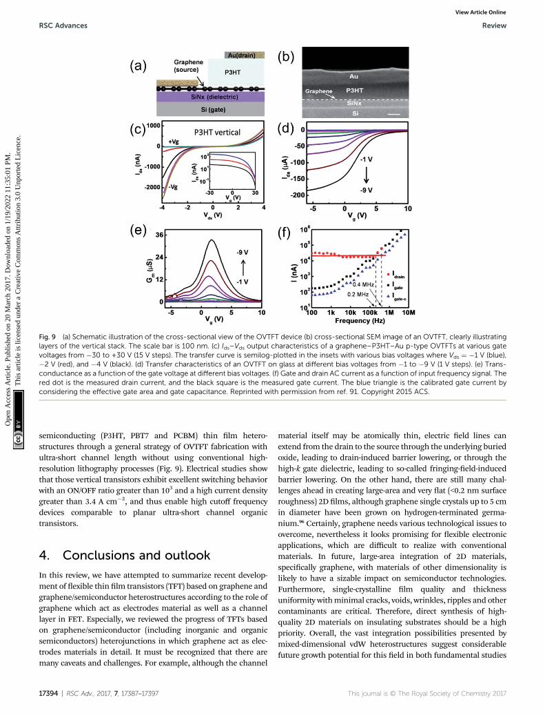
Liu et al.91 fabricated high-performance organic vertical thinlm transistors (OVTFTs) based on graphene/organic
Fig. 9 (a) Schematic illustration of the cross-sectional view of the OVTFT device (b) cross-sectional SEM image of an OVTFT, clearly illustratinglayers of the vertical stack. The scale bar is 100 nm. (c) Ids–Vds output characteristics of a graphene–P3HT–Au p-type OVTFTs at various gatevoltages from �30 to +30 V (15 V steps). The transfer curve is semilog-plotted in the insets with various bias voltages where Vds ¼ �1 V (blue),�2 V (red), and �4 V (black). (d) Transfer characteristics of an OVTFT on glass at different bias voltages from �1 to �9 V (1 V steps). (e) Trans-conductance as a function of the gate voltage at different bias voltages. (f) Gate and drain AC current as a function of input frequency signal. Thered dot is the measured drain current, and the black square is the measured gate current. The blue triangle is the calibrated gate current byconsidering the effective gate area and gate capacitance. Reprinted with permission from ref. 91. Copyright 2015 ACS.
RSC Advances Review
Ope
n A
cces
s A
rtic
le. P
ublis
hed
on 2
0 M
arch
201
7. D
ownl
oade
d on
1/1
9/20
22 1
1:35
:01
PM.
Thi
s ar
ticle
is li
cens
ed u
nder
a C
reat
ive
Com
mon
s A
ttrib
utio
n 3.
0 U
npor
ted
Lic
ence
.View Article Online
semiconducting (P3HT, PBT7 and PCBM) thin lm hetero-structures through a general strategy of OVTFT fabrication withultra-short channel length without using conventional high-resolution lithography processes (Fig. 9). Electrical studies showthat those vertical transistors exhibit excellent switching behaviorwith an ON/OFF ratio greater than 103 and a high current densitygreater than 3.4 A cm�2, and thus enable high cutoff frequencydevices comparable to planar ultra-short channel organictransistors.
4. Conclusions and outlook
In this review, we have attempted to summarize recent develop-ment of exible thin lm transistors (TFT) based on graphene andgraphene/semiconductor heterostructures according to the role ofgraphene which act as electrodes material as well as a channellayer in FET. Especially, we reviewed the progress of TFTs basedon graphene/semiconductor (including inorganic and organicsemiconductors) heterojunctions in which graphene act as elec-trodes materials in detail. It must be recognized that there aremany caveats and challenges. For example, although the channel
17394 | RSC Adv., 2017, 7, 17387–17397
material itself may be atomically thin, electric eld lines canextend from the drain to the source through the underlying buriedoxide, leading to drain-induced barrier lowering, or through thehigh-k gate dielectric, leading to so-called fringing-eld-inducedbarrier lowering. On the other hand, there are still many chal-lenges ahead in creating large-area and very at (<0.2 nm surfaceroughness) 2D lms, although graphene single crystals up to 5 cmin diameter have been grown on hydrogen-terminated germa-nium.96 Certainly, graphene needs various technological issues toovercome, nevertheless it looks promising for exible electronicapplications, which are difficult to realize with conventionalmaterials. In future, large-area integration of 2D materials,specically graphene, with materials of other dimensionality islikely to have a sizable impact on semiconductor technologies.Furthermore, single-crystalline lm quality and thicknessuniformity withminimal cracks, voids, wrinkles, ripples and othercontaminants are critical. Therefore, direct synthesis of high-quality 2D materials on insulating substrates should be a highpriority. Overall, the vast integration possibilities presented bymixed-dimensional vdW heterostructures suggest considerablefuture growth potential for this eld in both fundamental studies
and applied technologies. It is anticipated that further progress in2D material growth, heterostructure formation and device fabri-cation shall lead to practical applications in future.
Acknowledgements
This work was supported by Natural National Science Founda-tion of China and Pakistan Science Foundation Collaborativeresearch project (5161101159), Guangdong Talents Project,NSFC (51373075, 61136003) National Basic Research Programof China (973 Program, No. 2015CB856505; 2015CB93220),Natural Science Foundation of Jiangsu Province (BM2012010),the Shenzhen Peacock Program (KQTD2014062714543296) andShenzhen Key Laboratory of Shenzhen Science and TechnologyPlan (ZDSYS20140509094114164).
References
1 K. S. Novoselov, A. K. Geim, S. V. Morozov, D. Jiang, Y. Zhang,S. V. Dubonos, I. V. Grigorieva and A. A. Firsov, Science, 2004,306(5696), 666–669.
2 G. R. Bhimanapati, Z. Lin, V. Meunier, Y. Jung, J. Cha, S. Das,D. Xiao, Y. Son,M. S. Strano, V. R. Cooper, L. Liang, S. G. Louie,E. Ringe, W. Zhou, S. S. Kim, R. R. Naik, B. G. Sumpter,H. Terrones, F. Xia, Y. Wang, J. Zhu, D. Akinwande, N. Alem,J. A. Schuller, R. E. Schaak, M. Terrones and J. A. Robinson,ACS Nano, 2015, 9(12), 11509–11539.
3 H. Zhang, ACS Nano, 2015, 9(10), 9451–9469.4 C. N. R. Rao, H. S. S. R. Matte and U. Maitra, Angew. Chem.,Int. Ed., 2013, 52(50), 13162–13185.
5 A. Gupta, T. Sakthivel and S. Seal, Prog. Mater. Sci., 2015, 73,44–126.
6 I. Meric, C. R. Dean, N. Petrone, L. Wang, J. Hone, P. Kim andK. L. Shepard, Proc. IEEE, 2013, 101(7), 1609–1619.
7 H. Fang, S. Chuang, T. C. Chang, K. Takei, T. Takahashi andA. Javey, Nano Lett., 2012, 12(7), 3788–3792.
8 G.-H. Lee, Y.-J. Yu, X. Cui, N. Petrone, C.-H. Lee, M. S. Choi,D.-Y. Lee, C. Lee, W. J. Yoo, K. Watanabe, T. Taniguchi,C. Nuckolls, P. Kim and J. Hone, ACS Nano, 2013, 7(9),7931–7936.
9 B. Radisavljevic, A. Radenovic, J. Brivio, V. Giacometti andA. Kis, Nat. Nanotechnol., 2011, 6(3), 147–150.
10 Q. Y. He, Z. Y. Zeng, Z. Y. Yin, H. Li, S. X. Wu, X. Huang andH. Zhang, Small, 2012, 8(19), 2994–2999.
11 J. Pu, Y. Yomogida, K.-K. Liu, L.-J. Li, Y. Iwasa andT. Takenobu, Nano Lett., 2012, 12(8), 4013–4017.
12 A. K. Geim, Science, 2009, 324(5934), 1530–1534.13 D. Jariwala, T. J. Marks and M. C. Hersam, Nat. Mater., 2017,
16(2), 170–181.14 J. C. Meyer, C. Kisielowski, R. Erni, M. D. Rossell,
M. F. Crommie and A. Zettl,Nano Lett., 2008, 8(11), 3582–3586.15 A. K. Geim and K. S. Novoselov, Nat. Mater., 2007, 6(3), 183–
191.16 K. S. Novoselov, V. I. Fal'ko, L. Colombo, P. R. Gellert,
M. G. Schwab and K. Kim, Nature, 2012, 490(7419), 192–200.
17 K. S. Novoselov, A. K. Geim, S. V. Morozov, D. Jiang,M. I. Katsnelson, I. V. Grigorieva, S. V. Dubonos andA. A. Firsov, Nature, 2005, 438(7065), 197–200.
18 K. I. Bolotin, K. J. Sikes, Z. Jiang, M. Klima, G. Fudenberg,J. Hone, P. Kim and H. L. Stormer, Solid State Commun.,2008, 146(9–10), 351–355.
19 C. R. Dean, A. F. Young, I. Meric, C. Lee, L. Wang,S. Sorgenfrei, K. Watanabe, T. Taniguchi, P. Kim,K. L. Shepard and J. Hone, Nat. Nanotechnol., 2010, 5(10),722–726.
20 J.-H. Chen, C. Jang, S. Xiao, M. Ishigami and M. S. Fuhrer,Nat. Nanotechnol., 2008, 3(4), 206–209.
21 S. Hertel, D. Waldmann, J. Jobst, A. Albert, M. Albrecht,S. Reshanov, A. Schoner, M. Krieger and H. B. Weber, Nat.Commun., 2012, 3, 957.
22 M. F. El-Kady, V. Strong, S. Dubin and R. B. Kaner, Science,2012, 335(6074), 1326–1330.
23 R. R. Nair, P. Blake, A. N. Grigorenko, K. S. Novoselov,T. J. Booth, T. Stauber, N. M. R. Peres and A. K. Geim,Science, 2008, 320(5881), 1308.
24 J. Lu, J.-x. Yang, J. Wang, A. Lim, S. Wang and K. P. Loh, ACSNano, 2009, 3(8), 2367–2375.
25 G. Eda and M. Chhowalla, Adv. Mater., 2010, 22(22), 2392–2415.
26 H. Liu, T. Ye and C. Mao, Angew. Chem., Int. Ed., 2007, 46(34),6473–6475.
28 Y.-R. Chang, H.-Y. Lee, K. Chen, C.-C. Chang, D.-S. Tsai,C.-C. Fu, T.-S. Lim, Y.-K. Tzeng, C.-Y. Fang, C.-C. Han,H.-C. Chang and W. Fann, Nat. Nanotechnol., 2008, 3(5),284–288.
29 C. Lee, X. Wei, J. W. Kysar and J. Hone, Science, 2008,321(5887), 385–388.
30 A. A. Balandin, S. Ghosh, W. Bao, I. Calizo, D. Teweldebrhan,F. Miao and C. N. Lau, Nano Lett., 2008, 8(3), 902–907.
31 K. S. Novoselov, Z. Jiang, Y. Zhang, S. V. Morozov,H. L. Stormer, U. Zeitler, J. C. Maan, G. S. Boebinger,P. Kim and A. K. Geim, Science, 2007, 315(5817), 1379.
32 M. I. Katsnelson, K. S. Novoselov and A. K. Geim, Nat. Phys.,2006, 2(9), 620–625.
33 P. K. Weimer, Proc. IRE, 1962, 50(6), 1462–1469.34 A. Dodabalapur, Mater. Today, 2006, 9(4), 24–30.35 T. Someya, Y. Kato, T. Sekitani, S. Iba, Y. Noguchi, Y. Murase,
H. Kawaguchi and T. Sakurai, Proc. Natl. Acad. Sci. U. S. A.,2005, 102(35), 12321–12325.
36 J. A. Rogers, Z. Bao, K. Baldwin, A. Dodabalapur, B. Crone,V. R. Raju, V. Kuck, H. Katz, K. Amundson, J. Ewing andP. Drzaic, Proc. Natl. Acad. Sci. U. S. A., 2001, 98(9), 4835–4840.
37 A. Schlierf, P. Samori and V. Palermo, J. Mater. Chem. C,2014, 2(17), 3129–3143.
38 B. K. Sharma and J. H. Ahn, Solid-State Electron., 2013, 89,177–188.
39 D. Akinwande, N. Petrone and J. Hone, Nat. Commun., 2014,5, 5678.
40 G. Fiori, F. Bonaccorso, G. Iannaccone, T. Palacios,D. Neumaier, A. Seabaugh, S. K. Banerjee and L. Colombo,Nat. Nanotechnol., 2014, 9(10), 768–779.
41 S. J. Park, O. S. Kwon, S. H. Lee, H. S. Song, T. H. Park andJ. Jang, Nano Lett., 2012, 12(10), 5082–5090.
42 C. Sire, F. Ardiaca, S. Lepilliet, J. W. T. Seo, M. C. Hersam,G. Darnbrine, H. Happy and V. Derycke, Nano Lett., 2012,12(3), 1184–1188.
43 C. Biswas and Y. H. Lee, Adv. Funct. Mater., 2011, 21(20),3806–3826.
44 Q. Y. He, S. X. Wu, Z. Y. Yin and H. Zhang, Chem. Sci., 2012,3(6), 1764–1772.
45 B. B. Zhan, C. Li, J. Yang, G. Jenkins, W. Huang andX. C. Dong, Small, 2014, 10(20), 4042–4065.
46 S. Lee, K. Lee, C.-H. Liu, G. S. Kulkarni and Z. Zhong, Nat.Commun., 2012, 3, 1018.
47 Q. H. Wang, K. Kalantar-Zadeh, A. Kis, J. N. Coleman andM. S. Strano, Nat. Nanotechnol., 2012, 7(11), 699–712.
48 J. Lee, T.-J. Ha, H. Li, K. N. Parrish, M. Holt, A. Dodabalapur,R. S. Ruoff and D. Akinwande, ACS Nano, 2013, 7(9), 7744–7750.
49 R. C. Cooper, C. Lee, C. A. Marianetti, X. Wei, J. Hone andJ. W. Kysar, Phys. Rev. B: Condens. Matter Mater. Phys.,2013, 87(3), 035423.
50 Z. Johari and R. Ismail, Sci. Adv. Mater., 2015, 7(10), 2011–2020.
51 X. Li, X. Wang, L. Zhang, S. Lee and H. Dai, Science, 2008,319(5867), 1229–1232.
52 X. Wang, Y. Ouyang, X. Li, H. Wang, J. Guo and H. Dai, Phys.Rev. Lett., 2008, 100(20), 1586–1594.
53 S. Berrada, N. Viet Hung, D. Querlioz, J. St-Martin,A. Alarcon, C. Chassat, A. Bournel and P. Dollfus, Appl.Phys. Lett., 2013, 103(18), 183509.
54 I. Jung, H. Y. Jang, J. Moon and S. Park, Nanoscale, 2014,6(12), 6482–6486.
55 J. Bai, X. Zhong, S. Jiang, Y. Huang and X. Duan, Nat.Nanotechnol., 2010, 5(3), 190–194.
56 Y. Song, W. Fang, R. Brenes and J. Kong, Nano Today, 2015,10(6), 681–700.
57 C.-a. Di, D. Wei, G. Yu, Y. Liu, Y. Guo and D. Zhu, Adv. Mater.,2008, 20(17), 3289–3293.
58 G. Wang, Y. Kim, M. Choe, T.-W. Kim and T. Lee, Adv. Mater.,2011, 23(6), 755–760.
59 H. Chang, G. Wang, A. Yang, X. Tao, X. Liu, Y. Shen andZ. Zheng, Adv. Funct. Mater., 2010, 20(17), 2893–2902.
60 W. Liu, B. L. Jackson, J. Zhu, C.-Q. Miao, C.-H. Chung,Y.-J. Park, K. Sun, J. Woo and Y.-H. Xie, ACS Nano, 2011,5(3), 2412.
61 J. Y. Choi, W. Kang, B. Kang, W. Cha, S. K. Son, Y. Yoon,H. Kim, Y. Kang, M. J. Ko, H. J. Son, K. Cho, J. H. Cho andB. Kim, ACS Appl. Mater. Interfaces, 2015, 7(10), 6002–6012.
62 W. H. Lee, J. Park, S. H. Sim, S. B. Jo, K. S. Kim, B. H. Hongand K. Cho, Adv. Mater., 2011, 23(15), 1752–1756.
63 R. L. Anderson, Solid-State Electron., 1962, 5(SEP-O), 341–344.
17396 | RSC Adv., 2017, 7, 17387–17397
64 Z. I. Alferov, V. M. Andreev, D. Z. Garbuzov, Y. V. Zhilyaev,E. P. Morozov, E. L. Portnoi and V. G. Trom, Fiz. Tekh.Poluprovodn., 1970, 4(9), 1826–1829.
65 I. Hayashi, M. B. Panish and P. W. Foy, IEEE J. QuantumElectron., 1969, 5(4), 211–212.
66 H. Kressel and H. Nelson, RCA Rev., 1969, 30(1), 106–113.67 A. K. Geim and I. V. Grigorieva, Nature, 2013, 499(7459), 419–
425.68 Y. Shi, W. Zhou, A.-Y. Lu, W. Fang, Y.-H. Lee, A. L. Hsu,
S. M. Kim, K. K. Kim, H. Y. Yang, L.-J. Li, J.-C. Idrobo andJ. Kong, Nano Lett., 2012, 12(6), 2784–2791.
69 Y. Liu, N. O. Weiss, X. Duan, H.-C. Cheng, Y. Huang andX. Duan, Nat. Rev. Mater., 2016, 16042.
70 H. Tan, Y. Fan, Y. Rong, B. Porter, C. S. Lau, Y. Zhou, Z. He,S. Wang, H. Bhaskaran and J. H. Warner, ACS Appl. Mater.Interfaces, 2016, 8(3), 1644–1652.
71 R. Moriya, T. Yamaguchi, Y. Inoue, S. Morikawa, Y. Sata,S. Masubuchi and T. Machida, Appl. Phys. Lett., 2014,105(8), 083119.
72 J. Kang, D. Jariwala, C. R. Ryder, S. A. Wells, Y. Choi,E. Hwang, J. H. Cho, T. J. Marks and M. C. Hersam, NanoLett., 2016, 16(4), 2580–2585.
73 W. J. Yu, Z. Li, H. Zhou, Y. Chen, Y. Wang, Y. Huang andX. Duan, Nat. Mater., 2013, 12(3), 246–252.
74 M. A. Stolyarov, G. Liu, S. L. Rumyantsev, M. Shur andA. A. Balandin, Appl. Phys. Lett., 2015, 107(2), 023106.
75 T. Roy, M. Tosun, J. S. Kang, A. B. Sachid, S. B. Desai,M. Hettick, C. C. Hu and A. Javey, ACS Nano, 2014, 8(6),6259–6264.
76 T. Georgiou, R. Jalil, B. D. Belle, L. Britnell, R. V. Gorbachev,S. V. Morozov, Y.-J. Kim, A. Gholinia, S. J. Haigh,O. Makarovsky, L. Eaves, L. A. Ponomarenko, A. K. Geim,K. S. Novoselov and A. Mishchenko, Nat. Nanotechnol.,2013, 8(2), 100–103.
77 S. J. Kang, G.-H. Lee, Y.-J. Yu, Y. Zhao, B. Kim, K. Watanabe,T. Taniguchi, J. Hone, P. Kim and C. Nuckolls, Adv. Funct.Mater., 2014, 24(32), 5157–5163.
78 L. Britnell, R. V. Gorbachev, R. Jalil, B. D. Belle, F. Schedin,A. Mishchenko, T. Georgiou, M. I. Katsnelson, L. Eaves,S. V. Morozov, N. M. R. Peres, J. Leist, A. K. Geim,K. S. Novoselov and L. A. Ponomarenko, Science, 2012,335(6071), 947–950.
79 S. Lee, G. Jo, S.-J. Kang, G. Wang, M. Choe, W. Park,D.-Y. Kim, Y. H. Kahng and T. Lee, Adv. Mater., 2011, 23(1),100–105.
80 Y. Shi, K. K. Kim, A. Reina, M. Hofmann, L.-J. Li and J. Kong,ACS Nano, 2010, 4(5), 2689–2694.
81 Y.-J. Yu, Y. Zhao, S. Ryu, L. E. Brus, K. S. Kim and P. Kim,Nano Lett., 2009, 9(10), 3430–3434.
82 C.-J. Shih, R. Pfattner, Y.-C. Chiu, N. Liu, T. Lei, D. Kong,Y. Kim, H.-H. Chou, W.-G. Bae and Z. Bao, Nano Lett.,2015, 15(11), 7587–7595.
83 H. Hlaing, C.-H. Kim, F. Carta, C.-Y. Nam, R. A. Barton,N. Petrone, J. Hone and I. Kymissis, Nano Lett., 2015, 15(1),69–74.
84 D. Jariwala, S. L. Howell, K.-S. Chen, J. Kang, V. K. Sangwan,S. A. Filippone, R. Turrisi, T. J. Marks, L. J. Lauhon andM. C. Hersam, Nano Lett., 2016, 16(1), 497–503.
85 C.-H. Lee, T. Schiros, E. J. G. Santos, B. Kim, K. G. Yager,S. J. Kang, S. Lee, J. Yu, K. Watanabe, T. Taniguchi,J. Hone, E. Kaxiras, C. Nuckolls and P. Kim, Adv. Mater.,2014, 26(18), 2812–2817.
86 F. Liu, W. L. Chow, X. He, P. Hu, S. Zheng, X. Wang, J. Zhou,Q. Fu, W. Fu, P. Yu, Q. Zeng, H. J. Fan, B. K. Tay, C. Kloc andZ. Liu, Adv. Funct. Mater., 2015, 25(36), 5865–5871.
87 D. He, Y. Zhang, Q. Wu, R. Xu, H. Nan, J. Liu, J. Yao, Z. Wang,S. Yuan, Y. Li, Y. Shi, J. Wang, Z. Ni, L. He, F. Miao, F. Song,H. Xu, K. Watanabe, T. Taniguchi, J.-B. Xu and X. Wang, Nat.Commun., 2014, 5, 5162.
88 D. He, Y. Pan, H. Nan, S. Gu, Z. Yang, B. Wu, X. Luo, B. Xu,Y. Zhang, Y. Li, Z. Ni, B. Wang, J. Zhu, Y. Chai, Y. Shi andX. Wang, Appl. Phys. Lett., 2015, 107(18), 183103.
89 J. Huang, D. R. Hines, B. J. Jung, M. S. Bronsgeest,A. Tunnell, V. Ballarotto, H. E. Katz, M. S. Fuhrer,
93 B. J. Kim, E. Hwang, M. S. Kang and J. H. Cho, Adv. Mater.,2015, 27(39), 5875–5881.
94 S. Parui, L. Pietrobon, D. Ciudad, S. Velez, X. Sun,F. Casanova, P. Stoliar and L. E. Hueso, Adv. Funct. Mater.,2015, 25(20), 2972–2979.
95 K. Kim, T. H. Lee, E. J. G. Santos, P. S. Jo, A. Salleo, Y. Nishiand Z. Bao, ACS Nano, 2015, 9(6), 5922–5928.
96 B. Wu, Y. Zhao, H. Nan, Z. Yang, Y. Zhang, H. Zhao, D. He,Z. Jiang, X. Liu, Y. Li, Y. Shi, Z. Ni, J. Wang, J.-B. Xu andX. Wang, Nano Lett., 2016, 16(6), 3754–3759.