Thin, Flexible Sensors and Actuators as ‘Instrumented’ Surgical Sutures for Targeted Wound Monitoring and Therapy
Dae-Hyeong Kim , Shuodao Wang , Hohyun Keum , Roozbeh Ghaffari , Yun-Soung Kim , Hu Tao , Bruce Panilaitis , Ming Li , Zhan Kang , Fiorenzo Omenetto , Yonggang Huang , and John A. Rogers *
Sutures are among the simplest and most widely used devices
in clinical medicine. All existing synthetic and natural forms
use thread-like geometries, as purely passive, mechanical
structures that are fl exible and resilient to tensile stress.
Several recent reports describe strategies to incorporate
advanced functionality into this platform through the employ-
ment of shape-memory polymers that offer mechanical actua-
tion or through the release of bioresorbable compounds that
carry growth factors and antibiotics to accelerate healing. [ 1–3 ]
Such technologies lack, however, programmable actuation or
sensory feedback control. Sutures that embed fl exible sensors
Prof. D.-H. Kim School of Chemical and Biological Engineering WCU Program of Chemical Convergence for Energy and Environment Institute of Chemical Processes Inter-University Semiconductor Research Center Seoul National University Seoul 151-741, Republic of Korea
Dr. S. Wang, H. Keum, Y.-S. Kim, Prof. J. A. Rogers Department of Materials Science and Engineering Beckman Institute for Advanced Science and Technology and Frederick Seitz Materials Research Laboratory University of Illinois at Urbana-Champaign Urbana, IL 61801, USA E-mail: [email protected]
Dr. R. Ghaffari MC10 Inc., 36 Cameron Avenue Cambridge, MA 02140, USA
Dr. H. Tao, Dr. B. Panilaitis, Prof. F. Omenetto Department of Biomedical Engineering Tufts University, Medford, MA 02155, USA
M. Li, Prof. Z. Kang State Key Laboratory of Structural Analysis for Industrial Equipment Dalian University of Technology Dalian 116024, China
Prof. Y. Huang Department of Mechanical Engineering and Department of Civil and Environmental Engineering Northwestern University Evanston, IL 60208, USA
small 2012, 8, No. 21, 3263–3268
and associated electronic circuits could perform these and
other related functions. Demonstrations using thin fl exible
strips equipped with sensors for pressure and chemical moni-
toring have been reported [ 4 , 5 ] but not in designs for use as
sutures. Furthermore, the organic and silver-based material
components comprising these devices might limit their per-
formance capabilities, and also lead to concerns about long-
term durability in moist, dynamic conditions in the body.
Here, we report strips with signifi cantly smaller form factors,
specifi cally engineered for use as fl exible sutures ( ∼ 1 mm
width and ∼ 3 μ m thickness) ‘instrumented’ with high quality
single crystal inorganic semiconductors of biocompatible
materials such as silicon in nanomembrane formats. [ 6 ] The
resulting class of technology offers routes to high levels of
performance and sophisticated function in sensors and actua-
tors suitable for in vivo use. This new type of diagnostic/ther-
apeutic tools could monitor, sense and actuate in a manner
coordinated with natural biological responses in the body for
improved health outcomes.
The systems described in the following use ultrathin,
narrow strips of biocompatible polymers as platforms for
integrated single crystal silicon nanomembranes (Si NM)
electronics and sensors, confi gured together in ways that
provide requisite mechanical properties. The examples
focus on measurement and delivery of heat, using systems
composed of Si NMs, multicomponent metallization and
dielectric interlayers/encapsulants, all in bifacial designs
(i.e. devices and interconnects on both sides of a thin sub-
strate). The collective properties, including operational com-
patibility with complete immersion in water and biofl uids [ 7 ]
and robustness to large stresses/strains that occur during
suturing, are demonstrated through in vivo evaluations using
animal models. The envisioned clinical context is for sensing
and programmable delivery of local heating and electrical
stimulation to promote healing of chronic wounds [ 8 , 9 ] or for
heat shock strategies in cancer treatment. [ 10 ] Additional pos-
sibilities exist in thermally activated drug release from tem-
perature sensitive, polymer host matrices as coatings onto
these devices. [ 11 ]
A representative system includes Si NM diode tem-
perature sensors and microscale Joule heating elements
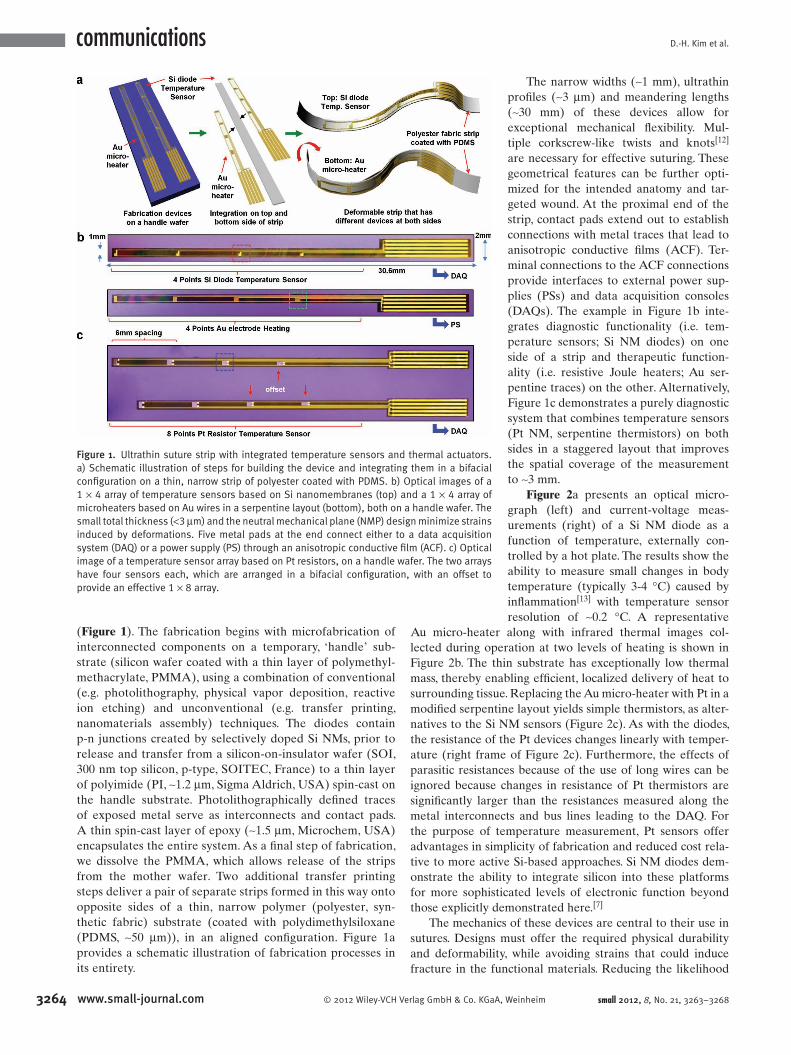
Figure 1 . Ultrathin suture strip with integrated temperature sensors and thermal actuators. a) Schematic illustration of steps for building the device and integrating them in a bifacial confi guration on a thin, narrow strip of polyester coated with PDMS. b) Optical images of a 1 × 4 array of temperature sensors based on Si nanomembranes (top) and a 1 × 4 array of microheaters based on Au wires in a serpentine layout (bottom), both on a handle wafer. The small total thickness ( < 3 μ m) and the neutral mechanical plane (NMP) design minimize strains induced by deformations. Five metal pads at the end connect either to a data acquisition system (DAQ) or a power supply (PS) through an anisotropic conductive fi lm (ACF). c) Optical image of a temperature sensor array based on Pt resistors, on a handle wafer. The two arrays have four sensors each, which are arranged in a bifacial confi guration, with an offset to provide an effective 1 × 8 array.
( Figure 1 ). The fabrication begins with microfabrication of
interconnected components on a temporary, ‘handle’ sub-
strate (silicon wafer coated with a thin layer of polymethyl-
methacrylate, PMMA), using a combination of conventional
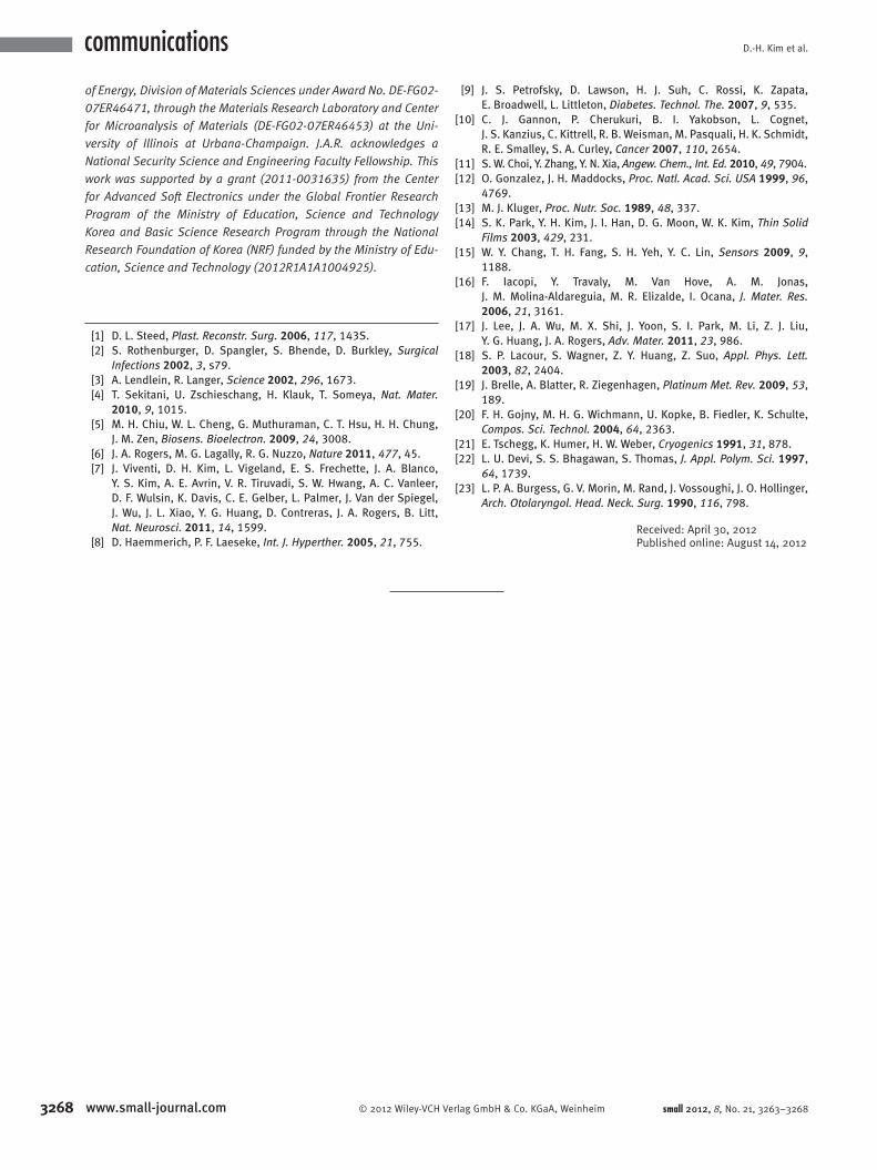
Au micro-heater along with infrared thermal images col-
lected during operation at two levels of heating is shown in
Figure 2 b. The thin substrate has exceptionally low thermal
mass, thereby enabling effi cient, localized delivery of heat to
surrounding tissue. Replacing the Au micro-heater with Pt in a
modifi ed serpentine layout yields simple thermistors, as alter-
natives to the Si NM sensors (Figure 2 c). As with the diodes,
the resistance of the Pt devices changes linearly with temper-
ature (right frame of Figure 2 c). Furthermore, the effects of
parasitic resistances because of the use of long wires can be
ignored because changes in resistance of Pt thermistors are
signifi cantly larger than the resistances measured along the
metal interconnects and bus lines leading to the DAQ. For
the purpose of temperature measurement, Pt sensors offer
advantages in simplicity of fabrication and reduced cost rela-
tive to more active Si-based approaches. Si NM diodes dem-
onstrate the ability to integrate silicon into these platforms
for more sophisticated levels of electronic function beyond
those explicitly demonstrated here. [ 7 ]
The mechanics of these devices are central to their use in
sutures. Designs must offer the required physical durability
and deformability, while avoiding strains that could induce
fracture in the functional materials. Reducing the likelihood
Weinheim small 2012, 8, No. 21, 3263–3268
Thin, Flexible Sensors and Actuators as Surgical Sutures
Figure 2 . Images and characterization data from individual devices, with designs optimized for integration onto thin, narrow suture strips. a) Microscope image of a Si NM diode-based temperature sensor (left) and its characterization results (right). Voltage readings at constant current from current-voltage curves at different temperatures (right frame) show a linear behavior (inset). b, Microscope image of an Au microheater (left) and infrared camera images of heating produced at different currents (right). c, Microscope image of a Pt resistor-based temperature sensor (left) and its calibration results at different temperatures (right). The slope of the resistance versus temperature is ∼ 2.7 Ω / ° C.
of fracture can be challenging, particularly when the devices
incorporate brittle materials such as silicon (fracture strain ∼
1%). To avoid mechanical failure, thin, narrow geometries are
benefi cial because they can accommodate strains induced by
bending. For example, plastic substrates used in typical fl ex-
ible electronic devices (thicknesses ∼ 100 μ m) with standard,
surface-mounted designs have bending stiffness character-
istics that are two orders of magnitude greater than those
associated with the sutures reported here. In addition, the top
layer of epoxy positions the active materials within or near
the neutral mechanical plane (NMP), thus further reducing
strains in the most brittle elements (e.g. silicon).
The essential mechanical properties can all be captured
quantitatively by simple calculations and modeling. A cross-
section of a representative device appears in Figure 3 a (left
frame). The Young’s moduli, thicknesses and widths of the
different layers are denoted as E i , h i and w , respectively.
The device elements (the golden or dark grey bricks shown
in Figure 3 a) are much thinner (50 ∼ 150 nm) and narrower
(40 μ m) than the PI ( h PI = 1.2 μ m, w = 1.0 mm) bottom and
epoxy ( h epoxy = 1.5 μ m, w = 1.0 mm) top layers; their infl uence on
the bending characteristics are negligible ( < 0.2% error). The
bending stiffness of the suture in the width direction is given
by
(E I) =N∑
i= 1
Ei hiw
⎡⎣
⎛⎝y0 −
i∑j = 1
h j
⎞⎠
2
+
⎛⎝y0 −
i∑j = 1
h j
⎞⎠ hi +
1
3h2
i
⎤⎦,
(1)
where N = 3 is the number of layers and y 0 is the position of
NMP (Figure 3 a)
y0 =N∑
i=1
Ei hi
⎛⎝ i∑
j=1
h j − 1
2hi
⎞⎠
/N∑
i=1
Ei hi ,
(2)
and E 1 = E PI = 2.5 GPa [ 14 , 15 ] E 2 = E SiO2 = 73 GPa, [ 16 ] E 3 =
E epoxy = 4.4 GPa, [ 17 ] h 1 = h PI , h 2 = h SiO2 = 50 nm, h 3 = h epoxy .
The bending stiffness calculated from Equations (1-2) is
5.9 × 10 − 12 N · m 2 , which is consistent with values (6.2 × 10 − 12
N · m 2 ) obtained with fi nite element analysis (FEA). For many
applications, the suture mainly undergoes various forms of
bending (Figure 3 b, c). The bending strain in the suture is
expressed as
ε = |y|
R,
(3)
where y is the distance from the NMP (Figure 3 a) and R is
the bending radius. NMP is given by Equation (2) as y 0 =
1.47 μ m, which is just 0.02 μ m above the Au layer. As a result,
the strain remains small even when the suture is in a bending
state (e.g. | ε | = 0.5% in Pt when R = 0.44 mm).
A representative example of a smart suture strip con-
taining temperature sensors and Au electrodes is shown in
Figure 3 b. The ultrathin design, the NMP confi guration and
the use of PDMS as a strain isolation layer on a polyester
strip (Figure 3 a, right frame) enable large deformations, such
as those involved during suturing (second and third frame of
Figure 3 b) as well as knotting (last frame of Figure 3 b). Since
the PDMS layers are much softer and thicker ( ∼ 250 kPa,
50 μ m) than the device strips ( > 2 GPa, 2.7 μ m), the PDMS
(Figure 3 a, right frame) absorbs most of the strain deforma-
tions that result from bending. The PDMS layer provides
this strain isolation without signifi cantly shifting the loca-
tion of the NMP. For suturing (Figure 3 b, middle frames),
the bending radius at the most severely deformed region is
estimated to be R ∼ 2 mm, giving rise to a maximum bending
strain in the gold layer of 0.0085% ( Equation 3 ), consistent
with 0.0081% given by FEA (Figure 3 d).
These fabrication sequences and device designs can
accommodate a wide range of substrate materials. To achieve
minimal thickness in a fi nal, deployed state, bioresorbable
materials, such as silk, can be used (middle frame of Figure 3 c).
The location of the NMP for a suture strip with Pt tem-
perature sensors is schematically shown in the left frame of
Figure 3 c. Because of enhanced fl exibility after dissolving the
underlying silk substrate, folding around a thin glass slide
(middle frame of Figure 3 c) and wrapping around a fi ngertip
(right frame of Figure 3 c) are both possible. In the case of
folding the suture around a sharp glass edge (thickness
1.3 mm) the bending radius of the suture at the sharp edge is
estimated to be R ∼ 1.3 mm and the corresponding maximum
strain given by Eq. (3) is 0.012% for the gold, consistent
with 0.013% given by FEA (Figure 3 e). The zigzag shape of
3265www.small-journal.combH & Co. KGaA, Weinheim
D.-H. Kim et al.
3266
communications
Figure 3 . Mechanics of thin, instrumented suture strips. a) Schematic illustrations of the cross section of a bifacial suture. b) Optical image of a suture strip in its curled form (fi rst frame) and after suturing (second and third frame) and knotting (last frame). c) Optimized mechanical structure shown in a schematic illustration (left frame) and examples of a device under various deformations, such as folding (center frame) and wrapping (right frame). d) Strain distribution for the deformation of Figure 3 b (middle frame). e) Strain distribution for the deformation of Figure 3 c (middle frame).
the Pt sensor (Figure 2 c) further reduces the strain in this
material to only 0.0098% (obtained by FEA). In addition
to minimizing the thickness of the residual, active devices,
bioresorbable substrates can facilitate intimate coupling to
biological tissue surfaces with complex surface texture, such
as the brain ( Figure 4 a).
In vivo animal experiments provide evidence for the prac-
tical use of this new class of devices. Specifi cally, sutures that
use silk substrates were evaluated in anaesthetized mouse
models. After anesthesia delivery, the dorsal side was wiped
with alcohol at the incision site with 70% ethanol and the
incision was sutured with a customized 16-gauge needle and
the smart suture to seal the wound.
Incisions made through the dorsal epidermal layer
allowed partial implantation of the Pt temperature sensor
strip, as shown in the left frame of Figure 4 b. No leakage cur-
rents were observed and temperature measurements showed
stable values around ∼ 26.5 ° C. The right frame of Figure 4 b
shows an image of sensors after removal of the partially
implanted strip from the animal body. The implanted part
shows entanglement that results from the high fl exibility that
follows dissolution of the silk. Some amount of un-implanted
silk, however, remains and maintains the original shape of
the strip, which facilitates handling. The same experiment is
performed with Pt temperature sensors (Figure 4 c). The left
egies developed in this study enable a new class of sutures
with electronic ‘instrumentation’ for advanced functionality
in monitoring the state of wound sites and, potentially, pro-
viding therapeutic operation. Sensing and therapy functions
in sutures can exploit device-quality Si based elements, giving
rise to a wide range of clinical applications, including delivery
of light, chemical and electrical stimuli locally to wound sites.
Experimental Section
Fabrication of Silicon NM Temperature Sensors : The fab-rication began with spin coating a thin polyimide fi lm (PI, ∼ 1.2 μ m, Sigma Aldrich, USA) on top of a sacrifi cial layer of poly(methylmethacrylate) (PMMA, 100 nm, MicroChem, USA) on a handle wafer. Doped single crystalline Si NMs (300 nm) were then transfer printed from a source wafer (n-type SOI wafer, SOITEC, France) to the PI fi lm. The transferred Si NMs were etched to defi ne active regions of pn diodes by using patterns defi ned by photoli-thography and reactive ion etching (RIE). Evaporating metal fi lms (Cr/Au, 5 nm/150 nm) followed by photolithography and wet etching formed metal interconnections between the pn diodes and an external DAQ system. A top insulation layer was formed by spin coating of a thin overcoat of epoxy ( ∼ 1.5 μ m). Oxygen reactive ion etching (RIE) defi ned the overall dimensions of the strip, as shown
, Weinheim small 2012, 8, No. 21, 3263–3268
Thin, Flexible Sensors and Actuators as Surgical Sutures
Figure 4 . Applications of thin, instrumented suture strips. a) Representative device on a plastic model of the human brain before (left frame) and after (right frame) dissolving a temporary silk substrate. b) Temperature monitoring experiment on an animal model using an instrumented suture strip based on a Pt thermistor on silk substrate. No leakage current is measured before (left frame) and after (center frame) dissolving the silk substrate. c) Temperature monitoring using an instrumented suture strip at the location of an incision on an animal model. Schematic illustration of a suture strip and needle (left frame) and corresponding image after suturing (right frame). Temperature differences inside and outside of the epidermis can be monitored by suturing the incision.
in the top frame of Figure 1 b. Transfer printing to a polyester sub-strate coated with PDMS or a silk substrate, and connecting an ACF cable for external wiring to a DAQ completed the process. For enhanced adhesion, a thin bilayer of Ti/SiO 2 (3 nm/30 nm) can be deposited onto the polyester or silk.
Fabrication of Pt Temperature Sensors : The overall shapes and fabrication procedures were similar to those used for the silicon devices. For temperature sensing, however, Pt resistors, instead of Si NM p-n diodes, were located in the island region. Thin layers of Ti/Pt (5 nm/50 nm) deposited with an electron beam (e-beam) evaporator on patterns of photoresist, followed by lift-off formed the Pt resistors. Deposition of Cr/Au (5/150 nm) established interconnection bus lines to each temperature sensor. Surface treatment of the PI with UV/Ozone or deposition of a thin silicon dioxide (SiO 2 ) layer ( ∼ 50 nm) on top of the PI improved the adhe-sion of the Pt. Additional encapsulation with thin fi lms of epoxy formed insulation layers to prevent electrical leakage currents. The fi nal device is shown in Figure 1 c. The steps for transfer printing and connecting to ACF were the same as those for the silicon NM devices.
Fabrication of Au Heaters : The overall shapes and fabrication procedures were sim-ilar to those for the Pt devices. After deposi-tion of Cr/Au (5/150 nm) by electron beam evaporation, wet chemical etching defi ned patterns of Au for resistive heaters. Final pas-sivation with fi lms of epoxy and etching to defi ne the strip geometries completed the fabrication. The resulting device is shown in the bottom frame of Figure 1 b. The steps for transfer printing and connecting to ACF were the same as those for the silicon NM devices.
Silk Preparation : The purifi cation of silk fi broin from Bombyx mori cocoons initially involved removal of sericin, a water-soluble glycoprotein that binds fi broin fi laments, by boiling the cocoons in a 0.02 M aqueous solution of sodium carbonate for 30 min. The resulting fi broin bundle was dried and then dis-solved in a 9.3 M aqueous solution of lithium bromide at 60 ° C for 4 h. The lithium bromide salt was then extracted through a water-based dialysis process over several days. The resulting solution was centrifuged and fi ltered via syringe based micro-fi ltration (5 μ m pore size, Millipore Inc., Bedford, MA) to remove any remaining particulates. This process enables the produc-tion of ∼ 6.5% w/v silk fi broin solution with minimal contaminants and reduced scattering for optical applications. After production of the silk fi broin solution, 10 mL of the solution was cast on 4-inch Si wafers and allowed to crystal-lize in air ( ∼ 12 h). The resulting fi lms were then removed from the substrate and were approxi-mately 50 μ m thick.
Animal Experiments : All procedures were carried out under approved animal protocols. A female Balb/c mouse was anaesthetized with an intraperitoneal injection of a mix of
ketamine–xylazine. The depth of anaesthesia was monitored by palpebral and withdrawal refl exes to confi rm that the animal had reached ‘stage 3’ of anaesthesia. Once the animal was lightly anaesthetized, the dorsal area was shaved and scrubbed with alcohol (70% ethanol) at the incision site, followed with a beta-dine surgical scrub. To validate the performance of sutures in real conditions, the incision opened during surgery was closed with a customized 16-gauge needle and three passes with the tempera-ture sensing suture were carried out to seal the wound. We then verifi ed the operation of the temperature sensors in the animal. In all instances, the incisions were carried out on the dorsal side of the mouse and the suturing was carried out across the dermal layers above the musculature.
Acknowledgements
This material is based upon work supported by the National Science Foundation under grant #0749028 (CMMI) and the US Department
3267www.small-journal.comm
D.-H. Kim et al.
32
communications
[ 1 ] D. L. Steed , Plast. Reconstr. Surg. 2006 , 117 , 143S . [ 2 ] S. Rothenburger , D. Spangler , S. Bhende , D. Burkley , Surgical
Infections 2002 , 3 , s79 . [ 3 ] A. Lendlein , R. Langer , Science 2002 , 296 , 1673 . [ 4 ] T. Sekitani , U. Zschieschang , H. Klauk , T. Someya , Nat. Mater.
2010 , 9 , 1015 . [ 5 ] M. H. Chiu , W. L. Cheng , G. Muthuraman , C. T. Hsu , H. H. Chung ,
J. M. Zen , Biosens. Bioelectron. 2009 , 24 , 3008 . [ 6 ] J. A. Rogers , M. G. Lagally , R. G. Nuzzo , Nature 2011 , 477 , 45 . [ 7 ] J. Viventi , D. H. Kim , L. Vigeland , E. S. Frechette , J. A. Blanco ,
Y. S. Kim , A. E. Avrin , V. R. Tiruvadi , S. W. Hwang , A. C. Vanleer , D. F. Wulsin , K. Davis , C. E. Gelber , L. Palmer , J. Van der Spiegel , J. Wu , J. L. Xiao , Y. G. Huang , D. Contreras , J. A. Rogers , B. Litt , Nat. Neurosci. 2011 , 14 , 1599 .
[ 8 ] D. Haemmerich , P. F. Laeseke , Int. J. Hyperther. 2005 , 21 , 755 .
of Energy, Division of Materials Sciences under Award No. DE-FG02-07ER46471, through the Materials Research Laboratory and Center for Microanalysis of Materials (DE-FG02-07ER46453) at the Uni-versity of Illinois at Urbana-Champaign. J.A.R. acknowledges a National Security Science and Engineering Faculty Fellowship. This work was supported by a grant (2011-0031635) from the Center for Advanced Soft Electronics under the Global Frontier Research Program of the Ministry of Education, Science and Technology Korea and Basic Science Research Program through the National Research Foundation of Korea (NRF) funded by the Ministry of Edu-cation, Science and Technology (2012R1A1A1004925).
[ 9 ] J. S. Petrofsky , D. Lawson , H. J. Suh , C. Rossi , K. Zapata , E. Broadwell , L. Littleton , Diabetes. Technol. The. 2007 , 9 , 535 .
[ 10 ] C. J. Gannon , P. Cherukuri , B. I. Yakobson , L. Cognet , J. S. Kanzius , C. Kittrell , R. B. Weisman , M. Pasquali , H. K. Schmidt , R. E. Smalley , S. A. Curley , Cancer 2007 , 110 , 2654 .
[ 11 ] S. W. Choi , Y. Zhang , Y. N. Xia , Angew. Chem., Int. Ed. 2010 , 49 , 7904 . [ 12 ] O. Gonzalez , J. H. Maddocks , Proc. Natl. Acad. Sci. USA 1999 , 96 ,
4769 . [ 13 ] M. J. Kluger , Proc. Nutr. Soc. 1989 , 48 , 337 . [ 14 ] S. K. Park , Y. H. Kim , J. I. Han , D. G. Moon , W. K. Kim , Thin Solid
Films 2003 , 429 , 231 . [ 15 ] W. Y. Chang , T. H. Fang , S. H. Yeh , Y. C. Lin , Sensors 2009 , 9 ,
1188 . [ 16 ] F. Iacopi , Y. Travaly , M. Van Hove , A. M. Jonas ,
J. M. Molina-Aldareguia , M. R. Elizalde , I. Ocana , J. Mater. Res. 2006 , 21 , 3161 .
[ 17 ] J. Lee , J. A. Wu , M. X. Shi , J. Yoon , S. I. Park , M. Li , Z. J. Liu , Y. G. Huang , J. A. Rogers , Adv. Mater. 2011 , 23 , 986 .
[ 18 ] S. P. Lacour , S. Wagner , Z. Y. Huang , Z. Suo , Appl. Phys. Lett. 2003 , 82 , 2404 .
[ 19 ] J. Brelle , A. Blatter , R. Ziegenhagen , Platinum Met. Rev. 2009 , 53 , 189 .
[ 20 ] F. H. Gojny , M. H. G. Wichmann , U. Kopke , B. Fiedler , K. Schulte , Compos. Sci. Technol. 2004 , 64 , 2363 .
[ 21 ] E. Tschegg , K. Humer , H. W. Weber , Cryogenics 1991 , 31 , 878 . [ 22 ] L. U. Devi , S. S. Bhagawan , S. Thomas , J. Appl. Polym. Sci. 1997 ,
64 , 1739 . [ 23 ] L. P. A. Burgess , G. V. Morin , M. Rand , J. Vossoughi , J. O. Hollinger ,