Departamento de Física Universidade do Minho Ph.D. Thesis Thin films for gas sensors José Miguel Alves Correia Pires * 27/11/2003 * Financial support from the Fundação para a Ciência e a Tecnologia (Contract ref. PRAXIS 4/4.1/BD/4563 under project PRAXIS/2/2.1/TPAR/2044/95) is gratefully acknowledged
Transcript
Departamento de FísicaUniversidade do Minho
Ph.D. Thesis
Thin films for gas sensors
José Miguel Alves Correia Pires∗
27/11/2003
∗Financial support from theFundação para a Ciência e a Tecnologia (Contract ref. PRAXIS4/4.1/BD/4563 under project PRAXIS/2/2.1/TPAR/2044/95) is gratefully acknowledged
Ad Deum qui lætificat iuventutem
Resumo
Nos últimos anos tem-se assistido a um aumento dos investimentos na investigação de novosmateriais para aplicação em sensores. Apesar de já existir um bom número de dispositivos ex-plorados comercialmente, muitas vezes, quer devido aos elevados custos de produção, quer de-vido a uma crescente exigência do ponto de vista das características de funcionamento, continuaa ser necessário procurar novos materiais ou novas formas de produção que permitam baixar oscustos e melhorar o desempenho dos dispositivos. No campo dos sensores de gases têm-se veri-ficado contínuos avanços nos últimos anos. Continua todavia a ser necessário conhecer melhor,tanto os processos de produção dos materiais, como os mecanismos que regulam a sensibilidadedos dispositivos aos gases, de modo a orientar adequadamente a investigação dos novos materi-ais, nomeadamente no que se refere à optimização dos parâmetros que não satisfazem ainda osrequisitos do mercado.
Um dos materiais que tem mostrado melhores qualidades para aplicação em sensores degases de tipo resistivo é o dióxido de estanho. Este material tem sido produzido sob diversasformas e usando diferentes técnicas, como sejam: sol-gel [1], pulverização catódica (sputtering)por magnetrão [2–4], sinterização de pós [5, 6], ablação laser [7] ou RGTO [8]. Os resultadosobtidos revelam que as características dos dispositivos são muito dependentes das técnicas usa-das na sua produção. A deposição usandosputteringreactivo por magnetrão é uma técnica quepermite obter filmes finos de óxido de estanho com diferentes características, quer do ponto devista da estrutura, quer da composição, e por isso, também, com diferentes sensibilidades aosgases.
No âmbito deste trabalho, foram produzidos filmes deSnO2 usando sputtering DC reactivocom diferentes condições de deposição. Os substratos usados foram lâminas de vidro e o alvo foiestanho com99.9% de pureza. Foi estudada a influência da atmosfera de deposição, da pressãoparcial doO2, da temperatura do substrato e da potência da descarga na estrutura do materialdepositado. Durante a deposição, além dos parâmetros já referidos, foram também registados apressão de base antes da entrada dos gases de sputtering, os fluxos de oxigénio e argon durantea deposição, a distância alvo-substrato, o tempo de deposição, a corrente e a tensão aplicadas aomagnetrão. Foram feitas algumas experiências usando uma fonte RF, para comparação.
Para caracterizar os filmes produzidos, foi medida a massa de todas as amostras e determi-nada a transmitância para radiação de comprimento de onda entre200 nm e 2500 nm. Algunsfilmes foram estudados usando as técnicas de: microscopia electrónica de varrimento (SEM),microscopia de força atómica (AFM), Microanálise por raios-X (EDX), espectroscopia de foto-electrões de raios-X (XPS) e difracção de raios-X (XRD).
As análises EDX efectuadas não permitiram identificar outros elementos na composição dosfilmes produzidos, além do estanho e do oxigénio. Por outro lado, as análises da composição dasuperfície efectuadas por XPS, mostravam nas amostras mais antigas e nas de menor espessura,para além do carbono, algumas impurezas de sódio, que deverão ter difundido a partir do subs-trato de vidro. Esta hipótese foi confirmada fazendo algumas deposições em substratos de açoe de latão. A energia de ligação correspondente ao pico 3d5/2 do estanho estava de acordo como valor esperado para uma ligaçãoSn–O emSnO2. Os picos 1s do oxigénio apresentam, antesde uma limpeza rápida com um feixe iónico, uma assimetria que indica a presença de diferentes
v
espécies de oxigénio na superfície do material.
Todas as análises XRD das películas que apresentavam um aspecto transparente, revelaramuma estrutura tetragonal típica do dióxido de estanho. Contudo, nem todos os filmes produzidoseram transparentes. Os filmes de aspecto negro e opaco, apresentavam uma estrutura amorfa,correspondendo a amostras produzidas com baixa pressão parcial de oxigénio. Verificou-se queapós o recozimento das amostras opacas em atmosfera com oxigénio, o material adquiria umaestrutura policristalina semelhante à dos filmes transparentes. Verificou-se também que os mi-crocristais apresentavam uma orientação preferencial que varia com as condições de deposição,nomeadamente a pressão total de deposição.
As imagens obtidas por SEM, de cortes das amostras, revelaram na maior parte dos casosuma estrutura densa, de grãos alongados na direcção perpendicular à superfície. Esta estruturaevoluía para uma estrutura colunar e mais porosa, quando a pressão de deposição era aumentada.Dado que a maioria dos filmes apresentava uma orientação preferencial dos cristais e nalgunscasos deformações na estrutura cristalina, não foi possível determinar o tamanho dos nano-cristais a partir da fórmula de Scherrer. Estimativas do diâmetro dos grãos foram obtidas a partirda morfologia das superfícies e da estrutura dos cortes observados no microscópio electrónico.A variação da temperatura do substrato durante a deposição permitiu produzir amostras comdiferente micro-estrutura; observando-se grãos de maior diâmetro nas amostras produzidas àtemperatura de400 C.
Verificou-se que a temperatura do substrato durante a deposição, o tempo de deposição (econsequentemente a espessura) e a pressão total de deposição das películas, introduzem altera-ções na rugosidade da superfície das amostras. As imagens, obtidas por AFM, de três amostrasproduzidas usando diferentes atmosferas de deposição, permitiram observar que o aumento dapressão de deposição, mantendo constante a razão entre o oxigénio e o argon, dá origem a umaumento de rugosidade. Também se verifica um aumento da rugosidade das amostras, quandose aumenta a temperatura dos substratos ou se aumenta o tempo de deposição.
No âmbito deste trabalho desenvolveu-se também um sistema automatizado que permitemedir variações da resistência de filmes finos em atmosfera controlada. O sistema é constituídopor uma câmara com160 cm3 de volume, contendo duas pontas de prova metálicas que fazemo contacto eléctrico no filme. Para fazer o aquecimento das amostras durante os ensaios usa-seuma resistência e um termopar colocados no suporte da amostra e ligados a um controlador,que determina a temperatura medida pelo termopar e controla a potência fornecida à resistência,de modo a atingir e manter uma temperatura previamente determinada. Tanto a temperaturado suporte, como a resistência do filme são registadas por um computador, com uma frequênciadefinida pelo utilizador. A temperatura de trabalho do filme e os tempos de exposição ao gás cujasensibilidade se pretende avaliar são também definidos pelo utilizador. Diferentes concentraçõesdo gás que se pretende detectar podem ser definidas regulando simultaneamente os fluxos destee da mistura gasosa usada como referência. Foi usada como atmosfera de referência ar sintéticoseco. As linhas de gás estão ligadas a uma bomba rotativa que permite evacuar o sistema atéuma pressão de3× 102 Pa. Deste modo assegura-se a remoção dos gases que entram na câmaraquando esta é aberta para substituição das amostras. A entrada e saída de gases na câmara écontrolada por um sistema de válvulas electromagnéticas, também controladas pelo computador.
As análises feitas até ao momento da sensibilidade dos filmes ao monóxido de carbono mos-traram uma baixa repetibilidade dos valores medidos. Supõe-se que este facto resulta de umainstabilidade na estrutura dos filmes, causada principalmente pela mobilidade dos defeitos à tem-peratura a que foram efectuadas as medições. Para se comprovar esta hipótese seria necessáriousar substratos muito puros, para evitar a introdução de impurezas no filme e simultaneamentetestar tratamentos térmicos até temperaturas próximas da fusão doSnO2, que permitissem equi-librar a estrutura de defeitos do material.
vi
Verificou-se, contudo, que as películas produzidas apresentam uma sensibilidade não des-prezável a concentrações de monóxido de carbono superiores a200 ppm. Nos casos em que aresistência medida da amostra era superior a100MΩ não foi possível determinar a existênciadessa sensibilidade. Os tempos de resposta do material aoCO variaram entre 2 e 5 minutos. Nãofoi possível medir o tempo de recuperação devido à deriva observada nos valores da resistên-cia e à dificuldade em garantir a total remoção doCO presente na câmara, mantendo a pressãocontante. Para determinar o tempo de remoção doCO está a ser estudada a hipótese de medira concentração produzida dentro da câmara usando um sensor comercial. Este esquema obrigacontudo a algumas alterações à estrutura do equipamento.
Está a ser iniciada uma colaboração com outros grupos de investigação que trabalham nestaárea, nomeadamente no que diz respeito à produção de substratos mais adequados para o es-tudo da sensibilidade aos gases e à obtenção de resultados de sensibilidade complementares aosobtidos com o sistema desenvolvido na Universidade do Minho.
vii
viii
Agradecimentos
De todas as secções, parece-me ser esta a mais difícil de escrever. Não posso apresentar umalista de nomes, pois não seria capaz de me lembrar de todas as pessoas que me ajudaram... Aolongo dos anos em que trabalhei neste projecto, tive o apoio de muitas pessoas. Mais ainda, nãoé possível realizar um projecto desta natureza sem contar com os conhecimentos transmitidospor todos aqueles que se debruçaram sobre este tema antes de mim!
Começando pelos meus orientadores (estes vou ter de pôr os nomes...), não posso deixar demencionar o Professor Doutor Borges de Almeida que foi quem em primeiro lugar me propôseste desafio e me foi apoiando em todos estes anos, e o Prof. Doutor Vasco Teixeira que mefoi empurrando para congressos e reuniões internacionais onde tive a oportunidade de contactarcom os especialistas mundiais desta área e que me continua a animar a prosseguir com estetrabalho.
Será também necessário agradecer à Fundação para a Ciência e a Tecnologia, o apoioconcedido através da bolsa de referência PRAXIS 4/4.1/BD/4563 integrada no projecto PRA-XIS/2/2.1/TPAR/2044/95, que me permitiu uma dedicação plena a este projecto. Agradeçotambém à Fundação Gulbenkian o apoio para a participação no 8th International Meeting onChemical Sensors em Basileia e à Fundação Luso-Americana para o Desenvolvimento o apoiopara participar na 9th International Meeting on Chemical Sensors em Boston, onde pude con-tactar com os melhores especialistas desta área.
Depois vem a minha família, os meus amigos, todos os meus colegas do Departamentode Física, dos quais seria difícil fazer uma recordação exaustiva, e também os funcionários daUniversidade: desde a oficina de electrónica à de mecânica, passando pela secretaria, a segurançae até as funcionárias da limpeza, que encontrava quando tinha de ir ao laboratório fora de horas.
Quantos aos fornecedores do mais variado material que foi necessário para as experiências,num primeiro impulso não me apetecia agradecer a todos. Algumas vezes foi preciso insistirrepetidamente até conseguir que me enviassem o que tinha pedido... Apesar de tudo julgo quetenho de agradecer a todos: a uns pelo exemplo de competência, pela amabilidade, pela diligên-cia com que atenderam às minhas solicitações; aos outros, porque pelas dificuldades que criaramme foram mostrando materialmente, a importância das virtudes que encontava nos anteriores.
Por último, agora que termino este trabalho e volto a Lisboa, queria agradecer a todos osque encontrei no Minho, em especial aos que participam nas actividades do Centro CulturalMontemuro, onde passava grande parte dos meus tempos livres. Aí encontrei grandes amigos etambém a eles devo uma boa parte deste trabalho.
ix
x
Contents
1. Introduction 1
2. Gas sensors’ state of the art 52.1. What is a sensor? . . . . . . . . . . . . . . . . . . . . . . . . . . . . . . . . . 5
What then shall I liken the sperm whale to for fragrance, con-sidering his magnitude?
HERMAN MELVILLE, in Moby Dick
Gases are materials constituted by atoms or molecules in continuous motion with randomorientation. The average distance between particles in gas phase is much wider than the typ-ical interatomic distances inside a molecule, so that the interactions with each other are muchreduced. In an ideal gas, these interactions are perfectly elastic collisions. The pressure,P , thenumber of particles,N , the temperature,T , and the volume,V , of an ideal gas are related bya simple formula, the ideal gas equation:PV = NkT , wherek is the Boltzmann constant. Innature, however, a perfect or ideal gas can hardly be found. Real gases show deviations fromthis law, due mainly to the non-elastic character of the interactions.
Air, for instance, is a mixture of several gases whose main components are nitrogen andoxygen. Other components of air usually showing small concentrations are argon, other inertgases, carbon dioxide and hydrogen. The composition of air is constantly varying due to theinterchange of atoms and molecules between air and the surrounding bodies and also, becauseof the diffusion and interaction of the particles in the gas phase. This makes atmosphere a fullyopen system, spatially in-homogeneous and with rich internal dynamics. One of the compoundswhose concentration shows a higher variation in air is water vapour. Other substances usuallydetected in varying concentrations are ozone, carbon monoxide, sulphur or nitrogen oxides andseveral organic volatile compounds. Also important is noting that very small solid (smoke, dust)or liquid particles (the clouds, the fog) can be carried in suspension by air.
Since air acts as a source of substances for biological processes, the absence of some ofits components or the presence of unusual compounds can severely disturb the processes thatdepend upon it. That is the case when concentration of oxygen has been highly reduced locallyin a combustion process or when a toxic compound is carried in air. Since oxygen is odourless,its shortage in atmosphere can only be perceived by the side effects on the respiratory processes.Other gaseous compounds can sometimes be perceived by smell, but in many cases they are alsoodourless.
The human olfactory system is able to recognize many odours that can be classified into, atleast, ten primary qualities [9]. These primary qualities correspond to classes of receptor cellsthat show identical responses to identical gaseous compounds or groups of compounds. In manthe receptor cells are located in a modified form of the respiratory epithelium called olfactoryepithelium [10]. Some of the gaseous molecules that are captured by the receptor cells, interactwith the receptor molecules and generate a potential that is transmitted, by the cell axon, to thesecondary neurons, in the glomerula of the olfactory bulb [9]. Different molecules can be dis-tinguished by the olfaction if they generate different potential signals in the different types ofreceptor cells. The response of each kind of receptor cell to a given molecule defines thus a char-acteristic pattern that makes possible its identification by the olfaction. The information trans-mitted by the olfactory cells is processed in the brain, that generates the odour sense. In man, theolfactory epithelium is restricted to an area of about2.5 cm2 in each nasal mucosa [11]. The ol-factory sensing system is highly sensitive, selective and fault-tolerant in healthy conditions, with
1
1. Introduction
a detection threshold that can be as high as one part of an odorant substance in1012 parts [12].
Olfactory bulb
Olfactoryepithelium
Figure 1.1.: Picture showing the position of the olfactory epithelium and air flow during normalbreathing
Mucus layer
Basal membrane
Axons
Support cells
Receptor cells
Figure 1.2.: Detail of the olfactory epithelium showing the receptor cells’ structure
Natural odours are usually composed by complex mixtures of small organic molecules withrelative molecular masses in the range of18 u to 300 u [13], that are carried by air along withmany other chemical compounds. The odour properties, including perceived intensity, of amolecule depend on the shape, the size and the characteristics of the polar group, so that a lowvolatility species can be sensed intensely, while another present in high concentration can haveonly a low intensity smell. Olfaction may recognize a harmful substance, but more frequentlyit will be sensitive to natural and harmless compounds that result from biological processes.Given the good properties of the olfaction sense for distinguishing the odour of food, beverages,perfumes or tobaccos, the sensory qualities of this kind of products are usually evaluated bytrained panels of people, who smell the products on a routine basis to maintain process andproduct control. However, olfaction is subject to variation with health, diet or age, so that thequality control of those products would profit if there was an unequivocal process to identify thedifferent odours.
Gas composition analysis is nowadays performed using well established analytical methods,such as gas chromatography combined with mass spectrometry. Also widely used are flame-ionization, photo-ionization and electron-capture gas chromatography detectors. The first com-mercial gas chromatograph appeared fifty years ago. Since then gas chromatography developedrapidly and soon became the prominent method used for separating and analysing mixtures ofvolatile components. Although effective in identification of specific molecules in a mixture, gas
2
chromatography results, and more generally other current analytical chemistry techniques, showa very limited time and space resolution. Portable gas-chromatographs have been available formany years and the emergence of on-site direct-inlet mass spectrometers, Fourier infrared spec-trophotometers, portable ion-mobility spectrometers and tunable atomic-line molecular spec-trometers are very useful for identification of contaminants in field, however the improved ana-lytical capabilities of these instruments are partially offset by their complexity and high cost [14].The same does not hold for gas sensor systems. The latter are usually devices with lower de-tection range and versatility but which show better characteristics for routine analysis, giventheir lower production costs, simple user procedures and high time and spatial resolution on thedetection of specific chemicals or odours.
Gas sensor systems, sometimes called electronic noses, are devices that are able to cap-ture and process signals generated by specific and reproducible interaction processes with gasmolecules, in one or more built-in sensitive layers. The development of this kind of devices hasonly been possible by the systematic production and characterization of new sensing materials,the availability of fast and sensitive electronic measuring systems and the fast growing knowl-edge in information theory to analyse multidimensional complex data. When the sensing layerand the electronic circuitry are integrated in the same chip the device can be made very smalland the production cost significantly lowered. There are already commercial gas sensor devicesused for identification of specific contaminants or common mixtures. However much has yet tobe done in order to improve sensitivity, selectivity and production cost of these devices.
The critical part of the sensor systems are the sensor elements, since a sensor array cannotproduce better information than that contained in the sensors’ responses. In order to make sensorsystems portable, cheaper or usable for monitoring of air quality, sensor elements: should requirelow power for operation; should be compatible with a simple sampling system or even haveno need for one; should have no need for external carrier or reactant gases; should be madesmall and if possible compatible with microelectronic technologies; should have reversible andreproducible responses; should have adequate sensitivity and should have response times lowerthan one minute and long term stability if used in continuous operation or response times of afew seconds and short warm-up time if used for single gas analysis. It would also be useful tohave sensors insensitive to ambient temperature and to the most common variable compoundsof air, especially water vapour; with reproducible production characteristics; without hysteresisor drifts; with linear responses, fast recovery times and long lifetimes. Using modern patternrecognition techniques, like artificial neural network techniques, it is possible to work with non-linear or noisy data and make up for non-selectivity, long or short-term instabilities and ageingof the sensor elements.
The main purpose of this work is to study and develop new materials for gas sensing elementsstarting from the knowledge in thin film production using magnetron sputtering, available inthe Physics department at University of Minho. The structure of this report is summarisedbelow. Some concepts used on sensor development and specifically on gas sensors’ research aredescribed in chapter 2. It is also explained the reason to start studying tin dioxide response toCO. In the following chapter are presented the characteristics of tin dioxide thin films producedby DC reactive magnetron sputtering. Chapter 4 describes the sputtering process and discussesthe correlation between deposition parameters and the thin film’s characteristics observed. OnChapter 5 is described the setup built in our laboratory for gas sensing characterization. Theresults of the gas sensing characterization of the produced tin dioxide films and some of the mainmodels used to explain the sensing mechanism observed on solid-state resistive gas sensors arediscussed on Chapter 6. And finally, chapter 7 summarises the main conclusions of this workand also points some directions for future research, that may be carried out in our laboratory atthe University of Minho.
3
1. Introduction
4
2. Gas sensors’ state of the art
2.1. What is a sensor?
2.1.1. Sensor definitions
There is no commonly accepted definition for sensor. However, in order to make clear what isdesignated here by sensor, it will be adopted one of the commonly accepted definitions. Forthis purpose, it was chosen a definition given by Jacob Fraden in theHandbook of modern sen-sors[15], which states that “a sensor is a device that receives a signal or stimulus and respondswith an electrical signal”. The reason for the output of a sensor to be limited to electrical signalsis related to the present development of signal processing, that is almost exclusively performedusing electronic devices. Given this definition a sensor should be a device that receives a physi-cal, chemical or biological signal and converts it into an electric signal, that should be compatiblewith electronic circuits. This definition may also be supported from the etymological origin ofthe word sensor. Sensor seems to come from the wordsensegiven that usually sensor devicestry to mimic or reproduce human senses’ characteristics. In the biological senses the output isalso an electrical signal that is transmitted to the nervous system.
Another term with a meaning similar to sensor is transducer. Sometimes transducer is usedas a synonym for sensor, as is the case in a series on sensors edited by Göpelet al. [16–19].Nevertheless, transducer will be distinguished from sensor throughout this report. Transducerwill be used to designate any device which converts a stimulus into any other form, whetherelectric or not. In this sense a sensor is only the transducer that produces an electric output.A sensor may be composed by a series of transducers responding in the end with an electricaloutput, in which case, given the above definition, the last transducer in the series could also betermed a sensor. A transducer may also be called sensor element, when it is part of a sensor.
Usually sensors are part of larger complex systems, made by many other transducers, signalconditioners, signal processors, memory devices and actuators. However complex, the compo-nents of a sensor system may be grouped in three different units. The first is the sensor unit, thesecond is the modifier or signal processor and the third is the output transducer. The second classof components receives the electrical output of the sensors and transforms it into a more suitableform, e. g., amplifying, converting to digital form or linearizing the signal. The third class,termed the output transducer, converts again the electrical signal into a non-electrical parameter.When this last parameter can be perceived by the human senses the output transducer is calleda display and the whole system may be called a measuring system. If the output transducer isused to cause some action it is called an actuator and the whole system is a control system.
Both control and measuring systems may be included in a larger group of the informationprocessing systems. These are systems that gather data from a variety of sources and process itin order to produce usable information.
2.1.2. Classification approaches
Classification of sensors is another difficult task. Some common classification schemes groupthe sensors by the applications, the input stimuli, the conversion mechanisms, the materials used,
5
2. Gas sensors’ state of the art
Inputsensor
Signalprocessor
Outputtransducer
Sensor system
Figure 2.1.: Typical structure of a sensor system
the production technologies or the sensors characteristics such as cost, accuracy or range. Eachof these approaches may be helpful in different sensor development stages.
Table 2.1.: Classification scheme based on the sensor’ input stimulus
Class Detected PropertiesMechanical length, acceleration, flow, force, pressure, etc.Thermal temperature, specific heat, heat flow, etc.Electrical charge, current, voltage, resistance, inductance, etc.Magnetic magnetic flux density, magnetic moment, etc.Optical light intensity, wavelength, polarization, etc.Radiation type, number or energy of radiation particles; light properties far
from the visible spectrum; etc.Chemical composition, concentration, pH, etc.
Possibly the best way to start is grouping the sensors by their input stimuli, i.e., looking atwhat they measure. According to the form of energy that originates the stimulus, the sensorscan be divided into seven classes: mechanical, thermal, electrical, magnetic, optical, radiationor chemical. There are some ambiguities in this kind of grouping that will not be argued, sincethe purpose of introducing this classification is giving an overview of the different branches ofsensor research. Mechanical sensors may be used to measure length, acceleration, flow, force,pressure or acoustic wave amplitude, for instance. Thermal sensors are used to measure temper-ature, specific heat, heat flow or entropy. Electrical sensors are used, for example, to measurecharge, current, voltage, resistance, inductance or capacitance. Magnetic sensors are used tomeasure magnetic field intensity, magnetic flux density, magnetic moment or magnetic perme-ability. Optical sensors, sometimes also called radiant sensors, may be used to measure lightproperties, such as, intensity, phase, wavelength or polarization; or optical properties of a ma-terial, such as, emissivity or reflectivity. When the wavelength of the detected electromagneticradiation is far from the visible spectrum, either above or below this region, the devices arecalled radiation sensors. These may also be used to determine the type of radiation particles, orto count or measure the energy of atomic particles. Finally, chemical sensors are the ones usedto determine chemical properties of substances, such as the composition of a mixture, the con-centration of a substance, the pH or the rate of a chemical reaction. Gas sensors are obviouslyincluded in the chemical sensors’ class. In Section 2.2 this type of sensors will be analysed withmore detail.
Another way to group the sensors is looking at the conversion mechanisms. This approach ismainly used when studying a conversion mechanism by itself. It is worth noticing that using thisclassification scheme the same sensor can be included in several classes inasmuch as each sensorusually uses more than one conversion mechanism. To give an example it is clear that the way to
6
2.1. What is a sensor?
measure a chemical quantity may involve first a conversion to a thermal quantity and only thenthe conversion to the electrical signal. This is the case in some common calorimetric gas sensorsused to detect flammable gases by the temperature change caused by the oxidation of the gas ina surface containing a proper catalyst. The gas first reacts producing heat and the consequentrise of the temperature is converted to an electrical signal using, e.g., a platinum resistor. Acommon classification is one that divides the conversion mechanisms into self-generating ormodulating. Self-generating mechanisms or principles are the ones that do not need a auxiliaryenergy source, such as, the photoelectric effect. Modulating mechanisms are the ones where anenergy flow other than the one supplied by the input stimulus is modulated by the measurand,as observed in resistive gas sensors. Some authors use the words active and passive to refer tothese two classes. However these terms will not be used in this work since there is no agreementas to which should be called active and which should be called passive mechanisms.
The sensor’s characteristics may also be used to classify the sensors. This approach is fre-quently observed in catalogues or data sheets and is very useful when looking for sensors thatmeet specific demands. Having in mind the sensors’ applications it may be noticed that sen-sors for outdoor use need to be less influenced by environmental conditions than those usedindoors, where environmental factors usually change little. Sensors used for continuous mon-itoring should have long term stability but may have lower resolution than a sensor used foraccurate, but timely spaced measurements. Sensors intended for domestic applications shouldbe much cheaper than the ones used for military or scientific purposes. These factors shouldnot be overlooked in the development of new sensors. The fact that a sensor being developedshows lower sensitivity than previously studied ones, does not mean that it is not worthwhileto continue the research, since it might show characteristics other than sensitivity that may beadvantageous in some application where a high sensitivity is not fundamental.
Finally, one must consider the materials and the technologies used to produce the sensors.These two classifications are important for development engineers and research centres, sincethe knowledge on materials’ production technology is a key issue in sensor development. Atthe Functional Coatings Group in the University of Minho Physics Department, there is a longexperience on magnetron sputtering thin film production of several inorganic materials. Some ofthem, such as tin dioxide, have good properties to build devices for gas sensing. However, thereis a myriad of different materials and technologies used in sensor manufacturing. Each sensor isusually built using several of these materials and techniques. To avoid extending too much thisoverview, specific examples of materials and technologies will only be discussed in Section 2.2,when manufacturing of chemical sensors is reported.
2.1.3. Sensor characteristics
Some sensor’s characteristics have already been referred previously. Now these and other char-acteristics, that may be useful to evaluate sensor performance in a specific application, will beexplained. Since there is no standard procedure to estimate quantitatively sensors’ characteris-tics and in order to keep this introduction as general as possible, it will not be proposed a methodto evaluate quantitatively each characteristic; this will be done later, when needed.
Sensors’ characteristics can be grouped into static or dynamic parameters, environmentalconditions and structural related characteristics. Static parameters are the ones that describe thetransfer function of a sensor, i.e., the relation between the input and the output of a sensor, whenthe input does not vary significantly with time. On the other hand, dynamic characteristics try todescribe the performance of the sensor taking account of the variation of the stimulus with time.Environmental conditions are all those factors that interfere with the sensor mechanisms andthus change its response to the input stimulus. Finally, structural related characteristics are thosethat result from the specific design and components of the sensor. In these last characteristics
7
2. Gas sensors’ state of the art
could be included: cost, weight, power consumption, lifetime and compatibility with siliconbased manufacturing technologies.
Two important characteristics referred earlier are accuracy and resolution. Accuracy is anestimate of how close the measured value is to the true value. It should not be confused withprecision, that evaluates how exactly and in repeated measurements the input stimulus is mea-sured. A measure that is precise but not accurate shows a deviation from the true value that iscallederror. A measurement procedure that is not precise produces anuncertaintyin the outputvalue. In the latter case the output of the sensor does not permit the determination of a definitevalue of the measurand but rather an interval within which the true value should be. In the caseof discrete unknowns, such as the number ofβ particles reaching a Geiger-Mueller detector, itcould be argued there is the possibility to obtain values without uncertainty.
Resolution is the smallest increment in the input stimulus that results in a detectable incre-ment in the output. This parameter is obviously limited by the precision, but also by noise,sensitivity and repeatability. The smallest increment of the measurand from a zero value thatcauses a detectable output is often called the detection threshold and the span of the input stim-ulus that produces a meaningful output is called range or span.
Although sensitivity has no standard definition, in gas sensors’ research it is a widely usedparameter. In the majority of the publications dealing with gas sensors, sensitivity is estimatedusing the ratio of the output response of the device to the output in a reference atmosphere, andis a dimensionless value. However, in many other fields of research, sensitivity is defined as theratio of the measurand variation to the variation of the output. Since this last definition is moregeneral than the former, it is preferred and will be used in the following. The former estimatewill be called the response ratio. Given the absence of a common definition one has to be verycareful when comparing the sensitivities reported for different devices.
Noise is a random fluctuation in the sensor output that might be caused by random fluctua-tions in the measurand or by external interferences in the conversion mechanisms. Repeatabilityis the difference in the output of the sensor when the input value is consecutively reached usingidentical procedures. This is a very limiting factor, since a low repeatability can lead to veryhigh uncertainty in the output value. A difference in the output of a sensor, for a given inputvalue, can otherwise be caused by hysteresis. This is the difference in the output of a sensor,when the input value is reached from opposite directions. If a sensor shows hysteresis, the out-put value depends on the history of the sensor, i.e., if the previous input stimulus was lower thanthe present one the output may be different from the one observed when the previous value washigher. Nevertheless this does not change the uncertainty. The error, though, can increase if thisfactor is not counterbalanced by the signal processing.
In order to simplify processing of the output signal it would be desirable to have a lineartransfer function. Usually this is not the case, and so a useful parameter is the linearity of asensor, which measures the closeness of the transfer function to a linear function. Sometimes,although not linear in the whole range, the transfer function can be approximated by a linearfunction at certain input intervals. Related to this parameter, although more general, there isdistortion, which is a measure of the deviation from an expected output. When the transferfunction is not linear, one can try to approximate it using another function, like a sinusoidalwaveform or an exponential, for example. The deviation of the transfer function from this modelequation is then the distortion.
Finally, there are some parameters much relevant to the coupling with the electronic inter-face, that should also be included in the static characteristics. These are the form of the electricaloutput, the form of the modulating signal (when needed), the output impedance, the leakagecurrent and the grounding. These characteristics do not generally alter the performance of thesensor if the electronic circuit is properly designed, nevertheless they can change its operation
8
2.1. What is a sensor?
or production cost.
Dynamic characteristics are more difficult to evaluate than static ones. One way to performthis evaluation could be to observe response of a sensor using input sinusoidal signals of ev-ery possible frequency and amplitude. However, in most cases those signals cannot be easilyproduced experimentally. When it is possible to produce input sinusoidal signals of differentfrequency, the change of amplitude and phase of the output signal can be determined as a func-tion of an input unit signal, producing a function that is called the frequency response. Fromthis response a lower and upper cutoff frequency, a phase shift and a resonant frequency can bedetermined. If the sensor response followed the input stimulus with perfect fidelity, there wouldbe no phase shift and the frequency response would be a constant. When there is a lower cutofffrequency the sensor is unable to measure constant input signals. The upper cutoff frequencyis usually related to the sensor’ response speed. This speed may be characterized by the timerequired by the sensor to reach a given percentage of the steady-state or the maximum level,after exposure to a step input signal. Another way to study the frequency response of the sensoris to observe the behaviour of the output when the sensor is excited with an impulse signal. Ifwe could produce an ideal impulse,δ(t), the Fourier transform of the response would be thefrequency response of the sensor [20].
There are two important characteristics that are neither strictly static nor dynamic. These arewarm-up time and reliability. Warm-up time is the time needed for the sensor to operate withinthe specified accuracy, after applying the modulating signal or the power needed to establish theoperating conditions1. Reliability is the ability of a device to operate under specified conditions,with the specified characteristics and for the specified period. To evaluate the reliability of asensor it is necessary to find out the most frequent failure mechanisms and the best operatingconditions. Then it is also important the have means to estimate ageing of the device.
As mentioned before the performance of a sensor may depend on the environmental con-ditions. Under this group of parameters can be included temperature, pressure, contact withreactive compounds, electromagnetic noise and vibration. These parameters should always bedetermined carefully, but specially if the sensor is to work under highly variable environmen-tal conditions. In the latter case proper isolation of the device should be provided in order toprevent degradation of the response due to the environment. Many other characteristics couldbe mentioned in here. Below some that frequently arise in the chemical sensor field will bepresented.
In the gas sensor field there is one important environmental parameter that is called selectiv-ity, that estimates the sensitivity of a device to substances other than the one whose measurementis required. This parameter is particularly important if the device is sensitive to the most fre-quent components of the analysed atmosphere. In sensor arrays a deviation of the output signaldue to the operation of neighbour devices can happen, this is usually termed crosstalk. In gassensors, crosstalk can happen when the interaction of a gas in the sensor surface results in a newcompound that induces a response in one of the neighbouring sensors. Most of the drifts andinstabilities observed in sensor devices are caused by environmental parameters or the devicestructure. Short and long-term drifts should be distinguished. Short-term drifts can be observedduring warm-up, while the device has not yet reached the normal operating conditions and nor-mally do not constitute a problem, while long-term drifts are frequently related with ageing ofthe sensors, and can seriously degrade device performance.
1Metal oxide gas sensors, for instance, operate at higher than ambient temperature, and thus need to be heated tofunction properly.
9
2. Gas sensors’ state of the art
2.2. Chemical sensors
As defined previously, chemical sensors are devices used to ascertain the chemical properties ofmaterials. This is a fast growing field of research where steadily appear new ideas and proto-types. Unlike other sensor fields, though, the number of mass-produced devices do not generallyfollow the research activity. Many chemical sensor devices have large batch-to-batch irrepro-ducibility, which originates high costs due to the need to calibrate each single device; skilledstaff are usually needed for accurate calibration and general troubleshooting and, in many cases,devices are not even suited for mass production [21]. Another problem is the large number ofinterfering parameters, that make very difficult a complete characterization of chemical sensors.Thus frequently the progress in technology surpasses science and reduces sensor optimizationto a trial and error process.
2.2.1. Classification
For the purpose of presenting the state-of-the-art of chemical sensor technologies it is necessaryto put some order in the available devices. As in the case of general sensors (see Table 2.1 onpage 6), considering the detection principles, chemical sensors can be classified into electrical,magnetic, thermal, optical, mechanical or radiation sensors. A classification could also be triedhaving in mind the materials or the technologies, however, the former is preferable since it cangive a broader view of this field of research. Some of the materials and technologies employedin the production of this kind of sensors will be reviewed in the next section.
In the sensors based on electrical properties the output signal is either generated by a reactioninvolving charge transport or is modulated by that reaction. This implies that there must be anelectric current flow through the active sensor material in order to make a measurement, andthus, at least two electrodes. One of the first devices used to sense a chemical quantity was theelectrochemical cell. Over the years several modifications have been introduced in the originalconfiguration of the cell in order to widen the measuring scope and optimize the performanceof the device. An electrochemical cell is usually built with two or more electronic conductors,called the electrodes, immersed in an electrolyte, which is an ionic conductor. The electrolytemight be a solid, a liquid or a gas. A more recent example is the field effect chemical sensor.This is a solid state device similar in its working principle to the JFET or the MOSFET devices.In these devices a conducting channel exists between the source and the drain electrodes, thatis modulated by the potential of a third electrode that is called the gate. In field effect chemicalsensors the potential generated at the gate depends on the chemical quantity being measured.This quantity can therefore be determined by observing the current flowing from the source tothe drain of the device. In this same class of chemical sensors based on electric properties areincluded the thin film chemoresistive sensors. These are very promising devices because theycan be made very small and cheap and are compatible with silicon technology, which opens thepossibility to integrate the sensors in the processing electronic circuit.
Neither the magnetic nor the radiation sensors are usually included in the chemical sensors’field. This kind of sensors, as mentioned before, may be used to detect magnetic or radiationproperties of materials. This alone does not justify the inclusion in the chemical sensors classsince these are not chemical, but rather physical properties. However, if these properties areused to determine composition they can be included in that class, and thus it is worth to includethem here.
Chemical sensors based in thermal properties measurements are also an important class.These are mostly used to detect flammable gases because of the exothermic character of theirreaction with oxygen. The most common of these devices have a catalytic layer that promotesthe reaction at low temperature, and a temperature sensor that measures the temperature vari-
10
2.2. Chemical sensors
ation caused by the heat exchange. Both the presence of a substance and its concentration inatmosphere can be determined by this kind of sensors. When there is a temperature differencebetween the sensor and the surrounding atmosphere, the temperature variation can be related toa change of the thermal conductivity of the atmosphere and therefore also used to monitor itscomposition. Obviously, not only exothermic but also endothermic reactions can be monitoredusing such a device.
Optical characteristics provide good fingerprints to distinguish different substances and arewidely used in materials characterization. Recent advances in optoelectronics and fibre-optictechniques have brought some promising new ways to use these properties in chemical sensors.A fibre-optic chemical sensing device consists usually in a light source, a fibre coupler to leadthe light into the fibre, the light guide, a decoupler where the returning light is separated fromthe exciting light and a light detection and amplification system. The measured properties maybe, for instance: absorbance, reflectance, fluorescence, light scattering or refractive index.
Finally there are two types of devices that may be included in the mechanical sensors class,that are the bulk acoustic wave sensors (BAW) and the surface acoustic wave sensors (SAW).The advantages of SAW technology over BAW include the compatibility with planar silicontechnology and the possibility of using higher frequencies and potentially higher sensitivity.Acoustic wave sensors’ working principle originates in the mutual dependence of electrical andmechanical properties, in a piezoelectric crystal. Typically, in BAW gas sensors a material thatadsorbs a given gas is deposited over the piezoelectric crystal, and the variation of the oscillationfrequency of the crystal is related to the adsorbed mass. In order to get an unequivocal relationbetween the adsorbed mass and the detected substance it is necessary that the sensitive materialis highly selective. Since adequate selectivities are more easy to get with organic than withinorganic materials, these sensors are generally built with the former type of materials. Thefact that there is no need for a flux of energy to go through the sensitive material is also veryconvenient if organic materials are employed, inasmuch as they are usually more unstable thaninorganic materials. In the case of SAW sensors, the influence of the sensitive overlayer onthe propagation of the acoustic wave is higher than in BAW, and thus the phase velocity andamplitude of the acoustic wave have a non negligible dependence on the elastic, piezoelectric,dielectric and conductive properties, as well as the mass of the mentioned overlayer. Theseproperties have also been studied as a step towards achieving better selectivity or sensitivity ofthe devices.
2.2.2. Manufacturing processes
In the previous section different mechanisms employed in the design of chemical sensors weredescribed. These mechanisms, along with the materials used, will obviously guide the selec-tion of techniques employed to produce the devices. Mechanical, electrical, thermal and opticalproperties of the materials have to be considered when designing a new device. A good databaseof the available materials and their characteristics is then needed in order to get better and fasterresults in this research. To give some examples, it may be mentioned among the organic ma-terials: electronic conductors likePb- andCu-phthalocyanines or ion conductors like Nafion.Other organic compounds are used for their piezoelectric properties, as polyvinylidine or for thehigh electrical conductivity and optical transmission, as polypyrrole. Oxides also show differentproperties:SnO2 andTiO2 are electron conductors whileZrO2 andCeO2 are ion conductors.LiTaO3 shows good pyroelectric properties and quartz is a widely used piezoelectric material.Some metals likePt andPd may be used because of the catalytic properties and a ceramicmaterial like alumina because of the electrical insulation and thermal conductivity properties.
Different preparation procedures have to be employed when the materials are organic orinorganic; when produced in single crystal form or in polycrystalline form; when in bulk or
11
2. Gas sensors’ state of the art
with a thin or thick film structure; whether pure or doped with one or more selected elements.It has also been shown previously that a sensor has usually a complex structure. Accordingly,it is important to have in mind not only the techniques used to prepare the surface where theinteractions with the material being sensed take place, but also the techniques to produce andassemble all the other sensor elements that carry, transport or protect the generated signal fromenvironmentally adverse conditions. It is almost impossible to have all the known techniquesavailable in a single laboratory or institution, therefore a close cooperation between differentresearch areas is a must in order to develop a sensor device that satisfies the aimed specifications.
Integrated circuit technology, for instance, involves several processing steps. First it isneeded a polished semiconductor wafer, usuallySi or GaAs. Then a film is grown on the waferunder ultra-high vacuum or in a carefully controlled atmosphere. After the film formation, thewafer often undergoes diffusion or ion implantation for impurity doping. The final step consistsin the formation of a pattern mask on the film surface using a lithographic process, followedby etching of unwanted film or substrate parts specified by the mask. These steps are usuallyrepeated several times, using different masks, to produce a microstructured circuit device.
In the case of optochemical sensors, it is necessary to consider the light source, the opticalwaveguides, the light detector and the techniques used to couple optical waveguides with eachother and with the light source and detector. The most frequently used waveguides are theoptical fibres. Silica multimode and single-mode fibres are the standard fibre types in opticalfibre sensors, but other exist for special purposes, such as: plastic or polymers for low cost,halide glasses for low loss or rubber for extreme bendability. As to the light sources, nowadaysthere are generally two kinds of optical fibre sensor sources: the light emitting diode (LED) andthe laser diode, both of which are semiconductor devices [22]. Optical detectors in these sensorsare also usually limited to semiconductor devices: the avalanche photodiodes.
Figure 2.2.: Picture of a Bosch lambda sensor used in the automotive industry to control thecombustion atmosphere inside the motor cylinders. This is one of the most commoncatalytic type sensors.
As a final example of the possible technologies involved in chemical sensor manufacturingit is worth mentioning the lambda sensor, widely used in the automobile industry to control theair-to-fuel ratio (see Fig. 2.2). This belongs to the class of chemical sensors based on poten-tiometric measurements and commonly consists of a tube of yttria-stabilized zirconia, coveredwith platinum electrodes. The platinum electrode, that is in contact with the exhaust gas fromthe engine, is protected by an overcoat that reduces the penetration of undesirable poisoningcomponents containing lead, sulphur or phosphorus. The fabrication of the zirconia electrolyteceramics starts by the preparation of the powder, to which are added the stabilizing or sinteringaids. In order to get a plastic melt that can be moulded into the desired form, the powder ismixed with organic materials and then submitted, e.g., to axial or isostatic pressing, slip casting
12
2.2. Chemical sensors
or injection moulding. To remove the organic compounds, the material is heated at moderatetemperatures and after this sintered at high temperatures to yield the final ceramic product. Thismay still be submitted to further annealing to stabilize the properties, before the final shapingand application of the electrodes and the protective coatings. The methods used to produce thepowders can substantially condition the properties of the final product. Namely, it is knownthat a homogeneous distribution of the stabilizing additives in the zirconia matrix can be ac-complished using the sol-gel process, but the same result is difficult to get by blending milledpowders of zirconia with the stabilizing additive, and calcining the resulting mixture [23].
After presenting a few examples reviewing the manufacturing processes employed in chem-ical sensor development, there is still some need for a more detailed view of the thin film tech-niques, since this will be the main scope of this report. The difference between thin and thickfilm techniques should not be found in the actual thickness of the produced layers but rather inthe deposition methods and the subsequent device fabrication processes. One of the most usedthick film techniques is screen printing. The processes generally followed in this technique toobtain the coatings start by the selection and preparation of the substrate; then the starting ma-terial is prepared in ink or paste form; the ink or paste is screen printed onto the substrate andfinally fired at a preset temperature-time profile. Other techniques involving similar proceduresare painting and dip coating. Compared to vapour deposited thin films, the formerly mentionedthick film processes do not require very complex equipment, which makes possible lower costmass production of the coatings. However, these do not permit neither a good dimensional con-trol nor a sufficient miniaturization as required in current silicon microfabrication. Over theyears, several modifications have been introduced to the basic thick film techniques, leading toa higher dimensional control but also reducing the process simplicity which is one of its majoradvantages.
Thin film techniques involve both overlayer growth and surface modification techniques.The process mechanisms of these techniques have the specific characteristic of working at theatomic scale, which explains the better dimensional control usually achieved. The processesused in the deposition of inorganic layers can be divided into three different categories: physical,chemical and hybrid methods. The physical processes include the physical vapour deposition(PVD) processes, such as: thermal evaporation, sputtering deposition and ion plating. Chemicalprocesses include not only chemical vapour deposition (CVD), but also deposition from solu-tions, such as: cathodic deposition, electroless plating or homogeneous precipitation. Finally,there are the methods that combine both physical and chemical processes, like plasma enhancedCVD or laser activated deposition. Many times it is not easy to classify the technologies intothese categories, mainly because the technology has developed faster than the detailed knowl-edge of the deposition mechanisms involved. As to the processes used to modify the surfacesit may be mentioned, for example: lithographic patterning, chemical etching and plasma oxida-tion. Most of the times thin and thick film organic overlayers need specific coating procedures,that will not be referred in here.
2.2.3. Characterization
A thorough optimization of sensor performances can only be done with a systematic character-ization of the materials’ properties; a good knowledge of the dependence of those properties onthe preparation processes and a proper understanding of the sensing mechanisms. In this sectionsome examples of the most common techniques used to characterize sensor’s response, sensingmechanisms and materials’ properties will be given. The study and control of the manufacturingtechniques will be restricted to the field of magnetron sputtering and therefore presented later.
Usually a single characterization technique produces useful data to the study of more thanone of the referred aspects, so that the advances observed in one field also bring significant
13
2. Gas sensors’ state of the art
advances to the others. In order to present some of the most frequent characterization proceduresin use, the focus will be put on the materials properties either macroscopic such as: resistivity,thermal conductivity, refractive index or hardness, or microscopic such as: composition, crystalstructure, point defect density or electron-band structure. It may be noted that the majority ofthe characterization techniques require the use of complex equipment and need to be operatedby experts, so that, again the cooperation between institutions and scientists involved in theseresearch areas is very important to the progress of sensor development.
Given that the output of a sensor is an electrical signal, a detailed understanding of its elec-trical properties is always necessary to design the output processing unit. Furthermore, knowingthat most of the chemical sensing mechanisms involve charge transport, electrical characteri-zation of the sensing materials is also needed to understand those mechanisms. If the materialis homogeneous some of its bulk properties, such as: dielectric constant, conductivity, carriermobilities or work functions, can be found in handbooks and databases. Frequently these valuesare taken at standard conditions that are not verified in sensors applications, nevertheless, theyprovide a swift and valuable starting point to the characterization procedure. Having in mindthe standard values makes it easier to select the most suitable characterization methods and thendetermine their dependence on the studied chemical input, both under static or dynamic con-ditions. A common problem when performing electrical measurements is the selection of theelectrode materials and the sampling geometry. This should be solved in the first place, becausea wrong choice can introduce serious complications to the charge transport processes and mayhinder the study of the sensing mechanism.
Further complications arise when the material is not homogeneous. Examples of hetero-geneous materials are polycrystalline layers, multi-phase mixtures, layered structures and liv-ing tissues. One can easily imagine, considering the diversity of the homogeneous materialsand the difficulties experienced in their characterization, that the investigation of the sensingmechanisms is much more difficult when the materials are not homogeneous. To characterizeheterogeneous materials, a detailed knowledge of the structure, as well as the role of each ofthe homogeneous parts and the influence of the interfaces in the charge transport mechanismthrough the material, is fundamental to understand the sensing mechanisms. Notwithstandingthe dimension of the heterogeneous structures, it will help to start by considering the knownmodels describing charge transport processes at the interface of a two layer or two phase mate-rial, to proceed afterwords with the development of a model that fits better the actual structure ofthe material. In recent years, several new techniques have been developed using microcontactsor microelectrodes to evaluate electrical properties of materials with high spatial resolution. Ofconsiderable interest is the use of atomic force and tunnelling microscopes to measure electricalproperties with atomic resolution [24–26].
Many materials’ properties are temperature dependent and frequently sensors are used intemperature changing conditions, therefore it is always necessary to evaluate the temperatureeffect on sensors characteristics. In order to measure temperature, well known temperature de-pendent phenomena are used, such as: thermal expansion, thermal radiation, resistivity or theSeebeck potential. Then, heat transfer processes between the measured and the measuring de-vice have to be studied carefully to yield reproducible results. Since temperature measuringdevices generally measure their own temperature, only when there is thermal equilibrium withthe measured material can one be sure that the measured value represents the actual tempera-ture of the material. Unfortunately, temperature measurements can seldom be performed underequilibrium with the sensor material, so that, even when the sensor materials and mechanismsare identical, reported temperature dependencies may not be comparable due to different sensorgeometry or measurement procedures used. When measuring the temperature of gas sensingsurfaces, wide area contacts should not be used in order to leave the surface free to interact with
14
2.2. Chemical sensors
the chemical sensed material. Non-contact devices, such as the ones based on thermal radiationcould be used in some applications, however care must be taken to evaluate the absorption of thethermal radiation by the mediating material and the interference from nearby radiation sources.
The study of the propagation and interaction of electromagnetic radiation with matter is an-other important field of materials characterization. The electromagnetic spectrum is theoreticallyinfinite, although in practise the detected wavelengths extend from about103 m to 10 pm. Tothe lower wavelengths, correspond higher photon energies and thus different interaction modeswith matter. This explains why different portions of the electromagnetic spectrum are studied byseparate branches of physics. Optics, for instance, is usually concerned with the propagation ofelectromagnetic radiation of wavelength from about102 nm to 105 nm, i.e., from the ultravioletto the near infrared portions of the spectrum. Among the characterization techniques that usethis portions of the spectrum there are: optical microscopy, ellipsometry, luminescence spec-troscopy, infrared vibrational absorption and Raman spectroscopy. Of the listed techniques, thefirst two use only the wave character of light and thus, given the dimensions of the wavelengthof the radiation used, are better suited to study macroscopic properties. The last three, inasmuchas they involve non-elastic interactions with the material, will be discussed within the group oftechniques used to characterize the microscopic properties.
Optical microscopy is a long established technique mainly used to study surface morphologyin the millimetre or micrometre range. Over the years it has experienced several advances. Ellip-sometry has a more recent history. It uses change of the polarization state of light upon reflectionon a surface to get some of the material’s properties. Applied in film growth studies it is fre-quently used to determine the film optical constants. On the other hand, if the optical constantsare known in advance, ellipsometry using a monochromatic light beam may be employed todetermine layers’ thickness. This technique shows an extremely high surface sensitivity (about10−1 monolayers of an adsorbate) and, by fitting calculated spectra to the experimental data,may also yield useful information concerning the chemical and structural nature of a film and itsglobal electronic structure [27]. Other spectrometry techniques exist to determine absorption,transmittance or reflection of light, in solid or liquid samples, using polarised or non-polarisedlight, yielding the optical parameters of the samples and their dependence on the radiation wave-length, and from these making possible to determine other structural properties, such as: density,porosity or impurity concentration.
Mechanical properties of materials are frequently ignored in chemical sensor development.In acoustic wave sensors’ development, though, these have to be studied if a complete under-standing of the propagation mechanisms is required, since the mechanical properties interferewith the wave propagation through the material. In composite materials it might be important tostudy these properties, because they affect the interfacial adhesion. Cracks and other mechanicaleffects observed in vacuum-coated films, for instance, are caused by substrate-induced stressesthat are transferred across this interface [28]. This problem, however, is generally unimportantin films with sub-micrometre thickness. In device fabrication, the effects of mechanical shockor vibration need to be evaluated to guarantee reliability of the devices under the usual operatingconditions.
The study of microscopic properties of materials, down to the atomic scale, requires the useof suitable probes. There are specific problems in the characterization of liquid or biologicalmaterials, but the discussion will be centred on the study of solid samples, since the formerare out of the scope of this report. The experimental methods used to study the microscopicproperties will be presented according to the probed depth. Among the techniques used to studythe surface morphology, can be mentioned Scanning Electron Microscopy (SEM), Atomic ForceMicroscopy (AFM) and Scanning Tunnelling Microscopy (STM). From the point of view ofthe probed surface area, STM has the best resolution (producing profiles on the atomic scale),
15
2. Gas sensors’ state of the art
followed by AFM and SEM, in this order. From the point of view of the sample preparationAFM may be used to observe any solid surface without any preparation. Care must be takenhowever if the roughness is high since it can damage the needle probe; the same holds for STMsamples. In the case of SEM if the sample is not electrically conductive it has to be coated witha conductive film in order to be observed. The experimental conditions used in these techniquescan be slightly modified to get different properties from the materials. Information about theelectronic structure of the surface can be obtained by studying the dependence of the STMsignal on the sign and amplitude of the tip-sample voltage. In SEM different detectors sensitiveto various energy ranges of the emitted electrons can be used. If the detector is tuned to theenergy range corresponding to inelastically backscattered electrons, resulting from interactionswhere energy losses due to plasmon excitation and interband transitions occurred, an imagesensitive to composition can be produced. Another direct imaging technique able to achievehigh resolutions up to the atomic scale is Transmission Electron Microscopy (TEM). Given thelimited penetration depth of electrons through solid materials, very thin samples have to beprepared in order to be observed in a transmission electron microscope. This method can beused to study thin film dislocations and grain structures, for instance.
Another technique used to probe the topmost surface layer of solid samples is thermal des-orption spectroscopy. This technique is used to study the adsorption mechanisms of particles atsurfaces. Heating a sample under Ultra High Vacuum (UHV) conditions, gives rise to a tem-porary pressure increase due to desorption. Measuring the pressure increase as a function oftemperature, information about desorption rates and energies can be determined. Desorptioncan also be excited using different forms of energy or particles, such as: ions, electrons, photonsor high electric fields. Ion Impact Desorption (IID) typically uses argon ions with energy around100 eV accelerated onto the sample to stimulate desorption. Electron Stimulated Desorption(ESD) uses electrons, PhotoDesorption (PD) uses light and Field Desorption (FD) uses electricfields. Both ESD and FD may be used to get a spatial image of desorption geometry.
Depending on the exciting probe and type of the detected signal the probed depth may behigher or lower. Atomic particles such as ions and electrons have very low penetration on thesurfaces. Nevertheless, varying the particle energy the penetration can be changed, but abovecertain limits this implies also changes in the interaction processes. The same happens withlight, although photons have higher penetration compared with ions or electrons with similarkinetic energy. The probed depth of the sample is always determined by the maximum depthfrom which the detected signal is originated, consequently experimental techniques using ionsor electrons are generally used to probe the first few atomic layers of a surface while photonsare usually employed to probe deeper into the sample.
Among the techniques involving ions can be mentioned Secondary Ion Mass Spectroscopy(SIMS) and Low-Energy Ion Scattering (LEIS). In SIMS a primary ion beam with a typicalenergy between1KeV and 20KeV is incident on a surface. Due to the transferred impactenergy neutral atoms, molecules, ions and clusters are emitted from the surface. These emittedions (so-called secondary ions) are analysed and detected by a mass spectrometer. The measuredmass spectrum then yields information about the chemical composition of the surface. Thisexperimental technique is also called static SIMS. If higher primary beam currents are used,a higher rate of emission of secondary particles results and therefore considerable quantities ofmaterial are removed. During this process, SIMS spectra are monitored which gives informationabout the chemical elements contained in the removed material. This kind of measurementallows a layer by layer analysis of the sample. When coupled with other surface characterizationtechniques, such as Auger Electron Spectroscopy (AES) or X-ray Photoelectron Spectroscopy(XPS), ion bombardment permits to obtain spectra that depend on the layer depth and are usuallytermed depth profiles. The ion beam used in LEIS is similar in its characteristics to the ones used
16
2.2. Chemical sensors
in SIMS. In the former case, however, the analysed particles are the primary backscattered ionsand not the ions removed from the sample. This technique is used to get information aboutthe sample composition, like SIMS. More used than LEIS is Rutherford BackScattering (RBS),which employs high energy ions (in the range between50KeV to 5MeV). Given the higherprimary beam energy this technique has also higher penetration depth into the sample. If theangle of incidence of the primary beam in RBS is varied, information about the incorporation ofimpurities, relaxation effects and quality of overlayers in crystals, may be obtained.
There are a good number of techniques employing electrons either to excite the surface orresulting from the excitation process. The most common might be AES and XPS. But thereare some more that deserve to be mentioned, such as, Low Energy Electron Diffraction (LEED)and Electron Energy Loss Spectroscopy (EELS). AES is an electron core-level spectroscopy, inwhich the excitation process is usually induced by a primary electron beam from an electrongun. The Auger process results in secondary electrons of relatively sharply-defined energy, thatare directly related to differences in core-level energies. The measurement of this energy can beused to identify a particular atom and therefore determine the surface composition of the sample.Similar results about the surface composition can be obtained from XPS. This technique gen-erally uses a monochromatic X-ray beam instead of electrons to excite electrons from occupiedstates into empty states, whence they are removed from the atom and detected by an electron-energy analyser. Otherwise ultraviolet radiation can be used to start the photoemission process,in which case the technique is called Ultraviolet Photoelectron Spectroscopy (UPS). This hashigher surface sensitivity given the lower energies of the emitted electrons. Both techniquesprovide also useful information about the surface electronic band structure. Electrons impingingon a solid surface may also undergo elastic or inelastic scattering. LEED, for instance, uses thediffraction pattern that results from the elastic scattering of an electron beam to check the crys-tallographic quality of a freshly prepared surface or as a means of obtaining new informationabout atomic surface structure. On the other hand there is EELS, in which inelastic scattering isemployed to study excitations on surfaces or in thin solid films. The different solid excitationsthat can be observed over the energy range starting at1 KeV and ending at a fewmeV, requirethe use of different experimental equipment in order to obtain adequate energy resolutions atvery small and very high excitation energies. Electron energy loss may result from the interac-tion with phonons, plasmons, adsorbate vibrations, interband or core-level electronic transitions.When EELS is performed with high energetic resolution at primary energies below20 eV, it iscalled High Resolution EELS (HREELS). HREELS is mainly used to study the vibrations ofadsorbed atoms and molecules.
Neutral atoms and molecules have also been used as probes in characterization techniques.Neutral particles with a low energy (typically below20 eV) impinging on a solid surface, cannotpenetrate into the solid. Therefore, scattering experiments with neutral particle beams providea probe that yields information exclusively about the outermost atomic layer of a surface. Elas-tic He atom scattering, for instance, can provide information about the structural properties ofa surface [27]. In contrast to electron scattering in LEED, where the electrons penetrate sev-eral atomic layers into the solid, only the outermost envelope of the electron density about thesurface is probed by theHe atoms. This makes this technique relatively insensitive to clean,well-ordered, densely packed metal-surfaces. However, deviations from ideality, such as steps,defects or adsorbates, can affect the elastically scattered intensity in reflection direction, mak-ing this technique very useful for characterizing the degree of ideality of a clean surface afterpreparation.
As already mentioned, depending on the exciting beam energy different interaction processescan occur when light is irradiated onto a surface. Elastic scattering has been discussed before, inthe scope of optical characterization of materials. However, there is still another important elastic
17
2. Gas sensors’ state of the art
scattering process widely used to study the crystal structure of solids, which is X-Ray Diffraction(XRD). The interference patterns are observable in this case, because the wavelengths of X-rays are of the same order of magnitude as atoms’ spacing inside crystals. The majority of theprocesses though, result from inelastic scattering.
Among the characterization techniques taking information out of inelastic scattering pro-cesses can be mentioned Energy or Wavelength Dispersive X-ray analysis (EDX/WDX), Ex-tended X-ray Absorption Fine Structure (EXAFS), PhotoLuminescence (PL) and Raman ex-citation spectroscopy. EDX and WDX2 use characteristic X-rays emitted by excited elementspresent in a given sample to determine its composition. Excitation may be obtained either usingan electron probe or a light beam with suitable energy. EXAFS is used to study the bulk atomicstructure, namely, bond length and coordination numbers, taking this information out of the finestructure of the absorption coefficient spectrum, on the high energy side of an absorption edge.The origin of this fine structure is an interference effect of the photoelectron wave function. Pho-toluminescence detects an optical transition, from an excited electronic state to a lower electronicstate, usually the ground state. It is a very sensitive tool for investigating both intrinsic electronictransitions and electronic transitions from impurities and defects in semiconductors and insula-tors [29]. Instead of a light beam, accelerated electrons or carrier injection could be used toproduce the excited electronic states, in which case the technique would be called cathodolumi-nescence or electroluminescence, respectively. Luminescence spectroscopies are also employedto characterize microstructured materials like quantum wells and superlattices. Finally there isRaman excitation spectroscopy that is based in light scattering produced by phonons.
The presented list of characterization techniques is certainly not meant to be complete. Oth-erwise it was inserted to give a broad view of the kind of information that they can offer andto provide some insights on their scope and limitations. Many other could be referred havingtheir own advantages and drawbacks in specific applications. In addition, with the extensive usein many laboratories around the world most of the described techniques have been modified inorder to get new or more accurate properties from the data or to make possible their applicationto new materials. A description of the possibilities introduced by these modifications wouldrequire a much more detailed knowledge of each technique, that is beyond the purpose of thisreport.
2.3. Thin film resistive gas sensors
Resistive sensors have been used to measure a wide variety of physical and chemical propertiesand are among the most common and cheap sensors commercially available. There are for exam-ple photoresistive sensors, which use materials that change conductivity with light absorption;thermoresistive sensors in which resistivity variation is controlled by the temperature; piezore-sistive sensors, that use the change in resistance with mechanical stress; magnetoresistive sensorsbased on the resistivity change in the presence of an external magnetic field and chemoresistivethat measure the resistivity change produced by the interaction of a chemical substance with thesensing material. The materials employed in these sensors are frequently produced in thin filmform and in many cases can be produced by magnetron sputtering. Furthermore, materials ofthe kind employed in these devices have been prepared in the Thin Films Lab at the Universityof Minho, for other purposes.
In the gas sensor field, the most suitable materials for sensors of the chemoresistive type aremetal oxides. Although the effect of the ambient atmosphere upon the electrical conductance ofsemiconductors was known before [30, 31], it was not until Seiyama and co-workers [32] that
2EDX and WDX may also be designated EDS and WDS, taken respectively from Energy or Wavelength DispersiveSpectroscopy
18
2.3. Thin film resistive gas sensors
this knowledge was applied to gas detection. The first commercial gas sensor was developed byTagushi3 not long after the work of Seiyama. Since then many other devices were developed andthe number of materials used in gas detection has not stopped growing. Among the materialsemployed in resistive gas sensors the most used is tin dioxide. Other metal oxide materialssuccessfully employed in gas sensors includeWO3 [33–35],Ga2O3 [36–38], In2O3 [39–41],TiO2 [42–44],ZnO [45], Fe2O3 [46], HfOx [47], VxOy [48, 49],Cr2O3 [50], CdIn2O4 [51],SrTiO3 [52] andLi2SnO3 [53]. Among the organic materials the phthalocyanines are the mostused, but other can be found in reports from the field of organic chemistry.
Figure 2.3.: Evolution of the number of papers published from 1990 to 2001 on gas sensors (atthe time this search was performed there was no information concerning the year1996)
The main sources of gas sensor knowledge are international conference proceedings and sci-entific journals. A number of monographs appeared also in the last decade. A search performedin the Inspec database4 lists about1737 reports published on gas sensors since 1995. Fig. 2.3shows the evolution of the number of publications from 1990 through 2001. A gradual rise canbe observed during the stated period. From these27 % were published on Sensors and ActuatorsB (Chemical), which makes this journal the leading source of gas sensor knowledge. Almostall the publications listed are written in English, although there are some, about6% in otherlanguages. In spite of the growing number of materials successfully employed in gas sensor de-vices, the fraction of the reports dealing with tin oxide based materials and published from 1995to 2001 is still12%. An attempt was made to estimate the number of publications dedicatedto the study of gas sensing materials produced by magnetron sputtering. This search producedonly 36 records, which amounts to2% of the publications on gas sensors. This number is lowerthan expected, given the advantages and demonstrated possibilities of this technique. Howeverthe true value should be somewhat higher since the search was performed on keywords, titleand abstract, and the manufacturing process of the sensing material is not always stated in thesesections.
3UK patent 1280809 (1970); US patent 3631436 (1970).4Inspec is a database, covering the fields of physics, electrical engineering, electronics, telecommunications, com-
puters, control technology, and information technology; and is maintained by The Institution of Electrical Engi-neers (IEE).
19
2. Gas sensors’ state of the art
2.3.1. Metal oxide based gas sensors
Under the influence of ambient gases, metal oxide layers used in gas sensors may undergo eithersurface or bulk conductance changes. Usually surface conductance changes are associated withelectron transport processes, while bulk conductance changes generally imply ion transport.Depending on the type of charge carrier involved in the sensing processes, these devices maybe divided into three different groups: electronic conductance sensors, if the charge carriersare electrons or holes; ion conductance sensors, if the charge carriers are exclusively ions andmixed conductance sensors if the charge carriers are electrons and ions. Electrochemical sensorsbelong to the class of the ion conductance sensors.
The distinction between electronic, ionic and mixed conduction cannot be done exclusivelyon the basis of the sensing material because the conduction mechanism may change with tem-perature or applied electric field. Therefore, individual contributions from electronic and ionicconductivities have to be studied under the operating conditions of each device, using properelectron or ion conducting electrodes and measuring procedures that permit an adequate evalua-tion of local contact influences.
The fabrication of stable three phase boundaries between metals, oxides and the gas phase,is a common problem in gas sensor development. Usually the electric contacts with the sensingmaterial should be ohmic, should not diffuse into the sensing material and should have no inter-action with the gas phase. An ohmic contact may be defined as a metal-semiconductor contactthat has a negligible contact resistance relative to the bulk resistance of the semiconductor [54].A satisfactory ohmic contact should not significantly degrade device performance, and shouldpass the required current with a voltage drop that is small compared with the drop across theactive region of the device. Diffusion of electrode material into the sensing layer is a commonsource of long-term drifts. In order to prevent diffusion a barrier layer may be deposited betweenthe electric contact and the sensing material. Electrode interaction with the gas phase may beused sometimes to improve sensor performance [55], but more frequently it might be a sourceof uncontrolled interference to the device output.
The interaction mechanisms between the gas phase and the sensing material involve mainlyphysisorption, chemisorption, surface defects, bulk defects or three phase boundary processes.Physisorption is the weakest form of adsorption to a solid surface and is essentially maintainedby van der Waals interactions. Given the unselective character of van der Waals interaction,sensors based on physisorption processes usually exhibit sensitivity to a wide range of gaseousspecies. Chemisorption, on the other hand, is a stronger interaction, that shows a higher selec-tivity. In this kind of interactions adsorbates form chemical bonds with the surface atoms andthus the electronic structure of both the adsorbate and the surface are modified. Chemisorptionis usually promoted by surface defects.
By a defect one generally means any region where the microscopic arrangement of the parti-cles differ from a perfect crystal. These may be called surface, line or point defects according towhether the imperfect region is bounded on the atomic scale in one, two or three dimensions [56].However, since this work is mainly concerned with surface processes, the term surface defectwill not be used with the meaning stated above, but as opposed to bulk defects, to refer to thedefects, whether point or line defects, present in a given surface.
It is known that surface atoms usually arrange themselves, which gives the surface quitedifferent properties from the bulk. Furthermore, the surface on its own and free of defects, giventhe incomplete coordination, shows an increased reactivity towards the colliding particles andhas its own electronic states, different from the bulk. On the surface both line and point defectsreveal to be important to gas sensing processes. In the bulk, on the other side, only the pointdefects will be relevant.
Discrimination between intrinsic and extrinsic defects is also frequent. Meaning by extrinsic
20
2.3. Thin film resistive gas sensors
VacancyFrenkeldefect
Impurity onsubstitutional site
Interstitial
Impurity oninterstitial site
Figure 2.4.: Types of point defects on a simple crystal lattice
defects those that result from the insertion of a foreign particle in the lattice. In this sense,adsorbed atoms may be considered point defects.
The most frequent intrinsic surface defect in n-type semiconducting oxides is a donor-typeoxygen vacancy. Other surface defects important in the gas sensing mechanisms are impuritiesor dopants. Their electronic and geometric influence on sensor properties is usually correlatedwith catalytic properties [57]. Since many metal oxides are produced in polycrystalline form,surface defects relevant in gas sensor mechanisms include not only the surface contacting thegas, but also the size, shape, structure and contact between the grains.
Mobile point defects make possible ion transport in a material. In many cases, non-stabledefects may be a source of drifts, but may also be essential to recover the sensor properties afterinteraction with the sensed gas. Grain boundaries and crystallite interfere in the charge transportand have been found in some cases to be the key factor that controls the device sensitivity.Finally, instead of impurities at the surface, it is possible to grow a porous catalytic layer overthe sensing material to improve sensor performance, which is one of the common possibilitiesof the three phase boundary processes.
The interaction mechanisms depend not only on the material, but also on the operating condi-tions of the device. Temperature, for instance, can change adsorption and desorption processes,as well as defect dynamics. At low temperatures, adsorption is favoured, while with increasingtemperatures desorption starts to dominate over adsorption. Given the lower binding energies,physisorbed species will desorb before chemisorbed ones. Temperature effect on the defectdensity depends also on the binding between the atoms that form the crystal structure. Surfacereactions may be altered by the temperature, the atmosphere composition or the pressure. Usu-ally the reactions involve several different steps, so that it is necessary to know the reaction pathsof the particles that interact with the surface to understand the whole process.
Reactions occurring at the surface of gas sensors mainly fall under the group of heteroge-neous catalysis. In a catalysed reaction the equilibrium composition of a system is not disturbed,only the rate at which this equilibrium is attained, is altered [58]. Similarly the sensor surfaceshould not be altered by the reactions taking place on it. Usually the surface just provides a bet-ter place for a reaction between gaseous species to occur. Furthermore, all the reaction productsshould desorb during normal sensor operation. Otherwise the adsorption sites would be blockedand the sensor could no longer used.
Catalysis is called heterogeneous, when the catalyst and the reactants are in different phases.In the case under consideration the reactants are gases and the catalyst is the solid surface. Inorder to take place, heterogeneous catalysis requires that at least one of the species adsorbs
21
2. Gas sensors’ state of the art
on the surface and is modified to a form under which it may readily undergo reaction. Thereare two main accepted mechanisms for the reaction: the Langmuir-Hinshelwood mechanism,that assumes that the interaction takes place between chemisorbed species, and the Eley-Ridealmechanism, that assumes that the reaction results from the interaction between a gas phaseparticle and an adsorbed species. Surface defects may behave as active sites for the catalysis,i.e., reaction occurs preferentially at defects [59]. These may be point defects such as impuritiesor vacancies, line defects such as terrace edges, or grain boundaries, to put some examples.
In order to get high performance gas sensors, it is necessary to have a good control over thesensing material structure. Metal oxides have been produced using several different techniques,either thick-film and ceramic techniques, or thin-film techniques such as thermal evaporation,sputtering or CVD techniques. In general, reports show different response characteristics forgas sensors produced using different techniques. This is to be expected, having in mind thatdifferent preparation techniques also supposes different materials’ structure.
Usually material development starts by studying the response characteristics of a given oxidematerial without impurities. Afterwords preparation conditions or procedures might be changedto achieve a different oxide stoichiometry, defect density or crystal structure. A more commonprocedure, however is to add promoters or a different phase to the structure, in order to changethe materials’ sensing characteristics. The most affected characteristics are usually responsetime, sensitivity, selectivity and stability.
Metal oxide semiconductors are mainly used to detect small concentrations of reducing andcombustible gases in air. Among these gases there have been found materials with sensitivity to:H2 [7, 55, 60, 61],CO [62–65],O3 [41], H2S [66–69],NOx [70–72],PH3 [73], NH3 [74–76],CH4 [77–79], ethanol [80–84] and LPG [85–87]. In the majority of the devices the detectionmechanism of these gases requires oxygen in the atmosphere and is influenced by the presenceof water vapour. It may also be observed that with increasing layer temperature, sensitivityreaches a maximum value and then fall towards zero, at higher temperatures [88]. Since theoptimum temperature depends on the gas compound, the operating temperature may be used asa means to change the selectivity of the device. As to the response to different concentrationsof the sensed analyte, normally these sensors show high resolution at low concentrations, andprogressively lower resolution towards higher concentration values. Given that these sensorsusually show fast response times, they are very useful to detect lower concentration limits oftoxic substances in atmosphere. Other important applications include humidity sensors [53, 89]and oxygen sensors [90].
2.3.2. Sputtered tin dioxide layers for CO sensors
Both nitrogen dioxide and carbon monoxide are gases released as a result of combustion pro-cesses. Indoor concentrations ofNO2 often exceed outdoor in homes that contain stoves, spaceheaters or water heaters that are fuelled by gas. The flame temperature in these appliances issufficiently high to combine some nitrogen and oxygen to formNO, which eventually may beoxidised later to nitrogen dioxide. Carbon monoxide, on the other hand, results from the incom-plete combustion of carbon containing fuels such as wood, gasoline or gas, in oxygen deficientatmospheres. High indoor concentrations usually arise from malfunctioning combustion appli-ances. Average outdoor and indoorCO concentrations usually amount to a few parts per million,though elevated values in the10 ppm to 20 ppm range are common in parking garages due tothe carbon monoxide emitted by motor vehicles [91].
Carbon monoxide toxicity originates in its ability to form a stable compound, called car-boxyhemoglobin, with the blood molecule that transports the oxygen to the cells. Carboxy-hemoglobin is unable to transport oxygen, thusCO poisoning results in the reduction of thenumber of active oxygen transporters in blood. Depending on the concentration and duration
22
2.3. Thin film resistive gas sensors
of the exposure, poisoning withCO may cause headache, drowsiness, dizziness, excitation,rapid breathing, pallor, cyanosis5, excess salivation, nausea, vomiting, hallucinations, confu-sion, angina6, convulsions, and finally unconsciousness. With well established poisoning, themucosal surface will be bright red (cherry red). Repeated overexposure will cause graduallyincreasing central nervous system damage, with loss of sensibility in the fingers, poor memoryand mental deterioration. Other effects include embryotoxicity, impaired cardiovascular func-tion, pulmonary oedema7, pneumonia8, gross neuropsychiatric damage, memory impairment,permanent central nervous system damage and cerebral oedema with irreversible brain damage.Chronic exposure may promote development of atherosclerosis9 [92].
The main characteristics that make carbon monoxide specially dangerous are its odourlessand colourless properties. There are nowadays several commercially availableCO alarms, whichhave significantly reduced the risks of carbon monoxide poisoning. However, even now manyof these devices either fail to fulfil the new standards or respond to common gases and thus pro-duce unreliable results. Two commonly used types of sensors for the detection ofCO are heatedsemiconductorSnO2 devices and room-temperature electrochemical sensors. Bârsan et al. [93]compared the performance of some of these devices under short- and long-term operation, con-cluding that electrochemical sensors have a better analytical sensitivity at higher concentrations,while SnO2 sensors have a better analytical sensitivity at lowerCO concentrations. This resultis mainly due to the non-linear dependence of the output signal of the latter devices, which hasbeen referred previously. The same tests showed that the stability of electrochemical sensorsis significantly better than theSnO2 sensors, even excluding an initial 30 minutes stabilisationperiod after placing the device on the potentiostat. TheSnO2 devices used in these tests werecommercially available ceramic sensors from Figaro Engineering Inc. (Osaka, Japan) and thickfilm Pd andPt doped devices.
The mechanism responsible for the instability of these sensors is not well established. Thesame happens with the influence of humidity on the sensitivity of the devices. Studies involvingmany different characterization techniques, have been growing, but the different characteristics,presented by layers prepared using different methods, have not helped in this task. Given thegood properties ofSnO2 layers inCO gas sensing, almost every preparation procedure fromceramic to thin films has been used to produce it. Nevertheless, the possibilities of the differ-ent techniques in many cases have not been explored thoroughly. It is worth to remember thatsensing behaviour depends not only on the material’s characteristics but also on the device con-figuration and on the working conditions. In order to optimize device performances, it wouldbe interesting to be able to predict in real conditions which factors will dominate and the effectthey will produce.
Both RF and DC magnetron sputtering have been used to produce gas sensitive tin oxidelayers [94–108]. In this work, exploration of the possibilities of DC magnetron sputtering andcharacterization of the layers will be performed in order to optimize the sensing characteristicsand study the mechanisms that control the sensing properties ofSnO2.
5Blue discolouration.6chest pain brought on by exertion, owing to poor blood supply to heart.7excess fluid in body cavities or tissues8inflammation of lungs9formation of deposits in the blood vessels
23
2. Gas sensors’ state of the art
24
3. Characterization of tin dioxide thin films
3.1. Composition
The analysis of the samples’ composition was done using EDX and XPS. EDX was used toget information about the bulk composition. It usually permits to identify elements that arepresent in the sample with a concentration higher that about0.1 at%. In the case of sampleswith thickness below1µm the elements composing the substrate are sometimes visible in thespectra. Given that the depth resolution depends both on the material structure and on the in-cident electron beam energy, using a constant beam energy will not alone guarantee a uniquedepth resolution. On the other hand, if the incident electron beam energy is much reduced, itmight fail to ionize the sample elements and thus produce misleading results. Finally, owing tothe small lateral resolution that can be made as low as0.3µm, EDX may be used to identify theelements composing some of the features with larger size, observed on the samples’ surface.
XPS was used to evaluate the surface composition. The sampling depth of this technique isusually lower than50 Å, so that only the topmost layers are probed. As in the case of EDX, thesampling depth changes with composition and density of the sample. The excitation energy, asalready mentioned, is generally provided by an X-ray source, such as the Kα line of magnesiumor aluminium and therefore its value cannot be varied. The sampling depth will depend mainlyon the energy of the electrons escaping from the surface. Given that there are usually someparticles adsorbed on the surface, the sample is often submitted to a cleaning process beforethe analysis, to guarantee that the sampling volume is closely homogeneous. Similarly again toEDX, XPS can be used to identify elements with atomic number from that of boron to uranium.The detection limit is usually greater than0.01% of a monolayer. Using both techniques will thusproduce complementary information about the analysed samples. The XPS tests were performedin CEMUP, the University of Porto Materials Centre, while the EDX analysis were performedin the scanning electron microscope at the University of Minho.
3.1.1. Bulk composition
Energy dispersive X-ray spectroscopy is a nondestructive instrumental method of qualitative andquantitative analysis of chemical elements based on the measurement of intensities of character-istic X-ray spectra excited by an electron beam. An electron beam of primary energy typicallyfrom 2KeV to 10KeV, is focused on the sample surface and the energy regulated in order toincrease or decrease the sampled depth. In addition to X-ray emission, the interaction of theelectron beam with the material results in many different phenomena, such as backscattered,secondary or absorbed electrons and cathodoluminescence. The backscattered electrons haverelatively high energy, ranging up to that of the incident electrons, and its fraction is dependentboth on the composition and microstructure of the sample. The majority of the secondary elec-trons comes out with an energy below50 eV and corresponds to electrons that undergo multiplescattering events on their way to the surface. Their spectral distribution and intensity does notdepend on the composition although it depends on the surface morphology. Among secondaryelectrons, but with energy above50 eV, some Auger electrons can be identified. These can only
25
3. Characterization of tin dioxide thin films
yield information about the composition of the topmost layers of the sample, since Auger elec-trons originating further inside undergo inelastic scattering before coming up. Obviously theelectrons that lose all the energy inside the sample are absorbed and build a charge in the samplethat has to be removed.
X-ray emission from the sample, on the other hand, has higher probe depth since X-ray ab-sorption by matter is weak. Thus, the emitted photons originate from a depth range which ismainly determined by the penetration depth of the high energy primary electrons. In addition tothe X-ray photons that result from electronic transitions occurring in the sample, a continuumX-rays spectrum, produced by the deceleration of the incident electrons inside the sample, ispresent in the emitted radiation. In order to obtain quantitative information about the composi-tion from the emitted X-ray spectrum it is necessary to measure the intensity of the character-istic X-ray peaks and apply corrections taking account of the atomic number of the species, theself-absorption by the sample and the fluorescence. These corrections are usually termed ZAFcorrections. The concentration of a given sample is then derived from the ratio of the intensitymeasured on the sample to the intensity measured on a standard.
Four samples were analysed by EDX: e5a4, e11a2, e16a1 and e99a3. With the exception ofsample e16a1, that was intentionally doped with molybdenum, the other three showed no otherelement apart from tin, oxygen, and silicon from the substrate. No concentration analysis wereperformed on the obtained spectra.
3.1.2. Surface composition
The XPS spectra were acquired using an ESCALAB 200A (VG Scientific), running underVG5250 software for data acquisition, control and analysis. An unmonochromatizedMg Kα
X-ray source was used to excite the samples and the spectrometer was operated in the CAEmode. A wide scan spectra of every sample was obtained in first place with a pass energy of50 eV, in the range from0 eV to 1150 eV, to identify the elements existing on the surface. Afterthis scan, detailed spectra of theO 1s andSn 3d were obtained in order to determine the relativeconcentration of these elements and the binding states. The pass energy of the detailed spectrawas20 eV. Detailed spectra of theC 1s peaks were also registered in order to evaluate the effectof surface charging on the measured binding energy. Taking into account the kinetic energy ofphotoelectrons useful for the analysis, the estimated probed depth is within 18 to 24 monolayers.Spectra analysis was performed using peak fitting with a Gaussian-Lorentzian peak shape and anon-linear Shirley type background subtraction, as available on the VG5250 software.
The analysis of samples a14a22, e11a1 and e99a3, showed that apart from oxygen and tinthere were also traces of chlorine, sodium and carbon on the surface as can be observed inFig. 3.1. The film thickness was6.0µm, 0.20µm and6.9µm respectively for films: a14a22,e11a1 and e99a3. All the samples were deposited on microscope glass slides. The thickersamples show a small amount ofNa, that is lower than the amount observed at the thinner. Thissupports the hypothesis that these elements reach the surface through diffusion starting at theglass substrates. A sample deposited on steel did not reveal traces of sodium. Sample e99a3 wasprepared about one week before the analysis while the other two were prepared about one yearbefore. This, along with thermal cycling that the samples undergo during gas sensing tests, mayexplain why sample a14a22 shows a higher sodium content than sample e99a3, although bothsamples have similar thickness.
Between the deposition and the XPS analysis the samples were kept in air and enveloped inaluminium foil to protect them from dust. The carbon detected is probably caused by organiccompounds adsorbed after deposition. A depth analysis would permit to verify this hypothesis,but was not available at the time the analysis was performed.
The detailed spectra of the carbon 1s peak revealed a shift of1.2 eV towards higher binding
26
3.1. Composition
(a)
(b)
(c)
Figure 3.1.: XPS spectra of samples a) a14a22, b) e11a1 and c) e99a3
27
3. Characterization of tin dioxide thin films
Figure 3.2.: Detail of the XPSSn 3d5/2 peak of sample e99a3
energy. Assuming that the carbon peak energy shift is due to the surface charging, the bindingenergy of theSn 3d5/2 peak should be486.4 eV (see Fig. 3.2), which is very close to the reportedvalue for the binding energy ofSn 3d5/2 in SnO and SnO2 samples:486.8 eV and486.6 eV,respectively [109]. Observing the peak shape there seems to be only one tin binding state in thesample.
On the other hand, the asymmetric oxygen 1s peak shape observed in Fig. 3.3, leads to sus-pect of the existence of several different oxygen species on the surface. These may correspond tolattice oxygen, and to one or more adsorbed species on the surface. When the samples undergoa light ion bombardment to remove the usual surface contamination, the oxygen 1s peak ap-proaches a symmetric shape, suggesting that the oxygen species responsible for the asymmetricshape are weakly bound to the surface, as expected in the case of adsorbed species. The electronscorresponding to the removed species show higher binding energy than the others, which maybe explained because adsorbed oxygen species are usually ionized. Otherwise, these oxygenspecies may correspond to organic compounds adsorbed on the surface, given that carbon wasalso detected.
Figure 3.3.: Detail ofO 1s peak of XPS spectra of samples a) a14a22 and b) e11a1, before andafter a light ion bombardment
29
3. Characterization of tin dioxide thin films
3.2. Bulk characterization
X-ray diffraction was used to determine the crystalline structure and preferential orientationof the crystallites. SEM was used to observe the morphology of the films’ cross section andmeasure film thickness. Mass measurements were performed before and after film deposition todetermine deposited mass. In addition optical transmittance measurements were performed inthe range from200 nm to 2500 nm. The transmittance spectra were then analysed in order toextract information about film thickness and refractive index.
X-ray diffraction spectra were acquired using a Philips diffractometer (model PW1719) inthe University of Minho. It was used an X-ray beam (40KeV, 30 mA) produced by theCu Kα
line. The spectra were scanned in the range2θB, whereθB is the Bragg diffraction angle, from10 to 80, with step0.02 and step integration time1.25 s. Before measuring peak intensityand position, the background from the glass substrates was subtracted from the spectrum. Peakposition and FWHM were then determined by fitting the resultant peak with two Gaussian func-tions corresponding to Kα1 and Kα2 radiation, in order to find the true peak position and width.The Scherrer formula [110],
Dgr =0.9λ
B cos(θB)(3.1)
was used to estimate the average crystallite diameter,Dgr. Note that in this formulaλ is theX-ray wavelength andB is the FWHM after correction for the instrument broadening. The ori-entation of the crystallites was assessed comparing the peak intensities with the values reportedby the JCPDS files1. The X-ray density was also estimated and compared with the densitydetermined by the mass and volume measurements of the layers.
The SEM images were also obtained in the University of Minho, using a Leica S-360 mi-croscope. In order to observe the layers’ cross section the samples were broken and coated withgold before the analysis. The film thickness measured in the electron microscope was subse-quently compared with the values obtained by analysis of the transmittance spectra, to comparethe accuracy of both methods.
The transmittance spectra were obtained using a Shimadzu UV-3101PC spectrophotometer,in the Physics Department of University of Minho. The spectrophotometer was operated in thespectrum mode with a scanning speed of700 nm/min. Before each set of experiments the slitwidth was selected at0.5 nm and the baseline utility was run without any sample inside thedevice.
Thin film deposited mass was measured with a Sartorius M5P electronic microbalance bysubtracting sample mass after deposition from the mass measured before the deposition. Massmeasurements were performed with a precision of at least0.05mg.
3.2.1. Crystalline structure
More than thirty samples were analysed by XRD. With the exception of samples a2a2 and a2a3,all the samples showed diffraction peaks corresponding to the SnO2 tetragonal crystal structure.The referred two samples showed no diffraction peak and had a characteristic dark colour typicalof amorphous SnO layers while the other samples were transparent, which is typical of SnO2
crystalline layers. The cell corresponding to the body centred tetragonal structure of tin oxide isrepresented in Fig. 3.4. In this system the plane spacing,d, is given by the equation:
1Currently JCPDS has changed the designation to International Centre for Diffraction Data (ICDD), although thePowder Diffraction Files (PDF) are still widely known has JCPDS files
30
3.2. Bulk characterization
Tin
Oxygen
c = 3.2 Å
a = 4.7 Å
Figure 3.4.: Diagram of a tetragonalSnO2 unit cell
1d2
=h2 + k2
a2+
l2
c2(3.2)
wherea andc are the lattice constants andh, k andl are the Miller indexes of the planes. Usingthe former equation and the lattice constants reported by the JCPDS files it is possible to comparethe plane spacing values of the analysed samples with the ones expected for a tin dioxide singlecrystal.
10 20 30 40 50 60 70 80
Inte
nsity
(a.
u.)
2θ (°)
amorphous
0.28 µm
1.6 µm
<110>
<101><200>
<211>
<220>
<310> <301> <321>
<211>
<101><110>
Figure 3.5.: XRD spectra of three polycrystallineSnO2 samples with different thickness
The spectra of samples with thickness lower than1µm, show a large background, due tothe glass, and low peak intensity which makes more difficult the determination of the peakposition and FWHM with good accuracy. This can be observed in Fig. 3.5 where the diffractionspectra of samples a2a2, e5a3 and g11a3 are presented. The thickness of samples a2a2, e5a3 andg11a3 are respectively:12.6µm, 0.28µm and1.6µm. In the spectrum of sample e5a3 can beidentified peaks corresponding to directions〈110〉, 〈101〉 and〈211〉 although the signal to noiseratio does not permit clear identification of neither the peak position nor the FWHM. Spectrum
31
3. Characterization of tin dioxide thin films
from sample a2a2 although very thick shows no diffraction peak. Finally the spectrum of sampleg11a3 shows several peaks corresponding all to the tetragonal crystal structure.
Noting in Fig. 3.4 that the cell volume isa2c, X-ray density,ρX , of tin oxide crystals is thengiven by:
ρX =2MSn + 4MO
a2c(3.3)
whereMSn is the tin atomic mass andMO the oxygen atomic mass. Replacing the atomicmasses of tin and oxygen in the above expression and usinga andc in Å, the X-ray densityin g/cm3 given by: ρX = 500.455/a2c. Using the values reported in the JCPDS 41-1445file for the lattice constants of tin oxide tetragonal crystals:a = 4.738Å and c = 3.187Å, X-ray density becomesρX = 6.99g/cm3, higher than the value determined by mass and volumemeasurements,ρ = 6.95g/cm3 [111] has expected.
3.2.2. Grain structure
All the transparent samples analysed showed a polycrystalline structure, revealed by the XRDspectra and the grain like structures observed in the microscope images. The grain sizes de-termined using Eq. 3.1 were always lower than the ones observed by electron or atomic forcemicroscopies; frequently one order of magnitude lower. This was expected to some extent sincethe FWHM measurements neglected the contributions from the non-random orientation of thecrystallites and from the film strains. In the analysed samples both dominant orientation and filmstrains were observed, so that to estimate correctly the grain size from the XRD peak widths, thecontributions of the former factors to the FWHM should be accounted for.
1.00 µm
(a)
2.00µm
(b)
Figure 3.6.: Scanning electron microscope images of a) the surface and b) a cut of sample a14a2
It has already been pointed out in Section 3.2.1 that in films with thickness lower than1µmit was not possible to determine the FWHM of the diffraction peaks with good accuracy, thusthe crystallite size was not determined using the Scherrer formula, in these cases. The images ofthese samples obtained with the scanning electron microscope did not permit to distinguish grainlike structures. Thus, the only data that provided some information about the microstructure ofthe thinner samples was obtained from the observation of the AFM morphology of the surface.Some samples with thickness higher than1µm where observed in the SEM. Fig. 3.6 shows theimages of the surface and section of sample a14a2, obtained in the scanning electron microscope.The image of the sectioned film shows clearly a densely packed structure of fibrous grains,
32
3.2. Bulk characterization
growing perpendicularly to the surface. This structure was detected in most of the analysedsamples and is typical of layers corresponding to the zone T of the Thornton diagram [112].
(a) (b)
Figure 3.7.: AFM surface plots of samples a) f8a4 and b) h3a4
In the AFM images, significant changes were noticed in the grain like structures observed onthe surface. Figs. 3.7(a) and 3.7(b) corresponding respectively to samples f8a4 and h3a4, showa surface where no grain like structure can be detected (that of sample h3a4) and another wherethese surface structures are well defined (taken from sample f8a4). From the growing structureperceived in the thicker films and observed with SEM, it is expected that diameter of the grainsmeasured in the direction parallel to the layer surface does not change significantly with depth.
3.2.3. Optical properties
Tin dioxide films are transparent in the visible region of the spectrum and usually have no colour.When the oxygen content is lowered they become progressively dark and at some point turncompletely coal-black. Thick layers of tin dioxide, though transparent, may present a brownishcolour. Fig. 3.8 shows two samples where these differences can be appreciated.
The Swanepoel method permitted to determine the layers’ refractive index [113]. Fig. 3.9shows the transmittance spectra obtained for samples with thickness:0.20µm, 0.49µm, 1.95 µmand6.6 µm. It can be observed that the transmittance is lower than1% at a wavelength of about0.28 µm for all the samples and that the films with higher thickness show more interference
Figure 3.8.: Photograph showing samples with different colour, corresponding to films with dif-ferent composition and structure
33
3. Characterization of tin dioxide thin films
0
50
100
200 400 600 800 1000 1200 1400 1600 1800 2000
tran
smitt
ance
(%
)
λ (nm)
Sample thickness0.2 µm
0.49 µm1.95 µm
6.6 µm
Figure 3.9.: Transmission spectra ofSnO2 layers with different thickness
fringes than thinner ones. This will be important later since the optical parameters will be calcu-lated only at the interference fringe peaks and valleys. In the spectrum of sample with thickness0.49 µm are also visible, aboveλ = 1600 nm, the interference fringes due to the substrate. InFig. 3.9 the detail shows an amplification of this interference fringes, that in the main figureare not distinguishable due to the scale used. This is one of the samples deposited on a glasssubstrate with.15mm thickness.
The Swanepoel method assumes that the film has uniform thickness,df , and is deposited ona transparent substrate, with thickness much greater thandf and absorption coefficientαs = 0.The refractive index of the glass substrates in the weak absorption region,ns, was calculatedusing expression
ns =1Ts
+(
1T 2
s
− 1)1/2
(3.4)
and then fitted to a linear function to givens(λ). In the case of thin glass substrates interferencefringes were visible in the far infrared range of the spectrum. Since there was no particular needto study the optical properties of the films in those parts of the electromagnetic spectrum, theportions of the transmittance spectra where interference fringes due to the substrate were visiblewere rejected in order to simplify the analysis.
The film refractive index,nf , is determined using expression
nf = [N + (N2 − n2s)
1/2]1/2 (3.5)
where
N = 2nsTM − Tm
TMTm+
n2s + 12
and valuesTM andTm are the envelope curves that include, respectively, the maxima and min-ima of the interference fringes. These curves can be written as
34
3.2. Bulk characterization
TM =Ax
B − Cx + Dx2(3.6)
Tm =Ax
B + Cx + Dx2(3.7)
where
A = 16n2fns (3.8)
B = (nf + 1)3(nf + n2s) (3.9)
C = 2(n2f − 1)(n2
f − n2s) (3.10)
D = (nf − 1)3(nf − n2s) (3.11)
x = exp−αdf (3.12)
Film thickness,df , is determined using the procedure described in Section 3.4. Maxima andminima of the interference fringes where obtained using the peak pick utility of the spectrometersoftware while the intermediate values were calculated using a linear interpolation between twoconsecutive points. Before the interpolation procedure, measuredTMW andTmW values werecorrected for slit width,W , using expressions
TM = TMW +(
TMWW
wM
)2
(3.13)
Tm = TmW +(
TmWW
wm
)2
(3.14)
where
wM(i) = λm(i−1) − λm(i+1)
wm(i) = λM(i−1) − λM(i+1)
Peaks corresponding to the region of strong absorption were used in the interpolation, al-though they were not used in the following calculations. Since thinner samples have less andmore widely spaced interference fringes, the refraction index will be determined at fewer wave-length values. Having determined refractive index values it is possible to fit them to a functionof the formnf = a/λ2 + b/λ + c, wherea andc are constants. This permits to extrapolate therefractive index values for wavelengths different than the measured.
The method makes also possible to determine the extinction coefficient,k. First it is nec-essary to calculate absorbance,x, using Eq. 3.6 or Eq. 3.7. Then using Eq. 3.12 the absorptioncoefficient,α, is determined and finally using
k =αdf
4π(3.15)
the extinction coefficient is obtained. The source code of the program used to determine theoptical parameters is presented in appendix F.
35
3. Characterization of tin dioxide thin films
3.3. Surface morphology
Surface morphology was observed using both scanning electron microscopy and atomic forcemicroscopy. AFM images were obtained with a Digital Instruments NanoScope III operated inthe tapping mode. Both the analyses were performed in the University of Minho.
The majority of the samples had very smooth surfaces whose features were hardly observ-able in the electron microscope. Since the resolving power of the AFM is higher than SEM’s,the former technique was preferred. This technique has also the advantage to enable a straight-forward analysis of the acquired image in order to extract information about surface roughness.
3.4. Film thickness
Film thickness was measured in all the samples using the interference fringes visible in the trans-mittance spectra. In order to evaluate the accuracy of the former measurement, the section ofa few samples was observed and measured in the scanning electron microscope and comparedwith the values obtained with the Swanepoel method. Since the latter method requires a consid-erable number of calculations a program was developed in Fortran 77 in order to determine thethickness of the film and the refractive index, using the formulas described in Section 3.2.3.
The transmittance spectra revealed strong inhomogeneities in the film thickness of the sam-ples along some directions. Swanepoel described in 1984 a new method [114] that may beapplied to non-uniform films. Some calculations have been done with this new method. A majordrawback of the Swanepoel method is the difficulty to obtain thickness values from films withthickness lower than about300 nm, due to the low number of interference fringes observable inthe spectra of those samples.
The peak coordinates calculated by the Shimadzu UV-3101PC spectrophotometer softwarewere saved in a text file. This file may then be loaded by the program that calculates the filmthickness. Before the calculus, the program does a selection of the peaks, eliminating the peaksin the region of strong absorption. It was verified that the spectrophotometerpeak pickutilitymisses some fringe points in the calculation. In order to detect this situation the peak selectionprocess was altered in order to include a routine that checks the peaks sequence. When neededmissing peaks were calculated by fitting a parabolic function to the extremum of the spectrumwhose coordinates were required, and then the values added to the file.
The thickness non-uniformity when very high, caused a high reduction of the differencebetween consecutive maxima and minima of the fringes, as can be observed in Fig. 3.10. Twodifferent procedures were used to deal with this situation. A new routine was introduced inthe program that checked the difference between all consecutive extrema and alerted the userin case the values where lower than a predefined limit. The other procedure resulted from theobservation that the uniformity was always higher along a given direction, that depended on thesubstrate placement during deposition. In order to ensure the best results, this direction wasmarked in all the samples before removing them from the sputtering chamber.
The thickness determination proceeds in the following way. After computing the refractiveindex values at the extrema of the fringes, using Eq. 3.5, the thickness,df , can be obtained using:
df =λiλi+1
2(λini+1 − λi+1ni)(3.16)
whereni andni+1 are the refractive indexes at two adjacent maxima (or minima) atλi andλi+1.The thickness values obtained are then used to estimate the interference fringe order,m, usingexpression
36
3.4. Film thickness
50
100
400 450 500 550 600 650 700 750 800
tran
smitt
ance
(%
)
λ (nm)
A
B
A B
Figure 3.10.: Transmission spectra taken along different directions of one of the thick samples
2nfdf = mλ (3.17)
wherem is an integer for the maxima and an half integer for the minima. The calculated valuesof m are rounded to the nearest integer in the case of maxima or to the nearest half integer in thecase of minima. The deviation from the expected sequence is computed and finally the sequencewhich matches more values is selected. The thickness is then calculated using Eq. 3.17, with thecorrected fringe order. The final thickness is obtained from the mean of the former values. Afterdetermining the thickness, the refractive index is again calculated for each wavelengthλi, usingEq. 3.17 and the former fringe order values.
It is suspected that it was not possible to get the high accuracy predicted by Swanepoel giventhe non-uniformity of the film thickness. Therefore, a new procedure developed for films withnon-uniform thickness was also applied. This new procedure was proposed by Swanepoel in1984 and may be used for films having a linear variation indf over the illuminated area. It is,however, also valid for the case where several irregularities occur periodically in the form ofsurface roughness, when there are variations of the refractive index due to non uniformity of thesample and may also account for the effect of finite bandwidth of the spectrometer [114]. In thiscase the film thickness is expressed as
df = df ±∆d (3.18)
wheredf is the mean thickness over the illuminated area and∆df is the actual variation fromthe mean value and not the standard deviation2. The refractive index and the thickness variation,∆df , should now be calculated using the expressions corresponding to the envelopes,TMd andTmd, around the maxima and minima of the interference fringe patterns in the transparent region(α = 0)
2It should be remembered that the thickness variation is supposed to be linear, so thatdf + ∆df is the maximumthickness anddf −∆df is the minimum.
37
3. Characterization of tin dioxide thin films
TMd =λ
2πnf∆df
a√1− b2
arctan[
1 + b√1− b2
tan(
2πnf∆df
λ
)](3.19)
and
Tmd =λ
2πnf∆df
a√1− b2
arctan[
1− b√1− b2
tan(
2πnf∆df
λ
)](3.20)
wherea andb are given by expressions
a =A
B + D(3.21)
b =C
B + D(3.22)
ConstantsA, B, C andD are given respectively by Eqs. 3.8, 3.9, 3.10, and 3.11. In order toget∆df andnf , Eqs. 3.19 and 3.20 have to be solved numerically after the substitution of theexperimentally determined values:T ′M andT ′m. It should also be noted that the experimentalvaluesT ′M andT ′m do not correspond to the extrema of the fringes, but should rather be obtainedfrom a fit of an envelope function to the experimental transmission curve, i.e., they should corre-spond to the points where the envelope functions touch the spectrum. However, the values usedin the calculations were the extrema of the fringes, given the small difference between the two.
The calculated∆df values depended largely on the transmittance accuracy and varied sig-nificantly with the wavelength, which made difficult to find the true values. Given that Eqs. 3.19and 3.20 were only valid on the transparent region, it was expected that the best value of∆df
would be found on this region. The spectra, however, showed some irregularities that madedifficult to determine unequivocally this region and therefore an accurate determination of∆df
was not possible. Differently from Swanepoel’s results,nf values obtained in this process wereclose to the expected values.
Using the estimated∆df value along with theT ′M andT ′m determined previously, the fol-lowing expressions may be used to find out another estimate of the refractive index, and theabsorbance,x.
TMx =λ
2πnf∆df
ax√1− b2
x
arctan
[1 + bx√1− b2
x
tan(
2πnf∆df
λ
)](3.23)
Tmx =λ
2πnf∆df
ax√1− b2
x
arctan
[1− bx√1− b2
x
tan(
2πnf∆df
λ
)](3.24)
whereax andbx are defined
ax =Ax
B + Dx2(3.25)
bx =Cx
B + Dx2(3.26)
Again, Eqs. 3.23 and 3.24 have to be solved numerically in order to getnf andx. Once therefractive index values have been calculated, the mean thickness,df may be determined usingEq. 3.17. Finally, the absorption coefficient,α, may be obtained using Eq. 3.12 and usingEq. 3.15, may be obtained the extinction coefficient. Since this method assumes that the radiationused has zero bandwidth, the spectrometer slit width must be reduced to the minimum in orderto get the best results.
38
3.4. Film thickness
This method was applied to samples e11a24 and l9a2, whose transmittance spectra areshown in Fig. 3.11. Two different spectra of sample e11a24 were obtained on regions show-ing different thickness gradients. The spectrum e11a24-A corresponds to an area of the samplewhere the thickness gradient is higher and thus the interference fringes are smaller as shown inFig. 3.11. Table 3.1 shows the results of the thickness determination using the scanning electronmicroscope images (SEM), the Swanepoel method for homogeneous films (Swanepoel homoge-neous) and the Swanepoel method for inhomogeneous thin films (Swanepoel inhomogeneous).The spectrum e11a24-A did not permit to determine an accurate value for the parameter∆df
and thus it was not possible to use the inhomogeneous Swanepoels’s method to determine thethickness from this spectrum.
0
50
100
300 400 500 600 700 800
tran
smitt
ance
(%
)
λ (nm)
e11a24-A
e11a24-B
l9a2
Figure 3.11.: Transmission spectra of samples e11a24 and l9a2. Only the spectrum A of samplee11a24 was successfully used in the determination of the sample’s thickness.
Table 3.1.: Thickness values obtained for samples e11a24 and l9a2 using SEM images and trans-mittance spectra.
It may be observed that the results obtained for the thinner sample using the three describedmethods are similar. As to the thicker sample, the result obtained with the Swanepoel homo-geneous’ method is clearly higher than the result obtained with the inhomogeneous’ method.This was expected, since the fringe modification due to the thickness inhomogeneity results,using the homogeneous method, in a lower estimate of the refraction index. More surprisingis the value resulting from the inhomogeneous method, which produces a thickness value thatis substantially lower than the one determined by SEM. The main reason for this difference issupposed to be the position where the thickness was measured. Since the thickness gradient is
39
3. Characterization of tin dioxide thin films
very high in this sample, if care is not taken to measure the thickness in exactly the same area,differences greater than0.4µm may me observed.
3.4.1. Dependence of film characteristics on thickness
It has been referred already that surface roughness increases considerably with film thickness.This dependence suggests that film growth mechanisms amplify the underlying roughness ofprevious layers. Similar results have also been observed by other research groups [115].
A noticeable change was also detected in the optical constants of films with different thick-ness, but grown using similar sputtering conditions. Namely, film thickness was observed toinduce a decrease in the optical bandgap and the refractive index.
40
4. Reactive magnetron sputteringdeposition
Magnetron sputtering is a thin film deposition technique based on the physical sputtering effectscaused by the bombardment of a target material with accelerated ions produced within a glowdischarge plasma. A wide variety of thin film materials, from metals to insulators, may beproduced using this technique. Usually the thin film composition will be determined exclusivelyby the elements composing the target, since the only elements occurring in the gas phase arethe noble gas ions used to generate the plasma and other particles ejected from the target as theresult of the sputtering process. In some cases a reactive element may be introduced in the gasphase that will interact with the deposited elements; this latter case is called reactive sputtering.In order to understand the thin film growth processes and the dependence of its characteristics onthe system parameters, it is necessary to know how the particles are removed from the target andhow they interact on the substrate surface. Therefore in the following sections ion production,sputtering mechanisms and film growth will be briefly explained, before presenting the systemused to produce the tin oxide layers and the correlations found with the deposition parameters.
4.1. Plasma processes
Ions used in planar magnetron sputtering systems are generated by glow discharge processes.A glow discharge may be established when a potential is applied between two electrodes in agas. Once established two or three different regions can be clearly distinguished between theelectrodes. Close to the cathode there is a dark region that exists also near the anode althoughthe latter is generally too thin to be observed. Next there is negative glow region and if theseparation between the electrodes is higher than a few times the dark space thickness, a positivecolumn develops between the negative glow and the anode. The positive column is the regionthat more closely resembles a plasma. The plasma does not take a potential between those ofthe electrodes, but rather acquires a potential slightly higher than that of the anode. Inside theplasma, as expected, the electric field is very low. The main potential difference is thereforeobserved at the sheaths next to each of the electrodes. The role of the magnetron is formingelectron traps that help to sustain the discharge.
Without the magnetron, the electrons emitted from the cathode by ion bombardment areaccelerated nearly to the full applied potential in the cathode dark space and enter the negativeglow, where they collide with the gas atoms producing the ions required to sustain the discharge.As the electron mean free path increases with gas pressure decrease, at low pressures the ionswill be produced far from the cathode where the chances of being captured by the walls are high.At the same time many primary electrons (the ones emitted from the cathode) reach the anodewith high energy, inducing secondary electron emission. Therefore, ionization efficiencies arelow and self sustained discharges cannot be maintained in planar diodes at pressures below1.3Pa [116]. Currents are also limited since voltage increases the primary electron energy andconsequently their mean free path. At high pressures the sputtered atom transport is reduced byscattering, which at some point starts to force a decrease in the deposition rate.
41
4. Reactive magnetron sputtering deposition
On the other hand, with the magnetron system configuration, the primary electron motion isrestricted to the vicinity of the cathode and thereby ionization efficiency is increased. This effectis easily obtained imposing a magnetic field parallel to the cathode surface and thus normal tothe electric field. In a planar configuration, though, theE × B motion causes the discharge tobe swept to one side. This difficulty can be overcome using cylindrical cathodes, which allowE × B to close on themselves. Planar magnetrons can be achieved by placing the magnets,directly behind the cathode, in a configuration such that at least one region in front of the cathodesurface has a closed path which is perpendicular to the magnetic field lines that are parallel tothe surface. Although there are many variations in geometry, all have in common a closed pathor region in front of a mostly flat cathode surface, where the magnetic field is normal to theelectric field. Bounding this region the magnetic field lines enter the cathode surface. Ideally, atthe entry points the field lines are perpendicular to the cathode surface. The ionization region isthus confined to an area adjacent to the cathode surface by one or more endless toroidal electrontrapping regions, bounded by a tunnel shaped magnetic field.
4.2. Magnetron sputtering
When an ion impinges on the cathode surface several processes may take place: the incidention will either be implanted or reflected, probably as a neutral and with a large loss of energy;a target atom may be ejected (sputtered); the ion impact and the resulting cascade will cause anamount of structural reordering in the surface layers and secondary electrons may be ejected. Ofthe mentioned processes the most important for the thin film formation is the sputtering process.The sputtering yield,s, is defined as the number of atoms ejected from the target per incidentparticle. Important factors that affect the sputtering yield include surface structure, mass of thebombarding ion and incident energy. The sputtering process is rather insensitive to temperature,and in certain cases, there is even a decrease ins with increasing target temperature [112].
Near the threshold energy, the sputtering yield rises rapidly with ion energy increase. Fromabout100 eV upwards, the sputtering yield increases almost linearly with ion energy, wherethe values begin to be large enough to be useful for film deposition. With further increase inion energy the sputtering yield reaches a maximum and starts to decrease, mainly due to thelarger penetration depth of the ions within the target surface. For light ions, such as hydrogenor helium, the maximum ofs is reached at a few thousandeV, since this particles penetraterather easily. For heavy ions, such as xenon or mercury, the maximum may not be attaineduntil values near50KeV or higher. The sputtering yield dependence on the atomic number ofthe target atoms for various inert gas ions shows some kind of periodicity. A sputtering yieldincrease is observed, for instance, when the target material changes from group III-B to groupI-B transition metals, but a steep decrease follows from a metal of group I-B to the metal ofgroup III-B of the next period (row of the periodic table). This can be qualitatively understoodlooking at the electronic structure of transition metals. As the d-orbitals are filled by electrons,collisions among atoms within the solid become more elastic, which results in more efficientenergy transfer. On the other hand the bond energies between the atoms become weaker andthus the removal of the atoms is easier. Neutral gas atoms or molecules may also initiate targetmaterial sputtering, although in plasma-solid interactions these processes have lesser importancedue to the extremely small momentum of the neutral particles.
4.3. Thin film growth
In sputtering deposition as in other standard vacuum deposition processes, the material arrivesat the substrate mostly in an atomic or molecular form. Using the kinetic theory of gases it is
42
4.3. Thin film growth
possible to estimate the frequency with which gas particles impinge on a surface,ν, when thegas phase pressure isP :
ν =P√
2πmkT(4.1)
In Eq. 4.1,m is the mass of the gas particles,k the Boltzmann constant andT the temperature.Considering that for air the mean particle mass is4.8 × 10−23 g, collision frequency will beapproximately3 × 1024 cm−2s−1 at 25 C and1 atm. Given that a perfectly smooth surfaceof 1 cm3 has about1015 atoms, when immersed in a gas at1 atm pressure, each atom on thesurface will be hit about109 times each second. At5× 10−3 mbar, collision frequency will bereduced to1.5 × 1019 cm−2s−1 which is still a very high frequency. In the case of sputteringthe particles that will interest to the film growth will be the ones evaporated from the target andthese will have a much lower collision frequency.
The condensed particles may diffuse around the surface, with a motion determined by theirbinding energy to the substrate, may be incorporated into the lattice or evaporate. Given thehigh collision frequency of the gas particles inside the deposition chamber these will have anon-negligible influence on the adsorbed particles diffusion. The diffusion process may leadto adsorption, particularly at special site edges or other defects, or the diffusing particle maydesorb. During these processes, characteristic activation energies have to be overcome. The cor-responding activation energies for adsorption or diffusion depend on the atomic details of eachprocess and will not be considered now. Besides adsorption and surface diffusion, nucleationof more than one adsorbed particle might occur. Interdiffusion of adsorbed particles with thesubstrate often happen leading to film-substrate interface smoothing. In thermodynamic equilib-rium all processes take place in two opposite directions at equal rates. Therefore, in equilibriumno net film growth would be observed, so that layer growth must be a non-equilibrium kineticprocess.
The final macroscopic state of the system may not be the most stable one, since it is kinet-ically determined. In general however, certain parts of the overall process may be kineticallyforbidden, whereas others may be in local thermodynamic equilibrium. In this case equilibriumarguments may be applied locally even though the whole growth process is a non-equilibriumone. Given this fact, a global theory of film growth requires a description in terms of rateequations for each of the processes taking place at the surface. Instead of following a more the-oretical atomistic approach it is possible to consider the film growth mechanism using a morephenomenological perspective.
Usually, three distinct modes of film growth may be considered: layer by layer growth modeor Frank-Van der Merve mode; island growth mode or Vollmer-Weber mode and layer-plus-island growth mode, that is also called Stransky-Krastanov mode; each named after the inves-tigators associated with their initial description. In layer by layer growth mode the interactionbetween the substrate and the layer atoms is stronger than between neighbouring atoms. Eachnew layer starts to grow, only when the last one is completed. If, on the contrary, the interactionbetween neighbouring atoms is stronger than the overlayer-substrate interaction, the particleswill rather form aggregates over the surface, that grow in size and eventually coalesce duringfilm growth. This makes up the island growth mode. The layer-plus-island growth mode is anintermediate case where the film starts to grow layer by layer in a first stage and only afterwardsbegins the formation of island agglomerates.
In island growth mode, each island is usually a single crystal or contains just a few crystals.On a polycrystalline or amorphous substrate, the orientation of each island will be random andthe resultant film will be polycrystalline. On single crystal substrates, the islands orientationsmay be constrained to a given direction by the substrate structure, so that growth and coales-cence leads to the formation of a single crystal film. This case is usually known as epitaxy. If
43
4. Reactive magnetron sputtering deposition
surface atoms have high mobility, they have greater opportunity of finding low energy positionsconsistent with crystal growth. Knowing that mobility is increased by surface temperature, it isexpected that higher substrate temperature will promote crystal growth. The same effect can beachieved by reducing the deposition rate, which gives more time to the adsorbed species to findan energetically favourable lattice position. Epitaxial growth was also found to be promoted byelectron or ion bombardment and increased energy of deposited atoms [117].
The environmental conditions around the substrate during magnetron sputtering deposi-tion deserve also to be mentioned, since they will inevitably affect the film structure obtained.Namely, it was ignored in the above description the effect of the energy of the impinging sput-tered atoms, as well as the effect of many other particles that may impact on the surface.
In first place there might be contaminants arriving at the substrate. These may result froman internal source, such as outgassing from a heating substrate, or by an external source suchas the sputtering gas. If the contaminant atoms are chemically active, the contamination will beparticularly effective and can only be minimized by reducing the contaminant partial pressure.If the contaminant source is outgassing, the system may have to be evacuated to a higher vac-uum or the sources of outgassing heated in order to reduce the outgassing rate and guarantee asufficiently low partial pressure of the contaminant during deposition. On the other hand, if thecontaminant comes with the sputtering gas there is no way to reduce its partial pressure withoutaffecting simultaneously the sputtering gas pressure. Thus it is very important to use high puritysputtering gases.
The sputtering gas atoms might also become part of the deposited film. Although the sput-tering gas used is usually an inert gas, given its high partial pressure when compared with thatof the sputtered atoms it is not surprising that some of these atoms happen to be trapped in thegrowing film. Inert gas atoms, are only expected to be physisorbed, so if substrate temperatureis increased during deposition, they are less likely to be adsorbed and at the same time morelikely to be subsequently desorbed. However, there exists an appreciable difference between theinteraction of fast gas particles and that of thermal neutrals with the surface. Energetic neutralsmay result from the reflection and neutralization of ions that impinge on the target. These neu-trals, arriving at the substrate, have much higher probability to be embedded in the growing filmthan thermal neutrals. In fact, it has been observed that nickel films deposited by sputtering in anargon atmosphere have higher argon content than nickel films produced in a similar atmosphere,but using evaporation [117]. Positive ions may also impact on the substrate due to the sheathvoltage drop near its surface.
Negative ions and electrons can only reach the substrate if they have enough energy to crossthe space-charge sheath. Once again it is necessary to distinguish fast from slow particles. Fastnegative ions and electrons are produced in the target and accelerated in the target sheath. Thesefast particles can have a major influence on the structure and properties of the growing film andalso cause substrate heating. Finally there are also photons arriving at the substrate. Photons canbe produced by ion or electron bombardment on any surface or result from relaxation of excitedatoms in the glow. In the former case the photons may have high energy, at most as high as theenergy of the bombarding particle. Such energies may be, in a sputtering system, of the sameorder of the accelerating potential at the target, which is usually higher than200 eV. The maineffect of photon bombardment of the substrate will be electron emission, which may also affectthe film growth processes occurring at the substrate.
4.4. The DC sputtering chamber
Although this work is mainly concerned with the study of films produced by DC magnetronsputtering, some layers were also deposited using an RF system for comparison. The RF system
44
4.4. The DC sputtering chamber
Diffusion pump
Rotary pump
Gas outlet
Sputteringchamber
Mass flow meterscontroller
Pressure gaugescontroller
Figure 4.1.: DC sputtering chamber system
used was an Alcatel SCM 650, while the DC is a system built in the Physics Department that isnot documented and thus needs a thorough description. The setup of the DC sputtering chamberis outlined in Fig. 4.1.
The chamber is pumped to vacuum using a diffusion pump which is able to reduce thepressure below10−3 Pa. If the chamber is kept open during a long time period it will takelonger to reach high vacuum pressures because of outgassing. Heating the chamber walls oftenaccelerates evacuation, by promoting outgassing. The diffusion pump is backed by a rotarypump, that is also used to do primary vacuum inside the chamber before connecting the diffusionpump. In order to change the substrates the chamber has to be open, so that usually the frequencyof experiments is dependent on the time required to reach high pressures inside the chamber.
The sputtering gases are fed into the chamber using three Bronkhorst High-Tech F-201C-FAmass flow meters. One is calibrated for argon, other for oxygen and the third for nitrogen. Themaximum flow reached by each mass flow meter is200 sccm for the argon device,50 sccm forO2 and20 sccm for N2. The control and measurement is performed using a power supply andreadout system, provided by Bronkhorst. This permits to set the flow at a given percentage ofthe maximum flow, of the mass flow controller.
The substrates are positioned on a stainless steel holder, with suitable holes that work asmasks for the deposition. The substrate holder can be fixed at different distances above the tar-get and is maintained at the same potential as the anode and the chamber walls. It is possible toinsulate the substrate holder electrically in order to apply a voltage bias to control the chargedparticles that impinge on the substrates. The substrate heating is performed using a metallicbase weaved with an electrical resistance (see Fig. A.1(a)). The temperature is measured witha thermocouple inserted into a hole made in one side of the metallic base and controlled bya Shimaden SR52 temperature controller. The temperature controller was connected to a per-sonal computer through the serial port. This way, it was possible to set the temperature and
45
4. Reactive magnetron sputtering deposition
other controller parameters from the computer and record the substrate temperature during theexperiment. In appendix A the procedure used to control and record the temperature values isdescribed.
The setup used to heat and measure the substrate temperature does not make possible to knowthe actual substrate temperature, because there is an unknown temperature gradient between thesubstrate surface and the point where the thermocouple is placed. However, if given enoughtime for the heat transfer fluxes to stabilize, the temperature conditions can be reasonably repro-duced in repeated experiments and the effect of temperature upon the films’ characteristics maybe studied. Nevertheless, if the substrates, the pressure or the sputtering power are changed, forinstance, it is not possible to maintain a fixed temperature on the substrate over repeated exper-iments, since the temperature gradient is very likely to change. Alternative methods to measurethe substrate temperature will be discussed in appendix A.
The power source is a Hüttinger PFG 2500 DC generator. This source is able to operate at amaximum voltage of500V and to deliver a maximum current of5A. It provides three differentlevels for arc detection and extinction, to prevent damage of the equipment, and an RS-232-Cinterface for remote control of the unit. The user may set the voltage, the current and the powerbetween5% and100% of respective range. The RS-232-C serial port was used both to set thesource parameters and read the voltage and current values during operation. The setup used thecontrol the power source is described in detail in appendix B.
Pressure inside de chamber is measured using a Balzers TPR 010 Pirani gauge in the pressurerange from105 Pa to 10−1 Pa and using a Balzers IKR 020 Penning gauge in ranges from10−1 Pa to 10−5 Pa. The Penning gauge is cleaned periodically to ensure repeatability. If theelectrodes of this device are covered by an oxide layer the measurements stray toward lowerpressures. There is a second Pirani gauge which measures the pressure at the diffusion pumpoutlet, and is used to verify that the backing pressure is within the required operating range. Thethree pressure gauges are connected to a Balzers TPG 300 controller. This instrument is used tocalibrate the Pirani readings and to turn on and off the Penning gauge when the pressure gets inor out of the working pressure range of the device.
Given the high influence of the deposition pressure on the produced thin film characteristics,the pressure gauges’ mechanisms will be reviewed before proceeding to the presentation of theresults. This knowlege is needed since the pressure displayed on the TPG 300 controller iscalibrated for nitrogen and thus will not correspond to the pressure inside the chamber whenother gases are used. The real pressure have to be determined knowing the composition of thegas mixture inside the chamber and the value read on the pressure controller.
4.5. Pressure gauges
The Pirani gauge is a thermal conductivity device. It is composed of a metal filament withhigh coefficient of resistance which is heated and immersed in the gas whose pressure is beingmeasured. As the pressure of the gas increases, the temperature of the filament and thereforeits electrical resistance tends to decrease. The temperature the filament attains depends on theelectrical power received, the heat loss through the surrounding gas, the heat loss through radi-ation and through the support of the filament. If the electrical power supplied is kept constant,and radiation, convection and conduction (through the filament holder) losses are minimized,the temperature of the filament depends primarily on the loss of energy due to thermal con-ductivity of the gas. In the viscous range of pressures thermal conductivity of a gas does notdepend on the pressure [58, 118]. However, this is no longer valid if the pressure is reducedto the molecular range, which corresponds to a situation where the mean free path of the gasmolecules is higher than the recipient dimensions. Since the gas thermal conductivity depends
46
4.6. Deposition parameters
on the nature of the gas, the pressure values measured by a Pirani gauge have to be correctedfor different gas mixtures. This is usually performed using a calibration curve provided by thegauge manufacturer.
The Penning gauge is a cold-cathode ionization gauge. The original form of the deviceconsists of an anode placed between two parallel connected cathodes. The cathodes are metalplates while the anode is usually a loop of metal wire whose plane is parallel to the cathodes.A potential difference of about2KV is maintained between the anode and the cathodes and amagnetic field is applied in a direction perpendicular to the cathodes. An electron emitted bythe cathode is accelerated towards the anode by the electric field, but generally passes throughthe anode loop until its path is reversed by the electric field of the second cathode. Due to theapplied magnetic field the electron path is very long and therefore, even at low pressures, theionization probability of the collisions with gas molecules is high during the electron oscillationbetween the electrodes. The positive ions thus created are captured by the cathodes, producinga current that is measured in the external circuit. The upper pressure limit of the device is set bythe glow discharge that starts between the electrodes for pressures above102 mbar. If the gaugeis operated at the former high pressures the discharge may damage the electrode surface.
There are other types of pressure gauges. One that is also common is the capacitance typepressure sensors. These are composed by a diaphragm whose displacement modulates the devicecapacitance with respect to a reference back-plate. The values measured by this kind of devicesdo not depend on the nature of the gas, but pressure range measurements are much lower thatthe former devices and measurement of low pressures is difficult.
4.6. Deposition parameters
Although tin oxide films had been produced previously in our laboratory in the University ofMinho [119], the deposition system used in those studies was considerably different [120]. Thefirst stage of this study was then to find out the capability of the sputtering system in the pro-duction ofSnO2 layers. Glass slides were chosen as substrates since they are widely availableand make easier the characterization procedures that were planned. Every substrate slide wascleaned in alcohol and visually inspected before being enveloped in aluminium foil. The sput-tering target is pure tin. This target has the advantage of being much easier to produce than acomposite target and makes possible to use the DC sputtering technique, which is less complexthan RF systems. This implies, however, that it was necessary to use oxygen as reactive gas,during deposition. Nevertheless, compared with the deposition fromSnO2 targets, this is notan adding constraint, inasmuch as it has been shown previously that in order to produce gassensitive layers of tin oxide fromSnO2 targets, it may be necessary to introduce oxygen intochamber [3,121].
The substrate-target distance was adjusted to values that permitted higher film areas withhomogeneous thickness. The temperature was set to300 C, just after changing the samplesand closing the chamber, to promote outgassing. Experiments were only performed after abase pressure below3 × 10−3 Pa or at least two orders of magnitude lower than the depositionpressure, was achieved. About one hour before the deposition, the temperature was set to itsfinal value and when the temperature reached the preset value, oxygen first and then argon wereintroduced in the system. The pre-sputtering was then performed for the number of minutespredetermined. In the RF chamber it was also performed, in some cases, etching of the substratesbefore the deposition. To achieve a constantO2/Ar partial pressure ratio, a similar ratio wasset in theO2 andAr flow rates, and the total pressure adjusted to the desired value by varyingboth fluxes appropriately. In other experiments theO2 flow rate was fixed at a predefined valueand the argon was then adjusted until the desired pressure was attained. If the pumping rate is
47
4. Reactive magnetron sputtering deposition
Table 4.1.: Range of parameters selected for DC and RF sputtering deposition of tin oxide sam-ples
Parameter DC sputtering RF sputteringTemperature ( C) 60–400 40–400Source power (W) — 200–800Source current (A) 0.08–0.30 —Pressure (×10−1 Pa) .25–12 4–10O2 flow rate (sccm) 3.6–14.8 25–50Substrate-target distance (mm) 55–76 60–80Sputtering time (min) 5–120 5–120Pre-sputtering time (min) 2–27 0–10Etching power (W) — 100, 200Etching time (min) — 0, 10Power applied to substrate bias (W) — 0–50
Table 4.2.: Non-independent parameters controlled during deposition
Parameter DC sputtering RF sputteringTarget voltage (V) 200–350 —Ar flow rate (sccm) 5.4–26 67–160O2 partial pressure (×10−1 Pa) .13–.65 4–10
constant, there is a direct dependence of the partial pressures on the gas fluxes and thus thesecan be used to control the pressures.
In the RF system, the substrate holder was biased in some of the experiments with an RFsignal, while in the DC it was always grounded. In the RF power source it was only possible tocontrol the delivered power. In the DC it is possible to set the power, the voltage or the current.It was chosen to maintain voltage at its maximum achievable value and to control the deliveredpower by setting the maximum current. The working voltage varied between230V and300Vand was higher, for lower sputtering pressures. The current was adjusted in order to achievethe desired power values. The deposition time was set initially at120min in the RF sputteringexperiments and at30min in the DC. After determining the film thickness, the growth rate wascalculated and this value used to produce layers with predefined thickness.
The range of each deposition parameter whose influence was studied in the experimentsis shown in Table 4.1, both for DC and RF techniques. Table 4.2 shows the values of otherparameters controlled during the deposition.
4.6.1. Sputtering atmosphere
There were three main consequences observed in film growth caused by increasing the sputteringpressure and maintaining the oxygen to argon ratio: decrease in the deposition rate, increaseof surface roughness and change of the dominant crystal orientation. The experiments wereperformed at300 C, with substrate-target distance equal to65mm, using a source power of21W, a pre-sputtering time of10min, O2/Ar flux ratio of0.70 and deposition time of30min.Oxygen and argon flow rates were adjusted to obtain pressures between2.0 × 10−1 Pa and7.6 × 10−1 Pa in the chamber, while keeping the ratio constant. Table 4.3 summarizes thechosen conditions.
The deposition rate was observed to change from9.1 nm/min to 28 nm/min, when the
48
4.6. Deposition parameters
Table 4.3.: Parameters selected to test the influence of sputtering atmosphere on the thin films’characteristics
ParameterSubstrate-target distance 65mmTemperature 300 CSource power 21WPre-sputtering time 10minO2 flow rate 4.0 sccm–7.2 sccmO2/Ar flux ratio 0.70Deposition time 30minPressure 2.0× 10⁻¹ Pa–7.6× 10⁻¹ Pa
Table 4.4.: Parameters selected to test the influence of substrate temperature on the thin filmscharacteristics
ParameterSubstrate-target distance 54mmTemperature 100 C–400 CSource power 21WPre-sputtering time 10minO2 flow rate 6.0 sccmO2/Ar flux ratio 1.00Deposition time 120minPressure 3.2× 10⁻¹ Pa
Table 4.5.: Parameters selected to test the influence of the oxygen flow rate during deposition onthe thin films characteristics
ParameterSubstrate-target distance 54 mmTemperature 300 CSource power 21WPre-sputtering time 10 minO2 flow rate 4.0 sccm–6.0 sccmO2/Ar flux ratio 0.50–1.00Deposition time 30 minPressure 3.2× 10⁻¹ Pa
49
4. Reactive magnetron sputtering deposition
(a)2.2× 10⁻¹ Pa (b) 5.8× 10⁻¹ Pa
(c) 7.6× 10⁻¹ Pa
Figure 4.2.: Atomic force microscope surface plots ofSnO2 samples produced at different de-position pressures
deposition pressure decreases from7.6 × 10−1 Pa to 2.2 × 10⁻¹ Pa. The surface morphologyobserved using the atomic force microscope, is shown in Fig. 4.2 for three samples deposited at2.2 × 10−1 Pa, 5.8 × 10⁻¹ Pa and7.6 × 10−1 Pa. Sample grown at2.2 × 10−1 Pa is the onethat shows lower roughness, although it is the thickest, about830 nm thick. The sample withhigher roughness, was grown at7.6 × 10−1 Pa and is just280 nm thick. It is still necessary togrow films with similar thickness in order to prove the dependence. Nevertheless, given that itwas observed that roughness increases with film thickness (see Section 3.4), it is highly unlikelythat the dependence will not be confirmed.
Another interesting result may be observed in Fig 4.3 where the evolution of the XRD spectraof five samples produced with varying sputtering pressure is shown. All the peaks detectedcorrespond to the tetragonalSnO2 crystal structure. It is observed a clear change in the dominantorientation of the crystallites. In the sample grown at2.2 × 10−1 Pa, the peak with highestintensity corresponds to direction〈101〉, at2.6×10−1 Pa the highest peak is the〈211〉 and above5.8 × 10−1 Pa the relative intensity of peak〈110〉 dominates in the spectra. At7.6 × 10−1 Pathe observed sample is very thin, which explains the low intensity of the peaks shown. The
50
4.6. Deposition parameters
10 20 30 40 50 60 70 80
Inte
nsity
(a.
u.)
2θ (°)
2.2x10⁻¹ Pa
2.6x10⁻¹ Pa
3.2x10⁻¹ Pa
5.8x10⁻¹ Pa
7.6x10⁻¹ Pa
<110><101>
<200>
<211>
<220> <310><321>
<301>
<002> <112>
<202>
Figure 4.3.: Diffraction spectra of samples produced at different deposition pressure
dependence of the crystal orientation on deposition pressure should also be confirmed usingfilms of similar thickness.
4.6.2. Temperature
Deposition experiments were performed using substrate temperatures between100C and400C.During these tests substrate-target distance was kept at54mm, DC source power at21W, oxy-gen flow rate at6.0 sccm, O2/Ar flux ratio at1.00 and pressure at3.2 × 10−1 Pa. The pre-sputtering and deposition times were respectively,10min and120 min. The main effect on thefilm structure caused by the temperature variation was the increase of the grain structures’ size,as observed by atomic force microscopy. This was expected to some extent, since it is knownthat temperature increase, induces an increase of atoms’ mobility promoting thus crystal growth,as explained in Section 4.3.
Fig. 4.4 shows the AFM images of samples produced at100 C, 300 C and400 C. Inthe sample produced at100 C, surface features have mean sizes lower than4 nm. Sampleproduced at400 C, on the other hand, shows features with mean size above50 nm. Thicknessof these samples was about1.6µm and given the surface feature sizes it was not possible todetect structure changes on the scanning electron microscope images.
No clear dependence was found between substrate temperature and deposition rate or prefer-ential orientation of the crystallites. Deposition rate was about13± 0.5 nm/min and crystallitestructure showed preferential growth along the〈110〉 direction, in the five samples produced.Fig. 4.5 displays the diffraction spectra of samples produced with different substrate tempera-tures. Diffraction peaks corresponding to the tetragonal structure of tin dioxide may be observedin each spectrum and only small intensity changes, with substrate temperature variation are de-tected.
Samples presented residual stresses that led to film delamination a few days after the deposi-tion (see Fig. 4.6). Layers deposited on the thin glass substrates did not delaminate, but acquire abulge shape due to the stresses. The radius of curvature of the substrate can be used to determine
51
4. Reactive magnetron sputtering deposition
(a)100 C (b) 300 C
(c) 400 C
Figure 4.4.: AFM surface plots of samples produced with different substrate temperatures
the in-plane residual stress in the coating [122]. Furthermore, in view of the convex deformationit is possible to conclude that stresses are compressive.
4.6.3. Oxygen partial pressure
CrystallineSnO2 layers were obtained using different oxygen partial pressures in the depositionatmosphere but the samples have not yet been analysed in order to determine bulk and surfacestructure. Nevertheless, it has been observed that for each set of deposition parameters, there is athreshold oxygen partial pressure value below which the tin oxide layer is no longer crystalline.
4.6.4. Applied power
It was verified both in RF and DC sputtering techniques that for increasing sputtering powers,the oxygen partial pressure at which the grown films became amorphous also became higher.In other words, the low limiting oxygen partial pressure that permits to produce polycrystallinesamples rises, when the applied sputtering power is increased.
52
4.6. Deposition parameters
10 20 30 40 50 60 70 80
Inte
nsity
(a.
u.)
2θ (°)
100° C
250° C
300° C
350° C
400° C
<110>
<101>
<200>
<211> <220> <310>
<301>
<321>
Figure 4.5.: XRD spectra of samples produced with different substrate temperature
5.00µm
Figure 4.6.: SEM image showing delamination of aSnO2 layer
53
4. Reactive magnetron sputtering deposition
Film
Substrate
Deformationresulting fromresidual stress
In equilibrium
(a) (b)
Figure 4.7.: Deformations observed on thin film substrates when there are (a) tensile or (b) com-pressive residual stresses on the interface.
4.7. Repeatability
In spite of the better control of the growth mechanisms that is achieved in thin film techniqueswhen compared with thick film techniques, it is not always possible to guarantee that the pro-cesses are reproducible, since, as already mentioned, overlayer growth is a non-equilibriumprocess. Some of the film characteristics could be easily reproduced when repeating the experi-ments with the same deposition parameters. Among these characteristics were: sputtering rates,surface roughness, surface morphology and crystal orientation.
4.8. Other parameters
Table 4.6.: Parameters used in deposition of samples a14a1, a14a2 and a14a3
ParameterSubstrate-target distance 80mmTemperature 100 CSource power 200WO2 flow rate 50.0 sccmO2/Ar flux ratio 0.40Deposition time 240minPressure 8.0× 10⁻¹ Pa
In case of samples a14a1, a14a2 and a14a3, produced during the same deposition process,different crystalline structures were observed. None of the samples shows a marked crystalorientation, but noticeable differences are exhibited by XRD spectra depicted in Fig. 4.8. Giventhat the three samples were produced during the same deposition process, the only expecteddifference was the position relative to the magnetron. Temperature, may also be different giventhe heating procedure used, but is not likely to affect the crystal structure as observed in thiscase. These layers were obtained by RF reactive sputtering under the conditions summarized inTable 4.6. Furthermore, substrates were biased during deposition with an RF power supply at30W. Until now it was not possible to identify the cause for this occurrence.
Small variations were introduced on the target-distance change,O2/Ar flux ratio, pre-
54
4.8. Other parameters
10 20 30 40 50 60 70 80
Inte
nsity
(a.
u.)
2θ (°)
(a)
(b)
(c)
<110>
<211>
<002><112>
<202> <321>
<301>
<200>
<111>
<101>
<220>
Figure 4.8.: XRD spectra of samples a) a14a1, b) a14a3 and c) a14a2, deposited during the samesputtering process
sputtering time and substrate cleaning to evaluate their influence on the produced layers’ struc-ture. However, within the experimented ranges no noticeable changes were observed in thefilms’ characteristics.
Magnetic flux density above the target surface might also affect film characteristics. Ex-periments were performed using three different magnetron configurations. However no changeof the film characteristics could be definitely assigned to this change, since they could also beproduced by pressure changes within the measurement error interval.
It was observed that resistivity varied significantly over repeated experiments. In order to ex-plain these variations it is necessary to understand the conduction processes and surface structurechanges during heating, in different atmospheric conditions. This needs also a better knowledgeof the structure of the grain boundaries and their role in the conduction processes.
55
4. Reactive magnetron sputtering deposition
56
5. A chamber for gas sensor responsetesting
Once demonstrated the ability to produce polycrystallineSnO2 layers with different character-istics, and determined the correlation between deposition parameters and the attained character-istics, it was necessary to test the behaviour towards reactive gases. To fulfil this goal a newequipment was built in our laboratory at the University of Minho. The purpose was not onlyto evaluate gas sensing response, but also to reproduce as much as possible a real environmentfor a working gas sensor. Therefore several options had to be done as to the variation of theatmosphere composition, the electrical measurements and the samples’ heating.
The setup used to test gas sensing behaviour of the films is described in the following sec-tions. Different solutions for the chamber design are evaluated and some improvements are alsoproposed.
5.1. Controlling atmosphere composition
The best way to produce a known mixture of gases is certainly to start from pure gases andthen produce the desired mixture. There are several procedures that may be used to producea predefined mixture of gases. These are usually grouped in two classes: static volumetricmethods and dynamic volumetric methods. Static volumetric methods generally use a closedcontainer where different components of the mixture are introduced sequentially. These methodsare widely used to build-up a mixture reserve by storage under pressure. Dynamic volumetricmethods, on the other hand, consist of the introduction of a given flow rate of a gasA into aconstant flow rate of a gasB. GasesA andB can either be pure components or mixtures.
Static volumetric methods were rejected from the start inasmuch as during the sensitivitytests the gases undergo transformations which result in atmosphere composition change, if thosecomponents are not replaced. Another drawback is met in the elimination of the analysed gasfrom the chamber to evaluate sensor recovery. To eliminate the analysed gas, it is necessaryeither to produce vacuum inside the chamber and build a new mixture; feed a new mixture flowduring some time into the chamber in order to remove the analysed gas or take the sensor into anew chamber where the atmosphere does not contain the gas under test. The first hypothesis isinconvenient since putting the film under vacuum will change severely the adsorption processestaking place on the surface, and therefore correlation with a real situation would be very difficult.The last is difficult to automate and accomplish, which sets down the second procedure as themost adequate. This method, however, is in the end a dynamic method.
The main dynamic techniques used for the preparation of gas mixtures are: volumetricpumps, sonic orifices, mass flow controllers, diffusion and permeation. Description of eachof these techniques is done in International Standard ISO 6145/1-1986. Each method has itsown range of applications and requires different equipment to be performed. In this work, thesonic orifices method was used to produce different concentrations of carbon monoxide in areference atmosphere.
Dry synthetic air is used throughout the experiments as the reference gas for the gas sens-
57
5. A chamber for gas sensor response testing
ing measurements. Dry air was chosen in order to simplify the experimental setup. If watervapour was introduced inside the system, several precautions would have to be taken to avoidcondensation, given that this compound condenses at ambient temperature. A strict control ofgas temperature and pressure has then to be ensured inside the system in order to use an atmo-sphere with variable humidity, consequently experimental setups will be more complex. Sincehumidity is known to increase sensitivity to reducing gases, measured gas response values in dryair will most probably be lower than the ones obtained in real working conditions, where watervapour is almost always present.
Instead of pure carbon monoxide, it was used a mixture of0.1% of CO in nitrogen, for twomain reasons. The first was to avoid using very low flow rates, that are very difficult to obtain.If the gas introduced in the system is a diluted mixture ofCO, the flux used to produce a givenconcentration of carbon monoxide will be higher than in the case where pureCO was used. Thesecond reason was laboratory safety in case of a leak from the carbon monoxide pipelines.
Depending on the calibration methods used, the units used to express concentration maydiffer. In most papers on gas sensors, however, concentration of the analysed gas is usuallypresented inppm units, expressing the number of particles of a contaminant per total numberof particles in a mixture. In sonic orifice technique the calibration of produced gas mixturesmay be carried out either by flow rate measurements, comparison methods, tracer methods ordirect chemical analyses. Flow rate measurements were chosen for their simplicity and wideapplicability.
A small test chamber volume, of160 cm3, was selected to reduce the amount of gases used,speed up introduction and removal of the analysed gas and avoid the need for homogenizationof chamber atmosphere, during the experiments.
5.1.1. Gas flow in the testing chamber
CO+N 2
Vacuumpump
Sensorchamber
Rotameter
Rotameter
Needlevalvevalve
Needle
Air
Gas outlet
1 3 2
4 5
Figure 5.1.: Experimental setup of the system used to test gas sensitivity
The experimental setup used control to the atmosphere in the testing chamber is outlined inFig. 5.1. In order to guarantee that the atmosphere inside the system is not contaminated, all thegas lines between the outlet valves of the gas containers and the outlet valve of the chamber maybe evacuated using a mechanical vacuum pump. This pump is able to reduce the pressure inside
58
5.1. Controlling atmosphere composition
the system down to3 × 102 Pa. Electrically actuated valves, controlled by the parallel port ofa personal computer, are positioned at several points of the system. These valves are used tochange gas flow, following a procedure that permits the introduction and removal of a knownconcentration of carbon monoxide inside the testing chamber, during preset time intervals.
Both synthetic air andCO flow rates, are set out by means of two independent straightpattern S-Series Nupro needle valves. These valves have a maximum,Cq, flow coefficient of0.0041 and are operated using an high pressure drop, i.e., with the inlet pressure,Pi, higher thantwo times the outlet valve pressure,Po. In this flow regime, the flow rate insccm units throughthe valve is approximately given by
q = 3273CqPi
√ρair
ρgT(5.1)
whereρair andρg are, respectively, the density of air and the density of the gas,Pi is the inletpressure inmbar andT is the absolute upstream temperature. To keep a constant flow throughthe valve it is necessary to hold constant both the upstream pressure and the temperature.
Since pressure at outlet of the valves is kept only slightly above the ambient pressure, inletpressure is set at2.3 × 105 Pa (2.3 bar). Using these conditions gas flow rates remain constantin spite of ambient pressure changes.
The pressure in the chamber is checked with a variable capacity Setra 204E sensor. Thissensor is able to measure pressure in the range from1.0 × 103 Pa to 3.0 × 10⁵ Pa. Gas flowrates are measured with two Brooks 1355 Series rotameters. These can measure air flow ratesin the range from4 sccm to 47 sccm and are calibrated for nitrogen. The rotameters scales aregraduated in millimetres. Flow rates,q, are determined using formula:
q (sccm) = .313 [h (mm)] (5.2)
whereh is the position of the float in the scale, in millimetre. Precision of the measurementis about0.6 sccm. Synthetic air is constrained to flow at a rate of about37.6 sccm during theexperiments. When the mixture containingCO is introduced in the gas flow the overall flowrate through the chamber rises accordingly. This induces a small temperature variation in thetested film, that causes a resistance variation much lower than the one observed for gas sensingresponses of practical importance. Since the flow rates cannot be controlled automatically usingthe existing equipment, this error was accepted in order to permit unattended operation of theexperiment.
Concentration of carbon monoxide,CCO, when the mixture containing this gas flows intothe chamber, is calculated using expression:
CCO = C ′CO
(qCO
qCO + qair
)(5.3)
whereC ′CO is the concentration of carbon monoxide inside the gas cylinder,qCO is the flow
rate of the mixture containingCO andqair is the flow rate of the synthetic air. Given that airflux is kept constant a straightforward expression may be used to determine carbon monoxideconcentration, from the float positions,hCO andhair, of theCO and synthetic air rotameters,respectively.
CCO(ppm) = 103 hCO
hair + hCO(5.4)
1The flow coefficient of a valve is a non-dimensional number that accounts for the factors related to the valvestructure that affect fluid flow through it.
59
5. A chamber for gas sensor response testing
where bothhCO andhair are measured in millimetres. Given the precision and accuracy of flowrate measurements, carbon monoxide concentration can be varied in a range from40 ppm to950 ppm with precision greater than10 %. It is important to note, though, that increasing theflow rate of the mixture containingCO, reduces oxygen concentration in the final gas flowingthrough the testing chamber. Since oxygen takes part in the sensing mechanism, the flow rateof theCO mixture is never increased above250 ppm in order to keep oxygen concentration inthe chamber above15%. HigherCO concentration could be achieved without affecting oxygenconsiderably, if a mixture with higherCO content was used, however, such high concentrationsare much above the toxic levels specified for this gas, and thus there is no special interest in itsdetection.
The elimination ofCO from the chamber is carried out by cutting the flux of this gas. Inorder to speed up this process, the chamber is isolated from the system during some minutesand the gas lines are pumped to vacuum before clean gas starts to flow again into the chamber.During this time, film temperature is likely to rise by a small amount, since heat exchangewith the surroundings is decreased. Measured temperature, however holds within the specifiedvalues, because the temperature controller keeps the temperature within the specified limits.Furthermore, carbon monoxide concentration is expected to decrease, inasmuch as the moleculesreact at the film surface formingCO2. These mechanisms explain the changes observed in filmresistance during isolation of the chamber (see Fig. 5.5). These values were ignored in theanalysis.
5.2. Controlling the surface temperature
RR
Digital Multimeter
Sample
Temperature controller
Thermocouple
Voltage Source
Figure 5.2.: Diagram of the setup used to measure the resistance and heat the samples
Sample heating is carried out using an electrical resistance connected to a Shimaden SR52temperature controller. Electrical resistance goes through the substrate holder and temperatureis measured with a thermocouple as shown in Fig. 5.2. Using this setup it is not possible toknow the temperature at the sample surface. However, if gas flow is kept constant and enoughtime is allowed in order to achieve equilibrium of heat exchanges, experimental conditions can
60
5.3. Electrical measurements
be reasonably reproduced.Temperature can be varied between30 C and400 C. Its value can be maintained at the
specified level by the controller with oscillations lower than0.3 C.Commonly, in resistive gas sensors, both the heater and the temperature sensor are placed on
the substrate. An arrangement of this sort permits a more accurate surface temperature evaluationbut increases sample preparation effort and cost, therefore gas response testing is performedfaster if this step is avoided.
5.3. Electrical measurements
Measurement of thin film resistance requires that proper electrical contacts are done on the layersurface. In order to complete this task a number of choices have to be made. In first place itis necessary to decide whether the contacts on the film surface should be permanent or permitseparation and rejoining. After this the material and size of the conductor have to be chosenand finally selected the means to effect the connection. Since the film resistance has to beperformed at temperatures higher than ambient, it has to be checked that the contacts withstandthe working temperatures without considerable change. The contact resistance of the electricalconnector should also be low and independent of the flowing current, particularly if thin filmresistance is low.
A permanent connection may be obtained by deposition of a metallic layer over the testedlayer. Good contacts provide a uniform contact resistance over the contact-film interface andtherefore a uniform electric field over the thin film layer. Sometimes several layers have tobe deposited in order to achieve the needed characteristics: namely a bottom layer to preventdiffusion into the tested film, a chemically stable top layer, generally using a noble metal, andeventually a medium layer that provides stable adhesion between the top and bottom layers.Ideally, these layered structures should be fabricated under the same production process undervacuum in order to prevent development of oxide layers in the interface by exposure to theatmosphere.
Some experiments were done in order to find which materials were suited to produce elec-trodes on the tin oxide surface. It was found that silver deposited by thermal evaporation did notadhere to the tin oxide layer. Better results in what concerns to adhesion were obtained, if thedeposition was performed by magnetron sputtering, nevertheless, these electrodes revealed to beuseless after some tests because silver diffused into the tin oxide films. Chromium, aluminiumand molybdenum were also used. None of these materials should be used as the top electrodelayer because of oxide development on the surface. From this set molybdenum showed bestadhesion to tin oxide surface. It was not verified if there was diffusion into the tin oxide film.
Since the development of good electrode contacts was not one of the goals of this project,these tests were abandoned and pressure contacts were selected to perform the measurements.These contacts provide a fast and simple procedure to measure the resistance of any layer pro-duced in our Laboratory. However, if sensor devices for commercial applications are to beproduced, permanent and stable contacts on the sensing film surface will have to be used. Inthis case, a buffer layer, that avoids diffusion of metal into the sensing layer has to be found andthen deposited over this layer a noble metal thin film. If deposition is to be performed usingmagnetron sputtering, two targets and a means to move the substrate under vacuum are requiredto perform both steps. In case the noble metal layer does not adhere to the buffer layer it wouldbe necessary to find out an interface layer that with good adhesion to both the bottom bufferlayer and the top noble metal contact layer, which would further complicate the process.
In the case of pressure contacts, in addition to electrical stability, it is also necessary toguarantee reduced mechanical wear of the contacts after each use. As to the nature of mechanical
61
5. A chamber for gas sensor response testing
contacts it should be noticed that the surfaces of solids are irregular on a microscopic scale,therefore, when two plane surfaces are placed in contact at a light pressure load, they touch atonly a few small spots or asperities. The true area of contact will depend on normal load andthe hardness of the materials, however, if area of contact was too high the electric field on thefilm could hardly be made uniform (see also Section 6.1 for further discussion). In order tohave greater control over the electric field on the sensing layer it was then decided to use pointcontacts, at the expense of obtaining higher resistance values.
Figure 5.3.: Photograph of the point contact holder
The chosen contacts are gold covered needles terminating in a semi-spherical point. Theneedles’ point is connected to a spring which ensures good contact to the surface. Four of thesepoint contacts were mounted on a brass structure as depicted in Fig. 5.3. Proper insulation be-tween the contacts and the holder is obtained using an insulating sleeve put between the contactneedles and the hole where they are fixed. This structure slides along a metallic rod fixed to thetop of the testing chamber and is fastened to it by a small screw. The substrate holder is centredin the chamber and is also fixed to the top of it as shown in Fig. 5.3. On the top of the cham-ber were made six insulated feed-through connections: four to take out electrical signals fromthe point contacts and two more to provide power to the substrate heater. The connections be-tween the contact needles and the feed-through wires were performed with small section flexiblecopper wire to permit movement of the contact holder.
Electrical measurements were performed with a HP 34401A digital multimeter using thesetup shown in Fig 5.2. This setup was chosen in order to permit variation of the voltage signalapplied to the sample. A reference resistance,RR, was connected in parallel with the sample.When sample resistance is high, current flowing through the circuit is very low and thus properlead shielding must be provided in order to reduce electromagnetic noise from other equipmentin the laboratory and leakage current errors. Electromagnetic isolation was carried out usingcoaxial cables to lead all the currents. Reference resistance was placed inside a Faraday box andfilm chamber provided similar protection for the sample.
Using the setup displayed in Fig. 5.2, a predefined DC voltage,V0, is applied to the circuitand the multimeter is used to measure the current flowing through the circuit,I. Film resistance,RS , is then calculated using the following expression:
RS =(RP1 + RR)(IRi − V0) + IRRRP1
V0 − I(RR + Ri)(5.5)
62
5.4. Data acquisition system
whereRi is the internal resistance of the multimeter andRP1 is the contact resistance of thepoint probes. Selecting a reference resistance much higher than bothRP1 andRi, Eq. 5.5 maybe simplified:
RS =RR [I(Ri + RP1)− V0]
V0 − IRR(5.6)
Observing Eq. 5.6 it is easy to conclude that the internal resistance of the multimeter and thecontact resistance of the point probes may only be ignored if the productI(Ri + RP1) is muchlower thatV0, which corresponds to a situation whereRi + RP1 ¿ RS , as expected. Othersetups where the multimeter was used to measure the voltage across the reference resistance ormeasure directly the sample’s resistance were also tested. Given that the latter setups do notprovide better results than the ones obtained with the one shown in Fig 5.2, they will not bedescribed.
The testing chamber was built with four electrical contacts arranged in the vertices of asquare with10.2mm side. Placement of electrical point probes, makes also possible simultane-ous and independent sensitivity tests of two samples side by side. This arrangement makes alsopossible the use of the van der Pauw method [123] to measure the resistivity of the samples.
5.4. Data acquisition system
The multimeter and the temperature controller are connected to a personal computer in orderto register measured values during the experiments, as shown in Figs. 5.2 and 5.1. The highestmeasurement frequency permitted by the developed program is1 s−1. This frequency was se-lected according with typical response times of metal oxide gas sensors. Lower frequencies canbe set by the user in order to decrease the number of recorded data points, before each trial.
Communication with both devices is done using the RS-232-C ports. To permit the connec-tion of several measuring instruments, the computer was equipped with a VScom PCI 800 serialport card from Vision Systems GmbH. The card has 8 ports and admits a maximum baud rate of115.2Kbps per port, although such high speeds are not used since the terminal equipment doesnot support them. This is the case of both the multimeter and the temperature controller, whosemaximum transmission baud rate is9.6Kbps. This was the baud rate set for all the equipmentused.
In addition to recording the measured data the computer is also used to set some of the op-eration parameters of the equipment. The configuration of the multimeter, for instance, is setremotely to measure either resistance or voltage and the measuring range is adjusted in accor-dance with the read out values in order to improve accuracy of the data. As to the temperaturecontroller, the parameters that are assigned remotely are the temperature setpoint and the cycletime of the proportional operation (see appendix A for details about these parameters).
5.5. Sensitivity
It is widely known [124–126] that there is an almost linear correlation between the logarithmof the film resistance,RS , and the logarithm of the concentration of the gas to be detected,Cg,for limited ranges of the concentration values. This fact suggests thatRS may be described byexpressions of the following form:
RS ≈ A× C−αg (5.7)
whereA andα are positive constants. Usually these constants are valid only for limited rangesthat depend on the kinetic processes involved.
63
5. A chamber for gas sensor response testing
More generally, Clifford and Tuma [127] found that if there is a mixture of several reducinggases in the atmosphere,RS may be described by the combination of several terms correspond-ing to different reactions that remove adsorbed oxygen from the sensor surface.
(RS
R0
)−1/β
=
(1 +
∑j Kj
∏i(Cij)nij
)
CO2
(5.8)
In the above expressionR0 represents the resistance in clean air;CO2 the oxygen concentra-tion in atmosphere;Cij the reducing gas concentration of compoundi affecting the sensitivityof compoundj; nij is an integer or fractional integer power exponent andKj is a constant char-acteristic of the detected gas. For many terms of the summation there is only one term per gas,such usCCH4 or CH2O. For others there is a product of several likeCH2OC2
CO.Results obtained using mixtures ofO2, CH4, CO, H2O andH2 are consistent with Eq. 5.8.
Namely, the following terms were identified:KCH4CCH4 , KH2OCH2O, KH2C2H2
, KCOCH2OCCO
andK ′COCH2OC2
CO. Parameterβ varies among sensors and depends on sensor temperature. Todetermineβ properly, the sensor response to oxygen has to be measured. TheKj constants maybe termed sensitivity coefficients and are determined from the measured responses. Since thistype of response seems to be generally observed in several metal oxide sensors, constantsKj
could be selected to compare the sensitivity of gas sensors, providing a more useful estimatethan the usual conductance or resistance ratios appearing in the literature. In addition, these sen-sitivity coefficients can also provide an absolute measure of the catalytic activity of the sensor’ssurface. Nevertheless, it is worth to remember that to determine accurately theKj coefficientsknowledge of the sensing mechanisms is needed.
From Eq. 5.8 it may be inferred that the detection threshold of a device depends not only onthe sensitivity to that particular gas, but also on the concentrations of other reducing gases in theatmosphere, which partially mask the response to the gas of interest.
5.6. Studying sensor performance
5.6.1. Resistance response ratio
As stated before, sensitivity is an estimate of the magnitude of the output response of a sensor.In gas sensor reports this parameter is often replaced by the resistance or conductance ratiowhich is a dimensionless number. Sensitivity, however, is defined as the rate of change of theoutput variable with the measurand, which may be determined by the tangent to the transferfunction of the sensor and therefore is a dimension dependent quantity. Since this is the mostcommon definition found in reports about sensors, the resistance ratio will not be designated bysensitivity, but will be simply designated resistance ratio. The same applies to the conductanceratio.
The resistance and the conductance ratios may be calculated using one of the followingexpressions.
S =RS [Cg]
R0=
G0
GS [Cg]or (5.9)
S′ =GS [Cg]−G0
G0(5.10)
whereR0 is the resistance measured in the reference atmosphere;G0 is the conductance in thereference atmosphere;RS [Cg] is the resistance under concentration,Cg, of the monitored gasandGS [Cg] the inverse ofRS [Cg]. Reference atmosphere may be either an atmosphere without
64
5.6. Studying sensor performance
the monitored gas or with a predefined concentration of the gas. The most frequent expressionused when the sensitivity of a n-type semiconductor to reducing gases are studied is the onecorresponding to Eq. 5.9. In this case the reference values are measured in the absence of thestimulating gas. Apparently, the definition is chosen to produce always a number greater thanunity. Namely, when the resistance increases with the concentration of the stimulating gas,above equations are inverted, so that the resistance ratio is determined by:S = R0/RS [Cg]or S = (R0 − RS [Cg])/RS [Cg] [88]. Resistance ratios obtained with Eq. 5.10 are formallyequivalent to the ones obtained with Eq. 5.9, sinceS′ = S − 1, but this has to be accounted for,when comparing with results reported in literature.
This report adopts the most frequent definition used for carbon monoxide sensors. Thus theresistance ratio is calculated using Eq. 5.9, withR0 defined as the resistance measured whenonly the synthetic air is flowing through the chamber.
5.6.2. Response and recovery times
140
150
160
170
0 50 100 150 200
Res
ista
nce
(kΩ
)
Time (s)
onset of film response
CO valve opening
Figure 5.4.: Detail showing the time difference between valve opening and onset of film response
Ideally, response time should be measured against a step wise increase of the monitoredgas concentration. However, this cannot be attained perfectly since a nonzero time is neededto transport gas molecules to the film surface. Given the gas fluxes and tube lengths used, itis expected that from the opening of theCO valve to the establishment of a steady mixture inthe chamber, it takes more than one minute. Response times measured will always be affectedby this deviation (see Fig. 5.4). The same happens to the recovery time, although in this casethere is an additional difficulty, which is the removal of carbon monoxide without evacuating thechamber. It was not possible to measure the time needed to eliminateCO completely from thechamber.
Typical response signals of metal oxide gas sensors show a fast initial response that slowsdown as the final asymptotic value is approached. The response time definition correspondsgenerally to the time needed to achieve a certain percentage of the final change in the sensorsignal. This percentage is usually set at90%.
In real situations a fast response time is usually required, but a fast recovery time is not soimportant. It is important, though, that the sensors may be restored to the standard conditions in
65
5. A chamber for gas sensor response testing
20
40
60
80
100
0 100 200 300 400 500
Res
ista
nce
(kΩ
)
Time (s)
stop of air flow
clean air introduction
Figure 5.5.: Typical resistance changes observed when the testing chamber is closed with a fixedamount ofCO inside
order to be reusable, so this should always be checked in the experiments.
5.6.3. Short and long-term stability
Some of the drifts observed in the sensor signal result from unstable ambient parameters oroperating conditions of the measurement devices. Other drifts are caused by irreversible trans-formations in the film. The latter may turn the film useless for gas sensing applications, so theyhave to be estimated carefully. In order to do this the external sources of error should first beidentified and reduced to the minimum level. If they cannot be completely eliminated, accuratecharacterization should be done and proper corrections applied to the measured values.
Short-term drifts do not cause serious problems, as long as the sensing characteristics arereproduced in consecutive experiments. In order to ensure similar testing conditions from thestart, after the chamber is opened, all the system (including the chamber), is pumped to vac-uum during10 minutes. Then clean dry air is introduced in the system and when normal flowconditions are resumed, the sample starts to heat. If heating was performed during vacuum, gassensing response might not be compared with the real operating conditions, where the sensorsare generally operated at atmospheric pressure.
Before introducing carbon monoxide in the chamber, air flow is kept constant for at leastone hour for the temperature to stabilize. Stabilization times are also performed whenever theworking temperature is varied during the experiment and can be adjusted to reduce the observeddrifts.
Since the thermocouple temperature measurement is referenced to the ambient temperature,that varies during the trials, it was speculated that the drifts may in part be due to a drift in thethermocouple reference. To test this hypothesis a more stable reference was provided with anice bath. Introducing this reference temperature did not show, however, any difference in themeasured signal, so this procedure was not continued.
The voltage source and the multimeter are usually turned on before the experiments, in orderto prevent that setup time of these instruments introduces additional drifts.
66
6. Tin dioxide response to carbonmonoxide
Before presenting the results from the gas sensitivity tests performed in our Laboratory, a briefoutline of the current knowledge on sensing mechanisms will be exposed. The description of thesensing mechanisms will be mainly focused on interactions involving carbon monoxide detec-tion, although, other interactions may be referred to illustrate the variety of processes that maytake place at metal oxide surfaces during gas detection.
Despite the relatively high number of reports published annually on gas sensing devices (cf.Section 2.3) there is still no generally accepted complete theory explaining sensor operationmechanisms. Several models have been proposed and used to explain the responses observed inparticular cases. In the case of resistive gas sensors there is still no model that starting from thematerials’ characteristics is able to predict the gas sensing behaviour. However there are somegeneral trends quite well established experimentally. These have been verified for different metaloxide resistive sensors and particularly for tin dioxide based materials, either single crystals, thincompact homogeneous films or, thick porous films, such as sintered layers or pellets.
Some of the main models will be briefly described in this chapter. To help retaining themain trends mentioned above, during this description, they are now summarized. Firstly todetect a combustible gas, such as carbon monoxide, oxygen has to be present. When the sensinglayer temperature is increased, the sensitivity also increases until a maximum is reached andthen usually falls towards zero at higher temperatures. The shape of the sensitivity versus gasconcentration curve (the transfer function) is logarithmic over a wide concentration range. Thepower constant, however, may change over different concentration ranges. A high discriminationis obtained at low concentrations, but is poor at high concentrations. This is in marked contrastwith amperometric electrochemical sensors, where the transfer function is approximately linearover the usable range of concentrations [93]. Frequently, resistivity of metal oxide layers exhibitslong term drifts, the response is non selective and particularly, is often influenced by watervapour.
6.1. The sensor output
Resistive gas sensors’ mechanisms belong to the modulating type. Therefore, it is necessaryto apply a modulating signal to the sensor, in order to get a useful output. Since the measuredproperty is the resistance, either a current is injected into the material and the voltage dropmeasured or an electric field is applied and the current measured. In both cases, there is anelectric field inside the sensing material and a current flowing through it. Supposing that anelectric field is applied using two metallic conductors with different potential, its geometry insidethe sample will depend on the geometry of the conductors and on the charge distribution insidethe sample. On the other hand, the current flow will depend on the electric field geometry andon the electronic structure of the material.
Before analysing the effect of the layer structure on the signal measurements it is worthto look to the sensor as an electrical element, whose inner structure is unknown. Thus it will
67
6. Tin dioxide response to carbon monoxide
be considered in first place the geometry of the electric field lines at the interface between theelectrodes and the sensing material and the way this may affect the information that can beobtained from the measurements. Previously (cf. Section 5.3) some properties of the electriccircuit, used to carry the current from the power source to the sensing material and from thisto the measuring instrument, were considered. Now, the current flow inside the sample will bediscussed.
Contact
Sensing layer
Figure 6.1.: Contact microstructure of a sputtered deposited contact
Contact
Sensing layer
Figure 6.2.: Contact microstructure of a typical mechanical contact
The geometry of the electric field lines may be influenced mainly, by the electrodes’ geom-etry or by contact structure. Microscopically it is possible to have two different kind of contactsstructures, there may be a perfect contact between the electrode and the material, such as, theone observed in Fig. 6.1 or a more irregular one such as the one depicted in Fig. 6.2. The firstone may be obtained, for instance, when the electrodes are deposited onto the material’s sur-face using a PVD technique. The other one is characteristic of a mechanical contact obtainedby pressing a metallic conductor onto the surface. It may readily be perceived that in the caseshown in Fig. 6.2 there will be some points where the electric field lines will be very dense. Inthese points, the current density will be higher, and therefore there will be more heating thatmay cause structural changes of the surface. In addition, in the transient regime the capacitancegenerated at the contact interface may have a non-negligible effect on the current.
The case shown in Fig. 6.1 is likely to surpass such problems, but, as already mentioned,depending on the deposition technique and the materials used, structural changes may be inducedon the material’s surface. Namely there may be diffusion of the electrode material onto theunderlying surface.
In both situations it is also necessary to consider the non-linear current-voltage relationshipresulting often from a common metal-semiconductor contact. When a metal makes contact witha semiconductor, the Fermi levels of the two materials must be equal at thermal equilibriumand the vacuum level must be continuous. Since the metal work function is generally differentfrom the semiconductor work function, a space-charge layer forms and the energy band bendson the semiconductor surface in order to fulfil the previous conditions. This results in a commonsituation known as a Schottky barrier. In some cases, this barrier may introduce a significantvoltage drop when a current is flowing through it and therefore degrade the device performance.
68
6.1. The sensor output
~E
−
+Figure 6.3.: Electric field lines resulting from two long and parallel contacts deposited on a semi-
conducting surface
Other interesting situations arise from different geometry of the conductors. Two extremecases will be considered: infinitely long parallel contacts and point contacts. Although thoseideal parallel contacts cannot be obtained in practise, they approximate the behaviour of finiteparallel contacts that are sufficiently long to reduce the influence of the extremes to a negligiblevalue. It may again be readily observed that the field lines in the case of point contacts willbe very dense near the interface, while in the parallel case these lines will be homogeneouslydistributed along the interface as shown in Figs. 6.3 and 6.4. This will affect once more thecurrent density flowing in and out of the sample.
Another important consideration is the signal itself. Mainly, one can have a constant field,such as the one provided by a direct current, or a varying signal. In the case of a varyingsignal, one can also think of a perfect sinusoidal function with a characteristic frequency or acombination of a several sinusoidal functions with different frequencies. The response of thesensor to these kind of signals could be used to produce an electrical analog of the device.
In the case of a constant input signal, if enough time is given to stabilize the charge distribu-tions inside the sample, a constant output could be obtained and this output could be attributed toa characteristic resistance. Furthermore, if this procedure is followed when the layer is immersedin different predetermined gas mixtures, a correlation between the resistance and the gas con-centrations may be obtained. This is the usual procedure followed in the case of chemoresistivesensors.
~E
−+
Figure 6.4.: Electric field lines resulting from point contacts made on a semiconducting surface
69
6. Tin dioxide response to carbon monoxide
6.2. The layer structure
To present the effect of the layer structure on the sensitive mechanism the simplest case willbe considered, where a constant voltage is applied to the device and the current is measured.The other cases where a variable voltage signal is applied or a current is injected onto the filmintroduce only small modifications to the analysis and can be considered as improvements to thebasic model.
When a potential difference is applied between different points on the sensing material therewill be a current flowing between those points. If the material is homogeneous and is depositedon a non-conductive substrate, the current flux will depend on the resistivity, on the distancebetween the points and on the cross section of the material. If the material is not homogeneous,there may be regions with different resistivity and thus the magnitude of the current will dependon the path taken by the charge carriers.
metal substrate
sensinglayer
−+
I
Figure 6.5.: Current paths expected when the sensing layer is deposited on a conducting sub-strate
The effect of the substrate conductivity is the one that will be addressed in the first place.Suppose that the sensing layer was deposited on a conductor or a semiconductor substrate. Inthis case the substrate could provide a path for the current flow between the electrodes. If theresistivity of the sensing layer was much higher than the resistivity of the substrate, the electrodeswere sufficiently distant and the layer was not too thick, then the current could flow from oneelectrode to the substrate and from there to the other electrode, as shown in Fig. 6.5.
sensinglayer
−+
I
Figure 6.6.: Current paths expected when the sensing layer is deposited on a thick layer
The position of the electrodes is also important. These may be deposited either above orbelow the sensing layer. Putting them below leaves a larger contact area of the sensing layerwith the gas above. However, if the electrodes are made below the sensing layer and the layer isnot thin enough, the effect of the surface processes, on the current flowing through the bulk, willbe reduced. A similar situation may happen also when the electrodes are above the sensing layer,if the current flows mainly through a region little affected by the surface processes. Different
70
6.2. The layer structure
current paths through a thick layer are shown in Fig. 6.6.Supposing that the layers are polycrystalline, as the ones produced using magnetron sput-
tering, it is also necessary to consider the effect of the grain boundaries on the current flow.Phenomena observed at the grain boundaries may be compared with the ones observed at thelayer surface. Grain boundaries may be in contact with air, if the grain limits a pore; may be incontact with another material, if the layer has more than one phase in its composition, or maybe in contact with another grain. In any case the grain boundaries may provide a barrier to cur-rent flow. Assuming a depletion layer is formed on the grain surfaces, such as the one formedon a metal-semiconductor interface, a Schottky barrier is found and the conduction through thebarrier will depend oneVS :
G ∝ exp(−eVS
kT
)(6.1)
If the Schottky barrier formed is controlled by the atmosphere surrounding the layer, the layermay be used in a gas sensing device. Usually these sensing materials are intentionally madehighly porous to increase the contact area with the gas. This simultaneously alters significantlythe current path through the sample and further complicates the current flow analysis.
Usually the charge carriers are electrons, but as discussed before (see Section 2.2.1) thecurrent might also be carried by ions. Since ions have very low mobility in solid materials, theycannot respond quickly to a potential variation. Nevertheless, ions may considerably influencethe electric current, when they accumulate in certain regions of the material and build the socalled space charge layers. Since the material has to be electrically neutral, electrons have togo in or out of these regions in order to achieve this condition. The ionic excess is usuallycaused by crystalline defects, such as, vacancies or doping impurities. It is worth rememberingthat mobility of point defects increases with temperature, thus if the sensor is operated at hightemperature, the electric properties may show long-term variations due to defect mobility.
In porous layers it is also necessary to consider characteristics of the diffusion of the gasparticles into the bulk of the material. Designating byn the density of gas particles in a givenvolume,D the diffusion constant andz the distance from the surface, the flux of the gas particleson thez direction,Jg, may be determined from the following equation:
Jg = Ddn
dz(6.2)
which is also known as the Fick’s first law of diffusion.
Substrate
CO
O− CO2
Figure 6.7.: Porous metal oxide layer structure used to support diffusion-reaction model
71
6. Tin dioxide response to carbon monoxide
Based on the diffusion depth of the reactants into the sensing layer, Becker et al. [88] pro-posed a model to explain different gas sensing behaviour observed in layers with different thick-ness. They called this model diffusion-reaction model. The fundamental concept behind thismodel is the supposition that a gas molecule to be detected has to diffuse into the sensing layerto suffer a chemical reaction at some depthz (see Fig. 6.7). In this way the resistance is changedsignificantly in those places where the reaction takes place. The model assumes also that thelayer is filled by a uniform interconnected net of pores whose width is not much larger than0.1µm, so that the diffusion of gaseous particles into the porous body is controlled by the colli-sions with the pore walls. Under those conditions, the diffusion constant becomes dependent onthe pore size. On long diffusion paths, molecules pick up bits of thermal energy in each of theirnumerous collisions with the pore walls and thus react in the film interior, out of a vibrationallyexcited state. Considering that the detection reaction is an activated process, films with higherthickness would have higher sensitivity at lower temperatures. The experimental studies carriedout by Becker et al. used tin oxide layers with300 nm and30µm thickness and atmospherescontainingCO, CH4, O3 or NO2.
O−
O−
O−O−
O−O−
O−O−
O−
O−O−
(a) in air
O−
O−
O−O−
O−
O−
O−
CO
(b) with CO
Figure 6.8.: Grain contact model and barrier control scheme
Sakai et al. [128] suggested a similar model and obtained results similar to the ones reportedby Becker et al., although the experiments were performed with layers thinner than300 nm andusingH2. Sakai also studied the effect of thickness on the sensitivity toCO, and reported that itwas negligible. The same model was applied later by Matsunaga et al. [129] to describe the gasconcentration profile inside a porous film under non-equilibrium situations.
Some interesting effects due to layer structure were also reported by Tang et al. [130].Namely they sustained that tin dioxide film cracking reduces its resistance. The model pro-posed to explain this observation, involves the diffusion of water vapour through the cracks.Water can diffuse into the film through the cracks and adsorb there, thus decreasing the resis-tance. Additionally, it is stated that the removal of water from the cracks is more difficult thanremoving it from the surface, which results in a longer pre-heating time to stabilize the sensorsand speed up degradation.
It is also interesting to note the effect of grain size on gas sensitivity. Xu et al. [131] assumedtwo different grain joining structures: grain boundary contacts and necks, that may coexist inthe same material. In the first case, electrons should move across a potential barrier at eachgrain boundary, as shown in Fig. 6.8. If there are no necks structures, the gas sensitivity iscontrolled by the barrier height and is almost independent of the grain size. When grains areconnected by neck structures, charge carriers move through a channel formed at each neck,where the resistance is lower than in the depletion region formed close to the surface, as shownin Fig. 6.2. Since the cross-section of each channel is controlled by the space-charge depth,
72
6.3. Surface interactions
O− O−O−
O−
O−O−O−
O− O−
O−O−
(a) in air
O− O−O−
O−
O−O−
CO
(b) with CO
Figure 6.9.: Neck model and space charge layer formation
sensitivity in this case will be highly dependent on the grain size. In the model developed by Xuet al., it was assumed that necks had a diameter c.0.8Dgr, whereDgr is the mean grain size,and the sensing layer is composed by grains connected mostly by necks and sometimes by grainboundary contacts. Supposing that the space-charge layer had depthL, there would be threedifferent conduction regimes: grain boundary controlled, neck controlled and grain controlled.Grain boundary controlled develops when the2L is much lower thanDgr. In this case thecontact resistance between grains is much larger than the bulk resistance of the grains and thusthe contact resistance variations will control the current flow through the layer. Neck controlarises whenDgr is comparable with2L. In this case, since the space-charge layer resistanceis much larger than the bulk resistance of the grain, the neck resistance will control the currentflow. Finally, whenDgr is lower that2L the grain resistance will control the current flow.
space−chargelayer
O−O− O−
substrate
(a) in air
space−chargelayer
O−
substrate
CO
(b) with CO
Figure 6.10.: Thickness control on very thin films
If a compact thin film was used, instead of a porous film, a situation similar to the onedescribed above as neck controlled could be obtained, provided that the film thickness,df , wascomparable to the depletion layer depth,L. This case is illustrated in Fig. 6.10.
6.3. Surface interactions
In the gas sensing mechanism the most important processes are surface interactions. Thesemay change surface properties and thus affect the measured resistance. As already mentioned,if the current that flows through the sample takes a path far away from the interface between
73
6. Tin dioxide response to carbon monoxide
the sensing layer and the atmosphere, the measured resistance cannot be used to detect gasconcentration variations. Therefore in the following discussion it is supposed that the currentflowing through the sensing layer is significantly disturbed by surface interactions. This sectiondescribes some of the most common interactions taking place on a solid-gas interface and howthey are related to some common thermodynamic variables, such as, temperature and pressure.
In case of carbon monoxide detection on tin oxide, the surface ofSnO2 works as a catalystto the oxidation reaction ofCO. In this mechanism there are several processes that have to beconsidered: diffusion of the reactants towards the solid surface; adsorption of at least one of thereactants; surface diffusion of the adsorbed reactants; desorption of the reaction products anddiffusion of the products into the fluid.
Apart from the catalytic effect of the surface itself, the effect of catalytic particles introducedin the layer structure has to be considered. The transition metals are among the most activemetal catalysts, in which the partially filled d-orbitals of valence band electrons exhibit stronglocalization in space and energy. This allows for strong mixing of metal surface orbitals with theorbitals of a rather large class of adsorbed particles. In order to promote gas sensitivity, however,the oxidation reactions must not take place only on the catalyst surface. One possible waythat could increase sensitivity was the formation of an active intermediate layer on the catalystsurface, that after diffusion to the sensitive layer would promote oxidation. These processes willbe discussed in Section 6.3.3.
An important distinction will be stated between equilibrium and non-equilibrium processes.Although, the transfer function of gas sensing devices is generally obtained under equilibriumsituations, the non-equilibrium processes offer frequently very interesting new possibilities forgas detection, and thus deserve to be studied deeply [132,133].
6.3.1. Adsorption and desorption
In order to affect the current flowing through the sensing layer, gas molecules have to interactwith the layer surface. This usually starts through adsorption and desorption processes. These in-teractions have characteristic lifetimes and energies, that will control adsorption rate, desorptionrate and coverage of each atmospheric compound. Unfortunately, none of those characteristicsis easy to quantify and, yet, they are needed to evaluate the sensing mechanisms.
On any surface there are usually several compounds adsorbed. Each one has specific acti-vation and binding energies, each one has a specific adsorption and desorption rate, each onehas a specific mobility and reaction path on the surface. There will be competition between thedifferent processes taking place, there will be compounds transformed on the surface and someprocesses that even transform the underlying material. If a given adsorbed species has a longlifetime, it will have higher probability to react either with the surface or with another adsorbedspecies, provided that one of the species can move easily on the surface, or with an imping-ing gas compound. On the other hand, species with longer adsorption lifetimes will occupy anadsorption site that otherwise could be available for other species.
In resistive metal oxide gas sensors, the most important adsorbed species is oxygen. Thismay be adsorbed either in molecular or atomic form, and in neutral or ionic form. Depending onthe layer temperature and structure, the dominant species will vary. Since the reaction rates andactivation energies of the interaction of these species with other gaseous compounds, namely thereactive gas to be detected by the sensor, depends on the reaction steps considered, those haveto be known in order to understand what is happening on the surface when the sensor current isvarying.
Vancu et al. [126] proposed a model where it was assumed that only chemisorbed speciesmay influence conduction. Activation energy was assumed lower forO−
2 than forO−, and theenergy level deeper forO− than forO−
2 . ThusO−2 desorbs first and above a given temperature
74
6.3. Surface interactions
Sn O Sn O Sn O Sn O Sn O
Sn O Sn O Sn O Sn O
OH− H
2
+ O
H H
Sn O
H O
Figure 6.11.: Water adsorption possibilities on a tin dioxide surface
O− will dominate. Atomic oxygen may also be adsorbed in unstable doubly charged form.In this case, stabilization is achieved by lattice incorporation. Similarly, water may adsorb asa molecular neutral species (physisorption) or as hydroxyl groups (usually chemisorption), asshown in Fig. 6.11. Resistance changes for water chemisorption have opposite sign relativelyto the one produced by oxygen chemisorption. Since water vapour is a common atmosphericcomponent, competition with oxygen would be expected in what concerns adsorption. However,Vancu et al. [126] refer that the adsorption sites for the two processes have different natureand thus, no reciprocal disturbances are expected to occur. However, given that water vapouradsorption may create oxygen vacancies, oxygen adsorption may be enhanced by the presenceof water vapour in the atmosphere.
Lets consider now two different cases. One where the resistivity is directly affected by theadsorption of the gaseous species that is to be detected, and the other one where that gaseousspecies, the stimulating gas, reacts with a different adsorbed species, usually oxygen, that con-trols the layer resistivity. This second gas is sometimes called sensitizing gas. In the first case, ifthe coverage is too low there will be no significant resistance change. The same happens if thesurface is already covered with another species that screens the surface and blocks adsorption ofthe stimulating gas. In the second case there will be at least two competing processes: adsorp-tion of the sensitizing species and reaction with the stimulating species. Coverage will then bea function of the adsorption and reaction rates of the sensitizing gas, and of the desorption rateof the reaction product. Furthermore, if the reaction occurs through the Langmuir-Hinshelwoodmechanism, it is also necessary to consider the adsorption and diffusion rates of the stimulatingspecies and the adsorption site density for each species.
The potential energy of a molecular gas species varies with its distance from the surface. Asthe particle approaches the surface its energy falls as it becomes physisorbed into the precursorstate for chemisorption. Dissociation into fragments often takes place as the molecule movesinto the chemisorbed state, and after an initial increase of energy as the bonds stretch, there is asharp decrease as the adsorption-substrate bonds strengthen. Even if the molecule is not brokenthere is likely an initial increase of the potential energy as the substrate atoms adjust in responseto the incoming particle. Thus, in all cases, it is expected the existence of a potential barrierseparating the physisorbed and the chemisorbed states.
This barrier, though, might be lower than the energy of a distant stationary molecule. Inthis case, the chemisorption is not an activated process and may be expected to be fast. In othercases, the barrier rises above the energy of a distant molecule. Such chemisorptions are activatedand slower than the non-activated kind.
Vancu et al. [126] suggested that in the case of oxygen both the heat of chemisorption and
75
6. Tin dioxide response to carbon monoxide
the chemisorption activation energy increase with increasing coverage, on sintered tin oxidelayers. This implies, thus, that both adsorption and desorption processes will become slower.That dependence on the coverage was ascribed to non-uniformity of the surface, to adsorbate-adsorbate repulsion and the progressive formation of space-charge layers.
Adsorption and desorption rates depend on the temperature. Adsorption rate depends also onthe number of collisions of the gaseous particles with the surface, and consequently on the pres-sure. Thus, by varying the partial pressure of the gaseous compounds, or the temperature of thesensing layer, resistivity variations may be induced on the regions near the surface. Desorptionwill depend only indirectly on the pressure, through the coverage.
6.3.2. Reactions
Reactions on a solid surface may proceed through many different microscopic steps. In tinoxide, for instance, interaction with reducing gases can take place either with surface latticeoxygen or with adsorbed oxygen. Those gases containing hydrogen can react after dissociationwith surface lattice oxygen. Other gases, likeCO, which cannot break strong bonds are morelikely to react with adsorbed oxygen. Thus,CO interactions with tin oxide surfaces are usuallyconditioned by the oxygen partial pressure in the surroundings, but not exclusively.
Oxidation of carbon monoxide on a tin oxide surface may occur through many differentreaction paths, depending on the surface composition, structure and temperature and on adsorbedspecies. Most of the time, the intermediates and complexes formed during reaction are short-living compounds that are not easily identified. However, in order to understand the overallsensing mechanism of carbon monoxide, it is necessary to know what oxygen species are presenton the surface and their extent, how doesCO adsorb on the surface, which reaction paths arepossible and which is the rate of each step, what other elements may interfere in the reaction andif they are present.
When the oxidation reaction rate of carbon monoxide is much higher than the rates of ad-sorption and desorption of the reactants, the steady state oxygen coverage depends criticallyon the relative oxygen andCO concentrations in the gas phase. To allow for fast surface re-actions the temperature has to be high enough, although not too high, to prevent bulk-surfaceinteractions which can cause long time variations in the sensor parameters.
It is the existence of several reaction paths and several possible reactants that explains, mostof the times, the differences observed in different sensor devices. Without the microscopicknowledge, it is almost impossible to evaluate the accuracy of the proposed models.
6.3.3. Catalysts and catalysis
Catalysis is a widely developed area and due to its importance in gas sensing mechanisms de-serves to be considered separately from common surface reactions. Catalysts are supposed toreduce response time and improve selectivity in gas sensors. However, it is difficult to iden-tify the mechanism responsible for those effects, and the extensive literature on heterogeneouscatalysis for product generation, although interesting, is only indirectly useful in the selection ofcatalysts for gas sensors. The reason for this lies on the aims of both fields of research. In sen-sors the objectives are selectivity towards a compound and a moderate catalytic activity, whilein catalysis one is interested on the selectivity of the reaction products and a high catalytic ac-tivity. Thus, in a normal catalysis process there is usually a very pure feed stream and a verypure product is obtained while sensors are supposed to detect a given compound in a possiblycontaminated atmosphere, where the components are not completely known.
If small amounts of a catalytic material are deposited on the surface of an n-type semicon-ductor, the catalyst, if properly chosen, will accelerate oxidation of the reducing agent. Fig. 6.12
76
6.3. Surface interactions
SnO2
CO
O−CO2
Figure 6.12.: Model of the catalytic oxidation observed on the surface of catalytic particles dis-persed on the surface of a gas sensing material
Figure 6.13.: Model of the spillover effect used to explainthe mechanism of gas sensing improvement ofcatalytic particles dispersed on the surface ofa gas sensing material
O2
O−O−
Figure 6.14.: Model of the Fermi energy control effect usedto explain the mechanism of gas sensing im-provement of catalytic particles dispersed onthe surface of a gas sensing material
O2
O−2
77
6. Tin dioxide response to carbon monoxide
represents oxidation of the reducing agent on the surface of the catalyst and consecutive des-orption of the product into the atmosphere. It is not clear how the reaction occurring at thesurface of the catalyst will influence the current flowing through the sensing layer. There aretwo commonly accepted models: spillover and Fermi energy control [134,135].
Spillover is well known in heterogeneous catalysis and probably is most active with metalcatalysts such as, palladium and platinum. The term spillover refers to the process illustrated inFig. 6.13. The catalyst dissociates the adsorbed molecule and then the particles “spill over” ontothe surface of the underlying material. Fermi energy control is used to designate the process ofoxygen adsorption on the catalyst, removing electrons from the catalyst, which subsequently re-moves electrons from the supporting semiconductor. If surface states associated with depositedcatalyst are present in concentrations exceeding1012 cm−2, and other surface species can beneglected, the catalyst can control the surface barrier,VS [134]. In this model the chargedoxygen species adsorbed directly on the semiconductor are neglected when compared to theoxygen species adsorbed on the catalyst. In other words, the catalyst, by Fermi energy control,dominated the depletion of electrons from the semiconductor. If only a few catalyst particlesare present on the semiconductor surface, only a small portion of the semiconductor has a sur-face barrier controlled by the catalyst and the catalyst effect will be inefficient for gas sensing.Fig. 6.15 shows a more desirable situation where the catalyst particles are close enough anduniformly dispersed over the semiconductor surface.
Catalyst particles
Figure 6.15.: Catalyst particles uniformly dispersed over a semiconductor grain surface
Fermi energy control is supported on the fact that when the electron transfer processes be-tween phases is at equilibrium, the Fermi energy through the system is constant. With a highconcentration of adsorbed oxygen on the catalyst surface that lowers the electrochemical po-tential of electrons, the Fermi energy in the catalyst and in the supporting semiconductor arecorrespondingly lowered.
The catalyst role in chemical reactions is reduced usually to one or both of the followingprocesses: concentration of the reactants and lowering of the reaction activation energy. Con-centration of the reactants may occur through adsorption of the gas phase species, while lower-ing of the reaction activation energy may be achieved by generation of new and more favourablereaction paths through the interaction with the catalyst.
Related to catalysis is the role of promoters. These may be used to stabilize a valence stateor the stoichiometry; increase electron exchange rate or promote the formation of active phases.The mechanisms used to explain the effect of promoters are even less well understood thancatalysis. Usually the optimization of the promoters’ effect is performed by trial and error.
78
6.4. Microscopic models
6.3.4. Equilibrium and non-equilibrium
While the transfer function of a gas sensor device is usually obtained under equilibrium situa-tions, response and recovery times are typically non-equilibrium properties. Although equilib-rium situations are easier to analyse, they are not very useful if a long time is needed to reach thatstate. Given the wide range of processes occurring during gas sensing operation, it often takesa long time to reach equilibrium. This is what happens sometimes with resistive gas sensors.Non-equilibrium processes may then be used to avoid this difficulty.
It is worth to consider that thermodynamic equilibrium based formulas are valid only fordata obtained in thermodynamic equilibrium experiments. However, in what concerns defects,the time needed to attain thermodynamic equilibrium between the whole bulk of the materialand the external medium is relatively short only at temperatures above c.0.7Tm, whereTm isthe melting point of the material [126]. Given that usually the working temperature is below0.7Tm, it is not possible to attain equilibrium in the majority of the situations. In spite of thisfact, there are some situations where equilibrium formulas may be used, to explain the results.Vancu et al. [126] propose that when the sample is submitted to a thermal treatment attainingtemperatures aboveTm and the cooling to the working temperature is fast enough to freeze thehigh equilibrium state, the total defect concentration may be found by using thermodynamicequilibrium based formulas. However, if the cooling rate was slow and evolution towards adifferent equilibrium state was possible, no valid information could be obtained in this way.
On the other hand, equilibrium of electrons and holes is established rapidly, so that theirconcentrations correspond to those at the working temperature. Similarly, due to the fact thatthe energetic barrier to overcome for adsorption is lower than that for bulk incorporation, theequilibrium state can be established at the surface even when the temperature is not high enoughto allow bulk equilibrium.
6.4. Microscopic models
In the last decades several microscopic models have been proposed to explain the gas sensingbehaviour of tin oxide [93, 136–140]. Most of the work is directed to the understanding ofspecific observations and since they lack support from microscopic parameters, these may noteasily be transposed to every sensing material or atmospheric component.
Most of the accepted theories assume that adsorbed oxygen generates surface states thatcontrol the charge carrier density in the regions near the surface. The resistance changes arethen explained by the formation of depletion charge layers. At equilibrium, with no electric fieldapplied, the energy bands of an ideal semiconductor would have the same levels from the bulk,up to the surface. However, in the presence of surface states, there will be an excess electriccharge at the surface. Since the whole material, bulk and surface has to be neutral, any electriccharge on the surface states will be compensated by the formation, just below the surface, of aspace charge layer of opposite sign, whose depth will depend on the electronic properties of thesemiconductor. Depending on the electric charge on the surface states and on the conductivitytype (n or p) of the semiconductor, three different types of space-charge layers may developbelow the surface: a depletion layer, an accumulation layer or an inversion layer, as shown inFig. 6.16.
SinceSnO2 is a n-type semiconductor and oxygen generates acceptor levels, depletion layersusually appear at the surface of tin oxide in oxygen containing atmospheres. The depletion layeris characterized by two parameters, the depletion layer thickness,L, and the surface potential orSchottky barrier height,VS . Both L andVS depend on the charge stored in the surface states.The microscopic model suggested by McAleer et al. [137] is formulated assuming a dependence
79
6. Tin dioxide response to carbon monoxide
+ + +++
− −− −−Electron energy
EF EC
eVS
zSemiconductor
Air
(a) Depletion layer
−
+ + + +− −−
+
−
Electron energy
EF EC
zSemiconductor
Air
(b) Accumulation layer
− −
+ + + +−− − − −−
+ + ++Electron energy
EF EC
zSemiconductor
Air
(c) Inversion layer
Figure 6.16.: Energy band scheme of the space charge layer that may develop on a n-type semi-conductor when charged species adsorb on the surface
80
6.5. Experimental and theoretical work
of the coverage,θ, on the partial pressure of the reducing gas,PR, described by the followingequation.
θ =k1P
1/2O2
k−1 + k2PR + k1P1/2O2
(6.3)
WherePO2 denotes the partial pressure of oxygen, andk1, k−1 andk2 the reaction constants ofthe surface reactions considered.
12O2(g) + e−
k1
k−1
O−S (6.4)
R(g) + O−S
k2
→ RO(g) + e− (6.5)
The surface states are identified with adsorbed oxygen species. The reducing gas,R, reactswith adsorbed oxygen and establishes a steady state coverage of the surface states, which is lessthan the equilibrium coverage in air. The condition for high sensitivity to the partial pressure ofthe reducing gas is then:
k−1 ¿ k2PR ¿ k1P1/2O2
(6.6)
6.5. Experimental and theoretical work
It is difficult to join efforts from theoretical and experimental investigation, but it is a task thatwould likely accelerate sensor development and profit from accumulated knowledge from thedifferent groups working in this field.
Theoretical studies usually start from simple problems such as the ones observed in cleansurfaces. Although these studies cannot be transposed straightforwardly to the behaviour ob-served on the usual nanostructured materials, they are fundamental for the understanding of themechanisms governing the electronic and chemical phenomena occurring at the surfaces. Onthe other hand, although understanding individual molecular processes is a necessary task, inthe end what matters is how they contribute to the final result, and it is the statistical samplingthat determines which of these processes are really relevant.
Many heterogeneous catalytic processes, such as the ones occurring on gas sensitive ma-terials, are commonly described as structure sensitive, which means that the reaction turnoverrate depends on the morphology of the surface [141]. However, for metal oxides, as well as forinsulating materials, the understanding of the surface termination is still very poor [142]. Oneof the reasons is that electron scattering, spectroscopy techniques and STM are hampered by theinsulating nature of the material.
Furthermore, theoretical studies for metal oxides are very demanding because they have todeal with a rather open structure, oxygen with very localized wave functions, large atomic relax-ations, big super-cells and, sometimes, as for instance in iron oxide, 3d electrons and magnetism.Under realistic conditions surfaces can be very different from those often studied under UHVconditions. The difference can be dramatic, and the electronic properties and performance mayhave little resemblance to the low pressure results. This is often referred as thepressure gapinmore recent publications.
An adequate theory should be valid from the atomistic level, which implies times periodsof a few fentoseconds and the formation of small islands (microseconds), up to the formation
81
6. Tin dioxide response to carbon monoxide
of mesoscopic and macroscopic structures (tenths of seconds). It has been common practise todeduce theories separately for each of the length and timescales. On the smallest scales, whereelectrons and nuclei are meaningful, the effect of quantum mechanics has been taken into ac-count; on the larger scales classical and statistical mechanics (with the quantum effects hidden instatistical parameters) were generally sufficient to explain the experiments. With the beginningof the new millennium, the borders between the theories describing different scales have beganto dissolve, and a more unified look into the materials science is beginning to emerge [143].Chemists, Physicists and Engineers working in this field find it advantageous, or even necessary,to collaborate and find whose connections may and should be made across scales, from big tosmall, in order to know how big affects small and vice versa.
Over the past decades surface science has assembled an impressive database on the structureos solid surfaces, regarding the chemical composition, the electronic states and the geometricstructures. Most of this information, though, pertains to the static equilibrium properties ofthe surfaces. Questions related to the dynamics of the chemical bond rearrangement on thesurfaces, determining, for instance, how these surface structures are actually formed, have beenstudied to a lesser extent. There are several routes to a detailed microscopic understanding ofthe dynamics of surface reactions. Among the techniques that can provide detailed insights intochemical dynamics of surfaces may be mentioned quantum dynamic calculations, molecularbeam scattering experiments and fentosecond laser experiments [144].
6.6. Optimization of tin oxide layers
In chapter 5 were described the characteristics of the chamber developed at the University ofMinho to measure the variation of metal oxide layers’ resistance on a controlled atmosphere.This chamber was used to test the response of several of the produced tin oxide layers to carbonmonoxide. When this project started our goal was to build an equipment that permitted theoptimization of metal oxide layers for gas sensors and find some interesting correlations betweenthe layer structure and the sensing characteristics that helped to reveal the sensing mechanisms.
The following results will show that this goal could not be fully achieved. Neverthelessthe equipment that was built, although inadequate for the optimization of the layers’ response,provides a useful procedure to identify sensitive layers and evaluate their electrical stabilityunder different operating conditions. From the obtained results a number of suggestions offuture studies will be formulated.
6.6.1. Sample preparation
Given that the gas sensing tests are performed at relatively high temperatures, if the defect struc-ture of the layer is not in equilibrium, the resistivity will show long term drifts as explainedbefore. In order to stabilize the resistivity after deposition, the effect of a heat treatment wastried on some of the produced samples. Those treatments were performed in air and the highesttemperatures achieved were around500C. Due to mechanical properties mismatch between thesubstrate and the deposited layer some of the layers, thicker than1µm, did not survive the treat-ment. The effect of the heat treatment on the crystalline structure was also checked by obtainingXRD spectra before and after the treatment, but no noticeable changes were detected.
The undertaken treatments were unable to stabilize the layers’ resistivity. The cause for thisfailure was attributed to the low temperatures used and the existence of impurities. Given thattheSnO2 melting point is higher than1600 C [111], the heat treatments should be performedat temperatures near1200 C in order to guarantee the defect structure equilibrium [126].
Use of glass substrates limited the temperature to which the samples could be submitted and
82
6.6. Optimization of tin oxide layers
was a source of impurities, namely sodium that diffused into the tin oxide layer, but permitted todeposit and characterize a high number of samples. A better substrate, in what concerns the gassensing tests, would be alumina, since it would permit heat treatments of the sample at highertemperatures. Whatever the substrate chosen, though, it is convenient to select a highly purematerial in order to prevent the diffusion of foreign elements into the bulk of the deposited layerthat may change its electrical properties with time. Given the cost of such high purity materials,these should only be used after the deposition conditions have been thoroughly studied and thecharacteristics of the layers resulting from the deposition process are well controlled. After thisstage, one may then proceed to study the effect of the substrate on the layers’ characteristics andthe effect of the post deposition treatments.
The question of the electrodes was also addressed. On some of the samples were depositedelectrodes of several materials using either magnetron sputtering or thermal evaporation. Theelectrode materials tested were silver, aluminium and chromium. Silver was interesting becauseof its very high conductivity and lower cost comparatively to gold or platinum. However, in theproduced samples, the silver electrodes prepared, either did not adhere to the underlying layer ordiffused onto the sample when heated. Aluminium showed similar problems and chromium didnot provide a good metallic contact due to the oxide layer that forms on its surface. To avoid thediffusion of the silver into the tin oxide layer and increase adhesion, it was possible to depositan interface layer between the tin oxide and the silver layers. This would require the use oftwo evaporation sources and a rotating substrate. At this stage, in view of the complexity of theproblem, the lack of published information on the subject and given that our main goal was theoptimization of the sensing layers, it was thought convenient to separate the development of theelectrode structure from this study.
6.6.2. Limits and yields
The measuring equipment available, does not permit to obtain concluding results when the re-sistance of the samples is very high. However, layers that show adequate characteristics forgas sensing devices have been produced and it was verified that they show sensitivity to carbonmonoxide. Future work should concentrate on the optimization of the substrate, layer thicknessand electrode configuration, in order to produce usable devices.
Since the electrical contacts are fixed10mm apart, if the samples’ thickness is small itis very difficult to determine its response to the atmospheric compounds, due to the increasedresistance. Thus, to test the gas sensing response when the film thickness is comparable withthe space-charge layer, which corresponds to a situation where a high sensitivity increase isexpected, it would be necessary to produce electrodes that were separated by a small distance.Given that the development of the electrodes would take a long time, it would be profitableto join efforts with other groups working in the same area and concentrate our work on thinfilm production. This has started with the group of the Istituto per la Microelettronica ed iMicrosistemi I.M.M.-C.N.R. from Lecce (Italy).
Good results were obtained using films with thickness higher that500 nm, which permits toevaluate if there is sensitivity, and verify the stability of the resistance. It was observed duringthe tests that resistance depended significantly on the layer history. Three different causes forresistance change were identified: the atmosphere, the temperature and the layer structure. Fur-thermore, both the atmosphere and the temperature induce resistance changes not only directly,but also by affecting the layer structure.
In order to distinguish the temperature effect from the atmosphere effect, each layer wassubmitted to varying temperature profiles, and the resistance variation was recorded at fixed airfluxes. It was verified that the air flux affects the equilibrium temperature reached at the layersurface, but it was not possible to quantify its effect on the resistance given that its magnitude
83
6. Tin dioxide response to carbon monoxide
was similar to the long term drifts observed. Given that the time needed to reach temperatureequilibrium was expected to be higher than60min and both the temperature response and thegas sensing response were typically below5min, it was possible to distinguish gas sensingeffects from the effect of the air flux changes.
On the other hand, given that the time needed to reach temperature equilibrium was com-parable with the rate of the structural changes’ processes, it was often difficult to distinguish ifthe cause for the long term drifts was due to the temperature changes or to structural changes. Ifthe system had a smaller heat capacity the material would reach temperature equilibrium fastlyand thus it would be easier to identify the effect of a varying air flux on the temperature, but inthis case it would be more difficult to distinguish the effect of the atmosphere interaction on thesurface from the temperature variations induced by the heat exchanges caused by a varying airflux.
106
107
0 20 40 60 80 100 120
Res
ista
nce
(Ω)
Time (min)
400 ppm of CO
800 ppm of CO
1600 ppm of CO
clean dry air
200 ppm of CO
Figure 6.17.: Sample response to concentrations of carbon monoxide between100 ppm and1200 ppm
Fig. 6.17 shows the resistance response to carbon monoxide of sample a2e14. This experi-ment was performed using pure carbon monoxide in order to be able to reach higher concentra-tions. It is clear the non-linear dependence of the resistance on the concentration, typical of thiskind of metal oxide gas sensors.
As shown in the previous chapters it is possible to produce and characterize metal oxidelayers with different microstructures and, using the gas sensing test chamber developed at theUniversity of Minho, determine if the layers have sensitivity to a given gaseous substance. Then,in cooperation with other groups, it is possible to work together in the development of a sensingdevice or in the study of the gas sensing mechanisms, taking our wide knowledge on the thinfilm production by magnetron sputtering.
84
7. Conclusions
Although the application of metal oxide layers in gas sensing devices have been studied for manyyears, a complete knowledge of the sensing mechanism is not yet established. The majority ofthe reports do not present a thorough characterization of the sensing layer structure and aretherefore much dependent on the technique used to produce the sensing layer, on the sensordesign and on the experimental setup used to measure the sensor signal. Some correlationsbetween the layer characteristics and the gas sensing response are accepted and may be used toguide optimization of a particular production process. However, given that a complete surfacecharacterization is very difficult, that knowledge cannot be used by itself to obtain optimized gassensing layers. Furthermore, the comparison of gas sensing performance of different devices isfrequently hindered by incomplete or setup dependent reporting procedures.
XPS analysis of the produced samples permitted to detect different oxygen species boundto the surface. The tin species, on the other hand, showed binding energies corresponding totypical tin dioxide material. EDX analysis showed that the bulk composition was within the ex-pectedSnO2 stoichiometry but did not permit to detect small stoichiometric deviations from thatvalue. X-ray diffraction analysis showed polycrystalline layers with typical tetragonal structureand broad peak width, revealing both high strains and small crystallite size. Surface roughnessobserved in the atomic force microscope, increased with layer thickness. Grain sizes were diffi-cult to determine using the XRD spectra alone, due to the film strains. Thus the microstructureof the samples was studied using both the XRD spectra and the AFM micrographs. Estimatedmean grain sizes were within120 nm and7 nm. The density of the produced layers ranged fromabout6.9 g/cm3 to 3.6 g/cm3.
It was observed that the oxygen partial pressure during DC magnetron sputtering depositionis a key factor to obtain polycrystalline tin dioxide layers. When the oxygen partial pressure isvaried from0 to 1.5 × 10⁻³ mbar using a power close to20W, the composition of the layerschanges from pure tin to tin dioxide, with an intermediate regime where the layers are amorphousand have low oxygen content. The oxygen partial pressure value above whichSnO2 layers areproduced increases when the applied power is increased. This tendency is attributed to a muchhigher adsorption rate of the tin atoms on the growing layer, compared with oxygen. Whenthe number of tin atoms arriving at the surface is too high, the layer will be oxygen deficient.Above a certain oxygen partial pressure, the oxygen adsorption will no longer be limited bythe number of atoms arriving at the surface, but by lattice incorporation of the oxygen atoms.The oxygen partial pressure threshold value also increases, although with a smaller variation,when the substrate temperature is decreased. In this case the variation may be ascribed to thehigher mobility of the atoms with higher temperature, which increases the probability of oxygenincorporation onto the lattice.
Within the pressure range from2.0 × 10−3 mbar to 5.0 × 10⁻² mbar the produced layerswere polycrystalline independently of the oxygen to argon ratio used, but provided that theoxygen partial pressure was above the threshold limit. It was noted that above1.0× 10−2 mbarthe pressure was difficult to control and reproduce, but no cause was yet fount for this instability.
Increase of the substrate temperature during deposition was found to increase the mean layergrain structures’ sizes. This was expected in part, due to the increased mobility of the adsorbed
85
7. Conclusions
particles promoted by the temperature. The grain sizes, however, do not depend exclusively onthe former parameter. The deposition atmosphere affected noticeably the growth structure of thetin oxide layers. When the total deposition pressure was in the range within2.2× 10−3 mbar to7.6× 10−3 mbar and the oxygen to argon ratio was kept equal to0.70, it was found a variationof the preferential orientation of the crystalline layers. Namely, at2.2 × 10−3 mbar, the peakwith highest intensity corresponds to direction〈101〉, at2.5×10−3 mbar the highest peak is the〈211〉 and above5.8× 10−3 mbar the relative intensity of peak〈110〉 dominates in the spectra.The cause for this dependence is still being studied.
A major change was also the density of the films that was shown to decrease with totaldeposition pressure increase. Finally, deposition pressure has a non-negligible influence on thegrowth rate of the films. The growth rate was found to increase until about9.0 × 10−3 mbarand then decrease again at least until5.0× 10−2 mbar, which was the maximum pressure used.The explanation proposed for the pressure influence, involves the increased scattering of thesputtered tin atoms, that are deviated from the target or arrive with lower energy. This explainsthe high reduction of the growth rate and the porosity increase.
The setup built in our laboratory to test the gas sensitivity of the produced layers, permitsto measure the layer resistance up to100MΩ. The layer temperature may be varied from roomtemperature up to400 C. Different gas mixtures can be produced by adjusting the relative flowrates of the analysed gas and the synthetic dry air. Using a mixture of0.1% carbon monox-ide in nitrogen it is possible to vary theCO concentrations from40 ppm to 250 ppm. Lowerconcentrations in the test chamber may be obtained by using a lower concentration mixture ofCO.
Some of the produced tin dioxide polycrystalline layers were found to be sensitive to carbonmonoxide. The resistance response ratio showed a small increase with surface roughness, butneither a clear correlation with the grain size nor the film thickness was detected. Many layersshowed an extremely high resistance and all the layers showed a continuous drift towards higherresistance values. The response to consecutive carbon monoxide pulses showed variations ashigh as20%. The main causes for the instability were attributed to a non-equilibrium defectstructure of the grains and to the sodium impurities that diffused from the glass substrates.
7.1. Overview of future work
In the course of this work many interesting results were found but many more questions arose.The reason for this additional section lies on those questions that seemed to reveal interestingproperties of the studied material or the studied processes. In this description will be kept thesame order used in the presentation of the results. It will start with questions concerning thecharacterization of the layers; then the ones related to the deposition process; the setup used tocharacterize sensitivity and finally the search for new gas sensing materials. Many questions, inorder to be investigated, would require the use of characterization equipment that is not availableat the University of Minho. Although these questions will be omitted in this section for brevity,they shall be matter of discussion with other groups that show interest or have the means tofollow up their study.
It was observed, for instance, that the produced layers showed significant strains. But arethese strains stable in time? What is the effect of the temperature on the strains? If the strains arechanged when the sample is submitted to a temperature treatment, there will be effects on theresistance? The study of these questions may start by a detailed analysis of the XRD spectra andthe measurement of the radius of curvature of the substrates [122, 145]. These characterizationprocedures may then be used to obtain some mechanical parameters of the deposited layers andthus evaluate the strain structure and stability. Thermal cycling of the samples may be performed
86
7.1. Overview of future work
to study the effect of the temperature and use different substrate materials may help to evaluatethe effect of the substrate.
The porosity was estimated by measuring the layer density. This although permitted to finda trend variation of the density with deposition parameters, did not permit to perform precisemeasurements. It is known that porosity could be evaluated using the refractive index [146].Can the refractive index provide an accurate method to determine porosity? Is it, at least, moreaccurate than the mass difference procedure?
In the transmittance spectra was observed a significant variation of the absorption region.How is this related with the bandgap structure of the material? May this analysis help to revealthe defect structure of the oxide layers?
The glass substrates simplified some of the characterization procedures, but were a sourceof sodium impurities that diffused into the film and were likely to be the main cause for thestresses observed in the films. If the substrates were not transparent it would be impossible touse the transmittance spectra to determine layer thickness. Thus, in the case of non-transparentsubstrates would be useful to have a fast and non-destructive procedure to measure thickness.Could the diffuse reflectance spectra be used to measure film thickness? How can those mea-surements be performed?
A dependence of the surface roughness on the film thickness was also observed, but may thedependence be properly quantified? How does film roughness depend on the substrate rough-ness? Does the roughness variation depend on the substrate temperature during deposition? Howdoes it depend on the other deposition parameters?
In the course of the work, was noted that some parts of the setup or the procedure usedto control and determine the deposition parameters could be improved. One was the substratetemperature measurement. A new setup involving the use of a temperature sensor on the surfaceof the substrate, was formulated. Alternatively, to avoid the use of a sensor on each substrate,there could be a reference substrate, were no film was to be deposited, placed on a thermallysymmetric position relative to the real substrate, as described in appendix A. Characterizationof the accuracy and precision of a system like this, although very simple, has not been describedin the literature known to the author.
The control system installed on the chamber permits to vary the substrate temperature dur-ing deposition. If a heater that permitted faster temperature changes was installed inside thedeposition chamber, some experiments could be performed with varying temperature during thedeposition. In order to be able to reproduce the results, it would also be necessary to have asetup that permitted an accurate control of the temperature, such as the one suggested previ-ously. Thus, this kind of experiments should follow the study of better temperature measuringsystems.
Given the flow of gases into and out of the chamber there must be currents, oscillations andpressure gradients inside. This presents some problems both to the stability of the pressure inthe deposition region and to the pressure measurement. An accurate study of the gas flow insidethe chamber is therefore necessary in order to be able to measure and maintain accurate pressureconditions during deposition, at least over the range that permits to produce good quality layers.
By chance, when the magnetron magnets were changed, it was visible an increase of thecrystallite orientation of the produced layers, attributed to the higher magnetic fields. However,given that a similar effect could be produced by the pressure, it was not possible to unequivocallyattribute the effect to the magnetic field. The dependence of the crystallite orientation on themagnetic field of the magnetron would also be interesting to investigate.
In the experiments performed with the gas sensor testing chamber was only used carbonmonoxide. It would be interesting to use the system to test the gas sensing response to other gasesas well. Another interesting experiment would be to put a commercial sensor inside the chamber
87
7. Conclusions
and study its performance. This would be very useful to obtain independent measurements ofthe atmosphere conditions maintained inside the system.
Finally, there is a wide range of experiments that could be performed if other oxides wereused or tin oxide was doped with other elements. The system have proved to be able to testsensitivity of tin dioxide to carbon monoxide in air, thus, following the same procedures, anyother oxide materials produced in the Thin Film Laboratory at the University of Minho can betested in the system, either to carbon monoxide or any other available gas.
88
Appendix
89
A. Temperature control
A.1. PID Proportional Controllers
Both the temperature control of the substrate during deposition and of the deposited layers dur-ing gas sensing tests were performed using two autotuning PID proportional controllers, modelShimaden SR52. Proportional controllers are designed to eliminate the cycling associated withon-off control. A proportional controller decreases the average power being supplied to theheater, as the temperature approaches the set point. This has the effect of slowing down theheater so that it will not overshoot the set point. Instead it will approach the setpoint and main-tain a stable temperature. This proportioning action is accomplished in this case by turning onand off the output for short intervals, and thus controlling the average power supplied to theheater.
The time period between two successive turn-ons is known as thecycle time. The propor-tioning action occurs within aproportional bandaround the set point temperature. Outside thisband the controller functions as an on-off unit, with the output either fully on (below the band)or fully off (above the band). At the set point (the midpoint of the proportional band), the outputon-off ration is 1:1, i.e., the on and off times are equal. If the temperature is further from the setpoint, but within the proportional band, the on and off times vary in proportion to the tempera-ture difference. If the temperature is below the set point the output will be on longer, and if thetemperature is above the set point, the output will be off longer.
A PID controller has in addition an integral function and a derivative function which providea more accurate and stable temperature control. The integral function is used to adjust for anoffset between the steady state temperature and the set point, so that the former agrees with thelatter under all operating conditions. The derivative function, on the other hand, compensates forload changes that take place rapidly, reducing overshoot and undershoot under those conditions.Proportional, integral and derivative parameters are adjusted automatically by the controller.
A.2. Device connections
Temperature is measured using a thermocouple type-K and heat is provided by a resistanceconnected to a power source that is turned on and off by the temperature controller. Both in thecase of the sputtering chamber and the gas testing chamber the thermocouple was fitted to a holethat goes from one side to the geometric centre of the sample holder shown by Figs. A.1(a) andA.1(b). The sample holder is made from a solid metal block to provide high thermal conductivityand enough mass to prevent fast temperature changes. The resistance heater goes through smallholes that cross the substrate holder from side to side.
Ideally the temperature should be measured at the layer surface. This could be performedby placing the temperature sensor on the surface. Temperature sensors used in these kind ofmeasurements are usually of the RTD type. These are metallic resistors made of materials thatshow a high resistivity variation with temperature. The most popular RTD is a platinum sensorwhich operates over a broad temperature range from about−200 C to 600 C. A similardevice is the thermistor. These may have either positive or negative temperature coefficients and
91
A. Temperature control
Figure A.1.: Sample holder a) used on the gas sensing chamber and b) on the sputtering chamber
are commonly ceramic semiconductors made of oxides of one of the following metals: nickel,manganese, cobalt, titanium or iron [15].
The latter measuring method would be certainly better than using the setup described before,inasmuch as it would provide the temperature value on the surface of the film. Making temper-ature measures far from the film implies that there will be an unknown temperature gradientbetween the temperature sensor and the film surface. If this gradient is kept constant, temper-ature on the film surface can be considered constant, although unknown. However, neither theeffect of temperature variation nor of those parameters that affect the temperature gradient, suchas the substrate material, can be accurately evaluated.
In the sputtering chamber, temperature sensors could either be deposited on each substrateor on one of the sample substrates provided that symmetry of the heating geometry was assured.The latter option may provide good temperature data if careful attention is given to heat exchangeprocesses. Moreover, in order for the temperature sensor to be used several times, when thesame kind of substrates are used, a protection mask should be placed between the sensor andthe target to avoid film growth over the sensor. The mask should be mounted in such a wayas to interfere minimally with heat exchanging processes: radiation arriving and leaving thesubstrate, gas particles impinging on the substrate and thermal conduction through the maskholding structure. Using this procedure, the temperature sensor could only be changed whenusing different substrates. The effect of the protection mask should nevertheless be determinedby comparison with a sensor placed on a film growing substrate to determine measurementaccuracy. If possible this temperature measuring procedure should also be compared with non-contact procedures, as thermal infrared detectors.
In the gas sensing chamber a similar procedure could be adopted. When the sensors areproduced not for academic studies but for practical applications, the best procedure would beto deposit a temperature sensor on each sensor surface. However, as the main objective of thepresent work is developing gas sensing materials, it would be again preferable to avoid theprocedure necessary to produce the temperature sensor on each substrate. Alternatively, it waspossible to use only one sample substrate where the temperature sensor would be located, andpositioned side by side with the tested layer. The best characterized temperature sensors areplatinum RTDs. However platinum is a well known catalyst for carbon monoxide oxidation andtherefore interferes with the gas sensing process [147].
92
A.3. Communication interface
A.3. Communication interface
Table A.1.: Linux system device files identifying physical serial ports
Filename and path Port/dev/ttyS0 1st serial port of PC motherboard (DB-9)/dev/ttyS1 2nd serial port of PC motherboard (DB-9)/dev/ttyS2 1st port of serial port card (DB-25)/dev/ttyS3 2nd port of serial port card (DB-25)/dev/ttyS4 3rd port of serial port card (DB-25)/dev/ttyS5 4th port of serial port card (DB-25)/dev/ttyS6 5th port of serial port card (DB-25)/dev/ttyS7 6th port of serial port card (DB-25)/dev/ttyS8 7th port of serial port card (DB-25)/dev/ttyS9 8th port of serial port card (DB-25)
Temperature controller is remotely set into work through the serial port of a computer, usingthe RS-232-C interface. The temperature values are acquired using the same procedure. Sincethe computer has only two serial ports and it was necessary to connect more than two devicesto it, the serial port card referred on section 5.4 was installed, adding thus eight more ports tothe computer. Both temperature controllers are connected to these additional ports. From thesoftware point of view the serial ports are identified by special device files. The correspondencebetween the files and physical ports is listed in Table A.1. The device files assigned to portson serial port expansion are set during the boot process. Special care should be taken whenchanging the computer configuration since these might change resources assigned to the card.
Table A.2.: Pinout of RS-232-C serial ports on DTEs
9-pin 25-pin Pin functions3 2 Transmit Data (TxD)2 3 Receive Data (RxD)7 4 Request To Send (RTS)8 5 Clear To Send (CTS)6 6 Data Set Ready (DSR)4 20 Data Terminal Ready (DTR)1 8 Data Carrier Detect (DCD)9 22 Ring Indicator (RI)5 7 Signal ground (GND)
The main difference between the original motherboard ports and the ones provided by theVScom card is the pinout: original ports have 9 pins while the ones provided by the card ex-pansion have 25. If the connections are removed from one port and inserted in another the onlychange that has to be made in the program is the name of the port. Therefore 25-pin connectionsmay be freely interchanged, provided that the above mentioned modification is performed onthe program. The same happens with the two original 9-pin ports of the computer. No matterthe number of pins of the physical connection, only 9 pins are actually used in a RS-232-C in-terface. If a connection is to be changed from a 9-pin port to a 25-pin port, a different cablehave to be built, but no other modification besides the one stated above has to be done in thesoftware. Depending on the device and the number of pins of the port, different functions will
93
A. Temperature control
be assigned to the pins. In what concerns the devices, there are two main types corresponding todifferent RS-232-C configurations: Data Terminal Equipment (DTE) and Data CommunicationEquipment (DCE). All equipment used in these experiments, including the computer, belong tothe Data Terminal Equipment type. Table A.2 shows the standard pinout of 9-pin and 25-pinRS-232-C DTEs ports.
8237
20645
DB−25female
DB−9female
DCDTxDRxDGNDDTRDSRRTSCTS
12345678
non standardposition
TxDRxD
GND
PCController
Figure A.2.: Cable wiring between temperature controller port and computer
Of the 9 pin functions only three are sufficient for data transmission and reception: TxD,RxD and signal ground. The others are control signals that may be used to speed up transmission.The temperature controllers use just the main three pins. Pin wiring from the controller portto the computer port is shown in Fig. A.2. Note that pins 2 and 3 are interchanged on thetemperature controller and do not correspond to the standard assignment used in DTE as shownin Table A.21. The meaning of the three pins used by the controller are described below.
Table A.3.: Function performed by serial port pins on the temperature controller side
Pin FunctionTxD transmits data from the controller.RxD receives data into the controller.GND defines reference voltage.
In spite of the fact that in this case only three pins are used, every function assigned toserial interface pins in the Linux operative system will be briefly described for future reference.Later, if needed, use of each function will be described with more detail. Note however that thecorresponding functions performed by the software may be modified by working in the sourcecode of the system, therefore if a different operative system or unusual software is installed inthe computer the signal lines may behave differently.
When connecting the serial ports of two devices, GND pins have to be connected always,for the signals to be unequivocally defined. In the case of the computer and the temperaturecontroller, TxD pin in the computer port is connected to RxD pin of the controller, in order tosend data from the computer to the device, and RxD pin on the computer is connected to theTxD of the controller, for data to be sent from the controller to the computer. More generally,
1This kind of connections is typical of Data Communication Equipment (DCE), such as a modem, and not of DTEs(cf. The Linux Serial Howto [148]). This 9-pin port was not originally built in the controller, but was added inour laboratory. The assignment of the pin functions does not intend to reflect any standard.
94
A.3. Communication interface
Table A.4.: Function performed by serial port pins on a computer running the Linux operativesystem
Pin FunctionTxD transmits data from the computer.RxD receives data into the computer.RTS when set to on, the computer is ready to receive data. Setting
to off means the opposite.CTS reads the signal state. When on is read, the computer may
transmit data and when off it should stop transmission.DTR similar to RTS. Itis not usually implemented on Linux, there-
fore should not be used.DSR similar to CTS. As DTR, this functionis not usually imple-
mented on Linux.DCD reads the signal state.RI reads the signal state.GND defines reference voltage.
these connections are established whenever bidirectional communication is required betweenserial ports of two DTEs.
Signals transmitted through the TxD–RxD connection wires are series of ones and zeros,while the information required by the user consists of series of digits and letters. Since the com-puter only understands binary data there must be a correspondence between the digit and lettercharacters and the binary data. This correspondence is defined by international standards, suchas the ASCII character set2 or the ISO 8859-1 . ASCII is a 7-bits code while ISO 8859-1 is an8-bit code, which means that each ASCII character corresponds to a binary number with at most7 digits, while each ISO 8859-1 character corresponds to a number with at most 8 digits. How-ever, the ASCII characters exist in the other character sets and therefore are always representedby the same binary number. As expected, digits and non-accented letters, which belong to theASCII character set, are represented by the same numbers in every character set.
Table A.5.: Communication data formats permitted by temperature controller
Identifier Data bits Parity Stop bits7E1 7 even 17E2 7 even 27n1 7 no 17n2 7 no 28E1 8 even 18E2 8 even 28n1 8 no 18n2 8 no 2
In order for the information to be correctly transmitted between the controller and the com-puter, a communication protocol have to be set. This is performed by setting some matchingparameters both on the controller and the computer before starting communication.
On the controller side the parameters to be set are: the address, the data format, the commu-nication speed, and the protocol. The address is a number between 0 and 31 used to identify the
2Also known as ISO 646
95
A. Temperature control
Table A.6.: Communication parameters selected on the temperature controllers for data ex-change with the computer
Parameter Selected valueAddress 1Data format 7E1Communication speed9800 bpsProtocol nomL
device3. The communication speed is the inverse of the time taken to transmit each bit and corre-sponds to the maximum transmission flow rate. The temperature controller admits four differentcommunication speeds:1200 bps, 2400 bps, 4800 bps or 9600 bps. The protocol might takevaluesnomL for the standard protocol of the SR52 controller series orSrFP for older devicescompatible protocol. As to the data format, it can take eight possible values, that are listed inTable A.5. These values define transmission format of a single character. Although each char-acter is represented by at most a series of 8 bits, whenever a character is transmitted through theserial line more that 8 bits are exchanged between sender and receiver. This is necessary, so thatthe receiver knows which is the first bit representing the character and which is the last. Thuswhen a character is transmitted the following sequence of bits are exchanged: first one start bitof value 0, then the data bits representing the character, one optional parity bit and finally oneor two stop bits of value 1. Consequently when a 7-bit character is transmitted, a series of 9 to11 bits are exchanged, depending on the data format. The parity bit is used to check integrity ofthe data bits exchanged. The parity bit may be set to even, odd or none. With even parity, theparity bit is selected so that the number of bits of value 1 counted among the data bits is even,including the parity bit. If one of the bits gets corrupted, the receiver will detect wrong parityand therefore will mark the received character as an error. Odd parity works in a similar manner.When no parity is selected, the parity bit is not sent. All the referred parameters have to be set onthe controller front-panel menu. Parameters used for communication between the temperaturecontrollers and the computer are listed in Table A.6.
Program A.1: C program used to inicialize serial port attached to temperature controller(openct )
3It must be set always, because it is part of the communication protocol. When using RS-485 serial connections,this parameter permits to connect up to 32 devices, in series, to a single computer port.
Data format and communication speed have also to be set on the computer with the samevalues, otherwise no information can be exchanged between the devices. This operation is per-formed using the functionopenct . This routine gets no arguments and returns a non-negativeinteger, called the file descriptor, that uniquely identifies the port attached to the temperaturecontroller. This file descriptor will be used in subsequentwrite andread operations to theport.
The functionopenct declares only two variables: the file descriptorfdct and thecttiostructure of typetermios . Before setting any port parameter it is necessary to get the filedescriptor. This is performed using functionopen , which has two arguments. The first shouldbe the path name of the device file used (see Table A.1). The device file corresponding to theserial port connected to the temperature controller is defined by the symbolic constantCTDEVoutside the functionopenct using a#define line
#define CTDEV "/dev/ttyS4"
In the example given above any occurrence of the symbolic constantCTDEVwill be replaced bythe path name/dev/ttyS4 , that corresponds to the 3rd port of serial port card (cf. Table A.1).
The second argument of theopen function sets some flags that will notify the operativesystem how the handle the communication with the serial port;O_RDWR, for instance, requestsopening of the file for read and write operations4. When theopen function fails, instead of thefile descriptor, it will return-1 and set the variableerrno to indicate what went wrong. There-fore, in this case routineperror is called to send a message to the screen telling that somethingwent wrong when opening the device corresponding toCTDEV. If port opening succeeds, thecttio structure is zeroed and port parameter definition proceeds.
The termios structure contains five members that define input parameters,c_cflag ;output parameters,c_oflag ; communication parameters,c_cflag ; local modes that makeuse of special characters,c_lflag and the array of control characters,c_cc . The commandline
assigns to thec_cflag member of thecttio structure some values that will set the commu-nication speed to9600 bps (B9600 ), the character size to 7 bits (CS7), enables the parity bit(PARENB), disables the serial port control lines (CLOCAL) and enables data receiver (CREAD).
4The other possible modes areO_RDONLYfor read-only operations andO_WRONLYfor write-only operations.
97
A. Temperature control
Table A.7.: Correspondence between communication data formats and flags set by thetermios structure
Flag FormatsCS5 5 data bits.CS6 6 data bits.CS7 7 data bits.CS8 8 data bits.CSTOPB 2 stop bits.PARENB enable parity bit.PARODD odd parity.CLOCAL ignore signals RI and DCD.CRTSCTS enable RTS/CTS flow control.
After cttio structure is updated with the new values the functiontcsetattr is invoked toset the parameters associated with the serial port to the ones referred by the structure.
Before any use the functions that control serial port parameters the headers<termios.h>and<unistd.h> have to be declared using an#include statement
#include <termios.h>#include <unistd.h>
This declaration is made outside theopenct routine as shown in program E.3
A.4. Communication protocol
Table A.8.: Format of data blocks used for communication with the temperature controller
Block unit Description@ start character.00 2-digit device address number.command characters that may be used in commands are listed in Table A.9.: end character.00 2-digit BCC check.\r ASCII character return.
In the standard protocol, corresponding to valuenomL indicated in Table A.6, transmissionof information to and from the temperature controller is made using data blocks consisting of sixdifferent units. Note that the numbers are not transmitted in binary form, but using ASCII digitcharacters. Every block starts with the code@followed by the machine number address, whichis a 2-digit number. The machine number address have to match the value shown in Table A.6.The following characters make the command transmitted or received by the controller. Table A.9lists the characters that may be used in commands. A list of available commands and respectiveformats may be found in the Instruction Manual [149]. After the command, must follow: theend character,‘:’ ; a 2-digit number, called BCC, that is used to check integrity of the data; andfinally a character return,‘\r’ , that ends the data block.
The BCC code is a 2-digit number in hexadecimal format calculated by performing an exclu-sive OR operation,f(a, b) = a⊕ b, on the binary character codes following the start character,‘@’ , up to and including the end character,‘:’ , of the transmission block. Thus when the datablock ‘@01D1:4E\r’ is transmitted, the BCC value is
where the numbers inside()b are binary numbers and numbers inside()h are hexadecimal num-bers. The BCC code is checked by the temperature controller before executing any receivedcommand, thus when the BCC received is different from the one computed by the controller anerror is generated. In the computer the BCC is computed using routine A.2 (calcbcc ).
Program A.2: C program used to compute the BCC check code (calcbcc )
int calcbcc(unsigned char msg[], int msgnum) int tmpbcc=msg[1], posn, bcch, bccl;
for (posn=2; posn<msgnum; ++posn)tmpbcc ^= msg[posn];
if (msg[msgnum]==’\0’) msg[msgnum]=bcch;msg[msgnum+1]=bccl;msg[msgnum+2]=’\r’;msg[msgnum+3]=’\0’;return 0;
else
return 1;
Routinecalcbcc has two arguments: the first,msg is a string and the second,msgnum,is the length of the string received. It returns0 if the BCC code was computed and1 otherwise.The string received by the function is the transmission block including the start code‘@’ andthe end command code‘:’ . The function computes the BCC and appends to the stringmsg theBCC value and the character return, so that when the function finishes the stringmsg is ready tobe sent to the controller. The BCC value is not verified in messages received by the computer.
Commands are composed by the command name, which is a two character code, followedby a list of data. There are three different kind of data: numerical data, character data and oneletter data. Numerical data have a fixed length of six characters, including the plus (+) or minus(- ) sign, that should always precede the digits5, and the decimal point, if present. The characterdata have a fixed length of four characters. If there is a space in the character data it should bereplaced by an underscore (_). Read commands sent to the controller should not be followed byany data. Thus if a command sent to the controller starts with the command name followed by
5Instead of the numerical codes,+ and- , other characters may be used in some special cases. For description ofthese cases see device Instruction Manual [149]
99
A. Temperature control
Table A.9.: Characters used in remote temperature controller commands
Character Range and meaning of code A–Z capital letters. 0–9 digits.+ code of numerical data.- code of numerical data.. decimal point of numerical data.
(space) code to mark off command from data., code to mark off each data.; data omission code (in write commands)._ (underscore) used in character data.? used for indeterminate data.
a space, the command is taken as a write command. When a write command is received by thecontroller, it is processed and then either an acknowledgement or an error message is returned.
100
A.5. Routines
A.5. Routines
Several routines were written to setup and acquire data from the temperature controller. Eachroutine performs a different operation on the controller and care was taken in order to makepossible use of the functions in different programs. Up to now five different routines werewritten: commode, rammode, tempcic , changesv anderroct .
Routinecommodesets the temperature controller into communication mode. This is neededin order to be able to change the controller state using write commands. This functions has justone argument,fdct , which is the file descriptor. It returns0 if the function succeeds or theoutput of routineerroct if there was an error.
Program A.3: C program used to set the temperature controller into communication mode(commode)
int commode(int fdct) int erro=0;unsigned char *outmsg, inmsg[15];
outmsg="@01C1:49\r";
while (erro<=0) write(fdct, outmsg, 9);sleep(1);erro=read(fdct, &inmsg, 14);
Routinerammode puts the controller in RAM mode, which means that every write oper-ation will be written in the volatile memory of the device instead of using the EEPROM. Thisprocedure prolongs the lifetime of the EEPROM memory, inasmuch as the writing cycles intothis memory are finite. Similarly to routinecommode, this receives solely the file descriptorfdct as an argument, and returns0 in case of success and the output of routineerroct ifthere was an error.
101
A. Temperature control
Program A.4: C program used to set the temperature controller into RAM mode (rammode)
int rammode(int fdct) int erro=0;unsigned char *outmsg, inmsg[15];
outmsg="@01C2:4A\r";
while (erro<=0) write(fdct, outmsg, 9);sleep(1);erro=read(fdct, &inmsg, 14);
Routinetempcic changes the cycle time of proportional operation to3 s. This procedureis used to reduce oscillations near the set point temperature. This parameter can take valuesbetween1 s and120 s. The routine takes the file descriptorfdct as an argument and returns0in case of success and1 in case of error.
Program A.5: C program used to set the temperature controller into RAM mode (tempcic )
int tempcic(int fdct) int erro=0;unsigned char *outmsg, inmsg[29];
outmsg="@01O3 ,+00003;:68\r";
while (erro<=0) write(fdct, outmsg, 18);sleep(1);erro=read(fdct, &inmsg, 28);
102
A.5. Routines
if (erroct(inmsg)==1)return 1;
elsereturn 0;
Routinechangesv is used to change the temperature set point. It receives the file descriptorfdct and the temperature valuesv , and returns0 in case of success and1 in case of error. Thetemperature value is given in degree Celsius. Note that the number sent to the controller has onedecimal place. Below is quoted the line where the message block, used to set the temperature,is defined. The temperature value is stored in variablesv and its format is defined by the string%+06.1f .
sprintf(outmsg, "@01D2 %+06.1f;:", sv);
The format depends on the type of input and measuring range selected. In this case, the controllerwas set to thermocouple input and measuring range from0.0 C to 800.0 C (code6 k2 ). Thissetting should not be altered unless the measuring sensor is changed.
Program A.6: C program used to change the set point temperature (changesv )
Routineerroct is used to check the error messages sent by the controller and convert themto user readable messages that are sent to the screen. The function receives the message sent bythe controller and verifies if it is an error message. Error messages sent from the controller, areidentified by the character sequenceER followed by an underscore and a 2-digit number. Thisroutine returns1 if the message received is an error message and0 otherwise.
Program A.7: C program used to detect error messages from the temperature controller(erroct )
int erroct(unsigned char msg[]) unsigned int erro=((msg[6]-’0’)*10+msg[7]-’0’);
if (msg[3]==’E’ && msg[4]==’R’) switch (erro) case 1:
printf("Hardware error (pg. 39 do Instr. Manual)\n");break;
case 6:printf("Command error (pg. 39 do Instr. Manual)\n");break;
case 7:printf("Text format error (pg. 39 do Instr. Manual)\n");break;
case 8:printf("Data format error (pg. 39 do Instr. Manual)\n");break;
case 9:printf("Data error (pg. 39 do Instr. Manual)\n");break;
case 11:printf("Write mode error (pg. 39 do Instr. Manual)\n");break;
case 12:printf("Specifications option error (pg. 39 do Instr.\
Manual)\n");break;
default:printf("Outro erro\n");break;
return 1;
else
return 0;
104
A.6. User interface
A.6. User interface
Programs_aquece.c was written, using the functions described in Section A.5, to set temper-ature before film deposition. This program reads the temperature from filefich-filme storedin directory$HOME/tmp. The input file should have the substrate temperature set point in de-gree Celsius on the first line of filefich-filme . This value is read by programs_aquece.cand stored in variabletemperatura in line
fscanf(fpi, "%f\n", &temperatura);
After setting the temperature the program exits, but leaves the controller in communicationmode, which prevents manual change of set point on the device.
Program A.8: C program used to set the substrate temperature before film deposition(s_aquece.c )
if (commode(fdct)==1) printf("Nao foi activado o Communication Mode!\n");exit(1);
if (rammode(fdct)==1)
printf("Nao foi activado o RAM Mode!\n");exit(1);
if (tempcic(fdct)==1)
printf("Nao foi alterado o PCS!\n");exit(1);
stemp=temperatura;if (changesv(fdct, stemp)==1)
printf("Nao foi alterado o SV!\n");exit(1);
close(fdct);
return 0;
int calcbcc(unsigned char msg[], int msgnum) ... see program A.2 on page 99...
int commode(int fdct) ... see program A.3 on page 101...
int rammode(int fdct) ... see program A.4 on page 102...
int tempcic(int fdct) ... see program A.5 on page 102...
int erroct(unsigned char msg[]) ... see program A.7 on page 104...
int openct(void) ... see program A.1 on page 96...
int changesv(int fdct, float sv) ... see program A.6 on page 103...
TheBash script A.9 was written in order to ease the task of producing the input file of pro-grams_aquece.c . To use this script, a user just has to run the commandsputtering-heatin the Bash command prompt and then insert the temperature value when asked by the pro-gram. The script does some format check to the entered value to prevent errors. Namely thetemperature must be set between10 C and400 C. Higher temperatures could damage the
106
A.6. User interface
heater and should be only used in special cases. Before asking the temperature the programasks for the language to use: either English or Portuguese may be selected. After writing thefile fich-filme , the script runs the compiled version of programs_aquece.c , which wasnameds_aquece.exe .
Program A.9: Bash script used to write input file of programs_aquece.c(sputtering-heat )
#!/bin/bash# Bash version 2.04.11 or higherlingua=1echo -n "Choose language: Portugues (1) English (2)? "read linguaif expr "$lingua" != 1 > /dev/nullthen
confirmacao=’n’while expr "$confirmacao" != y > /dev/nulldo
To cool the substrate it is possible to do it directly on the controller or use script A.10. Tochange the temperature set point using the controller front panel it is necessary to set previouslythe operation mode to local. The scriptsputtering-cool starts by verifying if programs_aquece.exe is still running and then runs programs_arrefece.exe , which is thecompiled version of program A.11. However, if programs_aquece.exe is still running itstops this program before runnings_arrefece.exe .
Program A.10: Bash script used to stop substrate heating (sputtering-cool )
Programs_arrefece.c uses a new routine calledlocmode . The structure of this rou-tine is very similar to routinecommodeon page 101. To write routinelocmode , the followinglines ofcommode:
else if (inmsg[7]!=’C’) ...outmsg="@01C1 _COM:77\r";...
were replaced by:
else if (inmsg[7]!=’M’) ...outmsg="@01C1 _LOC:76\r"; ...
Routinelocmode is used to change the controller operation mode to local.
Program A.11: C program used to stop substrate temperature heating (s_arrefece.c )
int rammode(int fdct) ... see program A.4 on page 102...
int erroct(unsigned char msg[]) ... see program A.7 on page 104...
int openct(void) ... see program A.1 on page 96...
int changesv(int fdct, float sv) ... see program A.6 on page 103...
110
B. Power source control
Remote power source control was conceived in order to permit continuous monitoring of thecurrent and voltage applied to the magnetron and also change of deposition parameters (duringdeposition), at preset time instants. This work is inserted in a larger project intended to automatecontrol and data acquisition of all the deposition parameters. In order to complete this objectiveit is still needed an interface to communicate with the pressure controller and the mass flowmeters’ controller. The power supply, nevertheless, is already equipped with a remote RS-232-Cinterface that permits to set and read almost all the device functions. In the following sectionswill be described the communication interface with the power supply and a program that is usedto control both the DC power supply and the substrate temperature during film deposition.
B.1. Communication interface
The RS-232-C port of the DC power supply is connected to the third port of the serial portcard (see Table A.1). Cable wiring between the computer and the power supply is shown inFig. B.1. As in the case of the temperature controller, only the three main pins of the serial portare used:TxD, RxDandGND. On the power source side the communication parameters are fixedto 9600 bps communication speed and data format to one start bit, eight data bits and one stopbit. On the computer side these parameters are set by routine B.1.
DCDRxDTxD
GNDDTRDSRRTSCTS
12354678
8237
20645
DB−25female
DB−9female
DCDTxDRxDGNDDTRDSRRTSCTS
PCPower source
Figure B.1.: Cable wiring between DC power supply serial port and computer
Routineopendc has no arguments and returns the file descriptor corresponding to the serialport attached to the power source. See Table A.7 for a description of the meaning of the flags setby thetermios functions.
Program B.1: C program used to initialise serial port attached to DC power source (opendc )
Table B.1.: Format of data blocks used for communication with the DC power source
Block character Description1st char. address code.2st char. function code.3st char. numerical data high byte.4st char. numerical data low byte.5st char. check sum value.
Transmission blocks into and out of the DC power supply are composed always of fivecharacters. Since the transmitted characters are not restricted to letters and numbers, but may beany 8-bit character, they will be mentioned throughout this section by their hexadecimal codes,independently of the actual character they represent in a particular character set. Note that in Clanguage a hexadecimal number is prefixed by0x .
The first character is the address code which in this case is set to0. The second is thefunction code. To the binary form of the function code may be added a wait bit which is usedto mark a read function. A list of some function codes is presented in Table B.2. The third andfourth characters are used to transmit data values and the fifth character is a check sum value.
When a read function is sent to the power supply a wait bit must be added to the secondcharacter. Since the function values are all lower than0x80 the highest bit of the characterwould be always0 if the wait bit was not added to the function value. Thus, when a read
112
B.2. Communication protocol
Table B.2.: Character code values of some of the functions performed by the DC power source
Value Function0x41 read or write power set point in watt.0x42 read or write voltage set point in volt.0x43 read or write current set point in centiampere.0x4E read or write control mode.0x4F read or write power status.0x51 read actual power value.0x52 read actual voltage value.0x53 read actual current value.
function is sent to the controller, the function value is added to number0x80 , which sets thehighest bit of the character to1. Actually, the addition is performed in the program usinga bitwise inclusive OR operation between the function value and0x80 , but it could also beperformed using integer addition. The following line illustrates the procedure used to add thewait bit to the function code, which in this case is the one corresponding to the control mode,4e .
outmsg[1]=0x4e | WBIT;
The numerical data values are transmitted as 16-bit numbers. The third character car-ries the eight higher bits of the number and the fourth character carries the eight lower bits.Thus, to transmit to the power source the value2445 , which in binary form is representedby 0000 1001 1000 1101, the third character would be((int) 2445/256)=0x09 and thefourth would be2445%256=0x8D , where((int) x) is the integer part of numberx andx%y is the remainder of the integer division ofx by y .
The check sum is used to check integrity of the transmitted block. It is calculated by per-forming an exclusive OR operation,f(a, b) = a ⊕ b, on the binary character codes of the firstfour characters. Whenever a message block is received by the power source it verifies the checksum. If the received check sum does not correspond to the calculated check sum, the deviceresponds with a message block, whose second character has value0x15 . This value is used todenote an error. In the computer the check sum is computed using routine B.2 (exorop ).
Program B.2: C program used to compute the check sum in the power source message block(exorop )
int exorop(unsigned char msg[]) int posn;
msg[4]=msg[0];for (posn=1; posn<4; ++posn)
msg[4] ^= msg[posn];
return 0;
Routineexorop has one argument,msg, and returns always the value0. The argumentmsg is then used to pass the message block to the function, that computes and appends thecheck sum to the received variable. When the function ends the message is ready to be sent.
113
B. Power source control
B.3. Routines
Several routines were written to setup and acquire data from the DC power supply. Each routineperforms a different operation on the controller and care was taken in order to make possibleuse of the functions in different programs. Up to now seven different routines were written:opmode, rsmode , onoffonte , changesp , lesp , leval anderrodc .
Routineopmode sets the power source into one of the four possible operation modes: local,realtime, remote or RS232. Each mode is identified by a numerical value:2 corresponds torealtime and4 to RS232. When the unit is in the RS232 mode, the only function that may bechanged on the front panel is the operation mode. However, the operation mode can only bechanged when the unit is in state “OFF”. Thus, in the RS232 mode, the power source can onlybe switched to state “OFF” using the serial port or the power off button. RS232 mode have to beused because the unit have to be in this mode to respond to some of the functions sent throughthe serial port.
Program B.3: C program used to enquire or set operation mode of the DC magnetron powersource (opmode)
printf("O controlo tem de ser Realtime[2]\ou RS232[4]\n");
return -1;
Routinersmode is used to set the power source into RS232 mode. It is very similar toopmode.
Program B.4: C program used to set DC power source to RS232 operation mode (rsmode )
#define DCUNIT 0#define WBIT 0x80#define RS232 4
int rsmode(int fddc, unsigned int controlo) unsigned char outmsg[5], inmsg[5];
outmsg[0]=DCUNIT;
if (controlo==RS232) outmsg[1]=0x4e | WBIT;outmsg[2]=0;outmsg[3]=0;exorop(outmsg);write(fddc,outmsg,5);usleep(100000);
while(read(fddc,&inmsg,5)==0);
if (inmsg[3]<RS232)return -1;
return errodc(inmsg);else
return -1;
115
B. Power source control
Routineonoffonte is used to switch the source to the “ON” or “OFF” state. The “ON”state corresponds to the situation when the power unit is applying an electric field to the mag-netron. The “ON” state is identified by number2 and “OFF” by0.
Program B.5: C program used to switch the DC power source to “ON” or “OFF” state(onoffonte )
int onoffonte(int fddc, unsigned int controlo) unsigned char outmsg[5], inmsg[5];
if (outmsg[3]==0 || outmsg[3]==2) exorop(outmsg);write(fddc,outmsg,5);usleep(300000);
while(read(fddc,&inmsg,5)==0);
return errodc(inmsg);else
printf("Para desligar usar ’0’ e para ligar ’2’\n");return -1;
Routinechangesp is used to read and change the set point values of the power, voltageand current of the unit. It may only operate on one value at a time.
Program B.6: C program used to enquire and change the set point values of the power, voltageand current of the DC power source (changesp )
int changesp(int fddc, float valor, unsigned int unidade) unsigned char outmsg[5], inmsg[5];int valorig;
Routineerrodc is used to check if the reply from the power supply unit contains the errorcode.
Program B.9: C program used to check if the reply from the power supply unit contains theerror code (errodc )
int errodc(unsigned char msg[]) if (msg[1]==0x15)
printf("Erro de transmissão\n");return -1;
elsereturn 0;
B.4. User interface and data acquisition
Using the functions described in Section B.3 programfonte.c was written to control and reg-ister power supplied by the DC unit and the substrate temperature. This program was designed topermit variation of the substrate temperature during deposition, if needed. The program includestwo functions not yet described:instante andcelsius .
Function instante is used to get the current time. The time is made available to themain program through the argument variableinst which is a string. Given the stability of thecomputer internal clock, the time measuring accuracy should keep constant even during very
118
B.4. User interface and data acquisition
long tests. Since functioninstante is run some time before the measurement is triggered, adeviation is expected between the value saved in the variableinst and the measuring instant.However, this deviation should be much smaller that the time measuring precision, which wasset to one second.
Program B.10: C program used to get the current time (instante )
Programfonte.c reads parameters from filefich-produc stored in directory$HOME/tmp.A sample input file is shown in Fig. B.2. The values read from the input file are stored in vari-ables listed in Table B.3. Variablefich holds the complete path name of the output data file;notas is a string that holds a sequence of at most 80 characters ending with a#, used to storenotes;segu is the time interval in seconds between two consecutive read commands;valorspis an array with three elements used to store the set point values of power, voltage and current;
Table B.3.: Some variables used in programfonte.c
Variable Descriptionfich output file path name.notas notes with a maximum of 80 characters and ending with#.segu sampling time interval in seconds.valorsp[0] power set point in watt.valorsp[1] voltage set point in volt.valorsp[2] current set point in centiampere.sputt power “ON” time in minutes.
119
B. Power source control
andsputt is the time during which the DC power source is in the “ON” state. This time canbe either the pre-sputtering time, if the shutter is closed, or the deposition time, when the shutteris open.
void instante(char inst[]) ... see program B.10 on page 119...
int exorop(unsigned char msg[]) ... see program B.2 on page 113...
int errodc(unsigned char msg[]) ... see program B.9 on page 118...
int opendc(void) ... see program B.1 on page 111...
int opmode(int fddc, unsigned int controlo) ... see program B.3 on page 114...
int onoffonte(int fddc, unsigned int controlo) ... see program B.5 on page 116...
int changesp(int fddc, float valor, unsigned int unidade) ... see program B.6 on page 116...
float leval(int fddc, unsigned int unidade) ... see program B.8 on page 118...
int calcbcc(unsigned char msg[], int msgnum) ... see program A.2 on page 99...
int openct(void)
123
B. Power source control
... see program A.1 on page 96...
int erroct(unsigned char msg[]) ... see program A.7 on page 104...
float celsius(int fdio) ... see program B.11 on page 119...
The Bash script B.13 was written in order to ease the task of producing the input file ofprogramfonte.c . To use this script, a user have to run the commandsputtering-on atthe Bash command prompt and then insert the parameters asked by the program. The scriptdoes some format check to the data to prevent errors and presents default values inside squarebrackets. If no input value is given the default value will be assumed. The text read by the usermay be either in English or in Portuguese.
Program B.13: Bash script used to write input file of programfonte.c (sputtering-on )
#!/bin/bash# Bash version 2.04.11 or higherecho ... verificando o estado da fonte DC.echo ... verifying power source status.mkdir -p "$HOME/tmp"if spfonte.exe; then valor=0;else valor=-1;fiif expr "$valor" \< 0 > /dev/nullthen
echo Colocar a fonte em modo RS232!!!echo Power source must be in RS232 mode!!!exit -1
The default values for the power, voltage and current source set points are the ones in effecton the device. They are read using programspfonte.c listed below. The compiled version ofspfonte.c was calledspfonte.exe .
Program B.14: C program used to control DC power source and substrate temperature duringfilm deposition (spfonte.c )
int exorop(unsigned char msg[]) ... see program B.2 on page 113...
int errodc(unsigned char msg[]) ... see program B.9 on page 118...
int opendc(void) ... see program B.1 on page 111...
int lesp(int fddc, unsigned int unidade) ... see program B.7 on page 117...
int rsmode(int fddc, unsigned int controlo) ... see program B.4 on page 115...
132
C. Electric valves control
In the gas sensor testing chamber were used five Joucomatic electrically actuated valves of se-ries 115. Position of the valves in the system is shown in Fig. 5.1. Valves 1 and 4 are normallyopen and the other three are normally closed when in off state. The response time is reported bythe manufacturer to be lower than15ms with a maximum differential pressure of6 bar betweeninlet and outlet. In order to control these valves remotely an electronic setup was mounted onthe laboratory that permits to turn on and off the power supply of each valve using the parallelport signals of the computer. Henceforth this electronic setup will be called valve controller.
The valve controller can be used to control the valves either manually or remotely. The frontpanel of the controller have nine on-off switches, as shown in Fig. C.1(a). The rear panel hasthe nine connections shown in Fig. C.1(b). One connection on the rear panel is used to supplypower to the controller, seven are used to supply power to electric valves and the last one is usedto connect the controller to the parallel port of the computer. On the front panel the rightmostswitch is used to switch the controller from the manual to the remote controlling mode. Whenthe mode switch is in the remote position the other front panel switches do nothing. In manposition the seven switches on the left may be used to supply power to the valves connected onthe rear panel. The next sections of this appendix describe the parallel port configuration andhow it can be used to control the electric valves.
(a)
(b)
Figure C.1.: Valve controller (a) front panel and (b) rear panels
133
C. Electric valves control
C.1. The parallel port
There are five common types of parallel ports: SPP, PS/2, EPP, ECP and multi-mode. TheSPP port emulates the original IBM PC port’s design. It has eight outputs, five inputs and fourbidirectional lines. The newer versions are compatible with the original design, but add newabilities, mainly for increased transmission rate. Since there was no need to read from the port,the SPP type was assumed.
The parallel port uses a variety of computer’s resources. Every port uses a range of addresses,though the number and location of the addresses varies. Many ports have an IRQ level assigned,and ECPs may have a DMA channel assigned. The resources assigned to a port cannot conflictwith those used by other system components, including other parallel ports. The parallel port thatcomes with a computer have an assigned address and possibly an IRQ level and a DMA channel.It is possible to change these assignments, but should be done with care to avoid conflict withexisting ports and other resources.
Table C.1.: Pin assignments on SPP parallel ports
Pin Functions2–9 Output data bits. Pin 2 corresponds to the least significant bit
and 9 to the most significant bit.1, 14, 16, 17 Bidirectional control lines.10–13, 15 Input control lines.18–25 signal ground.
Figure C.2.: Cable wiring between the valve controller and the computer parallel port
The parallel port connector is usually a female 25-pin port. For the SPP type parallel port thepin assignments are shown in Table C.1. The connection between the computer and the valvecontroller uses only the output data and signal ground pins as shown in Fig. C.2. As in the caseof the serial ports, the parallel ports are identified from the software point of view, by specialdevice files. The computer used in the experimental setup has only one port accessible throughthe device file/dev/parport0 .
During the boot process of the computer, the output bit signals of the parallel may change.This may interfere with the valve state, even if the mode switch is in the manual position. There-fore when the computer is turned on the valve controller power should always be off, to prevent
134
C.2. Commands and routines
unwanted valve turn on. When the boot process finishes, the output bit signals are usually set tooff. If this is not the case a routine have to be run just after the boot process to put these pins inoff state, thus preventing unintentional valve turn on, when the valve controller is turned on.
C.2. Commands and routines
In the Linux operative system running on the used computer the parallel port pin signals arecontrolled using a special device driver calledppdev . If a kernel version lower than 2.4 isused, a patch have to be applied. All the newer versions include theppdev driver, but maybe disabled by default. The laboratory computer is running kernel version 2.4.3-12 and has theppdev driver enabled. If the driver is not enabled the functions will produce an error when run.
Routinesopenpp andppinit are used respectively to get the file descriptor and initialisethe parallel port. Routineopenpp has no arguments and returns the file descriptor for theparallel port if the open command succeeds.
Program C.1: C program used to get the file descriptor for the parallel port (openpp )
#define PPDEV "/dev/parport0"
int openpp(void) int ppfd;
ppfd=open(PPDEV, O_WRONLY);if (ppfd==-1)
perror ("open");exit(-1);
return ppfd;
Routineppinit receives the file descriptor by argument and returns always0. In case offailure the routine causes the program to exit. It usesioctl function to request port accessexclusivity.
Program C.2: C program used to initialise the parallel port (ppinit )
int ppinit(int fdpp)
if (ioctl(fdpp, PPEXCL)) perror("PPEXCL");close(fdpp);exit(-1);
if (ioctl(fdpp, PPCLAIM))
perror("PPCLAIM");close(fdpp);exit(-1);
135
C. Electric valves control
return 0;
Remote valve control is performed using the output data bits of the parallel port. These bitsare set using command
ioctl(fdpp, PPWDATA, vcont);
wherevcont is a pointer to the character array*vcont , that is sent through the port data linesandfdpp is the file descriptor identifying the parallel port. Thus if character code0111 1111is sent through the data lines: pin 9 signal will be set to0 and the other output data bits (seeTable C.1) will be set to1. The pin data signals will maintain their state until anotherioctl callis made. Pins 2 through 8 are used to turn on power supply to ports 1 through 7 (see Fig. C.1(b))when their signal is0. Pin 9 is used to turn on or off remote valve control, so that, signals ofpins 2 through 8 only take effect if pin 9 has value1. An example of how the valves’ state is setusing the value stored in*vcont is shown in Table. C.2.
Table C.2.: Example of correspondence between valve setting and the valueof variable*vcont
The following definitions may be declared in the beginning of the program to help changingthe electric valves’ state. ConstantsREMOFFandREMONturn pin 9, respectively, into state0 or1, and all the other pins to state1.
After initialising the parallel port, the variable*vcont is set to0xFF to enable remote settingof the valves and guarantee that all the valves are switched off at the start of the procedure.
*vcont = REMON;ioctl(fdpp, PPWDATA, vcont);
Then, to turn on valve 4 the following commands may be given
*vcont &= VALV4;ioctl(fdpp, PPWDATA, vcont);
and to turn off valve 4 is used*vcont |= VALV4;ioctl(fdpp, PPWDATA, vcont);
136
D. Multimeter data acquisition
Remote multimeter control and data acquisition is performed using the device serial port. Thefollowing sections describe the serial port connections, the communication protocol and lan-guage used to program the multimeter operation.
D.1. Communication interface
The RS-232-C port of the multimeter is connected to the first serial port of the computer (seeTable A.1). The multimeter is configured as a DTE device, but unlike the temperature controllerand the magnetron power source, it uses some of the serial port control flow lines in commu-nication, namely the DTR and DSR pins. As already stated before (see Section A.3) these pinfunctions are not usually implemented in Linux. However, since the function of DTR is similarto RTS and DSR is similar to CTS, the communication is possible if the connections are made asshown in Fig. D.1 and hardware control flow is set on the computer. Thus, DTR pin on the mul-timeter is connected to CTS pin on the computer and DSR on the multimeter port is connectedto RTS on the computer.
DCDRxDTxD
GNDDTRDSRRTSCTS
12354678
12354678
DCDRxDTxDGNDDTRDSRRTSCTS
PCMultimeter
DB−9female
DB−9female
Figure D.1.: Cable wiring between multimeter serial port and computer
On the multimeter, the DTR line have to be TRUE before the multimeter accepts data fromthe computer. After setting DTR to FALSE the multimeter will accept up to 10 characters. Themultimeter sets the DTR line to FALSE when its input buffer is full or when the multimeterwants to send data over the interface, e.g., when it has processed a query command and wantsto send the response. In addition, the multimeter monitors the DSR line to determine when thecontroller is ready to accept data. The transmission from the multimeter is suspended if the DSRline is FALSE and will resume when the DSR line goes TRUE.
On the computer RTS line have to be TRUE before the computer accepts data from themultimeter. Before sending data over the serial port the computer will check the CTS line, andwill stop flow if it is set to FALSE.
137
D. Multimeter data acquisition
Table D.1.: Communication parameters selected on the multimeter for data exchange with thecomputer
Parameter Selected valueInterface RS-232Communication speed 9600 BAUDParity and data bits NONE: 8 BITSStop bits 2Language SCPI
In order to enable communication through the multimeter serial port some parameters haveto be set on the device. In first place it is necessary to set the interface toRS-232 1, undercommandINTERFACEand menu choiceI/O MENU. The communication flow rate may beselected from the following: 300, 600, 1200, 2400, 4800 or 9600 bps. It was set to9600BAUD, under commandBAUD RATEand menu choiceI/O MENU. There are three possiblecharacter data formats: no parity and 8 data bits; even parity and 7 data bits; and odd parity and7 data bits (See section A.3 for details about the meaning of the parity). It was set to no parityand 8 data bits, under commandPARITY and menu choiceI/O MENU. When the interface isset toRS-232 the only language accepted by the multimeter isSCPI. This will be the languageused to program the device remotely.
On the computer the parameters are set by routineopenhp . This routine has no argumentsand returns the file descriptor corresponding to the serial port attached to the power source. SeeTable A.7 for a description of the meaning of the flags set by thetermios functions used inroutineopenhp . It may be verified that the parameters set by the computer match those selectedon the multimeter.
Program D.1: C program used to initialise the serial port attached to the multimeter (openhp )
Remote programming of the multimeter is performed using SCPI language. SCPI commandsare based on a hierarchical structure. In this system, associated commands are grouped togetherunder a common node or root. A colon (: ) separates a command keyword from a lower levelkeyword. Most of the commands have an abbreviated form. Only the abbreviated form of thecommands will be used in the programs. Although it is possible to use simultaneously upperand lower case letters in command writing, only upper case letters will be used.
A command string sent to the multimeter must terminate with a newline character (\n ).Common commands begin with an asterisk (* ). Some commands need parameters. These areseparated from the command keyword by a space character. There are four different parameterformats: numeric, discrete, boolean or string. Numeric parameters should be decimal numbersand may be written using scientific notation. Special values likeMIN, MAXor DEF may beaccepted. If only specific numerical values are accepted by the command, the multimeter willautomatically round the received value. Discrete parameters are used to program settings thathave a limited number of values. Boolean parameters may beOFFor 0 to state a FALSE value,andONor 1 to state TRUE. Finally, string parameters can contain any set of ASCII characters.A string parameter must begin and end with a single (’ ) or double quote character (" ). A quotemay be included in the string by typing it twice without any character in between.
Three routines were written to send specific commands to the multimeter:selrange ,medevolt andmederes .
Routineselrange is used to set the measuring range of the multimeter either to the10 Vrange or to the100V range. To decide in which range to put the multimeter the routine readsone voltage value. Whenever the range is changed, this routine writes in the output file of theprogram a message stating the new range. The routine receives the multimeter port file descriptorand the output file pointer and returns always0.
Program D.2: C program used to select measuring range of the multimeter (selrange )
int selrange(int fdhp, FILE *fpo) char escala[18];float volt;
Routinemedevolt is used to put the multimeter in the voltage measurement mode, andalso sets the multimeter internal resistance to a value greater than10GΩ, in the10V measuringrange. In the100V range the internal multimeter resistance is always10MΩ. Therefore ifthe layer resistance is close or higher than10MΩ, the multimeter internal resistance have asignificant effect on the measured values.
This routine receives the multimeter file descriptor and returns always0. Before exitingthe routine checks if the multimeter is measuring from the front or rear panel terminals. Ifthe multimeter is reading from the front panel terminals it beeps and shows in the front panelthe message “TERMINAIS”, to alert the user to toggle the input terminal switch. The routinecontinues when it verifies that the multimeter is reading from the rear terminals.
Program D.3: C program used to put the multimeter in voltage measurement mode(medevolt )
Gas sensor testing experiments take usually several hours. During each trial, layer temperatureand resistance is measured and registered by the computer at predefined regular intervals. Atmo-sphere inside the chamber is also controlled by the computer. The time and changes performedare recorded in the output file, along with the temperature and resistance values. Since the pro-gram that controls the experiment reads the parameters from a file with a strict format, aBashscript was written to help in this task. This program also helps the user to check if the system isready to start measurement. The following sections describe theBash scripts used to start andstop the gas sensor tests and the program that controls the experiments.
E.1. User interface
Bash script used to start the gas sensor testing procedure is calledsensor-on . This scriptsstarts by asking the parameters needed to write the input file of programsensor.exe andthen details the procedure that the user has to follow to prepare the equipment for the test. Afterchoosing the language, the user may select one of two different procedures. One is calledFastprocedure and the other is calledSlow procedure . The latter should be used when thechamber was opened to place inside a new layer. TheFast procedure may be used ifthe Slow procedure was used before, ended normally and the chamber was not openedafterwards. After performing the actions mentioned in the script programsensor.exe isstarted.
Program E.1: Bash script used to set parameters of film testing procedure (sensor-on )
#!/bin/bash# Bash version 2.04.11 or higherlingua=1directoria="tmp"amostra="abc"comentarios="abc"segundos=3temperatura=300numdeg=1tempmin=0tempest=3tempres=15temprec=25resposta=2pulsos=3procedi=0read -e -p "Choose language: Português (1) English\
(2)? " lingua
143
E. Gas sensor testing procedure
if expr "$lingua" != 1 > /dev/nullthen
echo "Choose the procedure:"echo "1) Fast procedure (the chamber has been\
kept in clean air)"echo "2) Slow procedure (the chamber was opened\
to insert a new layer)"while expr \( "$procedi" != 1 \) \& \(\
"$procedi" != 2 \) > /dev/nulldo
read -e -p "Choice? " procedidoneconfirmacao=’n’read -e -p "Directory where the files will be saved\
Another script was written to help the users of the gas sensor testing chamber to stop an ex-periment or change the samples. Three different procedures may be selected:1) Interruptan experiment , 2) Change a sample or3) Halt the experiments for somedays . The first one is used to stop a running experiment. If programsensor.exe is running,it is stopped and then programsensor-off.exe is started. The second is used to describethe procedure needed to take out a sample and place a new one inside the chamber. The thirddescribes the procedure recommended to leave the experimental setup safely stopped for somedays.
Program E.2: Bash script used to stop a gas sensing test or take a sample out of the chamber(sensor-off )
#!/bin/bash# Bash version 2.04.11 or higherprograma=‘ps -u $USER | grep -e ’sensor.exe’ |\
English (2)? " linguaif expr "$lingua" != 1 > /dev/nullthen
echo "Choose the procedure:"echo "1) Interrupt an experiment"echo "2) Change a sample"echo "3) Halt the experiments for some days"while expr \( "$procedi" != 1 \) \& \( "$procedi"\
position [3] " -d 3echoread -s -p "Switch on valve 1 [4] " -d 4echoread -s -p "Open the chamber and change the\
sample [5] " -d 5echoecho "Verify that the needle contacts are\
pressing on the film"read -s -p "and close the chamber [6] " -d 6echoecho "Switch on valve 2 and wait for"read -s -p "the pressure to reach 60 mbar [7] " -d 7echoread -s -p "Switch off valves 2 and 1 [8] " -d 8echoread -s -p "Switch valve controller to REM\
position [9] " -d 9echoecho "The chamber is ready for the experiments"echo -----------------------------------------\
to system [10] " -d 0echoread -s -p "Switch off valve controller [11] " -d 1echoecho -----------------------------------------\
--------------------------;;esac
elseecho "Escolher o procedimento:"echo "1) Interromper uma experiência"echo "2) Substituir uma amostra"echo "3) Parar as experiência por alguns dias"while expr \( "$procedi" != 1 \) \& \(\
--------------------------------------echo Executar cada um dos procedimentos e de\
157
E. Gas sensor testing procedure
seguida premir os dígitos indicados.echo -----------------------------------------\
-----------------------------------echo "Verificar se a temperatura da amostra é\
inferior a 40 o C"read -s -p "e a pressão na câmara acima de\
1010 mbar [1] " -d 1echoecho "Verificar se a válvula que liga a bomba de\
vácuo ao sistema está aberta"read -s -p "e as válvulas eléctricas estão\
desligadas [2] " -d 2echoread -s -p "Colocar o controlador das válvulas\
na posição MAN [3] " -d 3echoread -s -p "Ligar válvula 1 [4] " -d 4echoread -s -p "Abrir a câmara e substituir a\
amostra [5] " -d 5echoecho "Verificar se os contactos eléctricos\
estão sobre o filme"read -s -p "e depois fechar a câmara [6] " -d 6echoecho "Ligar válvula 2 e esperar que"read -s -p "a pressão na câmara atinja 60 mbar\
[7] " -d 7echoread -s -p "Desligar as válvulas 2 and 1 [8] " -d 8echoread -s -p "Colocar o controlador das válvulas\
na posição REM [9] " -d 9echoecho "A câmara está pronta para as experiências."echo -----------------------------------------\
Programsensor.c contains the source code of programsensor.exe . This program isused to control the valves during gas sensing tests and register the measured temperature andresistance values. It reads sequentially the parameters from filefich-res stored in directory$HOME/tmp.
Program E.3: C program used to control the equipment and acquire the data during gas sensingtests (sensor.c )
void instante(char inst[]) ... see program B.10 on page 119...
int calcbcc(unsigned char msg[], int msgnum) ... see program A.2 on page 99...
int medevolt(int fdhp) ... see program D.3 on page 140...
int selrange(int fdhp, FILE *fpo) ... see program D.2 on page 139...
int mederes(int fdhp) ... see program D.4 on page 141...
int ctinit(int fdct)
if (commode(fdct)==1) printf("Nao foi activado o Communication Mode!\n");exit(-1);
if (rammode(fdct)==1)
printf("Nao foi activado o RAM Mode!\n");exit(-1);
if (tempcic(fdct)==1)
printf("Nao foi alterado o PCS!\n");exit(-1);
return 0;
164
E.2. The program
int ppinit(int fdpp) ... see program C.2 on page 135...
int commode(int fdct) ... see program A.3 on page 101...
int rammode(int fdct) ... see program A.4 on page 102...
int tempcic(int fdct) ... see program A.5 on page 102...
int levalor(int fdhp, int fdct, FILE *fpo, unsigned int resol) ... see program E.4 on page 165...
float celsius(unsigned char inmsg[]) ... see program B.11 on page 119...
int erroct(unsigned char msg[]) ... see program A.7 on page 104...
int openhp(void) ... see program D.1 on page 138...
int openct(void) ... see program A.1 on page 96...
int openpp(void) ... see program C.1 on page 135...
int changesv(int fdct, float sv) ... see program A.6 on page 103...
In order to be able to read the temperature and resistance values at close instants, a new rou-tine levalor was written. This routine triggers multimeter measurements and reads the valuesfrom the multimeter and from the temperature controller. It also writes the time, temperatureand resistance (or voltage) values to the output file and then exits returning always0.
Program E.4: C program used to read the values from the multimeter and the temperature con-troller (levalor )
int levalor(int fdhp, int fdct, FILE *fpo, unsigned int resol) char sinal[18];unsigned int segu;unsigned char inmsg[24];float temperatura, oor;
Programsensor-off.c is used to cool the sample and switch off the electric valves whena gas sensing test is stopped by the user, before the procedure is finished. It is run when the firstprocedure option of scriptsensor-off is selected.
Program E.5: C program used to turn off the heater and the electric valves when a gas sensortest is interrupted (sensor-off.c )
int calcbcc(unsigned char msg[], int msgnum) ... see program A.2 on page 99...
167
E. Gas sensor testing procedure
int commode(int fdct) ... see program A.3 on page 101...
int rammode(int fdct) ... see program A.4 on page 102...
int erroct(unsigned char msg[]) ... see program A.7 on page 104...
int ppinit(int fdpp) ... see program C.2 on page 135...
int openpp(void) ... see program C.1 on page 135...
int openct(void) ... see program A.1 on page 96...
int changesv(int fdct, float sv) ... see program A.6 on page 103...
168
F. Optical parameters computation
The program used to compute optical parameters was namedespessuras . It was entirelywritten in Fortran 77 mainly because the author was familiarised with this language and neededto develop rapidly a tool that helped in the analysis of the growing number of transmittancespectra of produced films. Therefore most of the decision related to the program structure reflectrestriction imposed by this programming language and some lack of skill of the programmer.The latest version of this language, Fortran 90, provides much more features that its predecessorand therefore should be considered on future improvements of the program. Since Fortran 77 iscompatible with the new standard, some of the routines may be used in the future versions.
F.1. The input files
The program starts by reading the fileficheiros.esp , which is a text file containing in thefirst line, a five character code that describes the set of data1. The following lines are the namesof the data files containing the peak positions of each spectrum. This filenames have to startwith a p, followed by a code containing 5, 6 or 7 characters identifying the data and endingwith a .txt extension. To go ahead with the calculations, filenames starting with av andcontaining the valley positions, must exist for each listed file. These should be identified by thesame character code of the corresponding peak files and also end with a.txt extension. Anexample of the input file of programespessuras is shown in Fig. F.1. This file have to be putin a directory calledtmp under the user home directory,$HOME.
´´
´+
HHHHY
XXXXy
mai98pf2a1-1.txtph3a4-1.txt...
5 character code
data files containing peak positions
Figure F.1.: Example of input fileficheiros.esp of programespessuras
As in the case of programs described before,Bash script F.1 was written in order to helpproducing the input file with the format and in the location required by theespessuras pro-gram. An English version of this script was not yet produced. The variables used are easilyidentified and do not require any further description. This script, after writing the input file ondisk, runs the programespessuras.exe which is the compiled version ofespessuras.f .
1This code was thought to hold the month and year identifying the set of calculations. In order to change its size,the format specifier,A5, in line
10 FORMAT (’# Resultado do calculo da espessura’/+ ’# Data: ’,A5)
has to be modified.
169
F. Optical parameters computation
Program F.1: Bash script used to produce the input file of programespessuras(calc-esp )
#!/bin/bashconfirmacao=’n’directoria="/tmp"until ls "$directoria" > /dev/nulldo
mkdir "$directoria"doneecho -e "Calcula as espessuras a partir dos extremos\
relativos dos expectros\nde transmissão. Correr este\script _na directoria_ onde estão os\nficheiros!"
while expr "$confirmacao" != s > /dev/nulldo
echo -n "Grupo de ficheiros (mmmAA)? "read -e ficheiroecho $ficheiro >$directoria/ficheiros.espmais=’s’while expr "$mais" = s > /dev/nulldo
echo -n "Nome do ficheiro (pfilename.txt)? "read -e ficheirols -1 $ficheiro >>$directoria/ficheiros.especho -n "Mais ficheiros (s/n)? "read -e mais
Programespessuras (F.2) declares seven constants of typeINTEGER, described in Table F.1:inv , inp , fich , out , calc , nfich andnmax. The first five are theUNIT number specifiersof, respectively, the valley data original file, the peak data original file, the program input file, theoutput results file and the output auxiliary file. Constantnfich defines the maximum numberof peak files that may be analysed each time the program is run and has to match the numberof elements of arrayfilein . If nfich was to be modified, the number of elements of arrayfilein , should also be modified in line
CHARACTER*13 filein(99)
because some loop constructs rely on constantnfich to stop before the lastfilein arrayelement. The maximum number of peak files that may be analysed in a single program run is
170
F.2. The program
the number attributed tonfich in thePARAMETERdeclaration subtracted, by one2. Constantnmax must match the number of elements of arraysxv , xp , yv andyp . Just like constantnfich , it has to be changed if the number of elements of the arraysxv , xp , yv andyp were tobe modified. This constant defines the maximum number of peaks or valleys that the programcan read from the original data files.
Table F.1.: Constants defined in the main program unit ofespessuras.f
Variable Descriptioninv UNIT number specifier of the peak data original file.inp UNIT number specifier of the valley data original file.fich UNIT number specifier of the program input file.out UNIT number specifier of the output results file.calc UNIT number specifier of the output auxiliary file.nfich maximum number of analysed peak files added to onenmax maximum number of peaks (or valleys) per spectrum
It may also be observed in program F.2 that there are sevenINTEGERvariables:n, j , k , nf ,err , vv andpp ; four REALvariables:xv , xp , yv andyp ; and eightCHARACTERvariables:filein , finaux11 , finaux12 , finaux13 , foutaux10 , foutaux11 , foutaux12and foutaux13 . Some are auxiliary variables whose meaning is easily identified in theprogram structure, that is the case ofn, j , k , err , finaux11 , finaux12 , finaux13 ,foutaux10 , foutaux11 , foutaux12 andfoutaux13 . Then there is thefilein array,whose first element holds the five character code that identifies the set of data values analysed,and the elements with subscripts from2 to nf hold the peak file names to be analysed. Thevariablenf is then the highest subscript value offilein array that holds a peak file name tobe analysed. The arraysxp andyp hold respectively the wavelength values in nanometre andthe transmittance in percentage. The corresponding values for valleys arexv andyv . Finallyppandvv hold, respectively, the number of peaks read by the program and the number of valleys.
Table F.2.: Most important variables used in the main program unit
Variable Descriptionfilein(1) five character code that identifies the set of data values to be
analysedfilein(i) with i between2 andnf holds the name of a peak file to be
analysednf number of filenames stored in arrayfilein added to onexp wavelength of peaks in nanometreyp transmittance of peaks in percentagexv wavelength of valleys in nanometreyv transmittance of valleys in percentagepp number of peak values stored in arraysxp andypvv number of valleys stored in arraysxv andyv
The main program calls only two routines:INVERTE andAESPEC, whose action is ex-plained below. The other routines described are called by the subroutines and not by the mainprogram.
2The first element of arrayfilein is used to hold the five character code that describes the set of data (see alsoTable F.2).
171
F. Optical parameters computation
Program F.2: Fortran program used to analyse the interference fringe values observed in theoptical transmittance spectra (espessuras.f )
SUBROUTINE INVERTE(x, n)[... see program F.3 on page 174...]
SUBROUTINE AESPEC(np,px,py,nv,vx,vy)[... see program F.4 on page 176...]
173
F. Optical parameters computation
SUBROUTINE ESCOLHE(px,py,vx,vy,l,p,v,w)[... see program F.5 on page 179...]
SUBROUTINE CTSLIT(n,pv,l,p,v)[... see program F.6 on page 190...]
SUBROUTINE EXTRAP(n,pv,xx,y)[... see program F.7 on page 191...]
SUBROUTINE ESPESS(l,p,v,d,dd,w,np)[... see program F.8 on page 192...]
RoutineINVERTE(x,n) inverts a vectorx with n elements. It is used to invert the peakand valley arrays (see program F.2).
Program F.3: Fortran routine used to invert a vector array (INVERTE)
SUBROUTINE INVERTE(x, n)
INTEGER n, jREAL x(n), aux
DO 10 j=1,n/2aux=x(n-j+1)x(n-j+1)=x(j)x(j)=aux
10 CONTINUE
END
RoutineAESPEC(np,px,py,nv,vx,vy) receives the values of peaks and valleys, de-termines optical parameters and stores the calculated values in the output files. The functionarguments arenp the number of peaks,px the peaks’ wavelengths,py the peaks’ transmit-tance,nv the number of valleys,vx the valleys’ wavelengths andvy the valleys’ transmittance.Both the peaks and the valleys have to be stored in ascending order of wavelength in the arrays.
Table F.3.: Arguments of routineAESPEC
Variable Descriptionnp number of peaks.nv number of valleys.px peak wavelengths in nanometre and in ascending order.py peak transmittance in percentage.vx valley wavelengths in nanometre and in ascending order.vy valley transmittance in percentage.
Two new constants are introduced in the routine:lmin and lmax . Constantslmin andlmax define, respectively, the minimum and maximum wavelengths that will be used in the
174
F.2. The program
calculation, i.e., peaks and valleys with wavelength outside this interval will be rejected. Thisshould roughly correspond to the interval where absorption is weak (see Section 3.4). Constantsout andcalc although not common to all the subroutines, are defined where needed with thesame values used in the main program unit (see Table F.1).
Table F.4.: Constants introduced in routineAESPEC
Variable Descriptionlmin wavelength minimum value in nanometre.lmax wavelength maximum value in nanometre.
In this routine three new arrays are introduced:l , p andv . Variablel holds all the wave-lengths in ascending order;p holds the transmittance values of the peaks andv holds the trans-mittance values of the valleys. The final thickness will be saved in variabled and the standarddeviation of this value indd . The other are auxiliary variables. Among the auxiliary variablesthe arraywplays a special role and needs a detailed description, given below.
Table F.5.: Main variables introduced in routineAESPEC
Variable Descriptionl wavelength of peaks and valleys in ascending order.p value of the peak envelope curve at the wavelengths specified
by l , expressed in the form required by Eq. 3.6 on page 35.v value of the valley envelope curve at the wavelengths specified
by l , expressed in the form required by Eq. 3.7 on page 35.d layer thickness in nanometre.dd standard deviation of thickness value.
The arrayw is used to store information that may help to evaluate the usefulness of the finalvalues. Before the calculus, some data is used to decide whether there are enough values toproceed. If there are not enough values, the program will write a brief message to the out filedescribing why the calculus was not performed and will proceed to the next spectrum that is tobe analysed. The variablesw(5) , w(6) andw(7) need to have a value different from1, forthe calculations to advance. After the calculus these variables will have a different meaning.
In the end of the routine, variablew(1) holds the number os points used in the thicknesscalculation,w(2) holds the subscript of arrayl where the first usable point is stored andw(3)holds the subscript corresponding to the last usable point. Variablew(4) is used to keep thelower subscript of arrayv where the experimental transmittance values are stored. Thus, ifw(4)=1 the experimental transmittance values of the valleys are stored in thev elements withodd subscript, and consequently experimental peak transmittance values are stored in theparray elements with even subscript. On the other hand,w(4)=2 specifies that the experimentaltransmittance values of the valleys are stored in thev elements with even subscript and the peaktransmittance values in thep elements with odd subscript. Variablew(5) assumes value1if the difference between the interference fringe order of consecutive fringes exceeds constantmdifo (see Table F.8) and value0 otherwise3. Variablesw(6) andw(7) hold respectively theminimum and maximum difference of the interference fringe order of two consecutive fringes.Variable w(8) holds the number of points eliminated because of a missing value. Variablew(9) takes the value0 if the sequence of peak transmittance is monotonous. Otherwise it will
3Interference fringe order of each point is stored in the auxiliary output file and can be checked afterwards if needed.
175
F. Optical parameters computation
count the oscillations. Finally,w(10) holds the number of points with interference fringe orderin agreement with the final thickness value.
Table F.6.: The auxiliary arrayw
Variable Descriptionw(1) Number os points used in the thickness calculation.w(2) Subscript of arrayl holding first usable point.w(3) Equal tow(2)+w(1)-1 .w(4) Lowest subscript corresponding to experimental transmittance
of valleys. May have value1 or 2.w(5) Has value1 when there is at least one peak or value missing in
the sequence. In this case the optical parameters are not deter-mined and the program proceeds analysing the next spectrum.The value of this variable must be0 in order to advance withthe calculations.On subroutineESPESSthis variable may assume value1 if thedifference between the interference fringe order of consecutivefringes exceeds constantmdifo (see program F.8).
w(6) Has value1 when there are less than four points to perform thecalculus. In this case the optical parameters are not determinedand the program proceeds analysing the next spectrum. Thevalue of this variable must be0 in order to advance with thecalculations.On subroutineESPESSthis variable holds the minimum differ-ence of the interference fringe order of two consecutive fringes.
w(7) Holds the maximum difference of the interference fringe orderof two consecutive fringes.
w(8) Number of points eliminated because of a missing value.w(9) Takes the value0 if the sequence of peak transmittance is
monotonous. Otherwise it will count the oscillations.w(10) Number of points with interference fringe order in agreement
with the final thickness value.
The routineAESPECcalls four other routines:ESCOLHE, CTSLIT , EXTRAPandESPESS.
Program F.4: Fortran routine used to store the calculated values in the output files (AESPEC)
SUBROUTINE AESPEC(np,px,py,nv,vx,vy)
INTEGER n, j, k, np, nv, out, calc, an, bn, w(10)REAL px(np), py(np), vx(nv), vy(nv), l(np+nv), p(np+nv),
RoutineESCOLHE(px,py,vx,vy,l,p,v,w) receives arrayspx , py , vx , vy and wand returnsl , p, v andw. It introduces three new constants:amin , bmin andhomog. Con-stanthomog holds the minimum percentage value difference between a peak (valley) and itsconsecutive valley (peak) transmittance. When thickness inhomogeneity is high the peak andvalley transmittance values are very close and fringes are not well defined, thus the spectrumis rejected. Constantamin holds the minimum ratio between the transmittance value of peaks(valleys) with low wavelength and the peak (valley) with higher transmittance. This parameter isused to reject the points with low transmittance and low wavelength values, corresponding to theregion of high absorption. In the high wavelength region, it is sometimes observed a decrease ofthe transmittance. The constantbmin is used to reject points with transmittance below its valuemultiplied by the highest peak (valley) transmittance.
Table F.7.: Constants introduced in routineESCOLHE
Variable Descriptionhomog Minimum percentage difference between a peak (valley) and
its consecutive valley (peak) transmittance.amin Minimum ratio between the transmittance of peaks (valleys)
with low wavelength and the peak (valley) with higher trans-mittance.
bmin Minimum ratio between the transmittance of peaks (valleys)with high wavelength and the peak (valley) with higher trans-mittance.
RoutineESCOLHEdetects some problems in the data but the final values should be validatedby the user, especially in the case where fringe points are missing in the input data files. Afterseveral tests it was found that the best way to select the points was to look into the calculatedinterference fringe order. It is suggested not to use this routine in future versions.
Program F.5: Fortran routine that chooses points to use in the optical parameter calculation(ESCOLHE)
SUBROUTINE ESCOLHE(px,py,vx,vy,l,p,v,w)
INTEGER n, j, k, np(2), nv(2), out, an, bn, w(10)REAL px(*), py(*), vx(*), vy(*), l(*), p(*),
C Checks if the there is some point missing in the sequenceC Variables used:C j,k - auxiliary variablesC n - number of sets without consecutive pointsC p(odd), v(odd) - lower subscript of setC p(even), v(even) - upper subscript of set
C Checks if sequence of peaks is monotonousIF (w(4).EQ.1) THEN
aux1=p(2)-p(4)DO 200 j=4,w(3)-2,2
aux2=p(j+2)-p(j)aux1=aux1*aux2IF (aux1.LT.0) THEN
w(9)=w(9)+1ENDIFaux1=aux2
200 CONTINUEELSE
aux1=p(1)-p(3)DO 210 j=3,w(3)-2,2
aux2=p(j+2)-p(j)aux1=aux1*aux2IF (aux1.LT.0) THEN
w(9)=w(9)+1ENDIFaux1=aux2
210 CONTINUEENDIFIF (w(9).GT.0) THEN
w(9)=w(9)-1ENDIF
1000 END
RoutineCTSLIT(n,pv,l,p,v) receives the arraysl , p andv , and variablesn andpvand returns the new transmittance values in arraysp andv . Variablen holds the number ofelements in the array, andpv the w(4) value (see Table F.6). This routine introduces a newconstantlslit that holds the slit width in nanometre.
Program F.6: Fortran routine that corrects transmittance values for finite slit width of the spec-trophotometer (CTSLIT )
DO 10 j=2,n-1aux1=l(j+1)-l(j-1)p(j)=p(j)+(p(j)*lslit/aux1)**2v(j)=v(j)-(v(j)*lslit/aux1)**2
10 CONTINUE
190
F.2. The program
IF (pv.EQ.1) THENv(1)=v(1)-(v(1)*lslit*0.5/(l(2)-l(1)))**2k=MOD(n,2)IF (k.EQ.0) THEN
p(n)=p(n)+(p(n)*lslit*0.5/(l(n)-l(n-1)))**2ELSE
v(n)=v(n)-(v(n)*lslit*0.5/(l(n)-l(n-1)))**2ENDIF
ELSEp(1)=p(1)+(p(1)*lslit*0.5/(l(2)-l(1)))**2k=MOD(n,2)IF (k.EQ.0) THEN
v(n)=v(n)-(v(n)*lslit*0.5/(l(n)-l(n-1)))**2ELSE
p(n)=p(n)+(p(n)*lslit*0.5/(l(n)-l(n-1)))**2ENDIF
ENDIF
END
RoutineEXTRAP(n,pv,xx,y) receives in arrayxx the wavelength values and in thearrayy the transmittance values. Variablen holds the number of wavelength values in arrayxx andpv holds the lowest subscript with non-zero transmittance. It returns in the arrayy theexperimental values that were received and the extrapolated values computed by the routine.
Program F.7: Fortran routine used to determine values of the peak and valley envelope functions(EXTRAP)
SUBROUTINE EXTRAP(n,pv,xx,y)
INTEGER n, j, pvREAL xx(n), y(n)
DO 10 j=pv+1,n-1,2y(j)=(xx(j)-xx(j-1))*(y(j+1)-y(j-1))/(xx(j+1)-xx(j-1))+y(j-1)
10 CONTINUE
WRITE (5,’(’’# EXTRAP 1’’/)’)WRITE (5,’(F9.1)’) xx(1)j=MOD(n,2)WRITE (5,’(2I3)’) j,nIF (pv.EQ.2) THEN
y(1)=(xx(1)-xx(2))*(y(4)-y(2))/(xx(4)-xx(2))+y(2)IF (j.EQ.1) THEN
ELSE IF (j.EQ.0) THENy(n)=(xx(n)-xx(n-1))*(y(n-3)-y(n-1))/(xx(n-3)-xx(n-1))+y(n-1)WRITE (5,’(’’# EXTRAP 2’’/)’)
191
F. Optical parameters computation
WRITE (5,’(F9.1)’) xx(1)ENDIF
END
RoutineESPESS(l,p,v,d,dd,w,np) does the final calculations. It receives the arraysl , p, v and w, along with the integernp which holds the number points where the opticalparameters will be calculated. The routine returnsd anddd which hold, respectively, the meanand the standard deviation of the thickness value. This routine introduces two constants:s ,which holds the refraction index of the glass substrates, andmdifo which holds an integer valueused to evaluate deviation of the results from the model equations (see also Table F.6). The valueof mdifo is the maximum difference between the interference fringe order calculated with themean thickness value and the thickness obtained with Eq. 3.16 on page 36. This value mustmatch the length of arrayan , so that the lowest subscript ofan is -mdifo and the highest ismdifo .
Table F.8.: Constants introduced in routineESPESS
Variable Descriptions Refraction index of the glass substrates.mdifo Maximum difference permitted between the interference fringe
order calculated with the mean thickness value and the thick-ness obtained with Eq. 3.16
Some of the variables used in the routine are described in Table F.9. Variablenumholds therefractive index values calculated using Eq. 3.5 on page 34. These values are then used to de-termine the thickness using Eq. 3.16. These thickness values are stored in arraydum. Variablem(1) holds the lowest interference fringe order of experimental fringes, which should corre-spond to the point (peak or valley) with higher wavelength. Variablem(np) , holds the subscriptof the point with lower wavelength, which should correspond to the highest interference fringeorder usable. The other elements of arraymhold the experimental interference fringe order deter-mined using thenumanddumvalues in Eq. 3.17 on page 37. Finallyddois holds the thicknessvalues calculated using again Eq. 3.17, but with the corrected interference fringe order.
Table F.9.: Main variables used in routineESPESS
Variable Descriptionnum Refractive index values calculated with Eq. 3.5.dum Thickness values calculated with Eq. 3.16 using thenum val-
ues.m(1) Highest interference fringe order of experimental fringes.m(np) Subscript of usable point with lower wavelength.m(i) With i between1 andnp holds the interference fringe calcu-
lated using Eq. 3.17 and rounded to the nearest integer in thecase of peaks or half-integer in the case of valleys.
ddois Thickness values calculated using Eq. 3.17 and the correctedvalues of the fringe order.
Program F.8: Fortran routine used to calculate optical parameters (ESPESS)
WRITE (out,’(’’# Indice de refraccao do vidro: ’’,F5.3)’) sWRITE (calc,’(//’’# Indice de refraccao’’)’)
DO 10 j=1,w(1)aux=2*s*(p(j)-v(j))/(p(j)*v(j))+(s**2+1)/2num(j)=SQRT(aux+SQRT(aux**2-s**2))WRITE (calc,’(F9.1,F9.3)’) l(j),num(j)
10 CONTINUE
WRITE (calc,+ ’(//’’# Numero de ordem das franjas e d1’’)’)
DO 20 j=2,w(1)-1dum(j)=l(j-1)*l(j+1)/(2*(l(j+1)*num(j-1)-l(j-1)*num(j+1)))WRITE (calc,’(’’# ’’,F6.0)’) dum(j)aux=2*num(j)*dum(j)/l(j)k=1+(-1)**(j+w(4)+1)n=1+(-1)**(j+w(4))m(j)=INT(aux+0.25*k)+0.2500*nWRITE (calc,’(F9.1,F6.1)’) l(j),m(j)
20 CONTINUE
m(np)=2
C Calculates interference fringe order deviation frequenciesDO 30 j=-10,10
an(j)=030 CONTINUE
an(0)=1k=m(np)DO 40 n=k+1,np-1
aux=m(n)-(m(k)-0.5*(n-k))IF (aux.GE.0) THEN
j=INT(aux+0.2)ELSE
j=INT(aux-0.2)ENDIFIF (ABS(j).GT.mdifo) THEN
w(5)=1ELSE
an(j)=an(j)+1ENDIF
193
F. Optical parameters computation
40 CONTINUE
WRITE (calc,+ ’(//’’# Numero de pontos versus dif. no. de ordem’’)’)
C Finds the most frequent interference fringe orderj=-10w(10)=an(j)WRITE (calc,’(’’# ’’,I3)’) an(j)DO 50 n=-9,10
IF (an(n).GT.w(10)) THENj=nw(10)=an(j)
ENDIFWRITE (calc,’(’’# ’’,I3)’) an(n)
50 CONTINUE
k=m(np)m(1)=m(k)+j
C Determines the minimum and maximum deviation of interferenceC fringe order
w(6)=11DO 60 n=-10,10
IF (an(n).GT.0) THENIF (w(6).EQ.11) THEN
w(6)=nELSE
w(7)=nENDIF
ENDIF60 CONTINUE
C Computes d and ddd=0.0dd=0.0
WRITE (calc,’(//’’# Espessuras’’)’)
DO 100 j=m(np),np-1ddois(j)=(m(1)-0.5*(j-2))*l(j)*0.5/num(j)d=d+ddois(j)
WRITE (calc,’(F6.0)’) ddois(j)
dd=dd+ddois(j)**2100 CONTINUE
n=np-m(np)dd=SQRT((n*dd-d*d)/(n*(n-1)))
194
F.2. The program
d=d/n
1000 END
195
F. Optical parameters computation
196
G. Sample labelling
Identification of the samples was performed using a string code composed of letters and digits.The string starts with a letter which corresponds to a series of depositions. Following the firstletter, there is one or two digits identifying each deposition trial. Different samples producedduring the same experiment, are identified each with the letter ‘a’ followed by one or two digits.Thus the sample labelled ‘f8a4’ is the sample ‘a4’, produced during the deposition experiment‘f8’. The following table shows the deposition parameters corresponding to the samples men-tioned in the text.
Table G.1.: Deposition parameters of some samples and corresponding label codes
a2 a14 e5 e11 e16 e99 f8 g11 h3 l9Electrical signal mode RF RF DC DC DC DC DC DC DC DCTemperature ( C) 200 100 — 211 202 208 400 400 300 100Substrate-target distance (mm) 60 80 61 63 63 62 56 55 67 65Source power (W) 400 200 20 20 30 30 22 22 22 20Pressure (×10−1 Pa) 6 8 6.9 6.5 3.0 3.3 2.5 2.3 1.5 25O2 flow rate (sccm) 25 50 7.0 7.0 6.3 6.1 6.0 6.0 4.0 4.5Deposition time (min) 120 240 30 30 30 245 30 120 30 50
197
G. Sample labelling
198
Bibliography
[1] Zhihong Jin, Huan-Jun Zhou, Zhang Li Jin, Robert F. Savinell, and Chung-Chiun Liu.Application of nano-crystalline porous tin oxide thin film for CO sensing.Sensors andActuators B [Chemical], 52:188–194, 1998.
[2] D. S. Vlachos, C. A. Papadopoulos, and J. N. Avaritsiotis. Dependence of sensitivity ofSnOx thin-film gas sensors on vacancy defects.J. Appl. Phys., 80(10):6050–6054, 1996.
[3] G. Micocci, A. Serra, P. Siciliano, A. Tepore, and Z. Ali-Adib. CO sensing characteristicsof reactively sputtered SnO2 thin films prepared under different oxygen partial pressurevalues.Vacuum, 47(10):1175–1177, 1996.
[4] A. Cricenti, R. Generosi, M. A. Scarselli, P. Perfetti, P. Siciliano, A. Serra, A. Tepore,C. Coluzza, J. Almeida, and G. Margaritondo. Morphological, chemical and electricalcharacterization of Pt–SnO2 thin film grown on rough and mechanically polished Al2O3
[5] R. Botter, T. Aste, and D. Beruto. Influence of microstructures on the functional propertiesof tin oxide-based gas sensors.Sensors and Actuators B [Chemical], 22:27–35, 1994.
[6] G. Blaustein, M. S. Castro, and C. M. Aldao. Influence of frozen distributions of oxygenvacancies on tin oxide conductance.Sensors and Actuators B [Chemical], 55:33–37,1999.
[7] Geraint Williams and Gary S. V. Coles. The gas-sensing potential of nanocrystalline tindioxide produced by a laser ablation technique.MRS Bulletin, 24(6):25–29, 1999.
[8] B. Ruhland, TH. Becker, and G. Müller. Gas-kinetic interactions of nitrous oxides withSnO2 surfaces.Sensors and Actuators B [Chemical], 50:85–94, 1998.
[9] H. A. Schultens and D. Schild.Biophysical properties of olfactory receptor neurones,chapter 2, pages 13–23. In Gardner and Bartlett [150], 1992. NATO ASI Series. SeriesE: Applied sciencies - Vol. 212.
[10] Paul R. Wheater, H. George Burkitt, and Victor G. Daniels, editors.Functional histology:a text and colour atlas. Churchill Livingstone, second edition, 1987.
[11] Robert M. Berne and Matthew N. Levy, editors.Principles of physiology. Wolfe Publi-cations, 1990.
[12] J. W. Gardner and P. N. Bartlett.Pattern recognition in odour sensing, chapter 11, pages161–179. In Gardner and Bartlett [150], 1992. NATO ASI Series. Series E: Appliedsciencies - Vol. 212.
[13] G. H. Dodd, P. N. Bartlett, and J. W. Gardner.Odours – The stimulus for an electronicnose, chapter 1, pages 1–11. In Gardner and Bartlett [150], 1992. NATO ASI Series.Series E: Applied sciencies - Vol. 212.
199
Bibliography
[14] Richard B. Brown and Edward T. Zellers.Environmental Monitoring, chapter 20. Vol-ume 1 of Göpel et al. [16], 1989.
[15] Jacob Fraden.Handbook of modern sensors: Physics, designs and applications. AIPPress, second edition, 1997.
[16] W. Göpel, J. Hesse, and J. N. Zemel, editors.Fundamentals and general aspects, vol-ume 1 ofSensors: A comprehensive survey. VCH, 1989.
[17] W. Göpel, J. Hesse, and J. N. Zemel, editors.Thermal sensors, volume 4 ofSensors: Acomprehensive survey. VCH, 1990.
[18] W. Göpel, J. Hesse, and J. N. Zemel, editors.Chemical and Biochemical sensors. Part I,volume 2 ofSensors: A comprehensive survey. VCH, 1991.
[19] W. Göpel, J. Hesse, and J. N. Zemel, editors.Chemical and Biochemical sensors. Part II,volume 3 ofSensors: A comprehensive survey. VCH, 1992.
[20] M. Tabib-Azar.Sensor Parameters, chapter 2. Volume 1 of Göpel et al. [16], 1989.
[21] Dermot Diamond, editor.Principles of chemical and biological sensors, volume 150 ofChemical Analysis. John Wiley & Sons, Inc., 1998.
[22] Emery Lightner Moore and Ramon Perez de Paula.Optical fibers and integrated optics,chapter 8. Volume 2 of Göpel et al. [18], 1991.
[23] Jörg Arndt.Ceramics and oxides, chapter 9. Volume 1 of Göpel et al. [16], 1989.
[24] V. Raineri, V. Privitera, W. Vandervorst, L. Hellemans, and J. Snauwaert. Carrier distribu-tion in silicon devices by atomic force microscopy on etched surfaces.Appl. Phys. Lett.,64(3):354–356, jan 1994.
[25] J. Arbiol, P. Gorostiza, A. Cirera, A. Cornet, and J. R. Morante. In situ analysis of theconductance of SnO2 crystalline nanoparticles in the presence of oxidizing or reducingatmosphere by scanning tunneling microscopy.Sensors and Actuators B [Chemical],2001. submitted.
[26] Shuji Hasegawa and François Grey. Electronic transport at semiconductor surfaces —from point-contact transistor to micro-four-point probes.Surf. Sci., 500:84–104, 2002.
[27] Hans Lüth. Surface and interfaces of solid materials. Springer-Verlag, third edition,1995.
[28] Maurice H. Francombe and John L. Vossen, editors.Thin Films for Emerging Applica-tions, volume 16 ofPhysics of Thin Films. Academic Press, 1992.
[29] R. A. Stradling and P. C. Klipstein, editors.Growth and characterisation of semiconduc-tors. Adam Hilger, 1990.
[30] W. H. Brattain and J. Bardeen.Bell Syst. Tech. J., 32:1, 1953.
[31] G. Heiland. Zum einfluss von adsorbiertem sauerstoff auf die elektrische leitfahigkeit vonzinkoxydkristallen.Z. Phys., 138:459–464, 1954. H03.
[32] T. Seiyama, A. Kato, K. Fukushi, and M. Nagatini.Anal. Chem., 34:1502–1503, 1962.
200
[33] A. Hoel, J. Ederth, J. Kopniczky, P. Heszler, L. B. Kish, E. Olsson, and C. G. Granqvist.Conduction invasion noise in nanoparticle WO3/Au thin-film devices for gas sensing ap-plication. Smart Mater. Struct., 11:640–644, 2002.
[34] L. Lozzi, L. Ottaviano, M. Passacantando, S. Santucci, and C. Cantalini. The influence ofair and vacuum thermal treatments on the NO2 gas sensitivity of WO3 thin films preparedby thermal evaporation.Thin Solid Films, 391:224–228, 2001.
[35] J. L. Solis, S. Saukko, L. Kish, C. G. Granqvist, and V. Lantto. Semiconductor gas sensorsbased on nanostructured tungsten oxide.Thin Solid Films, 391:255–260, 2001.
[36] R. Pohle, M. Fleischer, and H. Meixner. In situ infrared emission spectroscopic study ofthe adsorption of H2O and hydrogen-containing gases on Ga2O3 gas sensors.Sensorsand Actuators B [Chemical], 68:151–156, 2000.
[37] T. Schwebel, M. Fleischer, and H. Meixner. CO-sensor for domestic use based on hightemperature stable Ga2O3 thin films. InProceedings of the 1997 International Conferenceon Solid-State Sensors and Actuators, volume 1, pages 547–550, 1997. published in Sens.Actuators B.
[38] M. Fleischer and H. Meixner. Sensing reducing gases at high temperatures using long-term stable Ga2O3 thin films. Sensors and Actuators B [Chemical], 6:257–261, 1992.
[39] H. Steffes, C. Imawan, F. Solzbacher, and E. Obermeier. Fabrication parameters andNO2 sensitivity of reactively RF-sputtered In2O3 thin films. Sensors and Actuators B[Chemical], 68:249–253, 2000.
[40] M. Ivanovskaya, P. Bogdanov, G. Faglia, and G. Sberveglieri. The features of thin film andceramic sensors at the detection of CO and NO2. Sensors and Actuators B [Chemical],68:344–350, 2000.
[41] Seung-Ryeol Kim, Hyung-Ki Hong, Chul Han Kwon, Dong Hyun Yun, Kyuchung Lee,and Yung Kwon Sung. Ozone sensing properties of In2O3-based semiconductor thickfilms. Sensors and Actuators B [Chemical], 66:59–62, 2000.
[42] I. Hayakawa, Y. Iwamoto, K. Kikuta, and S. Hirano. Gas sensing properties of platinumdispersed-TiO2 thin film derived from precursor.Sensors and Actuators B [Chemical],62:55–60, 2000.
[43] Katarzyna Zakrzewska, Marta Radecka, and Mieczyslaw Rekas. Effect of Nb, Cr, Snadditions on gas sensing properties of TiO2 thin films. Thin Solid Films, 310:161–166,1997.
[44] R. M. Geatches, A. V. Chadwick, and J. D. Wright. Single-crystal metal oxide gas sensors.Sensors and Actuators B [Chemical], 4:467–472, 1991.
[45] N. Jayadev Dayan, S. R. Sainkar, R. N. Karekar, and R. C. Aiyer. Formulation andcharacterization of ZnO:Sb thick-film gas sensors.Thin Solid Films, 325:254–258, 1998.
[46] Kazuhiro Hara and Noriyuki Nishida. H2 sensors using Fe2O3-based thin film.Sensorsand Actuators B [Chemical], 20:181–186, 1994.
[47] S. Capone, G. Leo, R. Rella, P. Siciliano, L. Vasanelli, M. Alvisi, L. Mirenghi, andA. Rizzo. Physical characterization of hafnium oxide thin films and their applicationas gas sensing devices.J. Vac. Sci. Technol. A, 16(6):3564–3568, 1998.
201
Bibliography
[48] G. Micocci, A. Serra, A. Tepore, S. Capone, R. Rella, and P. Siciliano. Properties ofvanadium oxide thin films for ethanol sensor.J. Vac. Sci. Technol. A, 15(1):34–38, 1997.
[49] Oliver Schilling and K. Colbow. A mechanism for sensing reducing gases with vanadiumpentoxide films.Sensors and Actuators B [Chemical], 21:151–157, 1994.
[50] B. K. Miremadi, R. C. Singh, Z. Chen, S. Roy Morrison, and K. Colbow. Chromiumoxide gas sensors for the detection of hydrogen, oxygen and nitrogen oxide.Sensors andActuators B [Chemical], 21:1–4, 1994.
[51] Y. F. Dong, W. L. Wang, and K. J. Liao. Ethanol-sensing characteristics of pure andPt-activated CdIn2O4 films prepared by r.f. reactive sputtering.Sensors and Actuators B[Chemical], 67:254–257, 2000.
[52] C. Tragut. The influence of the surface transfer reaction on the response characteristicsof resistive oxygen sensors.Sensors and Actuators B [Chemical], 7:742–746, 1992.
[53] J. L. Zhang, Y. D. Lu, B. R. Li, and J. L. Zeng. The preparation and electrical conduc-tion of Li2SnO3 thick film humidity sensitive material. InProceedings. 43rd ElectronicComponents and Technology Conference, pages 1095–1098, 1993.
[54] Simon M. Sze.Semiconductor Devices: Physics and Technology. John Wiley & Sons,1985.
[55] V. N. Mishra and R. P. Agarwal. Effect of electrode material on sensor response.Sensorsand Actuators B [Chemical], 22:121–125, 1994.
[56] Neil W. Ashcroft and N. David Mermin.Solid State Physics. Saunders, 1976.
[57] W. Göpel and K.-D. Schierbaum.Specific molecular interactions and detection princi-ples, chapter 4. Volume 2 of Göpel et al. [18], 1991.
[58] P. W. Atkins.Physical Chemistry. Oxford University Press, fourth edition, 1990.
[59] Andrew Zangwill.Physics at surfaces. Cambridge University Press, 1988.
[60] Kyung Hyun Cha, Hee Chan Park, and Kwang Ho Kim. Effect of palladium doping andfilm thickness on the H2-gas sensing characteristics of SnO2. Sensors and Actuators B[Chemical], 21:91–96, 1994.
[61] Marta Radecka, Katarzyna Zakrzewska, and Mieczyslaw Rekas. SnO2–TiO2 solid solu-tions for gas sensors.Sensors and Actuators B [Chemical], 47:194–204, 1998.
[62] H.-P. Hübner and S. Drost. Tin oxide gas sensors: an analytical comparison of gas-sensitive and non-gas-sensitive thin films.Sensors and Actuators B [Chemical], 4:463–466, 1991.
[63] A. Cricenti, R. Generosi, M. A. Scarselli, P. Perfetti, P. Siciliano, A. Serra, A. Tepore,J. Almeida, C. Coluzza, and G. Margaritondo. Pt:SnO2 thin films for gas sensor charac-terized by atomic force microscopy and x-ray photoemission spectromicroscopy.J. Vac.Sci. Technol. B, 14(2):1527–1530, Mar/Apr 1996.
[64] Fan Lu, Songying Chen, and Shaoyi Peng. Effects of different adsorbed species on ultra-fine CO sensors.Sensors and Actuators B [Chemical], 50:220–226, 1998.
202
[65] Tohru Nomura, Yuki Fujimori, Maki Kitora, Yoshinobu Matsuura, and Isao Aso. Batteryoperated semiconductor CO sensor using pulse heating method.Sensors and Actuators B[Chemical], 52:90–95, 1998.
[66] Shinji Kanefusa, Masayoshi Nitta, and Miyoshi Haradome. H2S gas detection by ZrO2-doped SnO2. IEEE Transactions on Electron Devices, ED-35(1):65–69, 1988.
[67] Jun Tamaki, Tomoki Maekawa, Norio Miura, and Nobotu Yamazoe. CuO–SnO2 elementfor highly sensitive and selective detection of H2S. Sensors and Actuators B [Chemical],9:197–203, 1992.
[68] R. B. Vasiliev, M. N. Rumyantseva, N. V. Yakovlev, and A. M. Gaskov. CuO/SnO2 thinfilm heterostructures as chemical sensors to H2S. Sensors and Actuators B [Chemical],50:186–193, 1998.
[69] V. V. Malyshev and A. V. Pislyakov. SnO2-based thick-film-resistive sensor for H2S de-tection in the concentration range of 1–10 mg m−3. Sensors and Actuators B [Chemical],47:181–188, 1998.
[70] F. J. Gutiérrez, L. Arés, J. I. Robla, M. C. Horrillo, I. Sayago, J. M. Getino, and J. A.de Agapito. NOx tin dioxide sensors activities, as function of doped materials and tem-perature.Sensors and Actuators B [Chemical], 15–16:354–356, 1993.
[71] Geraint Williams and Gary S. V. Coles. NOx response of tin dioxide based gas sensors.Sensors and Actuators B [Chemical], 15–16:349–353, 1993.
[72] U. Hoefer, H. Böttner, E. Wagner, and C. D. Kohl. Highly sensitive NO2 sensor de-vice featuring a JFET-like transducer mechanism.Sensors and Actuators B [Chemical],47:213–217, 1998.
[73] T. Ratcheva, I. Stambolova, and K. Konstantinov. PH3 detection by SnO2–ZrO2 thinfilms. Sensors and Actuators B [Chemical], 21:199–204, 1994.
[74] Dong Hyun Yun, Chul Han Kwon, Hyung-Ki Hong, Seung-Ryeol Kim, Kyuchung Lee,Ho Geun Song, and Ji Eon Kim. Highly sensitive and selective ammonia gas sensor. InProceedings of the 1997 International Conference on Solid-State Sensors and Actuators,volume 2, pages 959–962, 1997.
[75] R. P. Gupta, Z. Gergintschew, D. Schipanski, and P. D. Vyas. YBCO-FET room temper-ature ammonia sensor.Sensors and Actuators B [Chemical], 63:35–41, 2000.
[76] A. Teeramongkonrasmee and M. Sriyudthsak. Methanol and ammonia sensing charac-teristics of sol–gel derived thin film gas sensor.Sensors and Actuators B [Chemical],66:256–259, 2000.
[77] R. Huck, U. Böttger, D. Kohl, and G. Heiland. Spillover effects in the detection of H2 andCH4 by sputtered SnO2 films with Pd and PdO deposits.Sens. Actuators, 17:355–359,1989.
[78] Soon-Don Choi and Duk-Dong Lee. CH4 sensing characteristics of K-, Ca-, Mg-impregnated SnO2 sensors.Sensors and Actuators B [Chemical], 77:335–338, 2001.
[79] A. Cirera, A. Cabot, A. Cornet, and J. R. Morante. CO–CH4 selectivity enhancement byin situ Pd-catalysed microwave SnO2 nanoparticles for gas detectors using active filter.Sensors and Actuators B [Chemical], 78:151–160, 2001.
203
Bibliography
[80] Y. K. Fang and J. J. Lee. A tin oxide thin film sensor with high ethanol sensitivity.ThinSolid Films, 169:51–56, 1989.
[81] M. Labeau, B. Gautheron, G. Delabouglise, J. Peña, V. Ragel, A. Varela, J. Román,J. Martinez, J. M. González-Calbet, and M. Vallet-Regi. Synthesis, structure and gassensitivity properties of pure and doped SnO2. Sensors and Actuators B [Chemical],15–16:379–383, 1993.
[82] B. Gautheron, M. Labeau, G. Delabouglise, and U. Schmatz. Undoped and Pd-dopedSnO2 thin films for gas sensors.Sensors and Actuators B [Chemical], 15–16:357–362,1993.
[83] Jyh-Jier Ho, Y. K. Fang, K. H. Wu, W. T. Hsieh, C. H. Chen, G. S. Chen, M. S. Ju,Jing-Jenn Lin, and S. B. Hwang. High sensitivity ethanol gas sensor integrated with asolid-state heater and thermal isolation improvement structure for legal drink-drive limitdetecting.Sensors and Actuators B [Chemical], 50:227–233, 1998.
[84] Tadashi Takada. A new method for gas identification using a single semiconductor sensor.Sensors and Actuators B [Chemical], 52:45–52, 1998.
[85] Wan-Young Chung, Chang-Hyun Shim, Soon-Don Choi, and Duk-Dong Lee. Tin oxidemicrosensor for LPG monitoring.Sensors and Actuators B [Chemical], 20:139–143,1994.
[86] A. R. Phani. X-ray photoelectron spectroscopy studies on Pd doped SnO2 liquidpetroleum gas sensor.Appl. Phys. Lett., 71(16):2358–2360, October 1997.
[87] V. A. Chaudhary, I. S. Mulla, and K. Vijayamohanan. Impedance studies of an LPGsensor using surface ruthenated tin oxide.Sensors and Actuators B [Chemical], 55:127–133, 1999.
[88] Th. Becker, S. Ahlers, Chr. Bosch-v.Braunmühl, G. Müller, and O. Kiesewetter. Gassensing properties of thin- and thick-film tin-oxide materials.Sensors and Actuators B[Chemical], 77:55–61, 2001.
[89] Kan-Sen Chou, Tzy-Kuang Lee, and Feng-Jiin Liu. Sensing mechanism of a porousceramic as humidity sensor.Sensors and Actuators B [Chemical], 56:106–111, 1999.
[90] P. Schmidt-Zhang, K.-P. Sandow, F. Adolf, W. Göpel, and U. Guth. A novel thick filmsensor for simultaneous O2 and NO monitoring in exhaust gases.Sensors and ActuatorsB [Chemical], 70:25–29, 2000.
[91] Colin Baird. Environmental Chemistry. W. H. Freeman and Company, second edition,1998.
[92] Praxair material safety data sheet, October 1997. Form no.: P-4576-F.
[93] N. Bârsan, J. R. Stetter, Jr. M. Findlay, and W. Göpel. High-performance gas sensingof CO: comparative tests for semiconducting (SnO2-based) and for amperometric gassensors.Anal. Chem., 71(13):2512–2517, 1999.
[94] F. C. Stedile, B. A. S. de Barros, Jr., C. V. Barros Leite, F. L. Freire, Jr., I. J. R. Baumvol,and W. H. Schreiner. Characterization of tin oxide thin films deposited by reactive sput-tering. Thin Solid Films, 170:285–291, 1989.
204
[95] J. Mizsei. Activating technology of SnO2 layers by metal particles from ultrathin metalfilms. Sensors and Actuators B [Chemical], 15–16:328–333, 1993.
[96] G. B. Barbi and J. Santos Blanco. Structure of tin oxide layers and operating temperatureas factors determining the sensitivity performances to NOx. Sensors and Actuators B[Chemical], 15–16:372–378, 1993.
[97] Ulrich Hoefer, Gerd Kühner, Werner Schweizer, Gerd Sulz, and Klaus Steiner. CO andCO2 thin-film SnO2 gas sensors on Si substrates.Sensors and Actuators B [Chemical],22:115–119, 1994.
[98] R. M. Voshchilova, D. P. Dimitrov, N. I. Dolotov, A. R. Kuz’min, A. V. Makhin, V. A.Moshnikov, and Yu. M. Tairov. Forming the structure of gas-sensitive layers of tin dioxideproduced by reactive magnetron sputtering.Semiconductors, 29(11):1036–1039, Novem-ber 1995.
[99] M. Di Giulio, G. Micocci, A. Serra, A. Tepore, R. Rella, and P. Siciliano. Characteristicsof reactively sputtered Pt–SnO2 thin films for CO gas sensors.J. Vac. Sci. Technol. A,14(4):2215–2219, 1996.
[100] C. S. Rastomjee, R. S. Dale, R. J. Schaffer, F. H. Jones, R. G. Egdell G. C. Georgiadis,M. J. Lee, T. J. Tate, and L. L. Cao. An investigation of doping of SnO2 by ion implanta-tion and application of ion-implanted films as gas sensors.Thin Solid Films, 279:98–105,1996.
[101] P. Serrini, V. Briois, M. C. Horrillo, A. Traverse, and L. Manes. Chemical composi-tion and crystalline structure of SnO2 thin films used as gas sensors.Thin Solid Films,304:113–122, 1997.
[102] J. Gutiérrez, J. Getino, M. C. Horrillo, L. Arés, J. I. Robla, C. García, and I. Sayago.Electrical characterization of a thin film tin oxide sensor array for VOCs detection.ThinSolid Films, 317:429–431, 1998.
[103] A. Galdikas, A. Mironas, D. Senulienc, and A. Šetkus. Gas sensitivity studies by opticalspectroscopy below absorption edge in tin oxide thin film sensors.Thin Solid Films,323:275–284, 1998.
[104] F. Cirilli, S. Kaciulis, G. Mattogno, A. Galdikas, A. Mironas, D. Senuliene, and A. Šetkus.Influence of Cu overlayer on the properties of SnO2-based gas sensors.Thin Solid Films,315:310–315, 1998.
[105] Jose P. Santos and Juan A. de Agapito. The interaction of oxygen with nanocrystallineSnO2 thin films in the framework of the electron theory of adsorption.Thin Solid Films,338:276–280, 1999.
[106] M. Ruske, G. Bräuer, J. Pistner, U. Pfäfflin, and J. Szczyrbowski. Properties of SnO2
films prepared by DC and MF reactive sputtering.Thin Solid Films, 351:146–150, 1999.
[107] Vladimir V. Kissine, Sergei A. Voroshilov, and Victor V. Sysoev. A comparative study ofSnO2 and SnO2:Cu thin films for gas sensor applications.Thin Solid Films, 348:304–311,1999.
[108] V. V. Kissine, V. V. Sysoev, S. A. Voroshilov, and V. V. Simakov. Effect of oxygenadsorption on the conductivity of thin SnO2 films. Semiconductors, 34(3):308–311, 2000.
205
Bibliography
[109] N. Ikeo.Handbook of X-ray photoelectron spectroscopy. JEOL, 1991.
[110] B. D. Cullity. Elements of X-ray diffraction. Addison-Wesley, second edition, 1978.
[113] R. Swanepoel. Determination of the thickness and optical constants of amorphous silicon.J. Phys. E: Sci. Instrum., 16:1214–22, 1983.
[114] R. Swanepoel. Determination of surface roughness and optical constants of inhomoge-neous amorphous silicon films.J. Phys. E: Sci. Instrum., 17:896–903, 1984.
[115] T. Lindström, J. Isidorsson, and G. A. Niklasson. Surface smoothing and roughening insputtered SnO2 films. Thin Solid Films, 401:165–170, 2001.
[116] John A. Thornton and Alan S. Penfold.Cylindrical magnetron sputtering, chapter II-2,pages 75–113. Academic Press, 1978.
[117] Brian N. Chapman.Glow discharge processes. John Wiley & Sons, 1980.
[118] Alexander Roth.Vacuum technology. Elsevier Science, second edition, 1983.
[119] M. M. D. Ramos, J. B. Almeida, M. I. C. Ferreira, and M. P. dos Santos. Thin filmdeposition by magnetron sputtering and determination of some physical parameters.ThinSolid Films, 176:219–226, 1989.
[120] J. B. Almeida, M. I. C. Ferreira, M. P. dos Santos, and M. Ramos. Construction andperformance of a magnetron sputtering apparatus.Nuc. Instrum. Methods Phys. Res. B,18:651, 1987.
[121] Vladimir V. Kissine, Sergei A. Voroshilov, and Victor V. Sysoev. Oxygen flow effecton gas sensitivity properties of tin oxide film prepared by r.f. sputtering.Sensors andActuators B [Chemical], 55:55–59, 1999.
[122] V. Teixeira, M. Andritschky, W. Fischer, H. P. Buchkremer, and D. Stöver. Analysis ofresidual stresses in thermal barrier coatings.J. Mater. Process. Technol., 92–93:209–216,1999.
[123] L. J. van der Pauw. A method of measuring specific resistivity and hall effect of discs ofarbitrary shape.Philips Res. Repts, 13:1–9, 1958.
[124] N. Bârsan, R. Grigorovici, R. Ionescu, Manuela Motronea, and Ana Vancu. Mechanismof gas detection in polycrystalline thick film Sno2 sensors.Thin Solid Films, 171:53–63,1989.
[125] J. Watson. A note on the electrical characterization of solid-state gas sensors.Sensorsand Actuators B [Chemical], 8:173–177, 1992.
[126] Ana Vancu, Radu Ionesco, and Nicolae Bârsan.Chemoresistive gas sensors, chapter 6,pages 437–491. Sensors Series. Institute of Physics Publishing, 1992.
206
[127] P. K. Clifford and D. T. Tuma. Characteristics of semiconductor gas sensors: I. Steadystate gas response.Sens. Actuators, 3:233–254, 1982/83.
[128] Go Sakai, Nam Seok Baik, Norio Miura, and Noboru Yamazoe. Gas sensing properties oftin oxide thin films fabricated from hydrothermally treated nanoparticles. Dependence ofCO and H2 response on film thickness.Sensors and Actuators B [Chemical], 77:116–121,2001.
[129] Naoki Matsunaga, Go Sakai, Kengo Shimanoe, and Noboru Yamazoe. Diffusionequation-based study of thin film semiconductor gas sensor-response transient.Sensorsand Actuators B [Chemical], 83:216–221, 2002.
[130] Zhenan Tang, Philip C. H. Chan, Rajnish K. Sharma, Guizhen Yan, I-Ming Hsing, andJohnny K. O. Sin. Investigation and control of microcracks in tin oxide gas sensing thin-films. Sensors and Actuators B [Chemical], 79:39–47, 2001.
[131] Chaonan Xu, Jun Tamaki, Norio Miura, and Noboru Yamazoe. Grain size effects ongas sensitivity of porous SnO2–based elements.Sensors and Actuators B [Chemical],3:147–155, 1991.
[132] Wolfgang Göpel. Chemical imaging I. Concepts and visions for electronic and bioelec-tronic noses.Sensors and Actuators B [Chemical], 52:125–142, 1998.
[133] Udo Weimar and Wolfgang Göpel. Chemical imaging II. Trends in practical multiparam-eter sensor systems.Sensors and Actuators B [Chemical], 52:143–161, 1998.
[134] S. Roy Morrison. Selectivity in semiconductor gas sensors.Sens. Actuators, 12:425–440,1987.
[135] N. Yamazoe, Y. Kurokawa, and T. Seiyama. Effects of additives on semiconductor gassensors.Sens. Actuators, 4:283–289, 1983.
[136] Jay N. Zemel. Theoretical description of gas-film interactions on SnOx. Thin Solid Films,163:189–202, 1988.
[137] Jerome F. McAleer, Patrick T. Moseley, John O. W. Norris, and David E. Williams. Tindioxide gas sensors.J. Chem. Soc., Faraday Trans. 1, 83:1323–1346, 1987.
[138] K. D. Schierbaum, U. Weimar, and W. Göpel. Comparison of ceramic, thick-film and thin-film chemical sensors based upon SnO2. Sensors and Actuators B [Chemical], 7:709–716,1992. SN172.
[139] H. Geistlinger. The influence of chemisorption on the defect equilibrium of metal oxidethin films. J. Appl. Phys., 80(3):1370–1380, 1996.
[140] V. V. Kissine, V. V. Sysoev, and S. A. Voroshilov. Conductivity of SnO2 thin films in thepresence of surface adsorbed species.Sensors and Actuators B [Chemical], 79:163–170,2001.
[141] D. P. Woodruff. Solved and unsolved problems in surface structure determination.Surf.Sci., 500:147–171, 2002.
[142] Catherine Stampfl, M. Veronica Ganduglia-Pirovano, Karsten Reuter, and MatthiasScheffler. Catalysis and corrosion: the theoretical surface-science context.Surf. Sci.,500:368–394, 2002.
207
Bibliography
[143] Frank Starrost and Emily A. Carter. Modeling the full monty: baring the nature of surfacesacross time and space.Surf. Sci., 500:323–346, 2002.
[144] M. Bonn, A. W. Kleyn, and G. J. Kroes. Real time chemical dynamics at surfaces.Surf.Sci., 500:475–499, 2002.
[145] Pengtao Gao, L. J. Meng, M. P. dos Santos, V. Teixeira, and M. Andritschky. Influenceof sputtering power and the substrate–target distance on the properties of ZrO2 films pre-pared by RF reactive sputtering.Thin Solid Films, 377–378:557–561, 2000.
[146] Pengtao Gao, L. J. Meng, M. P. dos Santos, V. Teixeira, and M. Andritschky. Character-ization of ZrO2 films prepared by rf reactive sputtering at different O2 concentrations inthe sputtering gases.Vacuum, 56:143–148, 2000.
[147] J. Kappler, A. Tomescu, N. Bârsan, and U. Weimar. CO consumption of Pd doped SnO2
based sensors.Thin Solid Films, 391:186–191, 2001.
[148] David S. Lawyer.The Linux Serial Howto, May 1999.
[149] Shimaden Co., Ltd.SR52 Series Digital Controller — Communication Interface — In-struction Manual, second edition.
[150] Julian W. Gardner and Philip N. Bartlett, editors.Sensors and sensory systems for anelectronic nose. Kluwer Academic Publishers, 1992. NATO ASI Series. Series E: Appliedsciencies - Vol. 212.
208
List of Figures
1.1. Picture showing the position of the olfactory epithelium and air flow during nor-mal breathing . . . . . . . . . . . . . . . . . . . . . . . . . . . . . . . . . . . 2
1.2. Detail of the olfactory epithelium showing the receptor cells’ structure . . . . . 2
2.1. Typical structure of a sensor system . . . . . . . . . . . . . . . . . . . . . . . 62.2. Picture of a Bosch lambda sensor used in the automotive industry to control
the combustion atmosphere inside the motor cylinders. This is one of the mostcommon catalytic type sensors. . . . . . . . . . . . . . . . . . . . . . . . . . . 12
2.3. Evolution of the number of papers published from 1990 to 2001 on gas sensors(at the time this search was performed there was no information concerning theyear 1996) . . . . . . . . . . . . . . . . . . . . . . . . . . . . . . . . . . . . . 19
2.4. Types of point defects on a simple crystal lattice . . . . . . . . . . . . . . . . . 21
3.1. XPS spectra of samples a) a14a22, b) e11a1 and c) e99a3 . . . . . . . . . . . . 273.2. Detail of the XPSSn 3d5/2 peak of sample e99a3 . . . . . . . . . . . . . . . . 283.3. Detail ofO 1s peak of XPS spectra of samples a) a14a22 and b) e11a1, before
and after a light ion bombardment . . . . . . . . . . . . . . . . . . . . . . . . 293.4. Diagram of a tetragonalSnO2 unit cell . . . . . . . . . . . . . . . . . . . . . . 313.5. XRD spectra of three polycrystallineSnO2 samples with different thickness . . 313.6. Scanning electron microscope images of a) the surface and b) a cut of sample
a14a2 . . . . . . . . . . . . . . . . . . . . . . . . . . . . . . . . . . . . . . . 323.7. AFM surface plots of samples a) f8a4 and b) h3a4 . . . . . . . . . . . . . . . . 333.8. Photograph showing samples with different colour, corresponding to films with
different composition and structure . . . . . . . . . . . . . . . . . . . . . . . . 333.9. Transmission spectra ofSnO2 layers with different thickness . . . . . . . . . . 343.10. Transmission spectra taken along different directions of one of the thick samples 373.11. Transmission spectra of samples e11a24 and l9a2. Only the spectrum A of sam-
ple e11a24 was successfully used in the determination of the sample’s thickness. 39
4.1. DC sputtering chamber system . . . . . . . . . . . . . . . . . . . . . . . . . . 454.2. Atomic force microscope surface plots ofSnO2 samples produced at different
deposition pressures . . . . . . . . . . . . . . . . . . . . . . . . . . . . . . . . 504.3. Diffraction spectra of samples produced at different deposition pressure . . . . 514.4. AFM surface plots of samples produced with different substrate temperatures . 524.5. XRD spectra of samples produced with different substrate temperature . . . . . 534.6. SEM image showing delamination of aSnO2 layer . . . . . . . . . . . . . . . 534.7. Deformations observed on thin film substrates when there are (a) tensile or (b)
compressive residual stresses on the interface. . . . . . . . . . . . . . . . . . . 544.8. XRD spectra of samples a) a14a1, b) a14a3 and c) a14a2, deposited during the
5.1. Experimental setup of the system used to test gas sensitivity . . . . . . . . . . 585.2. Diagram of the setup used to measure the resistance . . . . . . . . . . . . . . . 605.3. Photograph of the point contact holder . . . . . . . . . . . . . . . . . . . . . . 625.4. Detail showing the time difference between valve opening and onset of film
6.1. Contact microstructure of a sputtered deposited contact . . . . . . . . . . . . . 686.2. Contact microstructure of a typical mechanical contact . . . . . . . . . . . . . 686.3. Electric field lines resulting from two long and parallel contacts deposited on a
semiconducting surface . . . . . . . . . . . . . . . . . . . . . . . . . . . . . . 696.4. Electric field lines resulting from point contacts made on a semiconducting surface 696.5. Current paths expected when the sensing layer is deposited on a conducting
substrate . . . . . . . . . . . . . . . . . . . . . . . . . . . . . . . . . . . . . . 706.6. Current paths expected when the sensing layer is deposited on a thick layer . . 706.7. Porous metal oxide layer structure . . . . . . . . . . . . . . . . . . . . . . . . 716.8. Grain contact model and barrier control scheme . . . . . . . . . . . . . . . . . 726.9. Neck model and space charge layer formation . . . . . . . . . . . . . . . . . . 736.10. Thickness control on very thin films . . . . . . . . . . . . . . . . . . . . . . . 736.11. Water adsorption possibilities on a tin dioxide surface . . . . . . . . . . . . . . 756.12. Model of the catalytic oxidation . . . . . . . . . . . . . . . . . . . . . . . . . 776.13. Model of the spillover effect . . . . . . . . . . . . . . . . . . . . . . . . . . . 776.14. Model of the Fermi energy control effect . . . . . . . . . . . . . . . . . . . . . 776.15. Catalyst particles uniformly dispersed over a semiconductor grain surface . . . 786.16. Energy band scheme of the space charge layer that may develop on a n-type
semiconductor when charged species adsorb on the surface . . . . . . . . . . . 806.17. Sample response to concentrations of carbon monoxide between100 ppm and
A.1. Sample holder a) used on the gas sensing chamber and b) on the sputteringchamber . . . . . . . . . . . . . . . . . . . . . . . . . . . . . . . . . . . . . . 92
A.2. Cable wiring between temperature controller port and computer . . . . . . . . 94
B.1. Cable wiring between DC power supply serial port and computer . . . . . . . . 111B.2. Example of input filefich-produc of programfonte.c . . . . . . . . . . 120
C.1. Valve controller (a) front panel and (b) rear panels . . . . . . . . . . . . . . . . 133C.2. Cable wiring between the valve controller and the computer parallel port . . . . 134
D.1. Cable wiring between multimeter serial port and computer . . . . . . . . . . . 137
F.1. Example of input fileficheiros.esp of programespessuras . . . . . . 169
210
List of Tables
2.1. Classification scheme based on the sensor’ input stimulus . . . . . . . . . . . . 6
4.1. Range of parameters selected for DC and RF sputtering deposition of tin oxidesamples . . . . . . . . . . . . . . . . . . . . . . . . . . . . . . . . . . . . . . 48
4.2. Non-independent parameters controlled during deposition . . . . . . . . . . . . 484.3. Parameters selected to test the influence of sputtering atmosphere on the thin
films’ characteristics . . . . . . . . . . . . . . . . . . . . . . . . . . . . . . . 494.4. Parameters selected to test the influence of substrate temperature on the thin
films characteristics . . . . . . . . . . . . . . . . . . . . . . . . . . . . . . . . 494.5. Parameters selected to test the influence of the oxygen flow rate during deposi-
tion on the thin films characteristics . . . . . . . . . . . . . . . . . . . . . . . 494.6. Parameters used in deposition of samples a14a1, a14a2 and a14a3 . . . . . . . 54
A.1. Linux system device files identifying physical serial ports . . . . . . . . . . . . 93A.2. Pinout of RS-232-C serial ports on DTEs . . . . . . . . . . . . . . . . . . . . 93A.3. Function performed by serial port pins on the temperature controller side . . . . 94A.4. Function performed by serial port pins on a computer running the Linux opera-
tive system . . . . . . . . . . . . . . . . . . . . . . . . . . . . . . . . . . . . 95A.5. Communication data formats permitted by temperature controller . . . . . . . . 95A.6. Communication parameters selected on the temperature controllers for data ex-
change with the computer . . . . . . . . . . . . . . . . . . . . . . . . . . . . . 96A.7. Correspondence between communication data formats and flags set by thetermios
structure . . . . . . . . . . . . . . . . . . . . . . . . . . . . . . . . . . . . . . 98A.8. Format of data blocks used for communication with the temperature controller . 98A.9. Characters used in remote temperature controller commands . . . . . . . . . . 100
B.1. Format of data blocks used for communication with the DC power source . . . 112B.2. Character code values of some of the functions performed by the DC power source113B.3. Some variables used in programfonte.c . . . . . . . . . . . . . . . . . . . 119
C.1. Pin assignments on SPP parallel ports . . . . . . . . . . . . . . . . . . . . . . 134C.2. Example of correspondence between valve setting and the value of variable
D.1. Communication parameters selected on the multimeter for data exchange withthe computer . . . . . . . . . . . . . . . . . . . . . . . . . . . . . . . . . . . 138
F.1. Constants defined in the main program unit ofespessuras.f . . . . . . . . 171F.2. Most important variables used in the main program unit . . . . . . . . . . . . . 171
G.1. Deposition parameters of some samples and corresponding label codes . . . . . 197
212
List of Routines
A.1. C program used to inicialize serial port attached to temperature controller (openct ) 96A.2. C program used to compute the BCC check code (calcbcc ) . . . . . . . . . . 99A.3. C program used to set the temperature controller into communication mode
(commode) . . . . . . . . . . . . . . . . . . . . . . . . . . . . . . . . . . . . 101A.4. C program used to set the temperature controller into RAM mode (rammode) . 102A.5. C program used to set the temperature controller into RAM mode (tempcic ) . 102A.6. C program used to change the set point temperature (changesv ) . . . . . . . 103A.7. C program used to detect error messages from the temperature controller (erroct )104A.8. C program used to set the substrate temperature before film deposition (s_aquece.c )105A.9. Bash script used to write input file of programs_aquece.c (sputtering-heat )107A.10.Bash script used to stop substrate heating (sputtering-cool ) . . . . . . . 108A.11.C program used to stop substrate temperature heating (s_arrefece.c ) . . . 108B.1. C program used to initialise serial port attached to DC power source (opendc ) 111B.2. C program used to compute the check sum in the power source message block
(exorop ) . . . . . . . . . . . . . . . . . . . . . . . . . . . . . . . . . . . . . 113B.3. C program used to enquire or set operation mode of the DC magnetron power
source (opmode) . . . . . . . . . . . . . . . . . . . . . . . . . . . . . . . . . 114B.4. C program used to set DC power source to RS232 operation mode (rsmode ) . 115B.5. C program used to switch the DC power source to “ON” or “OFF” state (onoffonte )116B.6. C program used to enquire and change the set point values of the power, voltage
and current of the DC power source (changesp ) . . . . . . . . . . . . . . . . 116B.7. C program used to read the set point values of the power, voltage and current
applied by the source (lesp ) . . . . . . . . . . . . . . . . . . . . . . . . . . . 117B.8. C program used to read the actual values of the power, voltage and current of the
DC power source (leval ) . . . . . . . . . . . . . . . . . . . . . . . . . . . . 118B.9. C program used to check if the reply from the power supply unit contains the
error code (errodc ) . . . . . . . . . . . . . . . . . . . . . . . . . . . . . . . 118B.10.C program used to get the current time (instante ) . . . . . . . . . . . . . . 119B.11.C program used to take the temperature value from the message block sent by
the controller (celsius ) . . . . . . . . . . . . . . . . . . . . . . . . . . . . 119B.12.C program used to control DC power source and substrate temperature during
film deposition (fonte.c ) . . . . . . . . . . . . . . . . . . . . . . . . . . . . 120B.13.Bash script used to write input file of programfonte.c (sputtering-on ) 124B.14.C program used to control DC power source and substrate temperature during
film deposition (spfonte.c ) . . . . . . . . . . . . . . . . . . . . . . . . . . 131C.1. C program used to get the file descriptor for the parallel port (openpp ) . . . . 135C.2. C program used to initialise the parallel port (ppinit ) . . . . . . . . . . . . . 135D.1. C program used to initialise the serial port attached to the multimeter (openhp ) 138D.2. C program used to select measuring range of the multimeter (selrange ) . . . 139D.3. C program used to put the multimeter in voltage measurement mode (medevolt )140D.4. C program used to put the multimeter in resistance measurement mode (mederes )141
213
List of Routines
E.1. Bash script used to set parameters of film testing procedure (sensor-on ) . . 143E.2. Bash script used to stop a gas sensing test or take a sample out of the chamber
(sensor-off ) . . . . . . . . . . . . . . . . . . . . . . . . . . . . . . . . . . 155E.3. C program used to control the equipment and acquire the data during gas sensing
tests (sensor.c ) . . . . . . . . . . . . . . . . . . . . . . . . . . . . . . . . 159E.4. C program used to read the values from the multimeter and the temperature
controller (levalor ) . . . . . . . . . . . . . . . . . . . . . . . . . . . . . . 165E.5. C program used to turn off the heater and the electric valves when a gas sensor
test is interrupted (sensor-off.c ) . . . . . . . . . . . . . . . . . . . . . . 166F.1. Bash script used to produce the input file of programespessuras (calc-esp )170F.2. Fortran program used to analyse the interference fringe values observed in the
optical transmittance spectra (espessuras.f ) . . . . . . . . . . . . . . . . 172F.3. Fortran routine used to invert a vector array (INVERTE) . . . . . . . . . . . . 174F.4. Fortran routine used to store the calculated values in the output files (AESPEC) 176F.5. Fortran routine that chooses points to use in the optical parameter calculation


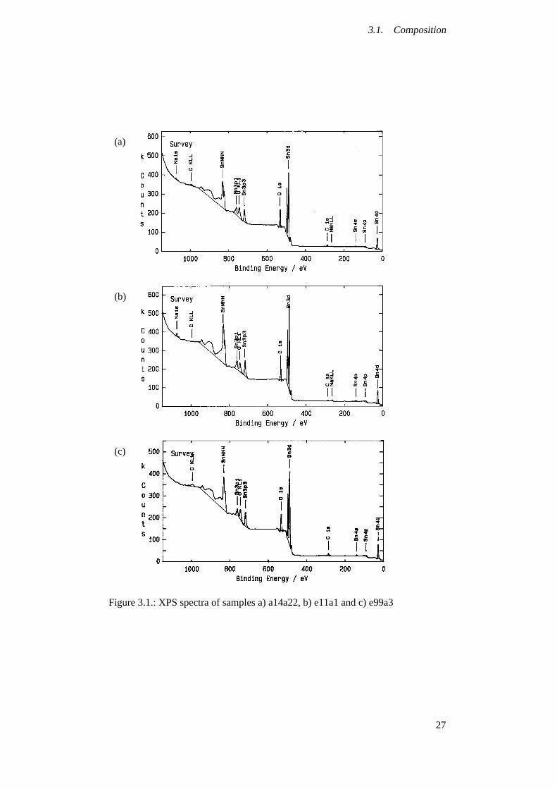


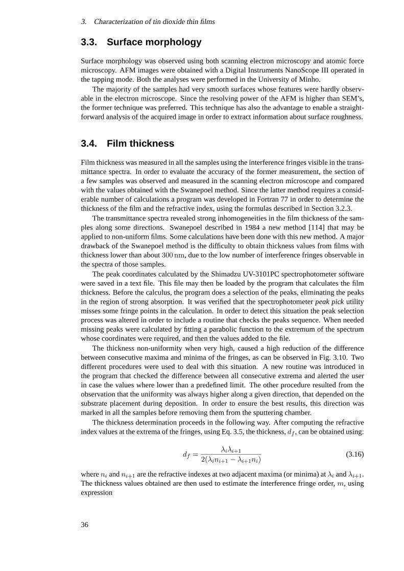


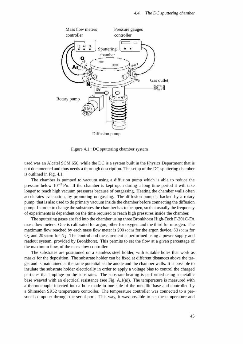


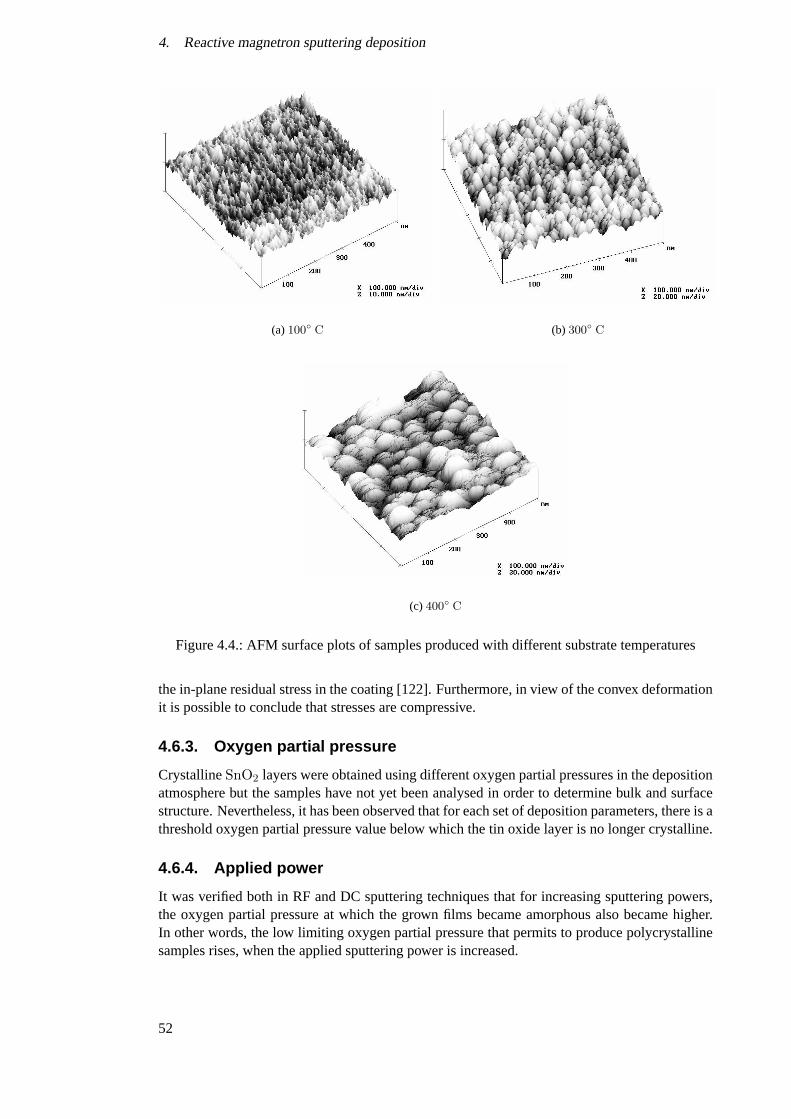

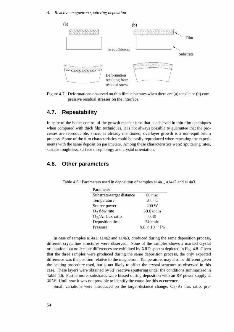
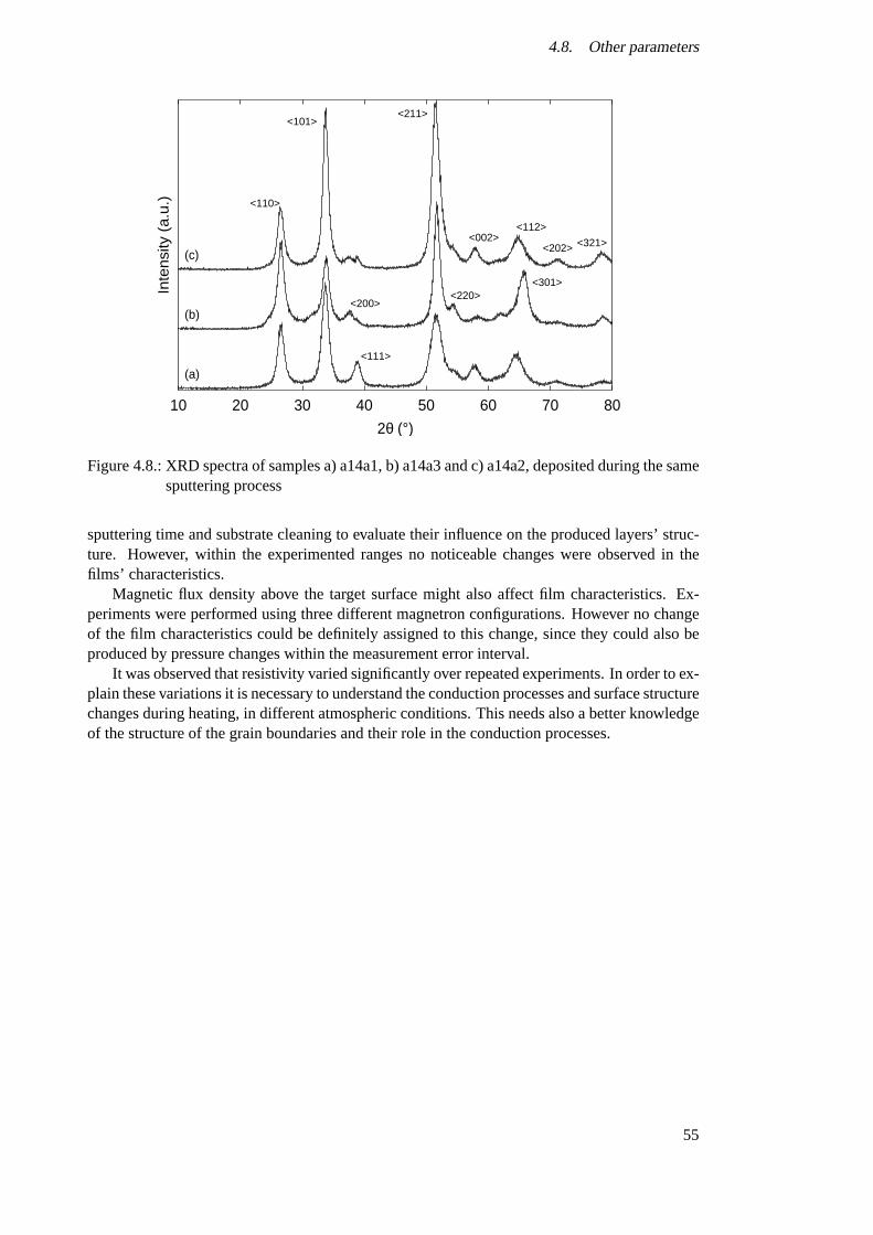


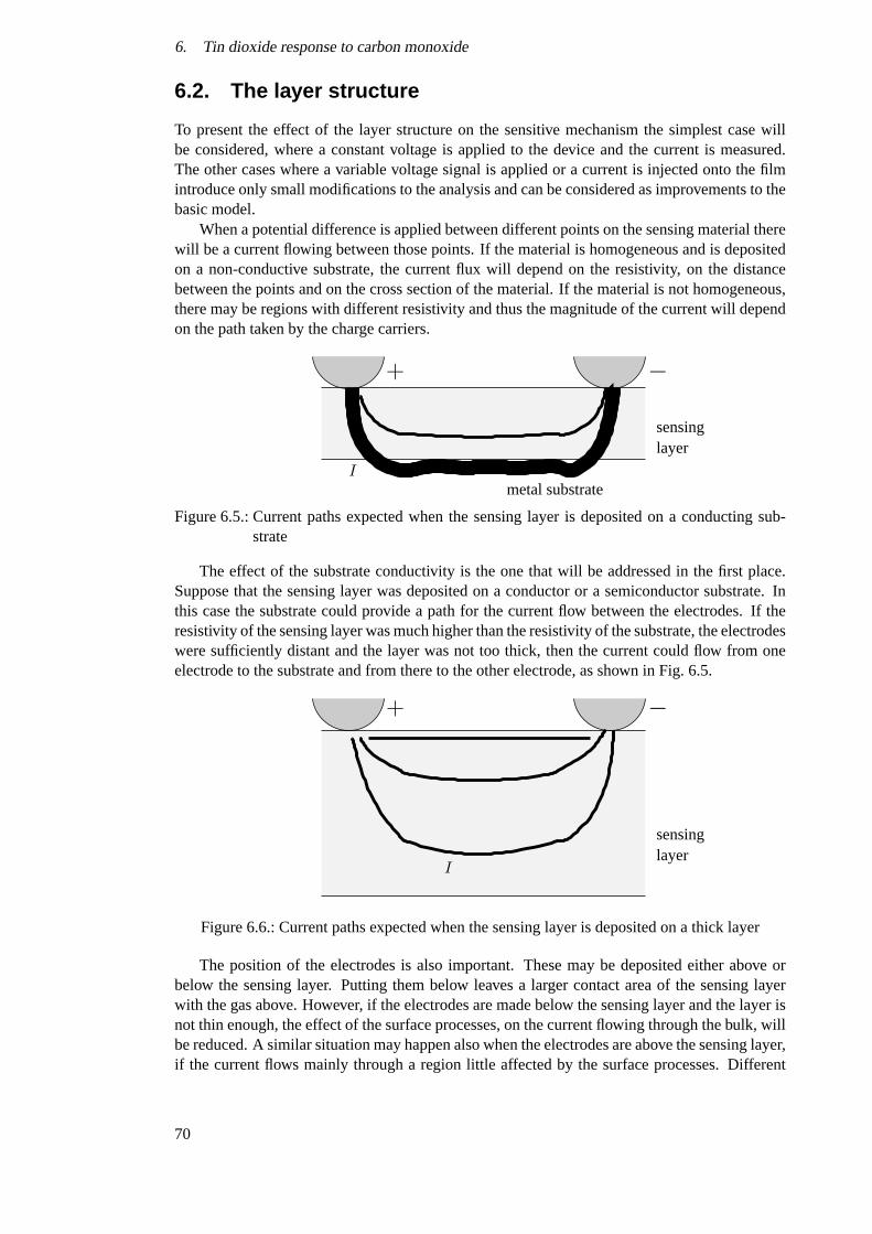


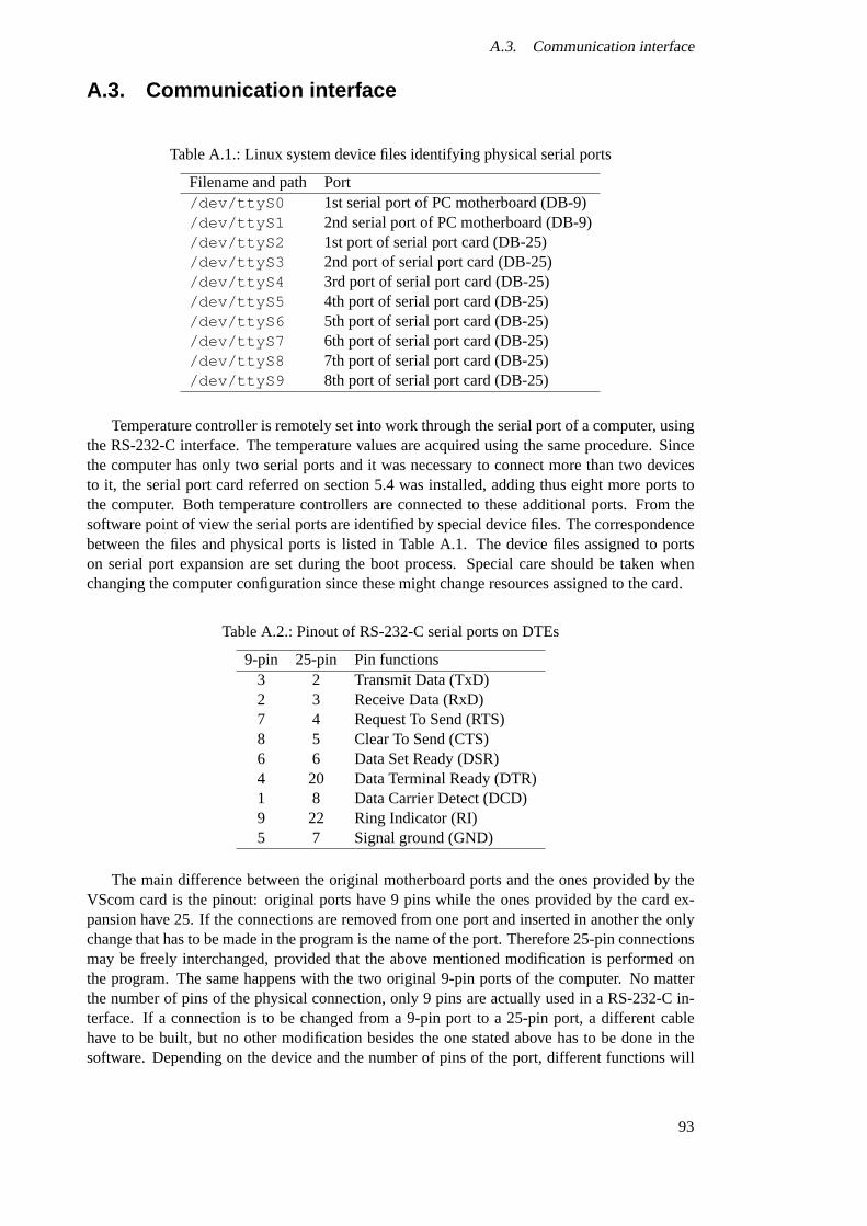
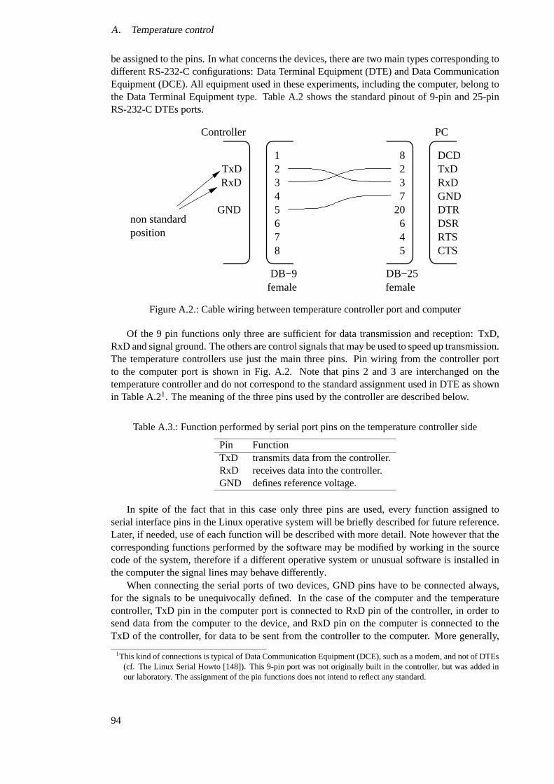


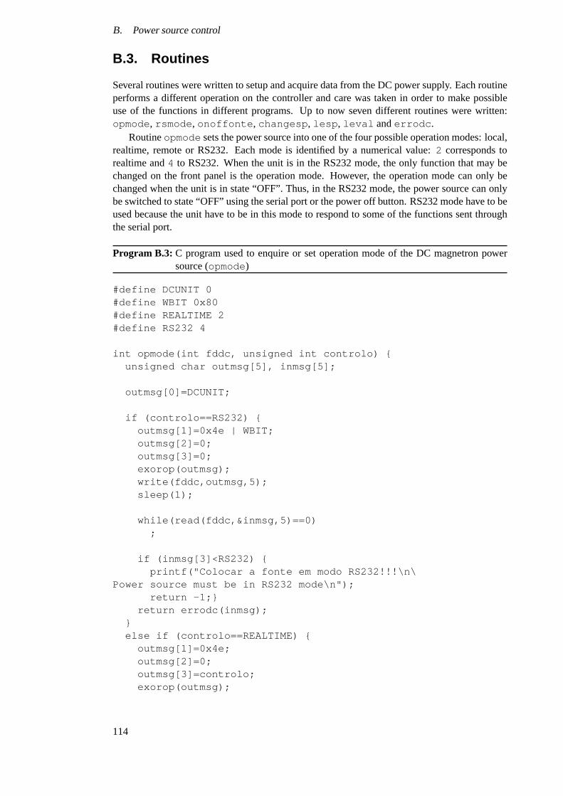


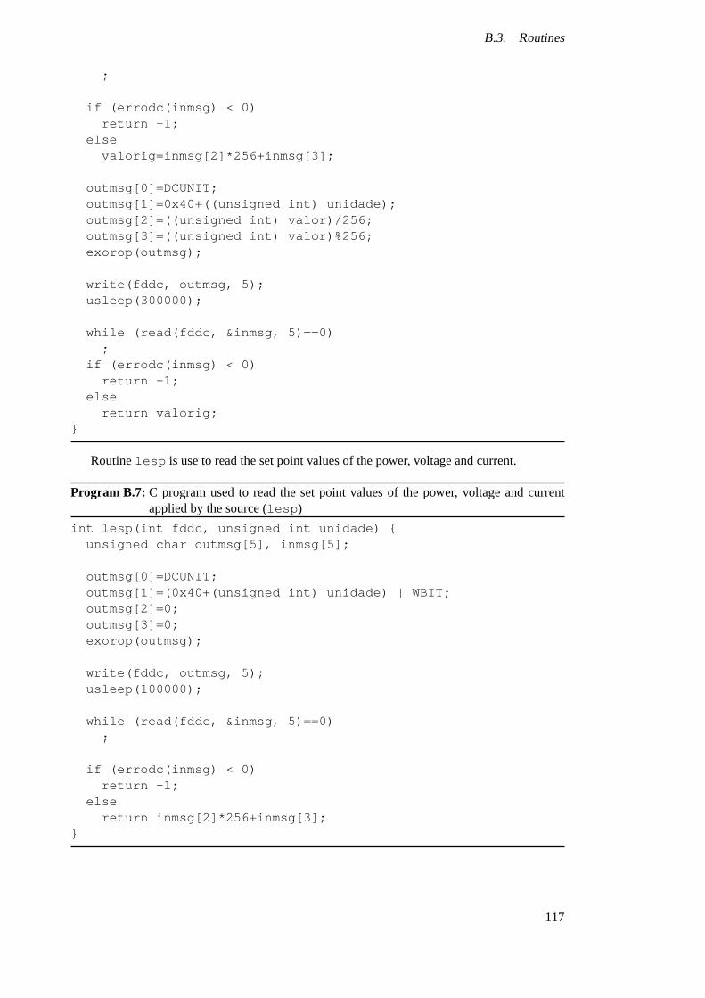


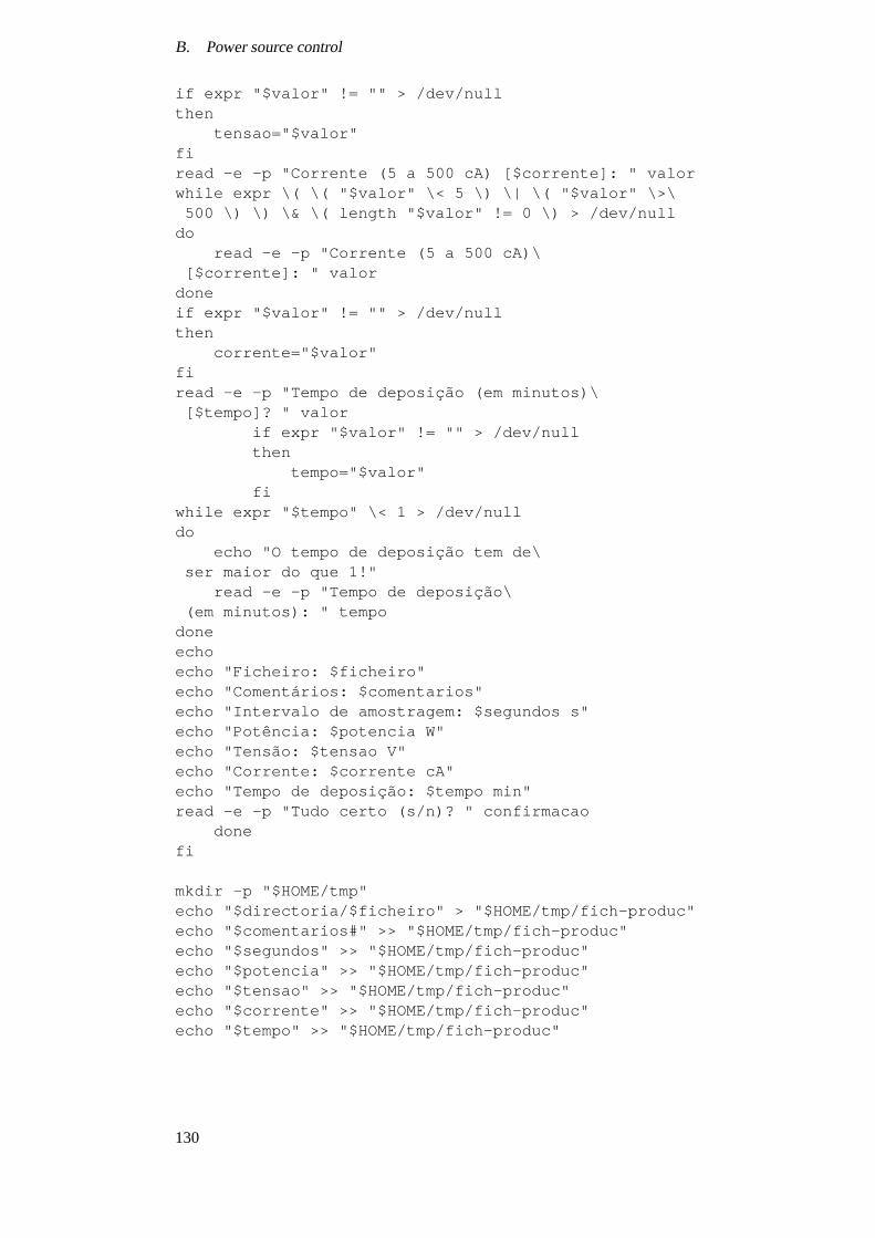
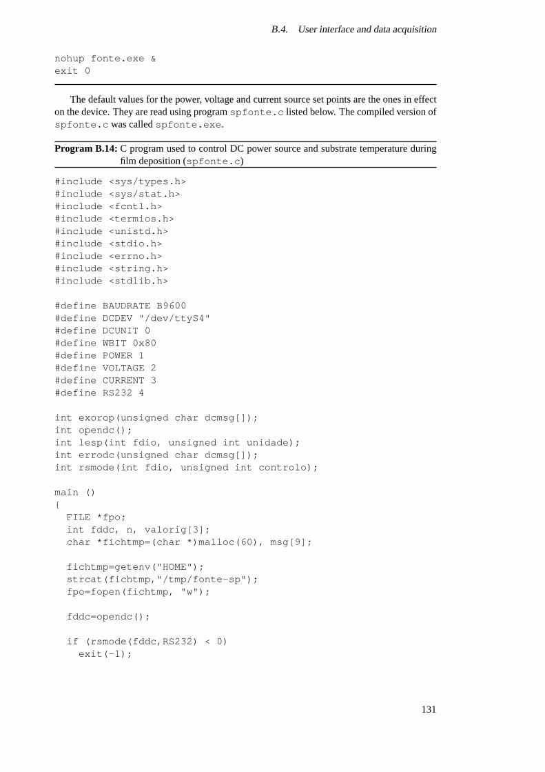


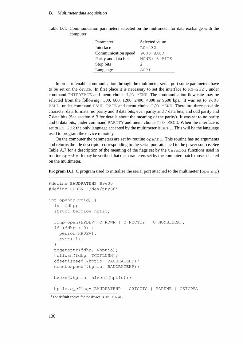


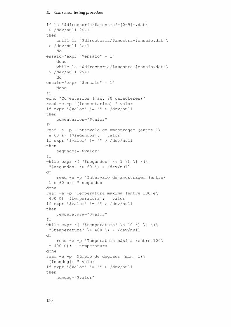
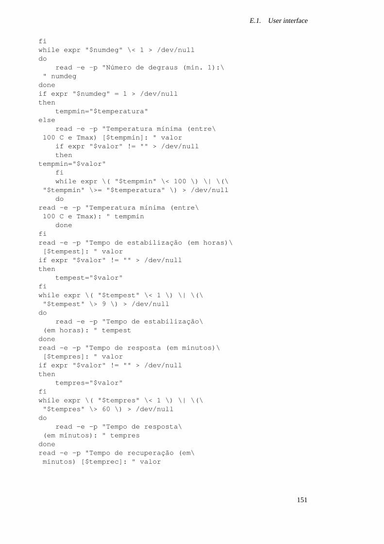


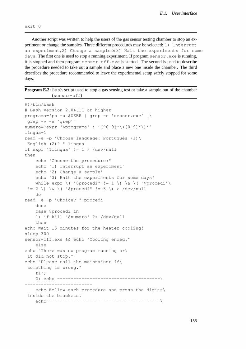


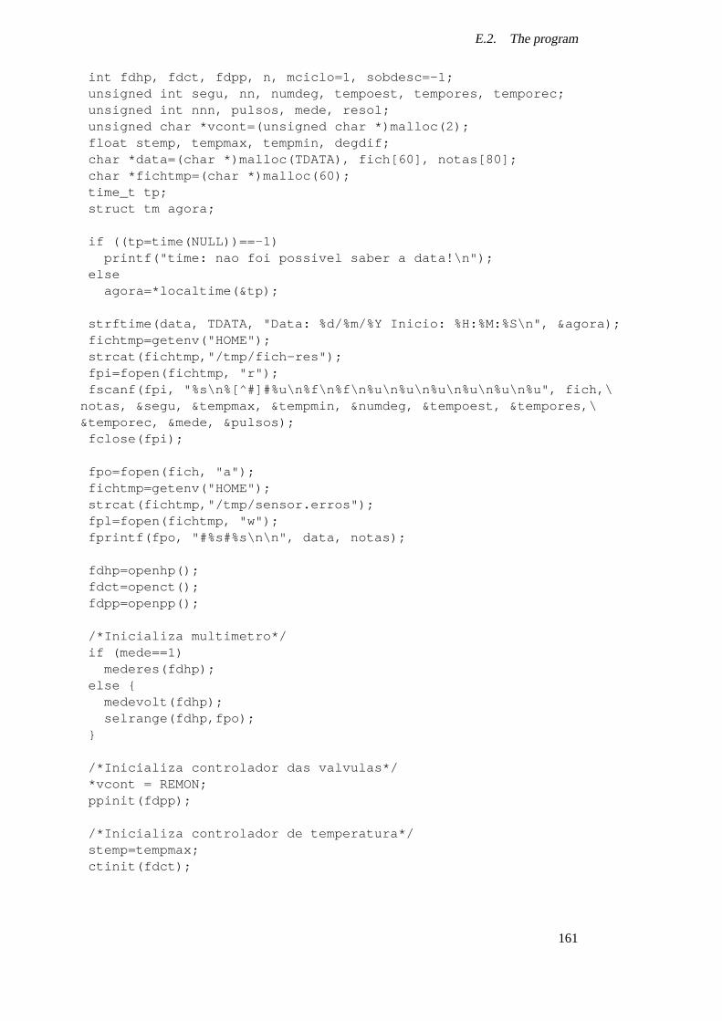


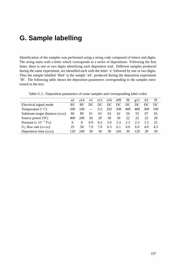


![[t0] TEORÍA DE LA INTEGRACIÓN CONCEPTUAL: UNA … · conceitual mostraram as relações cognitivas que se apresentavam. Porém as diferenças geracionais dos participantes, se estabeleceram](https://static.documents.pub/doc/80x56/5c45822993f3c34c4658cf99/t0-teoria-de-la-integracion-conceptual-una-conceitual-mostraram-as-relacoes.jpg)


