Page 1
1
"This accepted author manuscript is copyrighted and published by Elsevier. It is posted
here by agreement between Elsevier and MTA. The definitive version of the text was
subsequently published in [Nuclear Instruments and Methods in Physics Research A
832 (2016) 254–258; DOI 10.1016/j.nima.2016.06.132]. Available under license CC-BY-
NC-ND."
Page 2
2
Coating and functionalization of high density ion track structures by atomic layer
deposition
Laura Mättö1, Imre M. Szilagyi
2,3,4*, Mikko Laitinen
1, Mikko Ritala
4, Markku Leskelä
4, Timo
Sajavaara1
1Department of Physics, University of Jyväskylä, P.O. Box 35 (YFL), FI-40014, Finland
2Department of Inorganic and Analytical Chemistry, Budapest University of Technology and
Economics, Budapest, Szent Gellért tér 4, H-1111, Hungary
3MTA-BME Technical Analytical Research Group, Budapest, Szent Gellért tér 4, H-1111,
Hungary
4Department of Chemistry, University of Helsinki, Helsinki, P.O. Box 55, FI-00014, Finland
Email: [email protected]
Abstract
In this study flexible TiO2 coated porous Kapton membranes are presented having electron
multiplication properties. 800 nm crossing pores were fabricated into 50 m thick Kapton
membranes using ion track technology and chemical etching. Consecutively, 50 nm TiO2
films were deposited into the pores of the Kapton membranes by atomic layer deposition
using Ti(iOPr)4 and water as precursors at 250 °C. The TiO2 films and coated membranes
were studied by scanning electron microscopy (SEM), X-ray diffraction (XRD) and X-ray
reflectometry (XRR). Au metal electrode fabrication onto both sides of the coated foils was
achieved by electron beam evaporation. The electron multipliers were obtained by joining
Page 3
3
two coated membranes separated by a conductive spacer. The results show that electron
multiplication can be achieved using ALD-coated flexible ion track polymer foils.
Keywords: nanostructures, oxides, polymers, thin films, coatings, electrical properties
1. Introduction
Porous materials with precisely controlled properties, such as pore size and diameter, have
several applications in, for instance, filtration [1], gas sensing [2,3], catalysis [4],
photocatalysis [5,6], solar cells [7], adsorption [8,9], and biomedical research [10]. Micro-
channel plates (MCPs) are special member of these materials, in which a porous membrane is
composed of parallelly aligned or crossing tubes. An MCP is an array of miniature electron
multipliers that are each acting as a continuous dynode chain. They can be used e.g. in night
vision applications, photomultipliers, particle and time-of-flight detectors [11].
One method to fabricate porous films is to shoot single heavy energetic ions through a
material to be manipulated. In ion track method [12] these ions with typical energies of
several hundred MeVs are generated by means of an accelerator. When these ions hit the
target material, they lose their energy by various interactions with the material, and cause
excitation and ionization of target electrons (electronic energy loss), projectile excitation and
ionization, electron capture, elastic collisions with target atoms (nuclear energy loss) and
electromagnetic radiation. For high energy heavy ions the most significant process is the
electronic energy loss. The incident ions are chosen in such a way that the energy transfer to
the material is large. The electronic energy loss can be well described by the Bethe-Bloch
formula and the SRIM software [13]. The incident ion induces ionization and electric
Page 4
4
excitation, which in polymers predominantly breaks chemical bonds and a damaged ion track
forms.
After the ion irradiation the pore is created via chemical etching process. The shape of the
etched pore depends on the etch velocity of the bulk material Vb (etch rate of undamaged
material) and the etch velocity of track line Vt (etch rate along the track). Both depend on the
etching conditions and Vt is also influenced by the energy loss of the irradiated ions. Vt
increases with increasing energy loss due to higher damage along the ion track [14]. Size of
the pore varies with the etching time, as well as the pH and temperature of the solution.
Atomic layer deposition (ALD) is a gas phase thin film deposition method based on surface
controlled self-limiting reactions of volatile precursors, which are introduced into the reaction
chamber alternately. ALD can be used to coat not only flat substrates, but also complex
surfaces and highly porous materials with uniform films having thickness even down to
single nanometers [15,16]. These films can be, for instance, insulating oxides or conducting
metals, ternary compounds or polymers [17,18]. These features make ALD a convenient
choice for modifying the surface properties of various nanostructures [19-21] or even
sensitive substrates such as biomaterials [22].
In previous work by others, ion track structures and ALD have been combined to make
nanotubes after dissolving the soluble nano templates [23]. On the other hand, ALD has been
used to coat with thin films MCP structures made of glass [24], lead glass [25], borosilicate
glass [26,27], porous silicon [28] and anodized Al2O3 [29]. These ALD-MCP structures
showed mostly similar or even better properties than conventional MCPs based on lead glass,
and had increased gain and improved stability as a function of extracted charge in several
cases. However, all these substrates were rigid materials, and for MCP applications flexible
MCP structures might have obvious advantages in several fields (e.g. night vision). Also
MCP devices from plastic materials have been previously reported [30,31]. These devices
Page 5
5
were made out of porous polymethyl methacrylate (PMMA) having pore size and thickness
of 50 µm and 5 mm, respectively. The polymer channels had separate unspecified conductive
and emissive low-temperature ALD coatings. The electron yield was amplified with
additional conventional MCP stack after the polymer MCP. In ALD coated MCP structures
various secondary electron emissive layers were deposited, e.g. MgO, MgO/TiO2, TiO2, etc
[32]. Though TiO2 is a less common material for secondary electron emission, its easy ALD
deposition makes it a good candidate to prepare new MCP structures.
In this study ALD was used to grow TiO2 films on the sub-micron diameter ion track
structures in order to have low-resistivity and enhanced secondary electron production in the
pores. The idea was that an 16
O beam releases secondary electrons upon collision with the
pore walls. The secondary electron cloud can divide between crossing pores and further
increase the number of electrons. With high secondary electron gain, this type of structures
could act as low-cost electron multipliers in optical and various detector applications. The
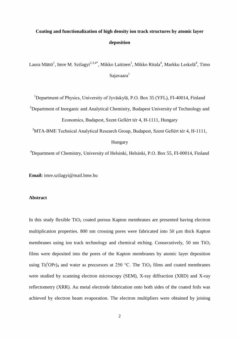
substrate for ALD in our case was a highly flexible porous ion track polyimide (Kapton) (Fig.
1).
2. Experimental
Self-supporting 50 µm thick polyimide foils (Kapton from DuPont) were used as substrate
material. The foils were irradiated using the JYFL K-130 cyclotron and Radiation Effects
Facility (RADEF) irradiation chamber. The used ion was 600 MeV Xe25+
, the fluence varied
from 107 to 10
9 ions/cm
2, and individual irradiations lasted from seconds to thirty minutes.
During the irradiations the beam homogeneity and flux were monitored. Irradiation angle was
continuously varied between ±15o and the foil was also rotated in order to get crossing ion
Page 6
6
tracks in all directions, and thereby minimizing the probability of wide pores due to adjacent
tracks.
The irradiated foils were etched in NaOCl solution [33]. The desired pH for the solution was
obtained by adding boric acid (H3BO3), and the pH was monitored before and after the
etching. The pH was 10.5 in the beginning and 9.9 after the etching had been completed. The
etching temperature was (60 ± 2 oC), and the etching time was 6 hours. The as-formed pores
were imaged using a scanning electron microscope (Hitachi S-4800 FE-SEM), and the pore
diameter was measured to be about 800 nm.
In order to both enhance the secondary electron production from the pore surface and make
the pore surface resistive, the porous foils were coated by atomic layer deposition with a TiO2
layer using TTIP (titanium tetraisopropoxide, 65 °C evaporation temperature) + H2O as
precursors at 250 °C. Each cycle had the following sequence: two times 0.5 s pulse and 1 s
purge followed by 0.5 pulse and 15 s purge for TTIP, then the same for H2O. Ca. 50 nm TiO2
was deposited in 1500 cycles in a Picosun Sunale R-150 ALD reactor.
The film thickness (47.7 nm) was determined by X-ray reflectometry (Bruker D8 Advance )
using a TiO2 film, which was deposited onto a 100 mm(100) Si wafer under the same
conditions as used for the Kapton membranes. The growth rate per cycle corresponds well to
the reported value 0.3 Å/cycle [34].
XRD pattern of the reference TiO2 film on Si substrate was recorded by a PANalytical X’pert
Pro MPD X-ray diffractometer using Cu K radiation and grazing incidence angle mode.
Consecutively, conducting 20 nm thick Au electrodes were electron beam evaporated on both
sides of the ALD coated porous foils in an ultra high vacuum (UHV) environment.
The electron multiplication properties of the prepared foils were studied using a specially
made setup (Fig. 2). The primary setup consisted of two coated 50 µm thick polyimide foils
which were separated by 2 mm conductive spacer ring. The voltage over the ALD-Kapton
Page 7
7
stack was evenly divided using two 1.2 MΩ resistors. The lower electrode had a fixed
potential of –1800 V and the potential of the upper electrode was varied between –1625 V
and –2000 V in order to study the electron multiplication. The weak signals from Kapton
electron multiplier were amplified by two conventional micro channel plates (MCP). The
upper electrode of the MCP was set to a potential of –1725 V.
The operation of the Kapton/TiO2 multipliers in ion detection was tested by backscattering a
4.8 MeV 16
O2+
beam from the Pelletron accelerator from a thin Au target towards the foils.
The energy of scattered 16
O ions was about 3.6 MeV, and the range in Kapton coated by 50
nm TiO2 is about 4.1 µm as calculated using SRIM. The measurement time for each point
was 500 s and the number of events was normalized using the incident ion fluence
information obtained from the beam chopper.
3. Results and discussion
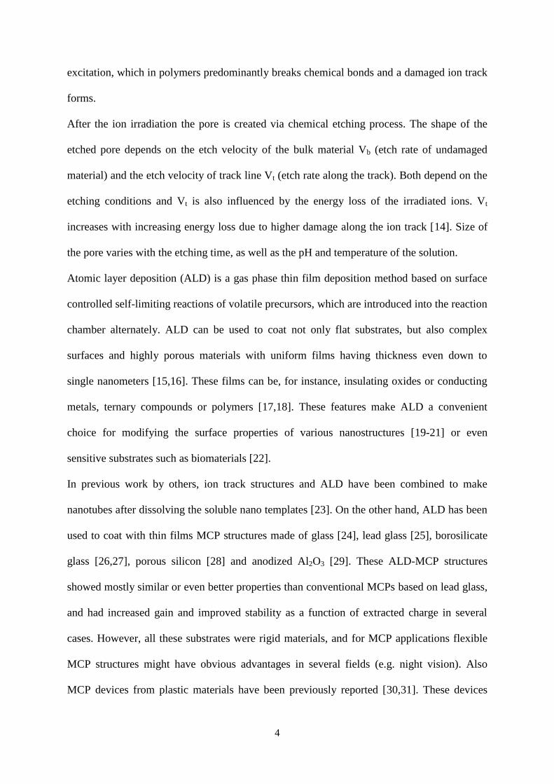
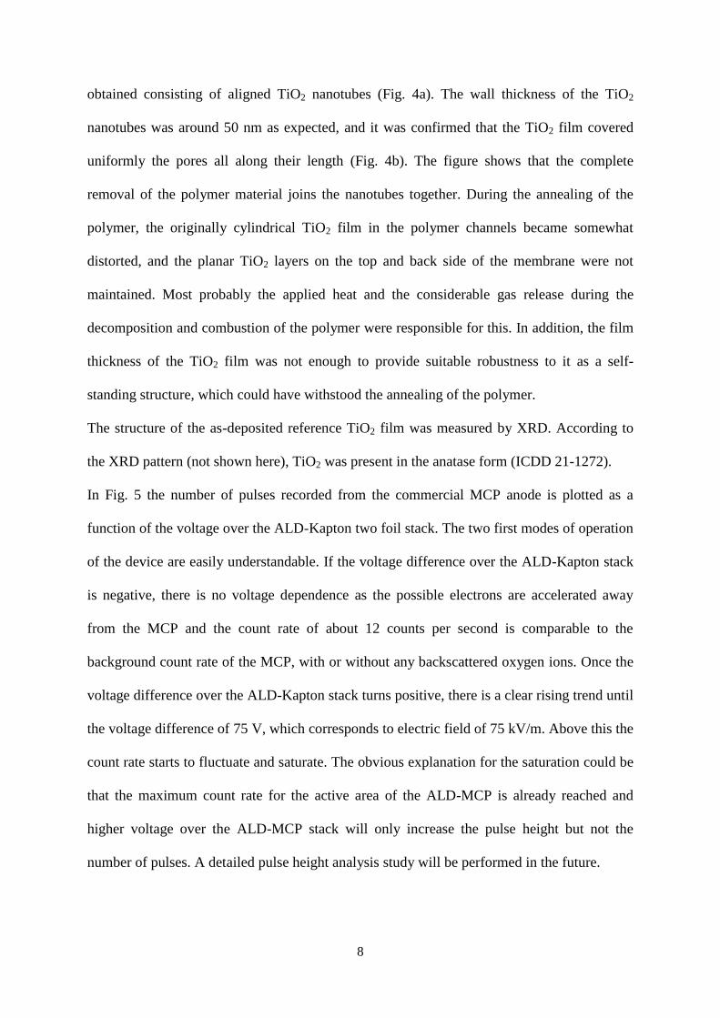
The deposition of the ALD TiO2 film was successful on polyimide even at a growth
temperature of 250 oC (Fig. 3). The 50 mm thick Kapton/TiO2 porous membrane had ca. 800
nm diameter channels penetrating through the whole structure (A/R = 62.5). The small cracks
visible on the TiO2 film on surface of the membrane are most likely due to polymer shrinkage
during the cooling down after the ALD growth. The thermal expansion coefficient of
polyimide is more than ten times higher than the one for TiO2. The good quality of coated
foils proves the compatibility of ion track technology using polyimide foils with the ALD
method even at fairly high deposition temperatures.
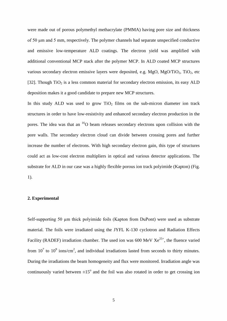
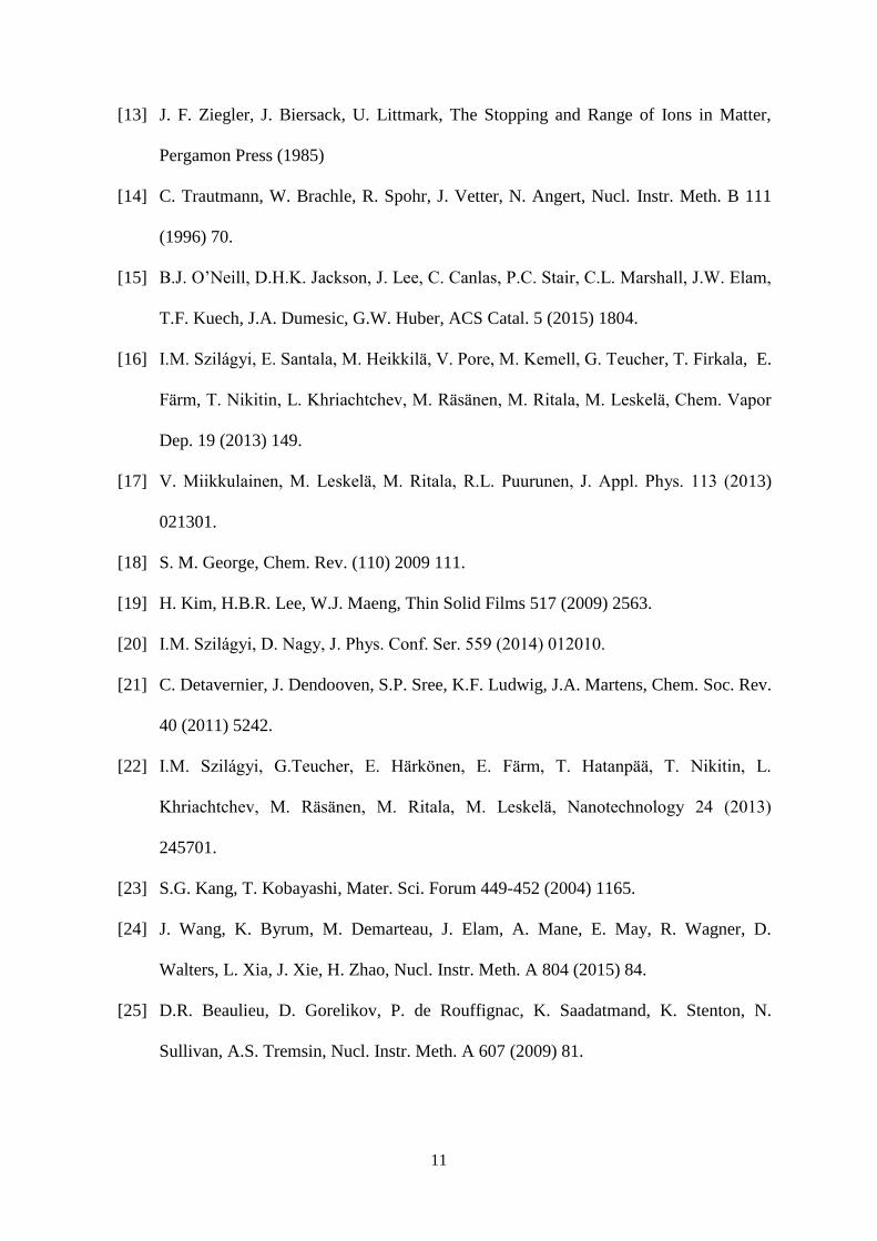
To check the conformality of the as-deposited TiO2 film, the coated membrane was annealed
in air using 1 °C/min heating rate up to 600 °C and then keeping the sample at 600 °C for an
hour. As a result of the polyimide membrane combustion a porous inorganic membrane was
Page 8
8
obtained consisting of aligned TiO2 nanotubes (Fig. 4a). The wall thickness of the TiO2
nanotubes was around 50 nm as expected, and it was confirmed that the TiO2 film covered
uniformly the pores all along their length (Fig. 4b). The figure shows that the complete
removal of the polymer material joins the nanotubes together. During the annealing of the
polymer, the originally cylindrical TiO2 film in the polymer channels became somewhat
distorted, and the planar TiO2 layers on the top and back side of the membrane were not
maintained. Most probably the applied heat and the considerable gas release during the
decomposition and combustion of the polymer were responsible for this. In addition, the film
thickness of the TiO2 film was not enough to provide suitable robustness to it as a self-
standing structure, which could have withstood the annealing of the polymer.
The structure of the as-deposited reference TiO2 film was measured by XRD. According to
the XRD pattern (not shown here), TiO2 was present in the anatase form (ICDD 21-1272).
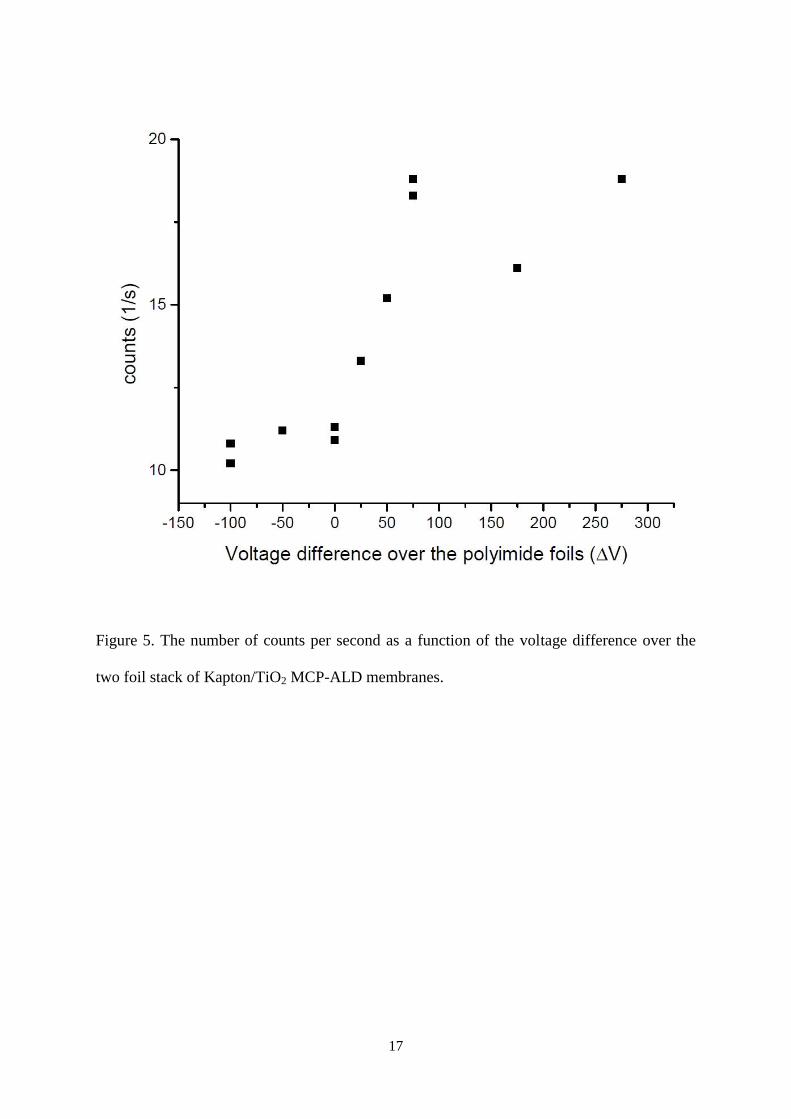
In Fig. 5 the number of pulses recorded from the commercial MCP anode is plotted as a
function of the voltage over the ALD-Kapton two foil stack. The two first modes of operation
of the device are easily understandable. If the voltage difference over the ALD-Kapton stack
is negative, there is no voltage dependence as the possible electrons are accelerated away
from the MCP and the count rate of about 12 counts per second is comparable to the
background count rate of the MCP, with or without any backscattered oxygen ions. Once the
voltage difference over the ALD-Kapton stack turns positive, there is a clear rising trend until
the voltage difference of 75 V, which corresponds to electric field of 75 kV/m. Above this the
count rate starts to fluctuate and saturate. The obvious explanation for the saturation could be
that the maximum count rate for the active area of the ALD-MCP is already reached and
higher voltage over the ALD-MCP stack will only increase the pulse height but not the
number of pulses. A detailed pulse height analysis study will be performed in the future.
Page 9
9
The electron multiplication is not only dependent on the secondary electron production
capability of the pore surface material but also on the electron energy. The flight path is
longer and therefore also the energy of the electrons is higher for greater pore diameter and it
could be that the 800 nm pore diameter these foils had is quite close to the diameter below
which electrons do not get enough energy before colliding with the wall to multiply the yield.
On the other hand, smaller pore diameter gives better spatial and temporal resolution. One
special signal enhancing new property these ion track foils have is due to the crossing of the
pores inside the polymer. The electrons can find their way to another pore and generate a
strong daughter signal there as well.
4. Conclusions
In this study we have demonstrated the ability to combine ion track technology and ALD in
fabrication of films with electron multiplication properties. 50 nm TiO2 films were deposited
onto 50 m Kapton foils, which had 800 nm crossing pores prepared previously by ion track
method and chemical etching. The results show that electron multiplication can be achieved
using the ALD-coated flexible ion track foils, although multiplication is not still strong
enough for direct detection, and thus an extra amplification stage is needed, and further
studies are required in finding the optimal pore diameter and ALD film thickness.
One additional possibility for applications opens when the supporting organic polymer is
etched away like is shown in Fig. 3a, where an array of 800 nm wide TiO2 nanotubes with 50
nm wall thickness film is prepared after annealing at 600 °C in air. Due to the crossing tracks,
the structure is still rigid and could be used as a highly porous substrate in, for instance, cell
growth studies or catalysis.
Page 10
10
Acknowledgements
This work was supported under the auspices of Finnish Centre of Excellence Programme
(Project No. 213503, 251353 Nuclear and Accelerator Based Physics). I.M.S. thanks for a
Marie Curie Intra-European Fellowship (PIEF-GA-2009-235655), an OTKA-PD-109129
grant and a János Bolyai Research Fellowship of the Hungarian Academy of Sciences.
References
[1] E.C. Hammel, O.L.R. Ighodaro, O.I. Okoli, Ceram. Int. 40 (2014) 1535.
[2] C. RoyChaudhuri, Sens. Actuat. B 210 (2015) 310.
[3] R.V. Godbole, P. Rao, P.S. Alegaonkar, S. Bhagwat, Mater. Chem. Phys. 161 (2015)
135.
[4] H.J. Jeong, J. W. Kim, D.Y. Jang, J.H. Shim, J. Power Sources 291 (2015) 239.
[5] Kocakusakoglu, M. Daglar, M. Konyar, H.C. Yatmaz, K. Öztürk, J. Eur. Ceram. Soc.
35 (2015) 2845.
[6] O. Czakkel, E. Geissler, I.M. Szilágyi, K. László, Nanomat. Environ. 1 (2013) 23.
[7] Lim, D.Y. Lee, S.A. Patil, N.K. Shrestha, S.H. Kang, Y.C. Nah, W. Lee, S.H. Han,
Mater. Chem. Phys. 148 (2014) 562.
[8] S. Gadipelli, Z.X. Guo, Prog. Mater. Sci. 69 (2015) 1.
[9] O. Czakkel, E. Geissler, I.M. Szilágyi, E Székely, K. László, J. Coll. Interface Sci.
337 (2009) 513.
[10] X. Du, S.Z. Qiao, Small, 11 (2015), 392.
[11] T. Gys, Nucl. Instr. Meth. A 787 (2015) 254.
[12] C. Trautmann, S. Bouffard, R. Spohr, Nucl. Instr. Meth. B 116 (1996) 429.
Page 11
11
[13] J. F. Ziegler, J. Biersack, U. Littmark, The Stopping and Range of Ions in Matter,
Pergamon Press (1985)
[14] C. Trautmann, W. Brachle, R. Spohr, J. Vetter, N. Angert, Nucl. Instr. Meth. B 111
(1996) 70.
[15] B.J. O’Neill, D.H.K. Jackson, J. Lee, C. Canlas, P.C. Stair, C.L. Marshall, J.W. Elam,
T.F. Kuech, J.A. Dumesic, G.W. Huber, ACS Catal. 5 (2015) 1804.
[16] I.M. Szilágyi, E. Santala, M. Heikkilä, V. Pore, M. Kemell, G. Teucher, T. Firkala, E.
Färm, T. Nikitin, L. Khriachtchev, M. Räsänen, M. Ritala, M. Leskelä, Chem. Vapor
Dep. 19 (2013) 149.
[17] V. Miikkulainen, M. Leskelä, M. Ritala, R.L. Puurunen, J. Appl. Phys. 113 (2013)
021301.
[18] S. M. George, Chem. Rev. (110) 2009 111.
[19] H. Kim, H.B.R. Lee, W.J. Maeng, Thin Solid Films 517 (2009) 2563.
[20] I.M. Szilágyi, D. Nagy, J. Phys. Conf. Ser. 559 (2014) 012010.
[21] C. Detavernier, J. Dendooven, S.P. Sree, K.F. Ludwig, J.A. Martens, Chem. Soc. Rev.
40 (2011) 5242.
[22] I.M. Szilágyi, G.Teucher, E. Härkönen, E. Färm, T. Hatanpää, T. Nikitin, L.
Khriachtchev, M. Räsänen, M. Ritala, M. Leskelä, Nanotechnology 24 (2013)
245701.
[23] S.G. Kang, T. Kobayashi, Mater. Sci. Forum 449-452 (2004) 1165.
[24] J. Wang, K. Byrum, M. Demarteau, J. Elam, A. Mane, E. May, R. Wagner, D.
Walters, L. Xia, J. Xie, H. Zhao, Nucl. Instr. Meth. A 804 (2015) 84.
[25] D.R. Beaulieu, D. Gorelikov, P. de Rouffignac, K. Saadatmand, K. Stenton, N.
Sullivan, A.S. Tremsin, Nucl. Instr. Meth. A 607 (2009) 81.
Page 12
12
[26] O.H.W. Siegmund, J.B. McPhate, A.S. Tremsin, S.R. Jelinsky, R. Hemphill, H.J.
Frisch, J. Elam, A. Mane, Nucl. Instr. Meth. A 695 (2012) 168.
[27] J. Xie, K. Byrum, M. Demarteau, E. May, R. Wagner, D. Walters, J. Wang, L. Xia, H.
Zhao, Nucl. Instr. Meth. A 824 (2016) 159.
[28] Franco, Y. Riesen, N. Wyrsch, S. Dunand, F. Powolny, P. Jarron, C. Ballif, Nucl.
Instr. Meth. A 695 (2012) 74.
[29] G. Drobychev, A. Barysevich, K. Delendik, A. Karneyeu, P. Nédélec, D. Sillou, O.
Voitik, Nucl. Instr. Meth. A 567 (2006) 290.
[30] D.R. Beaulieu, D. Gorelikov, H. Klotzsch, P. de Rouffignac, K. Saadatmand, K.
Stenton, N. Sullivan, A.S. Tremsin, Nucl. Instr. Meth. A 633 (2011) S59,
[31] D. Beaulieu, D. Gorelikov, H. Klotzsch, J. Legere, J. Ryan, P. de Rouffignac, K.
Saadatmand, K. Stenton, N. Sullivan, A. Tremsin, Nucl. Instr. Meth. A 659 (2011)
394.
[32] S.J. Jokela , I.V. Veryovkin, A.V. Zinovev, J.W. Elam, A.U. Mane, Q. Peng, Z.
Insepov, Phys. Proc. 37 (2012) 740.
[33] Z. Tian-Cheng, R. Brandt, P. Vater, J. Vetter, Nucl. Tracks Radiat. Measur. 15 (1988)
771.
[34] M. Ritala, M. Leskelä, L. Niinistö, P. Haussalo, Chem. Mater. 5 (1993) 1174.
Page 13
13
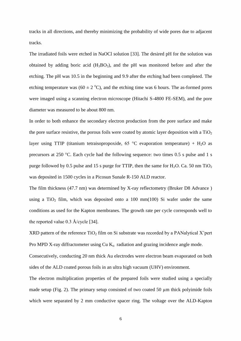
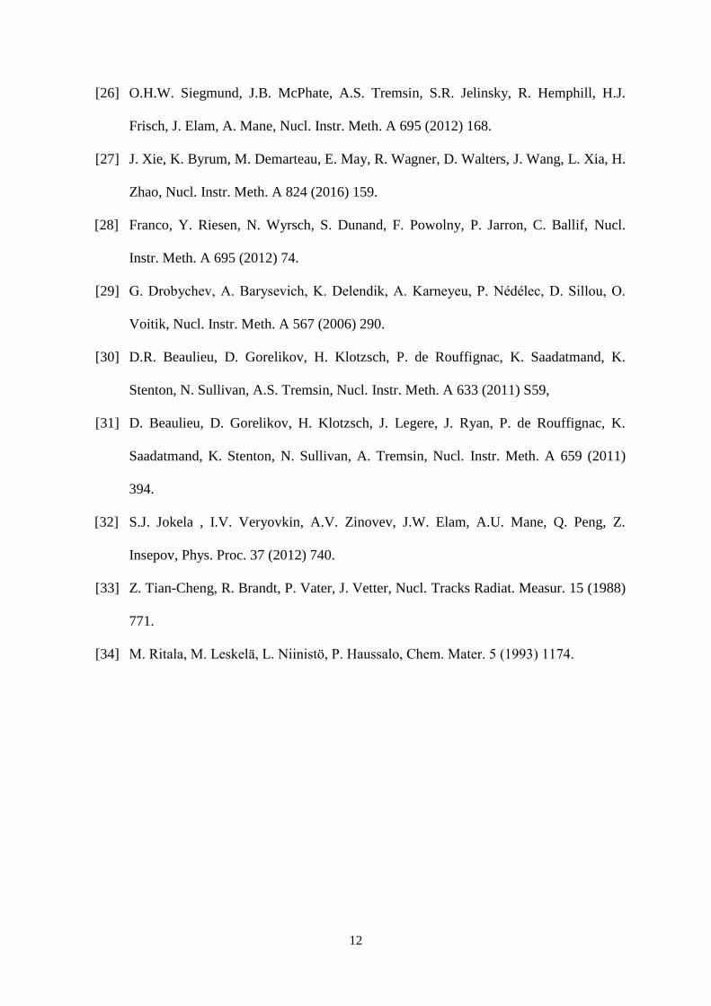
Figure. 1. A) Schematic diagram of the electron multiplier detector configuration. 1) 3,6 MeV
16O beam and aluminum collimator 2) porous polyimide foil 3) standard MCP used for post
amplification of electron signal and 4) charge collecting plate. B) Polyimide foil thickness
was 50 µm and pore diameter 800 nm. During the irradiation the foil was tilted between 0
and 15 degrees. C) The ion beam releases secondary electrons upon collision with the pore
walls. The secondary electron cloud can divide between crossing pores and further increase
the number of electrons.
Page 14
14
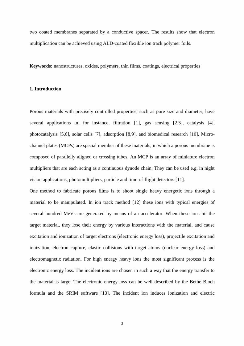
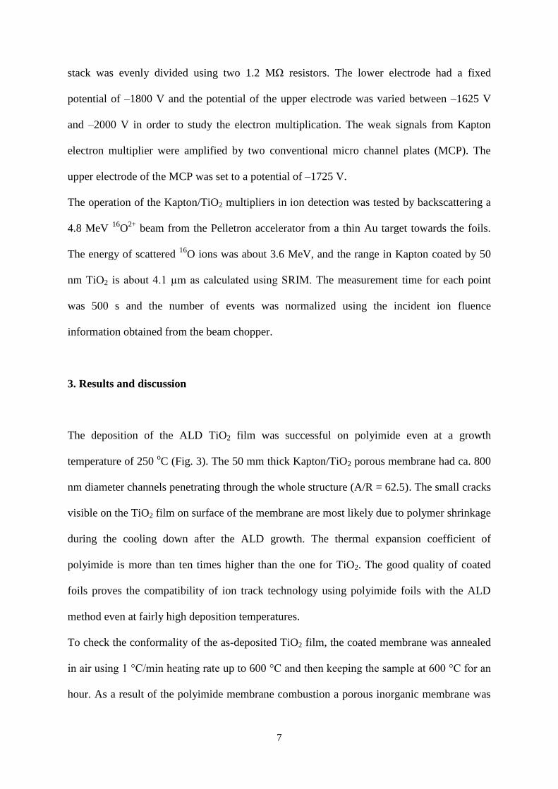
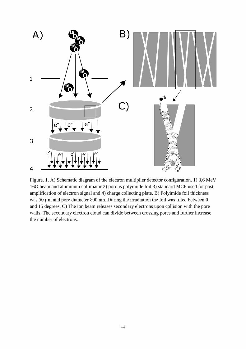
Figure 2. A) A photograph of the used setup showing the collimated entrance to the
Kapton/TiO2 MCP-ALD two foil stack where the scattered 3.6 MeV oxygen beam hits. In B)
the same setup is shown from the opposite direction showing the stack and its top and lower
contacts as well as the commercial MCP stack which was used to amplify the signal behind
the metal plate.
Page 15
15
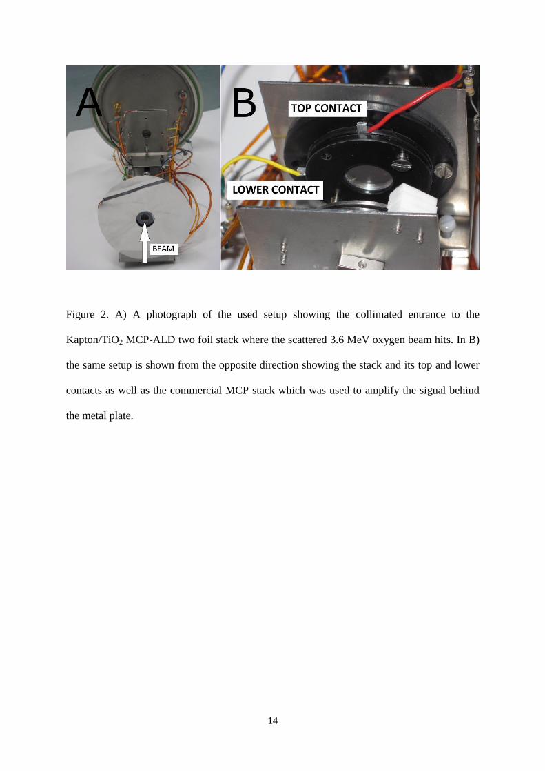
Figure 3. SEM image of the TiO2 coated porous Kapton membrane. A 50 µm polyimide foil
was irradiated with 600 MeV Xe ions and etched for 6 hours in sodium hypocloride and boric
acid solutions having pH 10.5. After etching a 50 nm ALD-TiO2 film was deposited on both
sides but also on the pore inner surfaces. The final pore diameter was about 800 nm. The
small cracks on the TiO2 film are most likely due to polymer shrinkage during the cooling
down after the ALD growth.
Page 16
16
Figure 4. Self-supporting porous ALD TiO2 membrane after removal of the polyimide
substrate by annealing in air at 600 °C.
Page 17
17
Figure 5. The number of counts per second as a function of the voltage difference over the
two foil stack of Kapton/TiO2 MCP-ALD membranes.