96


Contents About this course 5
1. Introduction 6 1.1 Audio frequencies 6
1.2 Digital audio 7
1.2.1 Analogue vs digital signals 7 1.2.2 Sampling 7
1.2.3 Aliasing 8 1.2.4 Nyquist sampling theorem 8
1.3 Analogue to digital conversion 8 1.3.1 The AD7680 ADC 9
1.4 Digital to analogue conversion 10
1.4.1 The AD5662 DAC 11 2. Program 1 Laying the foundations 12
2.1 Introduction 12 2.2 Objective 12
2.3 Requirements 12
2.4 Flowcode program outline 12 2.5 The system components 12
2.5.1 The DSP System component 13 2.5.2 The DSP Input component 13
2.5.3 The DSP Output component 13
2.5.4 The SPI component 13 2.5.5 The graphical LCD component 13
2.6 Creating the program 14 2.6.1 The Dashboard panel 14
2.6.2 The flowchart 15 2.6.3 The hardware 16
2.6.4 Testing 16
2.6.5 The Flowcode program in detail 17 2.7 Further work 18
3 Digital signal processing 19 3.1 The dsPIC microcontroller 19
3.1.1 What is a microcontroller 19
3.1.2 Differences between dsPIC and PIC 19 3.1.3 Dynamic pipelining 21
3.1.4 Other DSP features 21 4. Program 2 - Adding an echo 26
4.1 Introduction 26 4.2 Objective 26
4.3 Requirements 26
4.4 Flowcode program outline 26 4.5 The system components 27
4.5.1 The DSP Scale component 27 4.5.2 The DSP Sum component 27
4.5.3 The DSP Delay component 27
4.6 Creating the program 28 4.6.1 The dashboard panel 28
4.6.2 The flowchart 30 4.6.3 The hardware 31
4.6.4 Testing 31 4.6.5 The flowcode program in detail 32
4.7 Further work 32
5. DSP Communications 33 5.1 Communication options 33
5.2 What is SPI? 33 5.2.1 Three wire SPI 34
5.2.2 Four wire SPI 34
5.3 What is I2C? 35 5.4 What is a UART? 36

5.4.1 What's in a name? 36
5.4.2 Typical UART 36
5.4.3 UART frame 37 6. Program 3 - Reverberation 38
6.1 Introduction 38 6.2 Objective 38
6.3 Requirements 38
6.4 Flowcode program outline 38 6.5 The system components 39
6.5.1 The first DSP Scale component 39 6.5.2 The DSP Sum component 39
6.5.3 The DSP Delay component 39
6.5.4 The second DSP Scale component 39 6.6 Creating the program 40
6.6.1 The dashboard panel 40 6.6.2 The flowchart 42
6.6.3 The hardware 43 6.6.4 Testing 43
6.6.5 The flowcode program in detail 44
6.7 Further work 44 7. Signals and waveforms 45
7.1 Noise 46 7.2 Signal waveforms 47
8. Program 4 - Sine wave generator 48
8.1 Introduction 48 8.2 Objective 48
8.3 Requirements 48 8.4 Flowcode program outline 48
8.5 The system components 48 8.5.1 The Frequency generator component 49
8.5.2 The DSP Scale component 50
8.5.3 The switches 50 8.6 Creating the program 50
8.6.1 The dashboard panel 50 8.6.2 The flowchart 52
8.6.3 The hardware 54
8.6.4 Testing 54 8.6.5 The flowcode program in detail 56
8.7 Further work 56 9. Program 5 - Waveform generator 57
9.1 Introduction 57
9.2 Objective 57 9.3 Requirements 57
9.4 Flowcode program outline 57 9.5 The system components 58
9.5.1 The Frequency generator components 58 9.6 Creating the program 58
9.6.1 The dashboard panel 59
9.6.2 The flowchart 61 9.6.3 The hardware 62
9.6.4 Testing 62 9.6.5 The flowcode program in detail 63
9.7 Further work 63
10. Filters 64 10.1 Types of filter 64
10.2 Filter action 65 10.3 Filter properties 66
10.4 Filter problems 67 11. Program 6 - Low pass filter 68
11.1 Introduction 68

11.2 Objective 68
11.3 Requirements 68
11.4 Flowcode program outline 68 11.5 The system components 69
11.5.1 The DSP Filter component 69 11.5.2 The switches 69
11.6 Creating the program 70
11.6.1 The dashboard panel 70 11.6.2 The flowchart 71
11.6.3 The hardware 72 11.6.4 Testing 73
11.6.5 The flowcode program in detail 73
11.7 Further work 74 12. Digital filters 75
12.1 Analogue versus digital filters 75 12.2 Digital filters 75
12.2.1 Implementing digital filters 76 13. Program 7 - High pass filter 77
13.1 Introduction 77
13.2 Objective 77 13.3 Requirements 77
13.4 Flowcode program outline 77 13.5 The system components 77
13.5.1 The DSP Filter component 78
13.5.2 The switches 78 13.6 Creating the program 78
13.6.1 The dashboard panel 78 13.6.2 The flowchart 80
13.6.3 The hardware 81 13.6.4 Testing 81
13.6.5 The flowcode program in detail 82
13.7 Further work 82

About this course
Aims:
The principal aim of the course is to enable you to use Flowcode 6 (or later) to program the dsPIC microcontroller. The examples focus largely on using this microcontroller in digital audio applications.
On completing this course you will have learned: the fundamentals of audio digital processing; the functionality of the Matrix dsPIC hardware; techniques to program the dsPIC microcontroller to process audio signals; the commands and syntax used to input, process and output audio signals.
What you will need:
To complete this course you will need the following equipment:
Flowcode 6 (or later) software
E-blocks including: a dsPIC programmer (EB091)
a DSP Input E-block (EB085)
a DSP Output E-block (EB086)
a Switch unit E-block (EB007)
a Graphical LCD E-Block (EB084)
a high impedance microphone and earpiece
a universal power supply (HP2666)
Using this course:
This course presents you with a number of tasks detailed in the following text. All the information you need to complete them is contained in the notes.
Before starting any exercise, you are advised to spend time familiarising yourself with the information contained in the course, so that you know where to look when you get stuck. Time: If you undertake all of the exercises on this course then it will take you between twelve and sixteen hours.
1. Introduction
Digital signal processing (DSP) is used in a variety of areas, many related to audio and video production. Its uses include:
the enhancement of visual images;
the synthesis of sounds;
speech recognition;
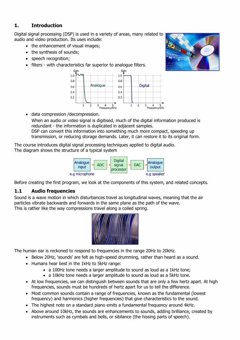
filters - with characteristics far superior to analogue filters.
data compression /decompression.
When an audio or video signal is digitised, much of the digital information produced is redundant - the information is duplicated in adjacent samples.
DSP can convert this information into something much more compact, speeding up transmission, or reducing storage demands. Later, it can restore it to its original form.
The course introduces digital signal processing techniques applied to digital audio. The diagram shows the structure of a typical system Before creating the first program, we look at the components of this system, and related concepts.
1.1 Audio frequencies
Sound is a wave motion in which disturbances travel as longitudinal waves, meaning that the air particles vibrate backwards and forwards in the same plane as the path of the wave. This is rather like the way compressions travel along a coiled spring.
The human ear is reckoned to respond to frequencies in the range 20Hz to 20kHz.
Below 20Hz, 'sounds' are felt as high-speed drumming, rather than heard as a sound.
Humans hear best in the 1kHz to 5kHz range:
a 100Hz tone needs a larger amplitude to sound as loud as a 1kHz tone; a 10kHz tone needs a larger amplitude to sound as loud as a 5kHz tone.
At low frequencies, we can distinguish between sounds that are only a few hertz apart. At high frequencies, sounds must be hundreds of hertz apart for us to tell the difference.
Most common sounds contain a range of frequencies, known as the fundamental (lowest frequency) and harmonics (higher frequencies) that give characteristics to the sound.
The highest note on a standard piano emits a fundamental frequency around 4kHz.
Above around 10kHz, the sounds are enhancements to sounds, adding brilliance, created by instruments such as cymbals and bells, or sibilance (the hissing parts of speech).

1.2 Digital audio
Digital audio techniques have largely replaced analogue processes in audio and video engineering - CD's replaced vinyl discs; DVD's replaced videotape; music synthesisers went from analogue to digital. Before we look at digital processing techniques, we need to know what a digital signal is.
1.2.1 Analogue vs digital signals
An analogue signal is an electrical copy (analogy) of a natural effect, such as a sound wave, a light wave, or a pressure variation. As these vary continuously in size, so the analogue electrical signal varies in voltage (usually), having any value of voltage within the range of the system’s power supply voltage. It can be precise copy of the process it represents.
Digital signals are sequences of numerical information about the process. For electrical simplicity, they rely on the binary number system - a string of 0’s and 1’s. These are represented by specific voltage levels within the electronic system. For example, with a power supply voltage of 12V, logic 1 may be any voltage between 8V and 12V, while logic 0 is represented by voltages between 0V and 4V.
1.2.2 Sampling:
Digital signal processing involves sampling (measuring) the analogue signal periodically. As a result, not every part of it is catalogued, and any changes that occur between the samples will be missed. The challenge is to choose an appropriate sampling frequency. The faster the sampling, the less likely it is that information is missed, but the greater the amount of data generated, and the resulting processing burden.
In this diagram, the sampling frequency is not best suited to the signal. One peak, (corresponding to a high frequency component of the signal,) will be missed by the sampling, meaning that reconstruction of the signal will not be totally accurate.

1.2.3 Aliasing:
The diagram illustrates what can happen when the sampling rate is not chosen correctly. An alias frequency, which 'fits' the samples taken, and indistinguishable from the true signal can be generated in the reconstruction. A common example of this is often seen in 'western' films, where the spoked wheels on a wagon appear to be standing still or even rotating backwards.
1.2.4 The Nyquist sampling theorem (or Nyquist-Shannon theorem):
This looks at how often samples must be taken in order to allow accurate reconstruction of the signal. It says that, for this to happen, the sampling frequency must be at least twice the highest frequency present in the signal being sampled. In effect, it says that every 'peak' and 'trough' in the signal must be sampled. Otherwise, aliasing can occur.
One consequence is the sampling rate of 44.1kHz (44,100 samples per second,) chosen for CD recording. With human hearing potentially capable of detecting frequencies up to 20kHz, the Nyquist criterion for sampling audio would be 40,000 samples per second.
If a lower sample rate were chosen, say 20kHz, then aliases would be generated with frequencies greater than 10kHz, i.e. audible to the human ear. With 44.1kHz, aliases with frequencies greater than 22.05kHz can be created, but these can be filtered out, using a low-pass filter which allows frequencies up to 20kHz to pass unhindered, but which attenuates frequencies above that. Having a tolerance of 2.05kHz reduces the demands on the design of this filter.
1.3 Analogue to digital conversion:
Audio signals are analogue - they copy the pressure variations in the sound waves. The microcontroller requires digital signals, and so there must be a conversion between the two. The microcontroller input carries this out in a subsystem called the ADC (analogue-to-digital converter).
1.3.1 The AD7680 ADC
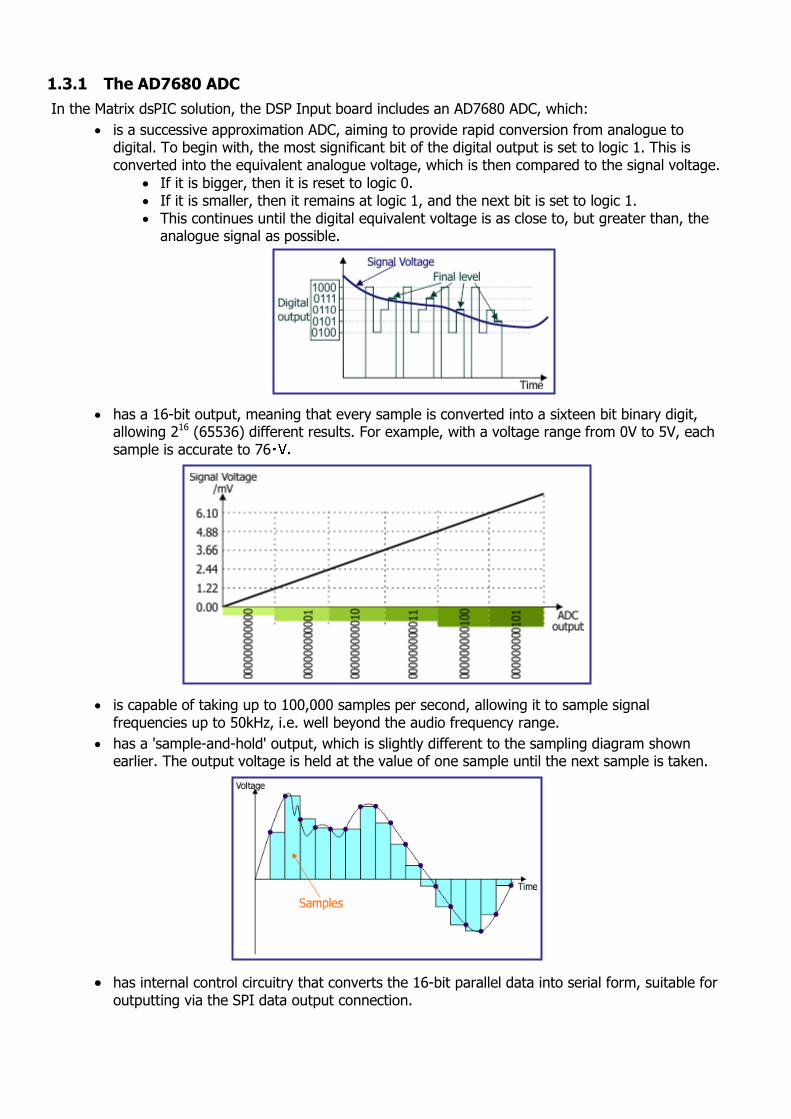
In the Matrix dsPIC solution, the DSP Input board includes an AD7680 ADC, which:
is a successive approximation ADC, aiming to provide rapid conversion from analogue to digital. To begin with, the most significant bit of the digital output is set to logic 1. This is converted into the equivalent analogue voltage, which is then compared to the signal voltage.
If it is bigger, then it is reset to logic 0. If it is smaller, then it remains at logic 1, and the next bit is set to logic 1. This continues until the digital equivalent voltage is as close to, but greater than, the
analogue signal as possible.
has a 16-bit output, meaning that every sample is converted into a sixteen bit binary digit, allowing 216 (65536) different results. For example, with a voltage range from 0V to 5V, each sample is accurate to 76
is capable of taking up to 100,000 samples per second, allowing it to sample signal frequencies up to 50kHz, i.e. well beyond the audio frequency range.
has a 'sample-and-hold' output, which is slightly different to the sampling diagram shown earlier. The output voltage is held at the value of one sample until the next sample is taken.
has internal control circuitry that converts the 16-bit parallel data into serial form, suitable for outputting via the SPI data output connection.
1.4 Digital to Analogue Conversion:
Once the microcontroller has performed its digital processing on the signal, it may be necessary to convert it back to analogue form. This is done by a digital-to-analogue converter (DAC).
It aims to produce an analogue voltage which reflects the size of the input digital signal. The following table illustrates this idea:
Important characteristics for these devices include:
Resolution: the number of possible output voltage levels that it can produce. For example, a 8-bit DAC has 256 (=28) output voltage levels.
Maximum sampling rate: depends on the maximum speed at which the circuit can operate stably. When used in conjunction with an ADC, this can determine the signal frequency range which the system can handle effectively.
Monotonicity: means that the output voltage always increases when the input digital signal increases.
Dynamic range: the difference between the largest and smallest signals that can be used with the DAC.
Digital input Analogue output
0000 0V
0001 0.1V
0010 0.2V
0011 0.3V
0100 0.4V
0101 0.5V
0110 0.6V
0111 0.7V

1.4.1 The AD5662 DAC
In the Matrix dsPIC solution, the DAC function is carried out by a AD5662 chip, found on the 'DSP Output' board, (EB086).
The AD5662 :
is a 'string' DAC. The following circuit diagram shows the principle for a 2-bit DAC.
The string of four resistors (for a 2-bit DAC,) divides the voltage VS into four equal chunks. The 2-to-4 decoder uses the digital input to activate one of the outputs labelled W to Z. This in turn operates one of the four electronic switches. As a result, the analogue output voltage is selected by the digital input to be 0V, VS/4, VS/2 or 3VS/4.
is a 16-bit DAC, meaning that it can cope with digital inputs up to sixteen bits long (giving it 216 = 65,536 different values) . The output analogue voltage has a range from 0V to the positive supply voltage used, VS. Put simply, if used with a reference voltage of 5V, the analogue output will increase i V, as the digital input number increases.
has a settling time of 10ms, meaning that it takes only 10 milliseconds (0.01s) to adjust the analogue output voltage after the input digital signal changes.

2 Program 1 - Laying the foundations
2.1 Introduction
This exercise looks at the basis of all digital audio technology - inputting an audio signal into the microcontroller system, and creating an audio output after the digital processing.
2.2 Objective
To input a signal from a microphone into the microcontroller system, and output an identical sound generated to a loudspeaker or earpiece.
2.3 Requirements
This exercise requires:
a dsPIC EB091 programmer
a copy of Flowcode 6 (or later) running on the PC
a DSP Input E-Block (EB085)
a DSP Output E-Block (EB086)
a graphical LCD E-Block (EB084)
a universal power supply
a high impedance microphone and earpiece.
2.4 Flowcode program outline
The aim of the program is to:
initialise:
the DSP system;
the graphical LCD;
the SPI (Serial Peripheral Interface) component.
sample the audio input;
convert it to a digital signal, using the ADC;
process it with the dsPIC (i.e. transfer it to the output buffer and hence via the DAC to the speaker on the DSP output board, or to the earpiece;
display the name of the program "1. DSP Through" on the gLCD.
2.5 The system components
The flowchart controls five components:
the DSP System component, called 'DSPSystem1';
the Input component, called 'DSPInput1';
the Output component, called 'DSPOutput1';
the SPI component;
the graphical LCD component.

2.5.1 The DSP System component
The DSP System component manages the buffers used by the system.
Each link between components needs a buffer, a number store, to hold data, transmitted from one component to the next. The data is stored in the buffer as a series of binary numbers, here either 8-bits or 16-bits in length. (The buffer depth can be set when the DSP System component is configured.) The location of the data waiting to be processed next is indicated by the 'buffer pointer'.
Each time that the on-board timer 'overflows' (reaches its maximum count,) it sends out a 'tick', (brief trigger pulse), which can be used to increment the buffer pointer, to move from one stored value to the next. The size of each buffer dictates the number of 'ticks' needed to reach the end of that buffer. Knowing the 'tick' rate and the size of the buffer allows us to calculate the delay caused in reading the complete buffer.
2.5.2 The DSP Input component
The DSP Input component controls the buffer called 'AudioSignal'. Each sample from the ADC is stored in this buffer ready for processing by the dsPIC program.
2.5.3 The DSP Output component
After processing, the result is stored in the buffer controlled by the DSP Output component, and can be transferred from there to the DSP Output E-Block.
2.5.4 The SPI component
The SPI component controls the 'conversations' between the SPI master (the microcontroller) and the SPI slave peripherals (here, the DSP Input and DSP Output E-block boards).
It specifies:
the connections to the microcontroller;
the frequency and other clock properties;
whether SPI communication is carried out using hardware or software.
The software option means that the communication is controlled by part of the program. This may be desirable when additional communication channels are needed, or the SPI hardware pin is in use for a different purpose.
Both slave devices use the three wire version of SPI, as they only either read or write. The master uses the four wire version to allow it to select which of these to talk to. The 'Data Out' pin doesn’t go to the ADC and the 'Data In' pin doesn’t go to the DAC!
2.5.5 The graphical LCD component
The graphical LCD component controls the properties of the attached LCD E-Blocks board (EB084). These include:
the connections to the microcontroller;
the display properties - colours used for foreground and background, colour intensity etc.
2.6 Creating the program
Write the Flowcode program using the following steps as a guide:
create a new Flowcode flowchart;
select the EB091 (from PIC16 pack) as a target;
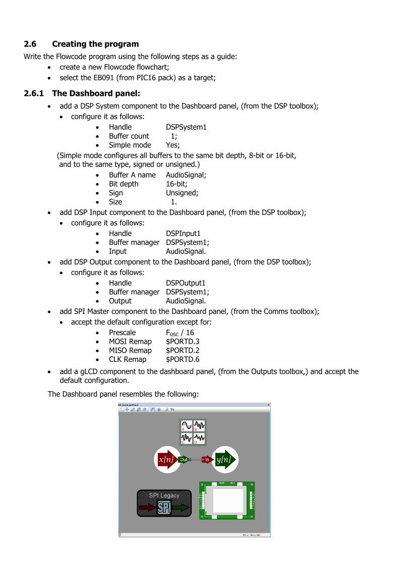
2.6.1 The Dashboard panel:
add a DSP System component to the Dashboard panel, (from the DSP toolbox);
configure it as follows:
Handle DSPSystem1
Buffer count 1; Simple mode Yes;
(Simple mode configures all buffers to the same bit depth, 8-bit or 16-bit, and to the same type, signed or unsigned.)
Buffer A name AudioSignal; Bit depth 16-bit; Sign Unsigned;
Size 1.
add DSP Input component to the Dashboard panel, (from the DSP toolbox);
configure it as follows:
Handle DSPInput1 Buffer manager DSPSystem1; Input AudioSignal.
add DSP Output component to the Dashboard panel, (from the DSP toolbox);
configure it as follows:
Handle DSPOutput1 Buffer manager DSPSystem1; Output AudioSignal.
add SPI Master component to the Dashboard panel, (from the Comms toolbox);
accept the default configuration except for:
Prescale FOSC / 16 MOSI Remap $PORTD.3 MISO Remap $PORTD.2 CLK Remap $PORTD.6
add a gLCD component to the dashboard panel, (from the Outputs toolbox,) and accept the default configuration.
The Dashboard panel resembles the following:

2.6.2 The flowchart:
Create the Flowcode flowchart shown in the following diagrams.
It consists of a 'Main' flowchart, and five macros.
Save the program as 'Exercise 1'.
It will not simulate easily, as it requires samples from the ADC on the DSP Input board.
Main GLCD_Init timer_tick
SPI_Init Read_ADC Write_DAC

2.6.3 The hardware:
Check that the dsPIC programmer is EB091
Configure the jumpers as follows:
Voltage source selector - position PSU;
PICkit / ICSP selection jumper - USB position;
Connect the gLCD E-Blocks board, EB084, to Port B 0-7. Provide power for the board by connecting the '+V' screw terminal to the '+V' screw terminal on the programmer EB091.
Configure the jumpers as follows:
+V voltage selection jumper - 3V3;
Patch system - default position.
Connect the DSP Input E-Blocks board, EB085, to one of the connectors on the dual E-Blocks IDC cables, plugged into Port D 0-7. Provide power by connecting the '+V' screw terminal to the '+V' screw terminal on the programmer EB091.
Configure the jumpers as follows:
Patch system jumper - patch position;
Low-pass filter selection jumper - 3.4kHz
Line in voltage bias jumper - on
Microphone / jack input selection jumper - jack.
Connect the DSP Output E-Blocks board, EB086, to the other connector on the dual E-Blocks IDC cables, plugged into Port D 0-7. Provide power by connecting the '+V' screw terminal to the '+V' screw terminal on the programmer EB091.
Configure the jumpers as follows:
Patch system jumper - patch position;
Low-pass filter selection jumper - 3.4kHz;
Speaker / Line out selection jumper - 'Line out' for earpiece, or 'Speaker' for on-board loudspeaker;
PWM / DAC input selection jumper - DAC.
Connect the EB091 programmer to the PC with a USB cable inserted in the “GHOST” USB socket.
Connect the universal power supply, HP2666, to the EB091 programmer - the green 'Power' LED will light.
Next, compile the program 'Exercise 1' and transfer it to the dsPIC chip.
2.6.4 Testing:
Plug a high impedance microphone into the 'Line in' input jack socket on the DSP Input board.
Plug an earphone into the 'DSP Output' jack socket on the DSP Output board.
Any sounds picked up by the microphone should be relayed to the earphone.
Disconnect the USB lead from the computer to confirm that the program is contained in, and running from the dsPIC.

2.6.5 The Flowcode program in detail
The task of the dsPIC microcontroller is straightforward. It transfers the digital signal received from the ADC to the DAC on the DSP Output board.
The next section goes into detail about the function of each section of the program.
Main:
macro 'GLCD_Init' is called to initialise the gLCD component;
macro 'SPI_Init', is called to initialise the SPI component;
a component macro is used to initialise the DSP component;
an interrupt is set up so that when Timer 1 overflows (reaches its maximum count,) it calls the 'timer_tick' macro;
an empty infinite loop keeps the program active, without doing anything, so that these Timer 1 interrupts keep occurring.
GLCD_Init - sets up the graphical LCD to display the message "1. DSP Through":
component macro 'Initialise' is called to initialise the gLCD component;
component macro 'SetDisplayOrientation' sets the display orientation on the LCD screen;
the 'Print' component macro is called to set the display properties, and create the message to be displayed on the LCD.
timer_tick - is triggered when Timer 1 overflows, and creates a new 'tick' to move the process onto the next sample from the ADC:
macro 'Read_ADC' is called to transfer the latest sample to the variable 'Data';
component macro 'AddRawTick' adds this sample to the DSP Input buffer;
the result of the processing, now stored in the DSP output buffer, is transferred to the 'Data' variable by the component macro 'ReadRawTick';
the 'Write_DAC' macro is called to transfer this value to the DAC;
the 'TickAllBuffers' component macro now moves onto the next sample taken from the ADC.
SPI_Init - enables the SPI hardware peripheral to control data transfer between the ADC, microcontroller and DAC:
the two Output icons disable the two SPI slave devices, the DSP Input and DSP Output boards, by sending logic 1 to their Slave Select pins, D0 and D1 ;
component macro 'Initialise' then activates the SPI hardware peripheral in readiness for transferring data.
Read_ADC - transfers the next ADC sample to the microcontroller:
the Output icon activates the ADC by sending logic 0 to its Slave Select pin, D0;
three 'GetChar' component macros then transfer data from the ADC, via the SPI bus, to local variables '.upper', '.mid' and '.lower'.
(Using local variables is more memory efficient. Once the macro has finished, the memory used by these local variables is released for use elsewhere. Global variables, on the other hand, occupy memory permanently while the program is running, and so should be used sparingly.)
the Output icon then disables the ADC by sending logic 1 to its Slave Select pin, D0;
SPI data is always 8-bits long, whereas the sample coming from the ADC (and later sent to the DAC) is sixteen bits long. The Calculation icon takes three 8-bit samples from the SPI bus and converts it into standard signed 16-bit format. The 'spare' byte provides extra clock signals required by the slave devices.

The following diagram illustrates the steps involved in this calculation. It assumes typical
initial values for the local variables, '.upper', '.mid', '.lower' and '.Return', ('X' = 'don't care').
Write_DAC - transfers the processed sample from the microcontroller to the DAC:
the Calculation icon chops up the '.value' unsigned integer (16-bits long) into two local byte variables, '.upper' and '.lower', ready for transfer via the SPI bus;
the Output icon activates the DAC by sending logic 0 to its Slave Select pin, D1;
the two byte variables are then sent via SPI to the DAC on the DSP Output board;
the Output icon then disables the ADC by sending logic 1 to its Slave Select pin, D0.
2.7 Further work
Adjust the 'Gain' controls on the DSP Input and DSP Output boards. Notice the difference in the sound produced in the earphone.
Test the 'Volume control on the DSP Output board.
Test the effect on the sound heard of changing the low pass filter settings.
Modify the program so that the graphical LCD displays the message "Program 1" in double width and double height characters.

3. Digital Signal Processing
Digital signal processing (DSP) is used for a range of activities, many replacing, and improving on functions that previously used analogue processing.
This processing. usually happens 'in real time', i.e. as the signals occur, with no time to store signals in memory while processing takes place. Sampling audio signals, at a sample rate of 44.1kHz, allows only 22.7 . In this time, the processor must complete the sampling, process the data, and output the result. Latency (delay while processing takes place,) must be kept to an absolute minimum. This places particular demands on the hardware used in this processing - DSP processors are built for speed!
Generally, DSP also delivers more precision. For example, once digitised, a signal can be amplified by a factor of 5 simply by multiplying all its components by 5!
3.1 The dsPIC microcontroller
The dsPIC microcontroller, sometimes called a digital signal controller (DSC), is designed to carry out digital signal processing in portable embedded systems, such as mobile phones. It developed from the 'normal' microcontroller, and retains many of its features. However, its architecture means that it can operate with very little time lag.
3.1.1 What is a microcontroller?
A microprocessor:
is a single-chip integrated circuit;
is designed to perform arithmetic and logic operations on binary data;
is controlled by a program stored in memory.
Its operations are synchronised by a 'clock' (astable circuit), which may be incorporated into the microprocessor integrated circuit, or may be a peripheral subsystem. As technology has advanced, the 'speed' of this clock (astable frequency) has increased, allowing the microprocessor to carry out tasks more quickly.
A typical microprocessor system consists of the microprocessor 'chip', memory 'chips', input / output 'ports', designed to take in digital signals from the outside world, and later output the results of the processing as a digital signal, back to the outside world.
A microcontroller:
aims to be a compact, program-driven, power-efficient device for controlling electrical and electro-mechanical systems, like television remote controls, microwave ovens, robot arms etc.
developed as a compact version of this system, as a microprocessor which has a clock, a limited amount of memory, and input / output ports, all incorporated into a single chip.
does not need vast processing speed, as mechanical devices tend to move in time spans of seconds rather than nanoseconds. (Many programs have to insert delays to calm down the response of the microcontroller.)
does need enhanced input / output capabilities, and the ability to interface and communicate with a wide range of hardware.
3.1.2 Differences between dsPIC and PIC
The distinction between the two has almost gone, and for some processors it is difficult to categorise them in this way. They share many common features.
Microcontrollers are designed to carry out basic mathematical operations on data received from a range of input sensors in order to control a range of output devices. They use the information from sensors, the controlling program and the interrupt subsystem to control output electrical and electro-mechanical devices.
Traditionally, although their computational power was limited (CPUs operated on eight bits of data initially), their strength lay in the wide range of peripheral units available on-chip.
The tasks they are designed for involve moving, sorting and testing data which is stored in memory, and then outputting the result.
Digital signal processors are designed to stream digital signals, keeping latency (delay) to an absolute minimum, and processing the data in a predictable execution time.
To do this, at the high speed required, they often rely on features like pipelined architecture:
Pipelining allows sections of the processor to execute different parts of the instruction at the same time. As a result, more instructions can be executed in a given time.
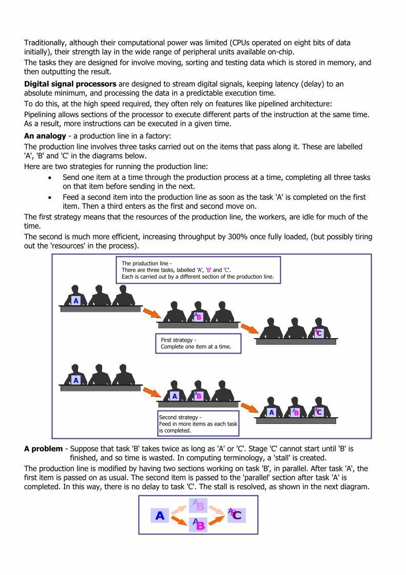
An analogy - a production line in a factory:
The production line involves three tasks carried out on the items that pass along it. These are labelled 'A', 'B' and 'C' in the diagrams below.
Here are two strategies for running the production line:
Send one item at a time through the production process at a time, completing all three tasks on that item before sending in the next.
Feed a second item into the production line as soon as the task 'A' is completed on the first item. Then a third enters as the first and second move on.
The first strategy means that the resources of the production line, the workers, are idle for much of the time.
The second is much more efficient, increasing throughput by 300% once fully loaded, (but possibly tiring out the 'resources' in the process).
A problem - Suppose that task 'B' takes twice as long as 'A' or 'C'. Stage 'C' cannot start until 'B' is finished, and so time is wasted. In computing terminology, a 'stall' is created.
The production line is modified by having two sections working on task 'B', in parallel. After task 'A', the first item is passed on as usual. The second item is passed to the 'parallel' section after task 'A' is completed. In this way, there is no delay to task 'C'. The stall is resolved, as shown in the next diagram.
Second strategy - Feed in more items as each task is completed.
First strategy - Complete one item at a time.
The production line - There are three tasks, labelled 'A', 'B' and 'C'. Each is carried out by a different section of the production line.

3.1.3 Dynamic pipelining
Dynamic pipelines have the flexibility to schedule processing in a way that copes with stalls.
In general, executing instructions involves the following five steps:
fetching the instruction from memory;
decoding the instruction;
accessing any data needed from memory;
processing the instruction;
storing the result in a register.
A dynamic pipeline is divided into three sections:
the instruction 'fetch and decode' unit;
a number of 'functional' units, each of which has a 'reservation station', in effect a buffer, to store the instruction and data;
a commit unit, which writes the result to a specified register at the appropriate time.
Of these, the instruction fetch/decode unit task happens first. Similarly, the commit unit task executes last. The functional units operate in any order within this plan. If a stall occurs, the processor can schedule other instructions to be executed until the stall is resolved.
3.1.4 Other DSP features
hardware multipliers:
Doing it in software would be too slow! Most modern processors now operate with 16-bit precision, (i.e. process 16-bit numbers). When multiplying one 16-bit number by another, the result can have 32 bits. The processor must be able to store these huge numbers.
accumulators:
are used to store these long numbers produced by multiplication. Typically, in a 16-bit system, the accumulator will store up to 40-bit numbers, allowing a number of 'guard bits' for use in further operations like addition. Usually, it uses saturation logic.
MAC hardware:
In many DSP operations, the result is found by repeated 'multiply then add' stages. In a digital filter, for example, the output is found by a calculation of the form:
meaning that the value of 'y' is found by multiplying the current value of 'x' by 'a', and then adding it (the ' x x'.

This process is represented in the following diagram:
This could be done slowly in software, or extremely quickly using a MAC (Multiply - ACcumulate unit) in hardware.
dual data fetch:
The processor must fetch two data items ('a' and 'x' in the example above,) before it can carry out the MAC instruction. This is made easier if the data memory is divided into two discrete areas, one for each of the data items. The architecture of the CPU allows it to access both items within the same clock pulse, speeding up the process.
saturation logic:
For a given data bus or register width, there is a maximum number that can be stored, (when all bits are set to logic 1). In normal processing, 'wrap-around' takes place, when that maximum value is exceeded, and this usually results in a totally incorrect value.
For example, if only four bits can be stored by the CPU, then adding 1 (00012) to 15 (11112) causes an error.
The answer appears to be '0000' as the carry forward is lost. In other words, adding '12' to the maximum value (11112) generates the minimum value (00002).
With saturation logic, when the result of an operation, such as addition or multiplication, is greater than the maximum number possible, it is set ("clamped") to the maximum. Similarly, if it is below the minimum possible, it is clamped to the minimum. In the example above, it clamps the value at '11112'.
barrel shifters:
It is usually necessary to scale ('normalise') data entering or leaving the MAC unit.
When a binary number is shifted one place to the left in a register, it is effectively multiplied by two. Shifting it one place to the right divides it by two. This operation can be carried out in conventional microcontrollers, but only one place left or right at a time.
To shift a number 'n' places would require 'n' clock cycles, and hence be a slow process. A barrel shifter can shift data by a specified number of bits in a single clock cycle.
circular buffers:
A circular buffer is an area of memory used to store incoming data, such as the latest sample from the ADC. The size of the buffer is fixed and it uses the FIFO (first-in-first-out) principle once the buffer is full - as new data arrives, the oldest data is over-written. It is designed to perform as quickly as possible, using as few clock cycles as possible, in other words.

In a conventional (linear) buffer, when more data is added, the existing data is shuffled along.
Picture a line of people on chairs in the doctor's waiting room - as the one at the front of the queue moves off to see the doctor, everyone else moves onto the next chair, and a new arrival can sit on the end chair. Shifting data, in this way, from one location to the next in a linear buffer, takes a lot of clock cycles (time).
A circular buffer is not circular - it just behaves as if it were! Once data is added to the end location in the buffer, the next data is added to the beginning, as the diagram shows. Circular buffers operate by 'moving' a pointer through the data, not moving the data itself.
They are controlled by four 'pointers' - memory locations that contain important addresses. These store the addresses of:
the first memory location in the buffer;
the last memory location in the buffer;
the 'step size' - added to a given buffer address to find the next address in the circular buffer;
the latest addition to the buffer.
When new data is added or removed, the previous data is not shuffled into new locations in memory. Instead only the contents of the 'latest' pointer are changed. The other pointers are unaffected. All this can be accomplished with very little latency.
The 'step size', also called 'stride', is not necessarily '1'. The buffer does not have to occupy adjacent memory locations, but can be spread across an area of memory. If the data has more bits than a single memory location can store, it is stored in more than one memory location. This will be reflected in the contents of the 'step size' pointer. For example, if the data requires two memory locations to store it, then the 'step size' will be two, in order to take the processor to the next item of data.

modulo addressing
When data is ready to be stored in a circular buffer, the 'latest' pointer is used to identify the correct address location for it. Once that is stored, the address in that pointer is changed, guided by the 'step size' pointer.
The system must perform 'boundary checks' to ensure that the address pointed to lies within the circular buffer. This could be done by a software routine, but that would require clock cycles, and hence take time. Instead, the changes to the 'latest' pointer and the checks are done in hardware, using a subsystem called the Address Generator Unit (AGU) with no 'cost' in execution time.
When the address generated lies above the highest location in the circular buffer, the hardware produces an effective address at the lowest address in the buffer. Equally, where the address generated lies below the lowest address used, it is redirected to the highest address in the buffer. This is called 'modulo addressing'.
bit-reversed addressing
Another addressing mode generated by the AGU, bit-reversed addressing does exactly that - the least-significant bit of the number becomes the most-significant bit, and so on. This is illustrated in the following table.
Memory location address -
linear
Memory location address -
bit-reversed
Decimal Binary Binary Decimal
0 0000 0000 0
1 0001 1000 8
2 0010 0100 4
3 0011 1100 12
4 0100 0010 2
5 0101 1010 10
6 0110 0110 6
7 0111 1110 14
8 1000 0001 1
9 1001 1001 9
10 1010 0101 5
11 1011 1101 13
12 1100 0011 3
13 1101 1011 11
14 1110 0111 7
15 1111 1111 15
This can be used to manage the addresses inside a circular buffer.

It is also used within Fourier transformations, which allow signals to be viewed as both time-varying and frequency-varying quantities (i.e. in voltage/time graphs and voltage/frequency graphs.)
As part of the Fourier transformation, a signal with, for example sixteen samples, is 'decomposed' into sixteen signals, each having one sample. This process is illustrated in the next diagram.
The samples are stored in sequence in memory, and then a bit-reversal algorithm is used to access them in the required order. (Compare the numbers of the samples with the final column in the previous table.)
direct memory access (DMA)
Another time-saving measure, direct memory access allows hardware subsystems to access the system memory independently of the main processor.
Input/output operations can take up a lot of time. Instead of carrying out such tasks itself, the CPU can control a separate DMA controller to accomplish data transfer. While this is taking place, the CPU is free to perform other tasks.
4 Program 2 - Adding an echo
4.1 Introduction
The example demonstrates a simple DSP audio through system where data is taken in using the input E-block and output using the output E-block. A delayed version of the input is added to the input and applied to the output to create an echo effect.
4.2 Objective
To input a signal from a microphone into the microcontroller system, and generate an identical sound, with added echo, from its output.
4.3 Requirements
This exercise requires: a dsPIC EB091 programmer
a copy of Flowcode 6 (or later) running on the PC
a DSP Input E-Block (EB085)
a DSP Output E-Block (EB086)
a graphical LCD E-Block (EB084)
a high impedance microphone and earpiece
a universal power supply.
4.4 Flowcode program outline
The aim of the program is to:
initialise:
the DSP system;
the graphical LCD;
the SPI component.
sample the audio input;
convert it to a digital signal, using the ADC;
process it with the dsPIC
scale it, to avoid 'overflows' during summation;
sum it with a delayed version of itself;
transfer the result to the output buffer.
transfer the result to the DAC, and then pass the audio signal produced to the speaker on the DSP output board;
display the name of the program "2. DSP Echo" on the gLCD.

4.5 The system components
The flowchart controls eight components:
the DSP System component, called 'DSPSystem1';
the Input component, called 'DSPInput1';
the Output component, called 'DSPOutput1';
the Scale component, called 'DSPScale1';
the Sum component, called 'DSPSum1';
the Delay component, called 'DSPDelay1';
the SPI component;
the graphical LCD component.
Five of these were described in Program 1. The new ones are described below.
4.5.1 The DSP Scale component
The DSP Scale component allows the program to change the number stored in a buffer, by either adding or subtracting a value to it, or by dividing or multiplying it by a number.
The simplest way to multiply or divide is to shift the number to the left (multiply) or the right (divide). Shifting by one place causes multiplication/division by two, two places by four, three by eight etc.
The diagram below illustrates the effect of shifting the binary number 0001 0110 to the left and to the right by one place.
In this program, it is used with the 'RightShiftTick' macro, given a parameter of '1', to divide the latest sample in the 'AudioSignal' buffer by two, and store the result in the 'AudioScaled' buffer.
4.5.2 The DSP Sum component
The DSP Sum component combines together the contents of two buffers into one buffer. There are a variety of options for how this is done. The combination can be the sum, the average, the difference, the greater of, or smaller of the individual buffers, for example.
In this case, it uses the 'AddTick' macro to sum the contents of the 'AudioScaled' and 'AudioDelayed' buffers, storing the result in the 'AudioDelayed' buffer.
4.5.3 The DSP Delay component
The DSP Delay component allows a delay to be inserted before a signal takes effect. The delay involves moving the sample to a later position. The delay is measured as the number of samples involved in this change of position.
4.6 Creating the program
Write the Flowcode program using the following steps as a guide:
create a new Flowcode flowchart;
select the EB091 (PIC16 pack) as a target;
4.6.1 The Dashboard panel:
add a DSP System component to the Dashboard panel, (from the DSP toolbox);
configure it as follows:
Handle DSPSystem1; Buffer count 4;
Simple mode Yes; Buffer A name AudioSignal; Buffer B name AudioScaled; Buffer C name AudioDelayed; Buffer D name AudioSum; Bit depth 16-bit; Sign Unsigned; Size 1.
add DSP Input component to the Dashboard panel, (from the DSP toolbox);
configure it as follows:
Handle DSPInput1; Buffer manager DSPSystem1; Input AudioSignal.
add DSP Output component to the Dashboard panel, (from the DSP toolbox);
configure it as follows:
Handle DSPOutput1; Buffer manager DSPSystem1; Output AudioSum.
add DSP Scale component to the Dashboard panel, (from the DSP toolbox);
configure it as follows:
Handle DSPScale1; Buffer manager DSPSystem1; Input AudioSignal; Output AudioScaled.
add DSP Sum component to the Dashboard panel, (from the DSP toolbox);
configure it as follows:
Handle DSPSum1; Buffer manager DSPSystem1; Input A AudioScaled; Input B AudioDelayed; Output AudioSum.

add DSP Delay component to the Dashboard panel, (from the DSP toolbox);
configure it as follows:
Handle DSPDelay1; Max Delay Count 750; Initial Delay Count 750 Buffer manager DSPSystem1; Input AudioScaled; Output AudioDelayed; Sample rate 8000.000000.
add SPI Master component to the Dashboard panel, (from the Comms toolbox);
accept the default configuration except for:
Prescale FOSC / 16 MOSI Remap $PORTD.3 MISO Remap $PORTD.2 CLK Remap $PORTD.6
add a gLCD component to the dashboard panel, (from the Outputs toolbox,) and accept the default configuration.
The Dashboard panel resembles the following:

4.6.2 The flowchart:
Create the Flowcode flowchart shown in the following diagrams.
It consists of a 'Main' flowchart, and five macros.
Four of these macros, 'Main', 'SPI_Init', 'Read_ADC' and 'Write_ADC' are identical to those in program 1, and may be imported from there.
The 'GLCD_Init' macro has only a minor change from that used in program 1 - the text printed on the gLCD is different.
The 'timer_tick' macro has additional component macros, to take care of the scaling, echo production and summation.
Main GLCD_Init timer_tick
SPI_Init Read_ADC Write_DAC

Save the program as 'Exercise 2'.
Once again, it will not simulate easily, as it requires samples from the ADC on the DSP Input board.
4.6.3 The hardware:
Check that the dsPIC EB091 programmer jumper settings are the same as in program 1.
Connect the gLCD E-Blocks board, EB084, to Port B 0-7. Provide power for the board by connecting the '+V' screw terminal to the '+V' screw terminal on the EB091 programmer.
The jumper settings are the same as in program 1.
Connect the DSP Input E-Blocks board, EB085, to one of the connectors on the dual E-Blocks IDC cables, plugged into Port D 0-7. Provide power by connecting the '+V' screw terminal to the '+V' screw terminal on the EB091 programmer.
The jumper settings are the same as in program 1.
Connect the DSP Output E-Blocks board, EB086, to the other connector on the dual E-Blocks IDC cables, plugged into Port D 0-7. Provide power by connecting the '+V' screw terminal to the '+V' screw terminal on the EB091 programmer.
The jumper settings are the same as in program 1.
Connect the EB091 programmer to the PC with a USB cable inserted in the “GHOST” USB socket.
Connect the universal power supply, HP2666, to the EB091 programmer - the green 'Power' LED will light.
Next, compile the program 'Exercise 2' and transfer it to the dsPIC chip.
4.6.4 Testing:
Plug a high impedance microphone into the 'Line in' input jack socket on the DSP Input board.
Plug an earphone into the 'DSP Output' jack socket on the DSP Output board.
Any sounds picked up by the microphone should be relayed to the earphone, but this time with an added echo.
The echo effect will be more apparent if you make short 'clicking' sounds into the microphone.

4.6.5 The Flowcode program in detail
The task is:
to take in a sample from the ADC on the DSP Input board;
divide it by two, to prevent excessive values when the summation takes place;
produce a delayed version of it;
add together the original (scaled) sample and its delayed equivalent;
output the result from the dsPIC to the DAC on the DSP Output board;
send the DAC output to the speaker on the DSP Output board.
The next section goes into detail about the function of each section of the program, though much of this is the same as in program 1.
Main macro:
has the same function as in program 1.
GLCD_Init:
sets up the graphical LCD to display the message "2. DSP Echo":
timer_tick:
is triggered when Timer 1 overflows, and creates a new 'tick' to move the process onto the next sample from the ADC:
macro 'Read_ADC' is called to transfer the latest sample to the variable 'Data';
component macro 'AddRawTick' adds this sample to the DSP Input buffer, without scaling it in any way;
component macro 'RightShiftTick' moves all bits of the sample one place to the right in the buffer, effectively dividing the value by two;
component macro 'DelayTick' takes a copy of this sample, and adds a time delay, measured as the number of samples by which it is delayed;
component macro 'AddTick' sums together the original sample and its delayed version;
the result of the processing, stored in the DSP output buffer, is transferred to the 'Data' variable by the component macro 'ReadRawTick';
the 'Write_DAC' macro is called to transfer this value to the DAC;
the 'TickAllBuffers' component macro now moves onto the next sample taken from the ADC.
SPI_Init: enables SPI peripheral to control data transfer between the ADC, microcontroller and DAC, as
in program 1.
Read_ADC:
configures and transfers the next ADC sample to the microcontroller, as in program 1.
Write_DAC:
transfers the processed sample from the microcontroller to the DAC, as in program 1.
4.7 Further work
Familiarise yourself with the controls on the DSP Input and DSP Output boards again:
Adjust the 'Gain' controls. Notice the effect on the sound produced.
Test the 'Volume control on the DSP Output board.
Changing the low pass filter settings, and observe the effect on the sound heard.
Change the delay settings - 'Max Delay Count' and 'Initial Delay Count', on the DSP Delay component and notice the effect on the sound heard.
Observe the effect of changing the 'Scaler' parameter in the 'RightShiftTick' macro.
5. DSP Communications
5.1 Communication options
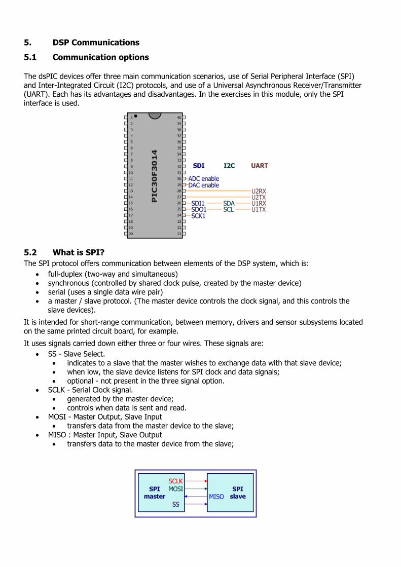
The dsPIC devices offer three main communication scenarios, use of Serial Peripheral Interface (SPI) and Inter-Integrated Circuit (I2C) protocols, and use of a Universal Asynchronous Receiver/Transmitter (UART). Each has its advantages and disadvantages. In the exercises in this module, only the SPI interface is used.
5.2 What is SPI?
The SPI protocol offers communication between elements of the DSP system, which is:
full-duplex (two-way and simultaneous) synchronous (controlled by shared clock pulse, created by the master device) serial (uses a single data wire pair) a master / slave protocol. (The master device controls the clock signal, and this controls the
slave devices).
It is intended for short-range communication, between memory, drivers and sensor subsystems located on the same printed circuit board, for example.
It uses signals carried down either three or four wires. These signals are:
SS - Slave Select. indicates to a slave that the master wishes to exchange data with that slave device; when low, the slave device listens for SPI clock and data signals; optional - not present in the three signal option.
SCLK - Serial Clock signal. generated by the master device; controls when data is sent and read.
MOSI - Master Output, Slave Input transfers data from the master device to the slave;
MISO : Master Input, Slave Output transfers data to the master device from the slave;

SPI is a protocol concerned with data exchange, controlled by the clock line, SCLK, which, in turn, is under the control of the master device. Data is synchronised with the clock signal, so that typically, it changes only during the falling edges of the clock pulse. It is read only on the rising edges.
To begin data transfer, the master creates a clock signal at a frequency that the slave device can handle. It then chooses the slave device using the Slave Select line. Since SPI transmits its clock signal between devices, to synchronise the data exchange, the clock frequency can vary without disrupting the data transfer. The data rate simply changes along with the changes in the clock rate. With asynchronous communication protocols, like RS232, this is not possible.
In SPI, no device is just a 'transmitter' or just a 'receiver'. Each device has two data lines, one to input data and one to output it. During each clock cycle, full-duplex communication takes place, i.e. the master sends the slave one bit (usually the most-significant bit of the eight-bit data frame) on the MOSI line, and receives one bit from the slave, on the MISO line. A program should always read incoming data after a transfer has taken place, even if it is not used in the program, otherwise the SPI module may become disabled. To terminate the transmission, the master stops sending further clock pulses.
5.2.1 Three Wire SPI:
Three wire SPI is used:
within the ADC on the DSP Input board, where the master receives data from the slave device, but does not send data back to it;
within the DAC on the DSP Output board, where the master sends data to the slave device, but does not read data back from it.
No Slave Select pin is needed in the exercises as the dsPIC uses Port D bit 1 and bit 0 to activate the DAC and ADC respectively.
5.2.2 Four Wire SPI:
Four wire SPI allows the master to select the slave device, and then enables the master to both send data to the slave device and receive data back from it. A single SPI operation simultaneously transfers a byte of data from the master to the slave via the MOSI signal and also a byte of data from the slave to the master via the MISO signal.

5.3 What is I2C?
The I2C (Inter Integrated Circuit) protocol is also intended for short-range communication. It is:
half-duplex (two-way but only one at a time)
synchronous (controlled by shared clock pulse, created by the master device)
serial (uses a single data wire pair)
multi-master (rarely) / multi-slave protocol. (Master devices initiate all communication with the slave devices).
It uses two wires to connect all devices, sending signals known as SCL, the clock signal, and SDA, the data signal. Data is transferred in eight-bit frames. Both wires are normally held at logic 1 by pull-up resistors. Any device pulling the wire low causes all devices to see a low logic value. Clock signals are used to synchronise communication between the master device and the chosen slave, and can be up to 100kHz, in standard mode I2C.
Devices are either masters or slaves. Masters initiate and control communication with slaves, using 'Start' and 'Stop' signals. Slaves respond.
The start and stop bits mark the beginning and end of a conversation with the slave device. The Start and Stop bits are identified as such because these are the only places where the SDA (data line) changes while the SCL (clock line) is high. A high-to-low transition on SDA is used as a Start bit, and a low-to-high transition for a Stop bit.
To begin a transmission, the master device sends a Start bit, followed by the address of the slave device. The address is usually seven bits long, but may be ten bits. After the seven address bits, the master adds an eighth data-direction bit, to complete the frame. This tells the slave whether to listen to the transmission, (logic 0), or send data to the master, (logic 1).
When data is being transferred, SDA must remain at either logic 0 or logic 1 whilst SCL is high. Data is changed, when necessary, on the falling-edge of the clock pulse, and sampled on the rising-edge of the clock pulse. To transmit data, the most-significant bit (msb) of the eight-bit frame is placed on SDA. The SCL wire is then pulsed high and low. After the frame of eight bits is completed, the receiving device must send an acknowledgement bit, (logic 0), before further data can be sent. At the end of the transmission, the master sends a Stop bit.

5.4 What is UART?
UART stands for Universal Asynchronous Receiver and Transmitter, a common device for transmitting data between subsystems in a computer, or between computers via a modem. It contains a buffer, (shift register), to which data is added by the transmitting processor. It converts this data from parallel to serial format (and back again at the receiver).
5.4.1 What's in a name?
Universal - The UART does not itself determine, nor create, the physical signal that is transmitted between devices. That task is done by the line driver circuitry appropriate to the media being used. It can use a variety of different media and protocols to deliver and collect the data, including copper wire, optical fibre or a wireless link.
Asynchronous - the communicating devices do not share a common clock, unlike the SPI and I2C protocols. Instead, both the transmitting and receiving UART has its own clock, but they use the data exchanged to synchronise them.
At a minimum, they synchronise their clocks on the falling edge of the 'Start' bit, but, in more complex devices, may repeat this synchronisation while the data exchange is taking place. As a result, the transmission takes place down a single wire, not two.
Receiver/Transmitter - UARTs are responsible for both sending and receiving serial data.
To transmit, the UART creates the data packet, generating and adding a parity bit to it if needed. This is outputted in serial format, least-significant bit first, from the 'TX' pin.
To receive, the UART samples the 'RX' pin level. Normally this sits at logic 1. When a transmission is received, the pin drops to logic 0, indicating the Start bit. The received data is then transferred into the 'Receive' buffer, ready for transfer, in parallel format, to the processor.
5.4.2 Typical UART
The following diagram depicts the functionality of a typical UART chip.
The details:
Ck - controls all actions of the UART hardware.
The receiving UART tests the state of the incoming signal on each clock pulse. When it senses a Start bit, the subsequent data bits, usually 8, are clocked into the 'Receive' buffer. On completion, the UART sets a flag to indicate the arrival of new data, and may also generate an interrupt to signal that the processor may copy and process it.
I/O - tells the UART whether to transmit the data from its 'Transmit' buffer, or monitor the 'Rx' pin, looking for an incoming data transfer.
Int - outputs an interrupt to trigger action in the processor.
D7...D0 - data pins to transfer data from the processor to the 'Transmit' buffer, or store incoming data.
Tx - serial transmit pin.
Rx - serial receive pin.
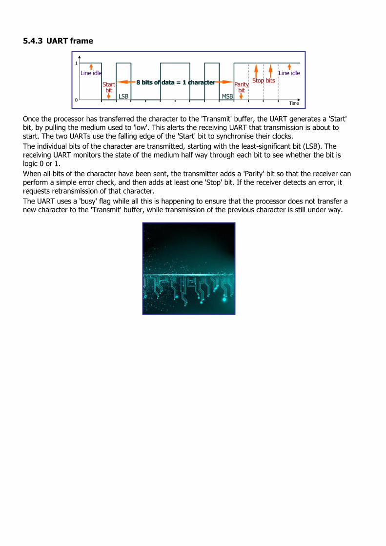
5.4.3 UART frame Once the processor has transferred the character to the 'Transmit' buffer, the UART generates a 'Start' bit, by pulling the medium used to 'low'. This alerts the receiving UART that transmission is about to start. The two UARTs use the falling edge of the 'Start' bit to synchronise their clocks.
The individual bits of the character are transmitted, starting with the least-significant bit (LSB). The receiving UART monitors the state of the medium half way through each bit to see whether the bit is logic 0 or 1.
When all bits of the character have been sent, the transmitter adds a 'Parity' bit so that the receiver can perform a simple error check, and then adds at least one 'Stop' bit. If the receiver detects an error, it requests retransmission of that character.
The UART uses a 'busy' flag while all this is happening to ensure that the processor does not transfer a new character to the 'Transmit' buffer, while transmission of the previous character is still under way.

6 Program 3 - Reverberation
6.1 Introduction
The example demonstrates the common technique of adding reverberation, repeated echoes with very short delays, to a signal. This is often done to increase the realism of the sound produced. Without it, sounds produced from digital sources like computers would sound very unrealistic.
In nature, we hear not only the original sound, but a number of echoes from reflecting surfaces around us. If we are out in the open, where there are few reflectors, there is little reverberation. Conversely, when we hear a sound with very little reverberation, our brains' interpretation is that we are outside.
Timing is important. If the gap between the sound and its echo is long enough, we hear it as just that - a sound followed by its echo. If the time is quite short, our brains merge the sound and echo together to give a feeling of being enclosed.
The longer the time between the echoes and the original signal, the further away our brain pictures the reflector, and so the bigger the enclosure we appear to be in. In this way, a sound engineer can conjure up the impression of being in a large auditorium, such as a cathedral, or in a bathroom or even a wardrobe.
6.2 Objective
To input a signal from a microphone into the microcontroller system, and generate an identical sound, with a number of added echoes, from its output.
6.3 Requirements
This exercise requires:
a dsPIC EB091 programmer
a copy of Flowcode 6 (or later) running on the PC
a DSP Input E-Block (EB085)
a DSP Output E-Block (EB086)
a graphical LCD E-Block (EB084)
a high impedance microphone and earpiece
a universal power supply.
6.4 Flowcode program outline
The aim of the program is to:
initialise:
the DSP system;
the graphical LCD;
the SPI component.
sample the audio input;
convert it to a digital signal, using the ADC;
process it with the dsPIC
scale the incoming sample to avoid 'overflows' during summation;
delay and scale a sample taken from the output;
sum these two samples;
transfer the result to the output buffer.
transfer the result to the DAC, and then pass the audio signal produced to the speaker on the DSP output board;
display the name of the program "3. DSP Reverb" on the gLCD.

6.5 The system components
The flowchart controls nine components:
the DSP System component, called 'DSPSystem1';
the Input component, called 'DSPInput1';
the Output component, called 'DSPOutput1';
the first Scale component, called 'DSPScale1', which scales the input sample;
the second Scale component, called 'DSPScale2', which scales the output sample;
the Delay component, called 'DSPDelay1';
the Sum component, called 'DSPSum1';
the SPI component;
the graphical LCD component. All of these have been used, and described earlier. The notes that follow describe their use in this program.
6.5.1 The first DSP Scale component
It is used with the 'RightShiftTick' macro, given a parameter of '1', to divide the latest sample from the ADC, in the 'AudioSignal' buffer, by two, and store the result in the 'AudioScaled' buffer.
6.5.2 The DSP Sum component
Here, it uses the 'AddTick' macro to sum the contents of the 'AudioScaled' and 'FeedbackDelayed' buffers, storing the result in the 'AudioSum' buffer.
6.5.3 The DSP Delay component
The DSP Delay component adds a time delay to the signal, 'AudioSum', fed back from the output. The bigger this time delay, the larger the apparent size of the enclosure containing the sound source. The output of this component is stored in the 'AudioDelayed' buffer.
6.5.4 The second DSP Scale component
This is also used with the 'RightShiftTick' macro, and a parameter of '1', to divide a sample by two. In this case, the sample is taken from the 'AudioDelayed' buffer, the delayed sample from the output of the DSP Sum component. The result, 'FeedbackDelayed', is fed into one input of the DSP Sum component.

6.6 Creating the program
Write the Flowcode program using the following steps as a guide:
create a new Flowcode flowchart;
select the EB091 (from PIC16 pack) as a target;
6.6.1 The Dashboard panel:
add a DSP System component to the Dashboard panel;
configure it as follows:
Handle DSPSystem1; Buffer count 4;
Simple mode Yes; Buffer A name AudioSignal; Buffer B name AudioScaled; Buffer C name AudioDelayed; Buffer D name AudioSum; Buffer E name FeedbackDelayed; Bit depth 16-bit; Sign Unsigned; Size 1.
add DSP Input component to the Dashboard panel;
configure it as follows:
Handle DSPInput1; Buffer manager DSPSystem1; Input AudioSignal.
add DSP Output component to the Dashboard panel;
configure it as follows:
Handle DSPOutput1; Buffer manager DSPSystem1; Output AudioSum.
add the first DSP Scale component to the Dashboard panel;
configure it as follows:
Handle DSPScale1; Buffer manager DSPSystem1; Input AudioSignal; Output AudioScaled.
add DSP Sum component to the Dashboard panel;
configure it as follows:
Handle DSPSum1; Buffer manager DSPSystem1; Input A AudioScaled; Input B FeedbackDelayed; Output AudioSum.

add DSP Delay component to the Dashboard panel;
configure it as follows:
Handle DSPDelay1;
Max Delay Count 750; Initial Delay Count 750 Buffer manager DSPSystem1; Input AudioSum; Output AudioDelayed; Sample rate 8000.000000.
add the second DSP Scale component to the Dashboard panel;
configure it as follows:
Handle DSPScale2; Buffer manager DSPSystem1; Input AudioDelayed; Output FeedbackDelayed.
add SPI Master component to the Dashboard panel, (from the Comms toolbox);
accept the default configuration except for:
Prescale FOSC / 16 MOSI Remap $PORTD.3 MISO Remap $PORTD.2 CLK Remap $PORTD.6
add a gLCD component to the dashboard panel and accept the default configuration. The Dashboard panel resembles the following:

6.6.2 The flowchart:
Create the Flowcode flowchart shown in the following diagrams.
It consists of a 'Main' flowchart, and five macros.
Four of these macros, 'Main', 'SPI_Init', 'Read_ADC' and 'Write_ADC' are identical to those in earlier programs, and may be imported from there.
The 'GLCD_Init' macro has only a minor change - the text printed on the gLCD is different.
The 'timer_tick' macro has additional component macros, to take care of the scaling, feedback and summation.
Main GLCD_Init timer_tick
SPI_Init Read_ADC Write_DAC

Save the program as 'Exercise 3'.
Once again, it will not simulate easily, as it requires samples from the ADC on the DSP Input board.
6.6.3 The hardware:
The hardware set-up is identical to that used in the previous program:
Check that the dsPIC EB091 programmer jumper settings are the same as in program 1.
Connect the gLCD E-Blocks board, EB084, to Port B 0-7. Provide power for the board by connecting the '+V' screw terminal to the '+V' screw terminal on the EB091 programmer.
The jumper settings are the same as in program 1.
Connect the DSP Input E-Blocks board, EB085, to one of the connectors on the dual E-Blocks IDC cables, plugged into Port D 0-7. Provide power by connecting the '+V' screw terminal to the '+V' screw terminal on the EB091 programmer.
The jumper settings are the same as in program 1.
Connect the DSP Output E-Blocks board, EB086, to the other connector on the dual E-Blocks IDC cables, plugged into Port D 0-7. Provide power by connecting the '+V' screw terminal to the '+V' screw terminal on the EB091 programmer.
The jumper settings are the same as in program 1.
Connect the EB091 programmer to the PC with a USB cable inserted in the “GHOST” USB socket.
Connect the universal power supply, HP2666, to the EB091 programmer - the green 'Power' LED will light.
Next, compile the program 'Exercise 3' and transfer it to the dsPIC chip.
6.6.4 Testing:
Plug a high impedance microphone into the 'Line in' input jack socket on the DSP Input board.
Plug an earphone into the 'DSP Output' jack socket on the DSP Output board.
Any sounds picked up by the microphone should be relayed to the earphone, but this time with reverberation.
The reverberation will be more apparent if you make short 'clicking' sounds into the microphone.
6.6.5 The Flowcode program in detail
The task is:
to take in a sample from the ADC on the DSP Input board;
divide it by two, to prevent excessive values when the summation takes place;
add it to a delayed and scaled sample fed back from the output of the DSP Sum component;
output the result from the dsPIC to the DAC on the DSP Output board;
send the DAC output to the speaker on the DSP Output board.
The next section goes into detail about the function of each section of the program, though much of this is the same as in earlier programs.
Main macro:
has the same function as in previous programs.
GLCD_Init:
sets up the graphical LCD to display the message "3. DSP Reverb":
timer_tick: is triggered when Timer 1 overflows, and creates a new 'tick' to move the process onto the
next sample from the ADC: macro 'Read_ADC' is called to transfer the latest sample to the variable 'Data'; component macro 'AddRawTick' adds this sample to the DSP Input buffer, without scaling it
in any way;
component macro 'RightShiftTick' moves all bits of the sample one place to the right in the buffer, effectively dividing the value by two;
component macro 'AddTick' sums together the original sample and a scaled, delayed sample fed back from the output of the DSP Sum component;
component macro 'DelayTick' takes a sample from the output of the DSP Sum component, and adds a time delay to it;
a second component macro 'RightShiftTick' divides this sample by two; the result of the summation is stored in the DSP output buffer, and then transferred to the
'Data' variable by the component macro 'ReadRawTick';
the 'Write_DAC' macro is called to transfer this value to the DAC; the 'TickAllBuffers' component macro now moves onto the next sample taken from the ADC.
SPI_Init:
enables SPI peripheral to control data transfer between the ADC, microcontroller and DAC, as in earlier programs.
Read_ADC:
configures and transfers the next ADC sample to the microcontroller, as previously.
Write_DAC:
transfers the processed sample from the microcontroller to the DAC, as previously.
6.7 Further work
Change the delay settings - 'Max Delay Count' and 'Initial Delay Count', on the DSP Delay component and notice the effect on the sound heard.
Observe the effect of changing the 'Scaler' parameter in the two 'RightShiftTick' macros.

7. Signals and waveforms
Signals carry information - speech, video or other data.
Usually, they do so as a time-varying voltage. They can be analogue signals, which produce a voltage copy of the information, or digital signals, where the information is in the form of a series of numbers, rather like a train timetable. The diagrams above show both types, in the form of voltage-time graphs, in other word how the signals change over time, (in the 'time domain').
However, they can equally be described in terms of their frequency content, (in the frequency domain). Both kinds of diagram show the same signals, but illustrate different aspects of them.
The diagram above represents the frequency spectrum of a signal - the range and strength of frequencies found in the signal. It aims to illustrate several types of unwanted components in the signal, including pink noise and white noise. It also shows two harmonics of the fundamental signal. These have frequencies which are whole number multiples of the fundamental frequency.

7.1 Noise
In electronics, noise is usually an unwanted extra component, a contamination of a signal, produced by an external source.
'White' noise is named because of a comparison with light. White light contains all colours (frequencies) of light. Similarly, 'white noise' is made up of all frequencies. Other sources of noise have a different frequency spectrum, and, to keep the analogy going, are often named after colours, such as pink, blue and grey. 'White' and 'pink' noise are of significance in this course, as the DSP Frequency Generator component within Flowcode 6 (or later) can generate them.
Both 'white' noise and 'pink' noise contain all the frequencies audible to humans. However, 'white' noise has the same power per unit frequency ('per hertz') across all frequencies, whereas the power per unit frequency in 'pink' noise decreases as the frequency increases.
Because of the way we perceive sounds, we use the word 'octave' to mean the range of frequencies between one frequency and double that frequency. For example, 100Hz and 200Hz are one octave apart. That octave, then covers a range of 100Hz. However, the next octave runs from 200Hz to 400Hz, and so has twice as big a range.
As 'white' noise has the same power delivered by each unit of frequency, the higher octaves deliver more total power than lower octaves. To us, then, 'white' noise appears as a high frequency 'hiss', as power is concentrated into the higher octaves.
'Pink' noise, however, appears to be equally loud at all frequencies, rather like the sound of rain falling on the road, or wind rustling through the trees. As frequency increases, the power per unit frequency falls off in such a way that each octave delivers the same power.
Though noise is usually regarded as a nuisance in electronic systems, 'pink' noise is often used to test audio equipment. It may even help insomniacs by inducing deeper sleep!
7.2 Signal waveforms
Different waveforms are used for different purposes:
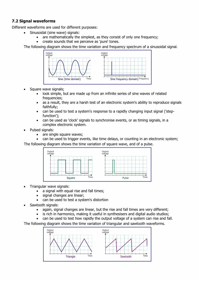
Sinusoidal (sine wave) signals: are mathematically the simplest, as they consist of only one frequency; create sounds that we perceive as 'pure' tones.
The following diagram shows the time variation and frequency spectrum of a sinusoidal signal.
Square wave signals; look simple, but are made up from an infinite series of sine waves of related
frequencies;
as a result, they are a harsh test of an electronic system's ability to reproduce signals faithfully;
can be used to test a system's response to a rapidly changing input signal ('step-function');
can be used as 'clock' signals to synchronise events, or as timing signals, in a complex electronic system.
Pulsed signals: are single square waves; can be used to trigger events, like time delays, or counting in an electronic system;
The following diagram shows the time variation of square wave, and of a pulse.
Triangular wave signals:
a signal with equal rise and fall times; signal changes are linear; can be used to test a system's distortion
Sawtooth signals: again, signal changes are linear, but the rise and fall times are very different; is rich in harmonics, making it useful in synthesisers and digital audio studios; can be used to test how rapidly the output voltage of a system can rise and fall.
The following diagram shows the time variation of triangular and sawtooth waveforms.

8 Program 4 - Sine wave generator
8.1 Introduction
This program demonstrates how to turn the dsPIC microcontroller into a valuable test instrument. It generates sinusoidal signals at a frequency which can be varied using switch settings, and outputs them from the 'Line Output' socket of the DSP Output E-Blocks board. These signals can then be used in measuring the gain of a voltage amplifier, for example, or in determining its bandwidth, (useful frequency range).
8.2 Objective
To generate sine wave signals with a frequency selected using switches.
8.3 Requirements
This exercise requires: a dsPIC EB091 programmer.
a copy of Flowcode 6 (or later) running on the PC
a DSP Output E-Block (EB086)
a graphical LCD E-Block (EB084)
a E-Block Switch board (EB007)
a universal power supply.
8.4 Flowcode program outline
The aim of the program is to:
initialise: the DSP system; the graphical LCD; the SPI component.
sense the state of the switches
generate a digitised sine wave signal from the DSP Frequency Generator component, with a frequency determined by the state of the switches.
process it with the dsPIC scale the ensuing signal data; transfer the result to the output buffer.
transfer the result to the DAC, and then pass the signal produced to the speaker on the DSP output board;
display the name of the program "4. Sine Generator" on the gLCD.
8.5 The system components
The flowchart controls eight components:
the DSP System component, called 'DSPSystem1';
the Frequency Generator component, called 'DSPFreqGen1';
the Scale component, called 'DSPScale1';
the Output component, called 'DSPOutput1';
the SPI component;
the graphical LCD component;
two switches on the E-Blocks Switch Board, called 'sw_slide_sub_pcb1' and 'sw_slide_sub_pcb2'.
Most of these have been described earlier. The notes that follow describe any new components, and distinctive features of others in this program.

0
50
100
150
200
250
1 3 5 7 9 11 13 15 17 19 21 23 25 27 29 31 33 35 37 39 41 43 45 47
Series1
8.5.1 The Frequency Generator component
The Frequency Generator component, used in conjunction with the DSP System component, allows the generation of a range of waveforms, including Sine, Square, Pulse, Triangle and Sawtooth. In addition, there is the ability to generate both Pink and White noise, and to generate a Custom waveform.
Within the Properties for this component:
Waveform type - allows the user to select the waveform 'shape' - sine, square, pulse, triangle, sawtooth, white noise, pink noise, or custom. The choice made affects the appearance of the Frequency Generator symbol on the Dashboard Panel.
Amplitude - the 'height' of the wave, usually measured in volts. Where the signal is used to generate a sound, the amplitude influences the loudness of the sound.
Offset - the 'vertical' starting point for the wave - '127' means starting mid-way up so the wave can grow bigger and smaller by equal amounts.
Period - really, the time taken to produce one cycle of the wave, but in this case that translates to the number of samples in each cycle (as the time to produce one cycle is fixed for the program.
Phase - the equivalent of offset for the 'horizontal' direction, allowing the waveform to have a delayed, or early start.
Data - the values of the samples used to create one cycle of the wave. The values are created automatically by choosing the waveform type. Test this by selecting and deleting the data - it magically re-appears when you hit the 'Return' key. (The only exception is the 'Custom' waveform, where you have to feed in your own data values.)
The diagram that follows shows the data produced by the sine wave generator exported to a spreadsheet, and expressed as a graph.
Period offset - allows the frequency of the wave to be modified. When set to 2, the system reads every other sample, and so completes the cycle in half the time, doubling the frequency. When set to 0.5, each sample is read twice, and so it takes twice as long to create one cycle, halving the frequency.

8.5.2 The DSP Scale component
It is used with the 'LeftShiftTick' macro, given a parameter of '8'. The aim is to convert each 8-bit sample from the Frequency Generator, read from the 'AudioSignal' buffer, into a 16-bit value, which is then stored in the 'AudioScaled' buffer.
This process is illustrated below:
When you simulate this program, select 'View' 'Console'. Compare the data provided under the
'AudioSignal' and 'AudioScaled' tabs to see the results of this process.
8.5.3 The switches
It is used with the 'LeftShiftTick' macro, given a parameter of '8'. The aim is to convert each 8-bit sample from the Frequency Generator, read from the 'AudioSignal' buffer, into a 16-bit value, which is then stored in the 'AudioScaled' buffer.
8.6 Creating the program
Write the Flowcode program using the following steps as a guide:
create a new Flowcode flowchart;
select the EB091 (from PIC16 pack) as a target;
8.6.1 The Dashboard panel:
add a DSP System component to the Dashboard panel;
configure it as follows:
Handle DSPSystem1; Buffer count 2; Simple mode No;
(Setting 'Simple mode' to 'No' means that we can set different bit depths for buffers A and B.)
Buffer A name AudioSignal; Buffer B name AudioScaled;
Buffer A: Bit depth 8-bit; Sign Unsigned; Size 1;
Buffer B:
Bit depth 16-bit; Sign Unsigned; Size 1.

Configuring the 'AudioSignal' buffer with a 8-bit depth' ensures efficient use of ROM memory.
During simulation, the Data Scope automatically scales the trace to take this into account. That is why both the 'AudioSignal' and the 'AudioScaled' traces appear identical. Effectively, they are plotted on different vertical scales.
Typical results are shown in the next diagram:
add DSP Frequency Generator to the Dashboard panel; configure it as follows:
Handle DSPFreqGen1; Buffer manager DSPSystem1; Output AudioSignal; Type Sine; Amplitude 200; Offset 127; Period 50; Phase 0; Data Created automatically as you choose the waveform type;
Period Offset 1.000000 Sample Rate 8000.000000.
Notice the link between sample rate (number of samples taken per second), 'Waveform - period' (i.e. number of samples per cycle of the wave,) period (in the 'Frequency calculation' - equals physical period of the waveform i.e. time taken for one cycle) and frequency (number of cycles generated per second):
Physical period = number of samples per cycle ('Waveform - period') sample rate (number of samples per second)
Frequency = 1 (physical)period
The (physical) period and frequency, in the 'Frequency calculation' section are both 'greyed out' because their values are determined by the above calculations, once period and sample-rate have been entered.
add a DSP Scale component to the Dashboard panel;
configure it as follows:
Handle DSPScale1; Buffer manager DSPSystem1; Input AudioSignal; Output AudioScaled.
add DSP Output component to the Dashboard panel;
configure it as follows:
Handle DSPOutput1; Buffer manager DSPSystem1; Output AudioScaled.
add SPI Master component to the Dashboard panel, (from the Comms toolbox);
accept the default configuration except for:
Prescale FOSC / 16 MOSI Remap $PORTD.3
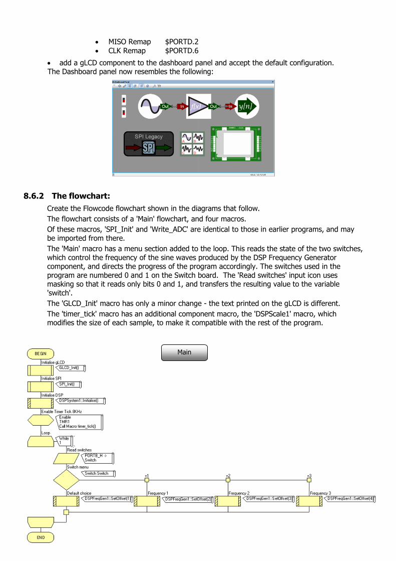
MISO Remap $PORTD.2
CLK Remap $PORTD.6
add a gLCD component to the dashboard panel and accept the default configuration. The Dashboard panel now resembles the following:
8.6.2 The flowchart:
Create the Flowcode flowchart shown in the diagrams that follow.
The flowchart consists of a 'Main' flowchart, and four macros.
Of these macros, 'SPI_Init' and 'Write_ADC' are identical to those in earlier programs, and may be imported from there.
The 'Main' macro has a menu section added to the loop. This reads the state of the two switches, which control the frequency of the sine waves produced by the DSP Frequency Generator component, and directs the progress of the program accordingly. The switches used in the program are numbered 0 and 1 on the Switch board. The 'Read switches' input icon uses masking so that it reads only bits 0 and 1, and transfers the resulting value to the variable 'switch'.
The 'GLCD_Init' macro has only a minor change - the text printed on the gLCD is different.
The 'timer_tick' macro has an additional component macro, the 'DSPScale1' macro, which modifies the size of each sample, to make it compatible with the rest of the program.
Main

Save the program as 'Exercise 4'.
GLCD_Init timer_tick
SPI_Init Write_DAC
8.6.3 The hardware:
Check that the dsPIC EB091 programmer jumper settings are the same as in program 1.
Connect the gLCD E-Blocks board, EB084, to Port B 0-7. Provide power for the board by connecting the '+V' screw terminal to the '+V' screw terminal on the EB091 programmer.
The jumper settings are the same as in program 1.
Connect the E-Blocks Switch board, EB007, to Port B 8-15. Provide power for the board by connecting the '+V' screw terminal to the '+V' screw terminal on the EB091 programmer.
The DSP Input E-Blocks board is not used in this program, but can be left in place, connected to the IDC cable.
Connect the DSP Output E-Blocks board, EB086, to the other connector on the dual E-Blocks IDC cables, plugged into Port D 0-7. Make sure to supply power by connecting the '+V' screw terminal to the '+V' screw terminal on the EB091 programmer.
Configure the jumpers as follows: Patch system jumper - patch position; Low-pass filter selection jumper - Bypass; Speaker / Line out selection jumper - Speaker; PWM / DAC input selection jumper - DAC.
Connect the EB091 programmer to the PC with a USB cable inserted in the “GHOST” USB socket.
Connect the universal power supply, HP2666, to the EB091 programmer - the green 'Power' LED will light.
Next, compile the program 'Exercise 4' and transfer it to the dsPIC chip.
8.6.4 Testing:
Simulation:
Simulate the program as follows:
From the 'View' menu, select the 'Scope' option. Position the Data Scope near the bottom the screen, and resize if necessary.
Start the simulation (by clicking on the icon, or pressing the F5 key);
Use the vertical scroll bars to locate the traces for 'AudioSignal' and 'AudioScaled'.
When you pause, or stop the simulation, you can examine these traces in more detail. (Pause the simulation by clicking on the icon, or by pressing the F7 key. Stop the
simulation by using the key or by pressing the Shift and F5 keys together.)
Click and hold the left mouse button, and move the cursor along the 'Trace navigation' bar to scroll horizontally through the trace.
Click and hold the left mouse button, and move the cursor down the 'Trace zoom' scale to zoom into the trace (change the time axis scale).

(Alternatively, instead of holding down the left mouse button, hold down the 'Ctrl' key and turn the mouse wheel.)
If you zoom in sufficiently, you will see that the waveform is digitised, as you will be able to resolve the individual digital data points that make it up.
Test the effect of 'closing' switches 0 and 1, both individually and together. They should create different frequencies on the Data Scope traces.
Hardware:
When you run the program on the dsPIC itself, you should hear a (fairly) pure tone produced by the loudspeaker.
Test the effect of closing switches 0 and 1, both individually and together. They should create different audio tones from the speaker, as the signal frequency changes.
Modify the program by changing the 'Waveform - Type' setting to 'Square', in the Frequency Generator properties. Download the new program, and listen to the sound produced. It is harsher.
Do the same for the other types of waveform.
Examine the waveforms on an oscilloscope attached to one of these points on the DSP Output board:
Audio In; Audio Gain;
Audio Filtered.

8.6.5 The Flowcode program in detail
The task is:
to take in a sample from the Frequency generator component;
convert it from 8-bit format to 16-bit format;
output the result from the dsPIC to the DAC on the DSP Output board;
send the DAC output to the speaker on the DSP Output board.
Main macro:
has much the same function as in previous programs, but it includes a 'switch' icon to change the frequency of the output signal, depending on which switches are pressed. It does so by changing the 'Period Offset' property of the Frequency Generator component, so that:
pressing no switches gives a period offset value of '1' - no change to the frequency;
pressing switch 0 gives a period offset value of '2' - twice the frequency;
pressing switch 1 gives a period offset value of '3' - three times the frequency;
pressing both switches gives a period offset value of '4' - four times the frequency;
GLCD_Init:
sets up the graphical LCD to display the message "4. Sine Generator":
timer_tick:
is triggered when Timer 1 overflows, and creates a new 'tick'. It then stores the next sample in the 'AudioSignal' buffer;
component macro 'LeftShiftTick' moves all bits of the sample eight place to the left in the buffer, effectively converting it into a 16-bit sample;
the result is stored in the DSP output buffer, and then transferred to the 'Data' variable by the component macro 'ReadRawTick';
the 'Write_DAC' macro is called to transfer this value to the DAC;
the 'TickAllBuffers' component macro now moves onto the next sample taken from the Frequency Generator.
SPI_Init:
enables SPI peripheral to control data transfer between the microcontroller and the DAC.
Write_DAC:
transfers the processed sample from the microcontroller to the DAC.
8.7 Further work
Click on the Frequency Generator component to make visible the component's properties.
Change the 'Waveform Type' to 'Sawtooth'.
Delete the data in the 'Waveform Data' section, and click 'Return'.
Click on the new data, right-click on the mouse, and select 'Copy'.
Open a spreadsheet application, and paste the data into it.
Then create a graph using that data, to check the shape produced.
Click on the Frequency Generator component again.
Change the 'Waveform Type' to 'Custom'.
Create data for your customised wave by typing in a series of numbers, each between 0 and 255.
Save the program, download it to the dsPIC, and listen to your synthesised notes!
Click on the Frequency Generator component again.
Change the 'Waveform Type' to 'White Noise'.
Save the program, download it to the dsPIC, and listen to the result.

9 Program 5 - Waveform generator
9.1 Introduction
This program extends the functionality of the previous one by allowing the user to select the waveform of the output signal using switches on the Switch E-Blocks board. Although it was possible to change the waveform with the previous program, it required a modification to the program and a fresh download to the dsPIC to effect the change. Here, it can be done while the program is running.
9.2 Objective
To generate signals whose waveform is selected using switches.
9.3 Requirements
This exercise requires:
a dsPIC EB091 programmer.
a copy of Flowcode 6 (or later) running on the PC
a DSP Output E-Block (EB086)
a graphical LCD E-Block (EB084)
a E-Block Switch board (EB007)
a universal power supply.
9.4 Flowcode program outline
The aim of the program is to:
initialise:
the DSP system;
the graphical LCD;
the SPI component.
sense the state of the switches;
generate a signal from the DSP Frequency Generator component, with either sinusoidal, square or triangular waveform, depending on the switch selection.
process it with the dsPIC
scale the signal data;
transfer the result to the output buffer.
transfer the result to the DAC, and then pass the signal produced to the speaker on the DSP output board;
display the name of the program "5. Waveform Generator" on the gLCD.

9.5 The system components
The flowchart controls eleven components:
the DSP System component, called 'DSPSystem1';
four Frequency Generator components, called 'DSPFreqGen1', 'DSPFreqGen2', 'DSPFreqGen3' and 'DSPFreqGen4';
the Scale component, called 'DSPScale1';
the Output component, called 'DSPOutput1';
the SPI component;
the graphical LCD component;
two switches on the E-Blocks Switch Board, called 'sw_slide_sub_pcb1' and 'sw_slide_sub_pcb2'.
Most of these have been described earlier. The notes that follow describe any new components, and any distinctive features of the others in this program.
9.5.1 The DSP Frequency Generator components
All four Frequency Generator components generate signals, with an amplitude of 200 units and a frequency of 160Hz.
'DSPFreqGen1' generates sinusoidal signals;
'DSPFreqGen2' generates square wave signals;
'DSPFreqGen3' generates triangular signals;
'DSPFreqGen4' generates sawtooth signals;
9.6 Creating the program
Write the Flowcode program using the following steps as a guide:
create a new Flowcode flowchart;
select the EB091 (from PIC16 pack) as a target;
9.6.1 The Dashboard panel:
add a DSP System component to the Dashboard panel;
configure it as follows:
Handle DSPSystem1; Buffer count 2; Simple mode No; Buffer A name AudioSignal;
Buffer B name AudioScaled;
Buffer A: Bit depth 8-bit; Sign Unsigned; Size 1;
Buffer B: Bit depth 16-bit; Sign Unsigned; Size 1.

add four DSP Frequency Generators to the Dashboard panel;
configure them as follows:
Frequency Generator 1:
Handle DSPFreqGen1; Buffer manager DSPSystem1; Output AudioSignal;
Type Sine; Amplitude 200; Offset 127; Period 50; Phase 0; Data Created automatically as you choose the waveform type; Period Offset 1.000000 Sample Rate 8000.000000.
Frequency Generator 2:
Handle DSPFreqGen1; Buffer manager DSPSystem1; Output AudioSignal; Type Square; Amplitude 200; Offset 0; Period 50; Phase 0; Data Created automatically as you choose the waveform type;
Period Offset 1.000000 Sample Rate 8000.000000.
Frequency Generator 3:
Handle DSPFreqGen1; Buffer manager DSPSystem1; Output AudioSignal; Type Triangle;
Amplitude 200; Offset 0; Period 50; Phase 0; Data Created automatically as you choose the waveform type; Period Offset 1.000000 Sample Rate 8000.000000.
Frequency Generator 4:
Handle DSPFreqGen1; Buffer manager DSPSystem1; Output AudioSignal; Type Sawtooth; Amplitude 200; Offset 0; Period 50; Phase 0; Data Created automatically as you choose the waveform type; Period Offset 1.000000
Sample Rate 8000.000000.

add a DSP Scale component to the Dashboard panel;
configure it as follows:
Handle DSPScale1; Buffer manager DSPSystem1; Input AudioSignal; Output AudioScaled.
add DSP Output component to the Dashboard panel;
configure it as follows:
Handle DSPOutput1; Buffer manager DSPSystem1; Output AudioScaled.
add SPI Master component to the Dashboard panel;
accept the default configuration except for:
Prescale FOSC / 16 MOSI Remap $PORTD.3 MISO Remap $PORTD.2 CLK Remap $PORTD.6
add a gLCD component to the dashboard panel and accept the default configuration.
The Dashboard panel resembles the following:

9.6.2 The flowchart:
Create the Flowcode flowchart shown in the following diagrams.
It consists of a 'Main' flowchart, and four macros - 'GLCD_Init', 'SPI_Init', 'Write_DAC' and 'timer_tick'. Of these, 'Main', 'SPI_Init' and 'Write_ADC' are identical to those in earlier programs, and may be imported from there.
The 'timer_tick' macro has a menu section added. This reads the state of the two switches, which control the waveform of the signals produced, by selecting the DSP Frequency Generator component, based on the state of the switches. Again, only switches '0' and '1' are used, and the 'Read switches' input icon uses masking to read only bits 0 and 1, and then transfers the result to the variable 'switch'.
The 'GLCD_Init' macro has only a minor change - the text printed on the gLCD is different.
Main GLCD_Init
timer_tick
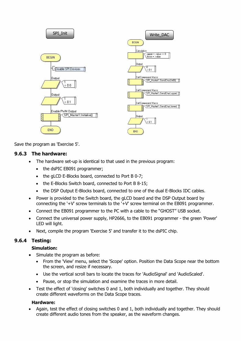
Save the program as 'Exercise 5'.
9.6.3 The hardware:
The hardware set-up is identical to that used in the previous program:
the dsPIC EB091 programmer;
the gLCD E-Blocks board, connected to Port B 0-7;
the E-Blocks Switch board, connected to Port B 8-15;
the DSP Output E-Blocks board, connected to one of the dual E-Blocks IDC cables.
Power is provided to the Switch board, the gLCD board and the DSP Output board by connecting the '+V' screw terminals to the '+V' screw terminal on the EB091 programmer.
Connect the EB091 programmer to the PC with a cable to the “GHOST” USB socket.
Connect the universal power supply, HP2666, to the EB091 programmer - the green 'Power' LED will light.
Next, compile the program 'Exercise 5' and transfer it to the dsPIC chip.
9.6.4 Testing:
Simulation:
Simulate the program as before:
From the 'View' menu, select the 'Scope' option. Position the Data Scope near the bottom the screen, and resize if necessary.
Use the vertical scroll bars to locate the traces for 'AudioSignal' and 'AudioScaled'.
Pause, or stop the simulation and examine the traces in more detail.
Test the effect of 'closing' switches 0 and 1, both individually and together. They should create different waveforms on the Data Scope traces.
Hardware:
Again, test the effect of closing switches 0 and 1, both individually and together. They should create different audio tones from the speaker, as the waveform changes.
SPI_Init Write_DAC

9.6.5 The Flowcode program in detail
The task is:
to take in a sample from the selected Frequency Generator component;
convert it from 8-bit format to 16-bit format;
output the result from the dsPIC to the DAC on the DSP Output board;
send the DAC output to the speaker on the DSP Output board.
Main macro:
has much the same function as in the previous program.
GLCD_Init:
sets up the graphical LCD to display the message "5. Waveform Generator":
timer_tick:
is triggered when Timer 1 overflows, and creates a new 'tick';
it then reads the status of the switches, storing the result in the variable 'switch';
it uses this value to select a Frequency Generator component;
it stores the next sample from the selected Frequency Generator in the 'AudioSignal' buffer;
the component macro 'LeftShiftTick' moves all bits of the sample eight place to the left in the buffer, effectively converting it into a 16-bit sample;
the result is stored in the DSP output buffer, and then transferred to the 'Data' variable by the component macro 'ReadRawTick';
the 'Write_DAC' macro is called to transfer this value to the DAC;
the 'TickAllBuffers' component macro now moves onto the next sample taken from the Frequency Generator.
SPI_Init:
enables SPI peripheral to control data transfer between the microcontroller and the DAC.
Write_DAC:
transfers the processed sample from the microcontroller to the DAC.
9.7 Further work
Click on each Frequency Generator component in turn to make visible the component's properties.
Modify the program by changing the 'Period Offset' settings to a different value for each.
Download the new program and listen to the sound produced.
Modify the original program so that:
pressing switches 0 and 1 together has no effect;
the sawtooth waveform is generated when switch 2 (alone) is pressed;
a sine wave with double the original frequency is produced by pressing switch 3 (alone);
a square wave with double the original frequency is produced by pressing switch 4 (alone).
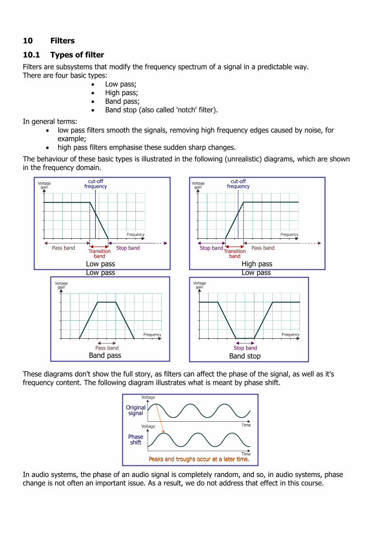
Band pass
10 Filters
10.1 Types of filter
Filters are subsystems that modify the frequency spectrum of a signal in a predictable way. There are four basic types:
Low pass; High pass; Band pass; Band stop (also called 'notch' filter).
In general terms:
low pass filters smooth the signals, removing high frequency edges caused by noise, for example;
high pass filters emphasise these sudden sharp changes.
The behaviour of these basic types is illustrated in the following (unrealistic) diagrams, which are shown in the frequency domain.
These diagrams don't show the full story, as filters can affect the phase of the signal, as well as it's frequency content. The following diagram illustrates what is meant by phase shift.
In audio systems, the phase of an audio signal is completely random, and so, in audio systems, phase change is not often an important issue. As a result, we do not address that effect in this course.
Low pass Low pass
High pass Low pass
Band stop
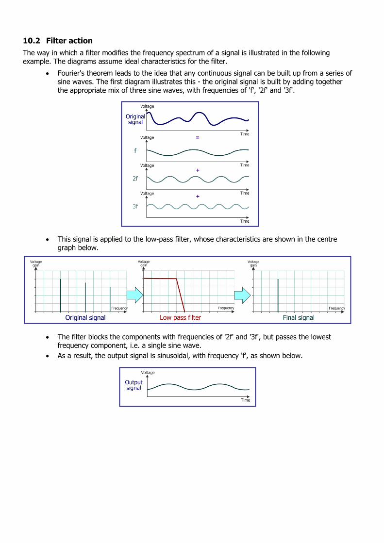
10.2 Filter action
The way in which a filter modifies the frequency spectrum of a signal is illustrated in the following example. The diagrams assume ideal characteristics for the filter.
Fourier's theorem leads to the idea that any continuous signal can be built up from a series of sine waves. The first diagram illustrates this - the original signal is built by adding together the appropriate mix of three sine waves, with frequencies of 'f', '2f' and '3f'.
This signal is applied to the low-pass filter, whose characteristics are shown in the centre graph below.
The filter blocks the components with frequencies of '2f' and '3f', but passes the lowest frequency component, i.e. a single sine wave.
As a result, the output signal is sinusoidal, with frequency 'f', as shown below.

10.4 Filter properties
The following terms can be used to describe and define the behaviour of a filter:
Linear - filters that obey superposition; If input 'A' produces output 'X', and input 'B' produces output 'Y', then input '(A + B)'
produces output '(X + Y)'.
Time-invariant - the performance of the filter does not change with time. The output of the filter may vary with time, since the input signal probably varies with
time. However, the filter kernel (its frequency response), does not change over time.
Gain - the amplification factor applied to the input signal at a certain frequency;
usually voltage gain ( = VOUT / VIN);
active filters, usually based on components like operational amplifiers, can provide a voltage gain > 1;
passive filters have a maximum voltage gain of 1;
is often expressed in decibels (dB);
Voltage gain in dB = 20 x log(Voltage gain as a ratio);
Bandwidth – the range of signal frequencies for which the filter has appreciable gain;
often measured between the 'half-power' points, the frequencies where the power in the signal has dropped to half its maximum value.
these points are where the voltage gain drops to 71% (=0.71) of its maximum value. (Voltage is easier to measure than power,)
measured in decibels, 20 x log(0.71) = -3dB roughly, so bandwidth is often measured as the range of frequencies between the '-3dB' points.
Cut-off frequency – the frequency where the gain is no longer appreciable; also referred to as –3 dB frequency.
Roll off - the rate at which the filter moves from the pass band to the stop band;
fast roll-off means that the transition band is very narrow.
often measured in decibels per octave (i.e. the change in gain for a doubling of the signal frequency. The next diagram shows three rates of roll off.
Interpretation of the diagram:
The greater the roll off, the more discriminating the filter - it rejects unwanted frequencies better.
0dB means a voltage gain of one - input and output signals have the same voltage.
6dB/octave - the amplitude halves when the frequency is doubled.
12dB/octave - the amplitude quarters when the frequency is doubled.
24db/octave - the amplitude reduces to 6% when the frequency is doubled.

10.3 Filter problems
Poor stop band attenuation:
results in poor rejection of unwanted frequencies;
Overshoot:
the voltage gain is temporarily higher than the intended final value; can often be the result of inputting a rapidly changing input signal; introduces distortion of the signal.
Ringing:
the voltage gain oscillates, but slowly decays away to the intended value; another source of signal distortion; once again, can be caused by transients (high amplitude, short-duration input signal).
Together, overshoot and ringing can result in undesirable echoes, particularly evident when processing signals rich in transients, such as those produced by percussion instruments.

11 Program 6 - Low pass filter
11.1 Introduction
This program introduces the topic of filtering - selecting certain frequencies and rejecting others. It uses a low-pass filter to allow sine wave signals to pass to the output only if they have a frequency below a set value.
11.2 Objective
To demonstrate the effect of a low-pass filter on sinusoidal signals with different frequencies.
11.3 Requirements
This exercise requires:
a dsPIC EB091 programmer.
a copy of Flowcode 6 (or later) running on the PC
a DSP Output E-Block (EB086)
a graphical LCD E-Block (EB084)
a E-Block Switch board (EB007)
a universal power supply.
11.4 Flowcode program outline
The aim of the program is to:
initialise:
the DSP system;
the graphical LCD;
the SPI component.
generate a digitised sine wave signal from the DSP Frequency Generator component, having a frequency dependent on the setting of two switches on the E-Blocks Switch board.
process it by:
scaling the signal to convert it to a 16-bit sample;
filtering it with a low-pass filter component;
transferring the result to the output buffer.
transfer the result to the DAC, and pass the signal produced to the speaker on the DSP Output board;
display the name of the program "6. Low Pass Filter" on the gLCD.

11.5 The system components
The flowchart controls nine components:
the DSP System component, called 'DSPSystem1';
the Frequency Generator component, called 'DSPFreqGen1';
the Scale component, called 'DSPScale1';
the DSP Filter component, called 'DSPFilter1';
the Output component, called 'DSPOutput1';
the SPI component;
the graphical LCD component;
two switches on the E-Blocks Switch Board, called 'sw_slide_sub_pcb1' and 'sw_slide_sub_pcb2'.
The notes that follow describe the new component, and any distinctive features of the others in this program.
11.5.1 The DSP Filter component
It is used to manipulate the frequency response of the DSP system.
Its properties can be changed to make it a low-pass filter (which stops high frequencies,) a high-pass filter (which stops low frequencies,) a band-pass filter, (which stops very high and very low frequencies, but passes frequencies in between,) a band-stop filter (which does the reverse of the band-pass filter,) and two others, the FIR and the IIR filter, which do not form part of this course.
Another of its properties is used to set the cut-off frequency, the boundary frequency at which the behaviour just described begins, by setting a coefficient, a numerical value, used in the formula:
Cut-off frequency = Nyquist frequency Coefficient
The Nyquist frequency is the highest signal frequency that can be sampled successfully, and is given by the formula:
Nyquist frequency = Sample rate 2
11.5.2 The switches
As in program 4, the switches are used to change the frequency of the output sinusoidal signal by altering the period offset value. These can produce twice, three times and four times the base frequency of 160Hz, and show the effect of the low-pass filter, which has a cut-off frequency of 200Hz.

11.6 Creating the program
Write the Flowcode program using the following steps as a guide:
create a new Flowcode flowchart;
select the EB091 (from PIC16 pack) as a target;
11.6.1 The Dashboard panel:
add a DSP System component to the Dashboard panel;
configure it as follows:
Handle DSPSystem1; Buffer count 3;
Simple mode Yes; Buffer A name AudioSignal; Buffer B name AudioScaled; Buffer C name AudioFiltered; Bit depth 16-bit; Sign Unsigned; Size 1.
add DSP Frequency Generator to the Dashboard panel;
configure it as follows:
Handle DSPFreqGen1; Buffer manager DSPSystem1; Output AudioSignal; Type Sine; Amplitude 200; Offset 127; Period 50; Phase 0; Data Created automatically as you choose the waveform type;
Period Offset 1.000000 Sample Rate 8000.000000.
add a DSP Scale component to the Dashboard panel;
configure it as follows:
Handle DSPScale1; Buffer manager DSPSystem1; Input AudioSignal;
Output AudioScaled.
add a DSP Filter component to the Dashboard panel;
configure it as follows:
Handle DSPFilter1; Buffer manager DSPSystem1; Input AudioScaled;
Output AudioFiltered; Type Low Pass; Coefficient 0 10; Sample Rate 8000.000000
add DSP Output component to the Dashboard panel;
configure it as follows:
Handle DSPOutput1;
Buffer manager DSPSystem1; Output AudioFiltered.

add SPI Master component to the Dashboard panel, (from the Comms toolbox);
accept the default configuration except for:
Prescale FOSC / 16 MOSI Remap $PORTD.3 MISO Remap $PORTD.2 CLK Remap $PORTD.6
add a gLCD component to the dashboard panel and accept the default configuration.
The Dashboard panel resembles the following:
Note - This is identical to the Dashboard panel for the previous program, except for the symbol for the Filter component.
11.6.2 The flowchart:
Create the Flowcode flowchart shown in the following diagrams.
It consists of a 'Main' flowchart, and four macros - 'GLCD_Init', 'SPI_Init', 'Write_DAC' and 'timer_tick'. Of these macros, 'SPI_Init' and 'Write_ADC' are identical to those in earlier programs, and may be imported from there.
The 'Main' macro is identical to that used in program 6.
The 'GLCD_Init' macro has only a minor change - the text printed on the gLCD is different.
The 'timer_tick' macro has an additional component macro, to control the DSP Filter component.
Main

Save the program as 'Exercise 6'.
11.6.3 The hardware:
The hardware set-up is identical to that used in the last two programs:
the dsPIC EB091 programmer;
the gLCD E-Blocks board, connected to Port B 0-7;
the E-Blocks Switch board, connected to Port B 8-15;
the DSP Output E-Blocks board, connected to one of the dual E-Blocks IDC cables.
Power is provided to the Switch board, the gLCD board and the DSP Output board by connecting the '+V' screw terminals to the '+V' screw terminal on the EB091 programmer.
Connect the EB091 programmer to the PC with a cable to the “GHOST” USB socket .
Connect the universal power supply, HP2666, to the EB091 programmer - the green 'Power' LED will light.
GLCD_Init timer_tick
SPI_Init Write_DAC

Next, compile program 'Exercise 6' and transfer it to the dsPIC chip.
11.6.4 Testing:
Simulation:
Simulate the program as before:
Position the Data Scope near the bottom the screen, and resize if necessary.
Use the vertical scroll bars to locate the traces for 'AudioScaled' and 'AudioFiltered'. (The 'AudioSignal' trace shows only a flat line, as it is produced in 8-bit format, which is tiny on the scale used in the Data Scope.)
Pause, or stop the simulation and examine the traces in more detail.
Test the effect of 'closing' switches 0 and 1, both individually and together, to increase the frequency of the signal, from 160Hz, to 320Hz, 480Hz and 640Hz.
As you do so, the 'AudioFiltered' trace gets smaller, as the filter cuts out frequencies above the cut-off frequency of 400Hz.
Hardware:
Again, test the effect of closing switches 0 and 1, both individually and together. They should create different audio tones from the speaker, which get quieter as the frequency increases.
11.6.5 The Flowcode program in detail
The task is:
to take in a sample from the Frequency Generator component;
convert it from 8-bit format to 16-bit format;
process it with the DSP Filter component;
output the result from the dsPIC to the DAC on the DSP Output board;
send the DAC output to the speaker on the DSP Output board.
Main macro: has much the same function as in program 4.
reads the status of the switches, storing the result in the variable 'switch';
uses this value to select the value of the 'Period Offset' property, which then determines the frequency of the signal produced by the Frequency Generator component.
GLCD_Init: sets up the graphical LCD to display the message "6. Low Pass Filter":
timer_tick: is triggered when Timer 1 overflows, and creates a new 'tick';
it stores the next sample from the selected Frequency Generator in the 'AudioSignal' buffer;
the component macro 'LeftShiftTick' converts it into a 16-bit sample, and stores the result in the 'AudioScaled' buffer;
the component macro 'FilterTick' performs the filter operation on this sample, and stores the result in the 'AudioFiltered' buffer;
this is passed to the DSP Output component, which executes the component macro 'ReadRawTick' to transfer it to the 'Data' variable;
the 'Write_DAC' macro transfers this value to the DAC;
the 'TickAllBuffers' component macro now moves onto the next sample taken from the Frequency Generator.
SPI_Init:
enables SPI peripheral to control data transfer between the microcontroller and the DAC.
Write_DAC:
transfers the processed sample from the microcontroller to the DAC.
11.7 Further work
Click on the DSP Frequency Generator component;
Modify the program by changing the 'Waveform Type' setting to a different waveform.
Simulate the program, and view the effect of the filter on the signal using the Data Scope.
Interpret what happens. (Remember - other waveforms have a more complex frequency spectrum, and contain a range of harmonics at higher frequencies. The low-pass filter will have a greater effect on these than on lower frequencies.)
Download the new program and listen to the sound produced. Is it as 'harsh' as the raw waveform?
Click on the DSP Filter component;
Change the 'Coefficient' setting to a different value (say '1') to increase the cut-off frequency.
Simulate the program, and view the effect of the filter on the signal using the Data Scope.
Download the new program and listen to the sound produced.
Explain any differences.

12 Digital filters
12.1 Analogue versus digital filters
Filters can be made in two basic ways:
using analogue hardware;
implementing equations using a software program in a digital system, such as a dsPIC.
Analogue filters:
built from resistors, capacitors, and inductors, low cost components, and so are cheap;
accept a wide range of both amplitudes and frequencies;
but
component values have tolerances, (i.e. are made to a certain accuracy), making the result unpredictable from one filter to another;
properties are temperature dependent.
Digital filters:
can achieve higher accuracy and greater reliability. Accuracy is determined by factors like the resolution of the ADC, and the number of bits used to describe the data.
produce outputs which can be stored easily, in memory. Analogue data can be stored, on magnetic tape, for example, but is then prone to added noise from the storage process.
can be designed to eliminate the filter problems outlined in section 10.3;
can be re-designed more easily, as this usually involves changes in software, not in hardware;
produce results which are sensitive to electrical noise;
but
generate signals which include quantisation error;
can introduce latency;
have outputs prone to contain aliasing frequencies.
12.2 Digital filters
Uses of digital filters can be divided into two general areas:
Removal of unwanted frequency components such as: electrical noise;
electrical interference from other signal sources.
Removal of distortion caused by:
hardware imperfections;
system non-linearity.
Their excellent performance leads to widespread use in:
audio and speech manipulation;
modems;
video and optical image processing;
motor control systems.
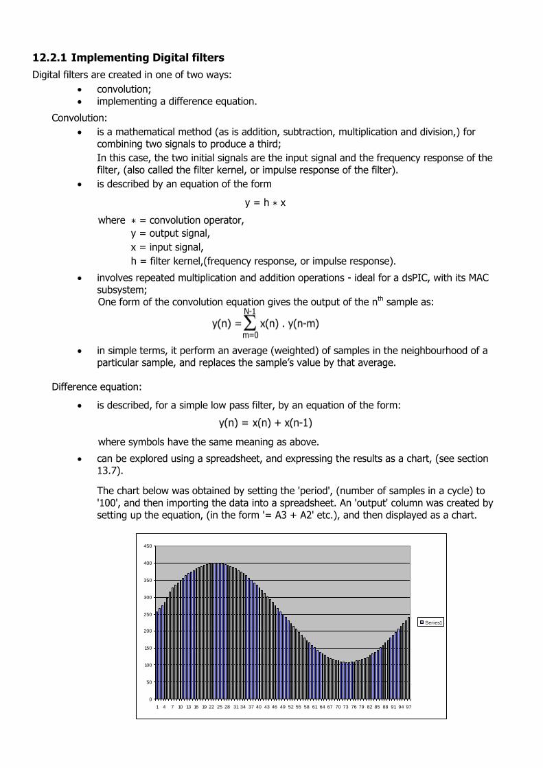
0
50
100
150
200
250
300
350
400
450
1 4 7 10 13 16 19 22 25 28 31 34 37 40 43 46 49 52 55 58 61 64 67 70 73 76 79 82 85 88 91 94 97
Series1
12.2.1 Implementing Digital filters
Digital filters are created in one of two ways:
convolution; implementing a difference equation.
Convolution:
is a mathematical method (as is addition, subtraction, multiplication and division,) for combining two signals to produce a third;
In this case, the two initial signals are the input signal and the frequency response of the filter, (also called the filter kernel, or impulse response of the filter).
is described by an equation of the form
y = h * x
where * = convolution operator,
y = output signal,
x = input signal,
h = filter kernel,(frequency response, or impulse response).
involves repeated multiplication and addition operations - ideal for a dsPIC, with its MAC subsystem;
One form of the convolution equation gives the output of the nth sample as:
in simple terms, it perform an average (weighted) of samples in the neighbourhood of a particular sample, and replaces the sample’s value by that average.
Difference equation:
is described, for a simple low pass filter, by an equation of the form:
where symbols have the same meaning as above.
can be explored using a spreadsheet, and expressing the results as a chart, (see section 13.7).
The chart below was obtained by setting the 'period', (number of samples in a cycle) to '100', and then importing the data into a spreadsheet. An 'output' column was created by setting up the equation, (in the form '= A3 + A2' etc.), and then displayed as a chart.

13 Program 7 - High pass filter
13.1 Introduction
Still on the topic of filtering, this program demonstrates the use of a high-pass filter to allow sine wave signals to pass to the output only if they have a frequency above a set value.
13.2 Objective
To demonstrate the effect of a high-pass filter on sinusoidal signals with different frequencies.
13.3 Requirements
This exercise requires:
a dsPIC EB091 programmer.
a copy of Flowcode 6 (or later) running on the PC
a DSP Output E-Block (EB086)
a graphical LCD E-Block (EB084)
a E-Block Switch board (EB007)
a universal power supply.
13.4 Flowcode program outline
The aim of the program is to:
initialise:
the DSP system;
the graphical LCD;
the SPI component.
generate a sine wave signal from the DSP Frequency Generator component with a frequency determined by the setting of two switches on the E-Blocks Switch board.
process it by:
scaling the signal to convert it to a 16-bit sample;
filtering it with a high-pass filter component;
transferring the result to the output buffer.
copy the result to the DAC, and pass the output produced to the speaker on the DSP Output board;
display the name of the program "7. High Pass Filter" on the gLCD.
13.5 The system components
The flowchart controls nine components:
the DSP System component, called 'DSPSystem1';
the Frequency Generator component, called 'DSPFreqGen1';
the Scale component, called 'DSPScale1';
the DSP Filter component, called 'DSPFilter1';
the Output component, called 'DSPOutput1';
the SPI component;
the graphical LCD component;
two switches on the E-Blocks Switch Board, called 'sw_slide_sub_pcb1' and 'sw_slide_sub_pcb2'.

There are no new components in this program. These notes describe any distinctive features of the others in this program.
13.5.1 The DSP Filter component
The properties are identical to those in the previous program, except that, this time, it is configured as a high-pass filter. The cut-off frequency is adjusted to match the range of frequencies generated by the DSP Frequency Generator.
13.5.2 The switches
As in programs 4 and 6, the switches are used to change the frequency of the output sinusoidal signal by altering the period offset value.
13.6 Creating the program
Write the Flowcode program using the following steps as a guide:
create a new Flowcode flowchart;
select the EB091 (from PIC16 pack) as a target;
13.6.1 The Dashboard panel:
add a DSP System component to the Dashboard panel;
configure it in the same way as in program 6:
Handle DSPSystem1; Buffer count 3; Simple mode Yes; Buffer A name AudioSignal; Buffer B name AudioScaled; Buffer C name AudioFiltered; Bit depth 16-bit; Sign Unsigned; Size 1.
add DSP Frequency Generator;
configure it in the same way as before:
Handle DSPFreqGen1; Buffer manager DSPSystem1; Output AudioSignal; Type Sine; Amplitude 200; Offset 127;
Period 50; Phase 0; Data Created automatically as you choose the waveform type; Period Offset 1.000000 Sample Rate 8000.000000.
add a DSP Scale component;
configure it as follows:
Handle DSPScale1; Buffer manager DSPSystem1; Input AudioSignal; Output AudioScaled.

add a DSP Filter component;
configure it as follows:
Handle DSPFilter1; Buffer manager DSPSystem1; Input AudioScaled; Output AudioFiltered; Type High Pass; Coefficient 0 2; Sample Rate 8000.000000
add DSP Output component;
configure it as follows:
Handle DSPOutput1; Buffer manager DSPSystem1; Output AudioFiltered.
add SPI Master component;
accept the default configuration except for:
Prescale FOSC / 16
MOSI Remap $PORTD.3 MISO Remap $PORTD.2 CLK Remap $PORTD.6
add a gLCD component and accept the default configuration.
The Dashboard panel resembles the following:

13.6.2 The flowchart:
Create the Flowcode flowchart shown in the following diagrams.
It consists of a 'Main' flowchart, and four macros. Of these, 'SPI_Init' and 'Write_ADC' are identical to those in earlier programs, and may be imported from there.
The 'Main' macro and 'timer_tick' macro are identical to that in program 6.
The 'GLCD_Init' macro has different text printed on the gLCD screen.
Main
GLCD_Init timer_tick

Save the program as 'Exercise 7'.
13.6.3 The hardware:
The hardware set-up is identical to that used in the previous programs:
the dsPIC EB091 programmer;
the gLCD E-Blocks board, connected to Port B 0-7;
the E-Blocks Switch board, connected to Port B 8-15;
the DSP Output E-Blocks board, connected to one of the dual E-Blocks IDC cables.
Power is provided to the Switch board, the gLCD board and the DSP Output board by connecting the '+V' screw terminals to the '+V' screw terminal on the EB091 programmer.
Connect the EB091 programmer to the PC with a cable to the “GHOST” USB socket.
Connect the universal power supply, HP2666, to the EB091 programmer - the green 'Power' LED will light.
Next, compile program 'Exercise 7' and transfer it to the dsPIC chip.
13.6.4 Testing:
Simulation:
Simulate the program as before:
Position the Data Scope near the bottom the screen, and resize if necessary.
Use the vertical scroll bars to locate 'AudioScaled' and 'AudioFiltered' and ignore the 'AudioSignal' trace for the same reason as that given in program 6.
Pause, or stop the simulation and examine the traces in more detail.
Test the effect of 'closing' switches 0 and 1, both individually and together, to increase the frequency of the signal, from 160Hz, to 320Hz, 480Hz and 640Hz.
Notice the amplitude of the 'AudioFiltered' trace as you do so. (Remember - the filter cut-off frequency is 2000Hz for this program.)
Hardware:
Again, test the effect of closing switches 0 and 1, both individually and together. They should create different tones and loudness levels as the frequency increases.
SPI_Init Write_DAC

13.6.5 The Flowcode program in detail
The task is very similar to that in program 6:
to take in a sample from the Frequency Generator component;
convert it from 8-bit format to 16-bit format;
process it with the DSP Filter component;
output the result from the dsPIC to the DAC on the DSP Output board;
send the DAC output to the speaker on the DSP Output board.
Main macro: has much the same function as in program 4.
reads the status of the switches, storing the result in the variable 'switch';
uses this value to select the value of the 'Period Offset' property, which then determines the frequency of the signal produced by the Frequency Generator component.
GLCD_Init: sets up the graphical LCD to display the message "7. High Pass Filter":
timer_tick: is triggered when Timer 1 overflows, and creates a new 'tick';
it stores the next sample from the selected Frequency Generator in the 'AudioSignal' buffer;
the component macro 'LeftShiftTick' converts it into a 16-bit sample, and stores the result in the 'AudioScaled' buffer;
the component macro 'FilterTick' performs the filter operation on this sample, and stores the result in the 'AudioFiltered' buffer;
this is passed to the DSP Output component, which executes the component macro 'ReadRawTick' to transfer it to the 'Data' variable;
the 'Write_DAC' macro transfers this value to the DAC;
the 'TickAllBuffers' component macro now moves onto the next sample taken from the Frequency Generator.
SPI_Init: enables SPI peripheral to control data transfer between the microcontroller and the DAC.
Write_DAC:
transfers the processed sample from the microcontroller to the DAC.
13.7 Further work
Click on the DSP Frequency Generator component;
Modify the program by changing the 'Waveform Type' setting to a different waveform.
Simulate the program, and view the effect of the filter on the signal using the Data Scope.
Interpret what happens.
Download the new program and listen to the sound produced. Is it as 'harsh' as the raw waveform?
Click on the DSP Filter component;
Change the 'Coefficient' setting to a different value (say 10) to reduce the cut-off frequency.
Simulate the program, and view the effect of the filter on the signal using the Data Scope.
Download the new program and listen to the sound produced.
Explain any differences.
Congratulations! You've finished the course.

14. Instructor Guide
14.1
Introduction
The course is essentially a practical one. The E-Blocks hardware makes it simple and quick to
program, construct and test microcontroller circuits.
14.2
Aim
The course extends knowledge of the graphical programming language Flowcode 6 (or later),
to its use in programming dsPIC microcontrollers.
14.3
Prior Knowledge
It is advisable that the student understands and has experience of programming a standard
microcontroller, using Flowcode 6 (or later).
14.4 Learning Objectives
On successful completion of this course, the student will be able to:
run the Flowcode 6 (or later) application;
describe the nature of human hearing, state the audio frequency range and explain what is meant
by 'fundamental' and 'harmonics';
compare and distinguish between analogue and digital signals;
explain what is meant by sampling, and give one disadvantage of its use;
explain what is meant by aliasing, and give an example of its occurrence;
state the Nyquist sampling criterion, and explain its link to aliasing;
describe the function of analogue-to-digital converters and list factors affecting resolution;
draw a sketch to illustrate the meaning of 'a sample-and-hold output';
describe the function of a digital-to-analogue converter ;
explain the following terms used in connection with DAC's
- resolution, maximum sampling rate, monotonicity and dynamic range.
construct a DSP system, consisting of:
a dsPIC EB091 programmer E-Blocks board, containing a dsPIC microcontroller;
a DSP Input E-Blocks (EB085) board;
a DSP Output E-Blocks (EB086) board; a E-Blocks graphical LCD (EB084) board;
a E-Blocks Switch (EB007) board.
create a Flowcode 6 (or later) flowchart, using the following functions:
Input, Output, Loop, Calculation, Decision and 'Switch';
Macro, Component Macro and Interrupt;
and the following components:
DSP System, Input, Output and Frequency Generator components;
DSP Scale, Sum, Delay, and Filter components;
SPI, GLCD and Switch components.
simulate a Flowcode 6 (or later) flowchart, and view the signals produced on the 'Data Scope'.
describe the role of the DSP System component as buffer manager;
describe the role of buffers in the DSP system;
explain how the on-board timer overflows cause the program to progress;
describe the role of the SPI component;
add DSP and related components to the Dashboard panel, and configure them;
configure the jumper settings of the E-Blocks hardware;
use the EB091 programmer board to provide power to the satellite E-Blocks boards;
devise a testing regime for the Flowcode 6 (or later) programs;
use a Calculation function to convert a sample from 8-bit into 16-bit;
modify the text displayed on the graphical LCD;
distinguish between a microprocessor, a microcontroller and a DSP microcontroller;
describe the meaning of 'pipelining' and 'dynamic pipelining';
describe the following DSP system features:
hardware multipliers accumulators and MAC hardware;
barrel shifters;
circular buffers;
direct memory access.
explain what is meant by 'modulo' and 'bit-reversed' addressing, and 'saturation logic';
explain the terms 'echo' and 'reverberation', when applied to audio signals;
describe the role of the DSP Scale, Sum and Delay components, in echo and reverberation;
configure the bit-depth and type of buffer using the 'Properties' pane;
compare the general features of the following communication protocols - SPI, !2C and UART.
distinguish between 'time domain' and 'frequency domain' descriptions of a signal;
explain what is meant by 'electrical noise';
distinguish between 'pink' noise and 'white' noise;
recognise the following waveforms, from time domain graphs:
sinusoidal;
square;
pulse;
triangular;
sawtooth.
draw the frequency spectrum for a sinusoidal signal;
configure the following properties of a Frequency Generator component:
waveform type;
amplitude;
offset;
period;
phase;
period offset.
explain the role of the 'period offset' value in changing the frequency of the signal produced;
calculate the period and frequency, given the number of samples in each cycle and the sample
rate;
create a Flowcode 6 (or later) flowchart section to allow the frequency of the signal produced by a
Frequency Generator component, or its waveform, to be selected by switches;
recognise the following filter types from their frequency spectra - low pass, high pass, band pass
and band stop.
draw voltage/time graphs for a sinusoidal signal to explain what is meant by 'phase';
draw frequency spectra to illustrate the action of a filter;
explain the following terms, used to describe filters:
pass band, transition band and stop band;
linear, time-invariant;
gain ,bandwidth, roll-off andcut-off frequency;
identify on a frequency spectrum graph, and explain the unwanted consequences of poor stop
band attenuation, overshoot and ringing.
use the relationship between Nyquist criterion and filter coefficient to configure the cut-off
frequency for a Filter component;
compare the performance of analogue and digital filters;
outline the two ways, using convolution or using difference equations, to implement a digital filter.

14.5 What the student will need:
To complete the course, the student will need the following:
Flowcode 6 (or later) software
E-blocks including: a dsPIC EB091 programmer
a DSP Input E-block (EB085)
a DSP Output E-block (EB086)
a Switch unit E-block (EB007)
a Graphical LCD E-Block (EB084)
a high impedance microphone and earpiece
a universal power supply (HP2666)
14.6 Time:
It will take students between twelve and sixteen hours to complete the worksheets.
Additional time will be needed to study the background concepts, depending on the students'
experience and prior knowledge.
14.7 Further information:
This course contains all the information you need to gain a firm foundation in the use of
Flowcode 6 (or later) with the dsPIC. You are urged to look at the extensive volume of
information and examples contained in the Matrix wiki, found at www.matrixtsl.com/wiki to
expand your knowledge and experience.

15. Scheme of work
Section Notes for the Instructor Timing
1
The introduction gives a brief overview of Digital Signal Processing, and gives the block diagram of a simple DSP system.
To remind students of what they almost certainly met in secondary science, the topic of sound and hearing is re-visited. Where students have not studied these topics previously, it may be necessary for the instructor to give a detailed presentation on the topic.
Although the world seems obsessed with turning everything digital, analogue signals still have their place. The next section compares the two.
One consequence of using digital processing is that the analogue quantity must be sampled. This involves making a measurement of , say, the signal voltage periodically, and then processing these samples. Sampling can be the Achilles' heel of digital processing, as it can conceal real aspects of the signal, and, equally, introduce others that do not exist in the original signal. It is important to use an appropriate sampling frequency for the signal under investigation. Too high a sample-rate adds to the processing burden, and can slow it down by an unacceptable amount. Too low, and aliasing becomes a problem, as well as the quality of the processed signal. Traditionally, telephone services struck a happy medium at 8000 samples per second. The resulting audio is intelligible, but by no means hi-fi. However, the task of processing these signals is manageable.
The course briefly discusses the Nyquist sampling theorem, and its effect on aliasing. The following topics are analogue-to-digital and digital-to-analogue conversion. The aim of these is straightforward, but there are many ways to implement that aim, and they go beyond the scope of this course.
The instructor may wish, at this point, to elaborate on the techniques involved in these conversions. At a minimum, it is recommended that the vocabulary of these converters is explained, ideally with reference to the AD7680 and the AD5662 devices used on the DSP Input and Output boards.
To enhance their understanding, students could be encouraged to research topics such as analogue-to-digital and digital-to-analogue conversion, using resources such as the internet, and could be required to create presentations on topics like these for their colleagues.

2 2
The main objective of the first program is to familiarise the students with the software and hardware. Although not apparently an intricate task, it brings out a range of digital signal processing techniques.
First of all, the ADC converts the analogue audio signal to digital. The dsPIC then takes a sample each time the on-board timer overflows. The result is passed to the output buffer, and from there to the DAC on the DSP Output board, where it is converted back to an analogue signal. This is then outputted to the earpiece or speaker.
Much of the preparation for this has already taken place, in looking at sampling, and at ADC's and DAC's in section 1. Section 2 starts by examining the functions of the DSP System, Input and Output components, and the SPI and GLCD components. It may be that students need help with the concept of a buffer. It is effectively a 16-bit shift register, which talks to the processor in parallel fashion, but talks to the peripherals in serial mode.
What may not be apparent is the role of the timer. The Main program plays only a minor role. After initialising the GLCD, and the SPI and DSP subsystems, it simply keeps looping indefinitely - not doing anything, just looping. The SPI subsystem is used to control communication between the dsPIC (the master) and the ADC and DAC (the slaves). The ADC SPI link is enabled by applying a logic 0 signal to its enable pin, Port D bit 0. The DAC SPI is enabled in similar fashion on Port D bit 1. The 'SPI_Init' macro starts by disabling both, by setting both Port D bit 0 and bit 1.
The real work is done by the interrupt routine. Every time the onboard timer overflows (exceeds its maximum count,) it generates an interrupt, which causes the processor to run through the 'timer_tick' macro. In the language of DSP, the 'tick' it creates triggers the system to read and process the next sample, and then increments the pointers to the subsequent samples in all the buffers, (actually, only one in this program).
There are two modes for reading the buffers, either the system processes one sample from the buffer at a time, or it reads the contents of the whole buffer, and then processes it. The latter is called simply a 'Function' macro. It involves a loop to cycle through all locations in the buffer, performing the macro's functionality. The former is called a 'Function tick' macro. This performs the macro's functionality on the value from a single location in the buffer. The 'TickAllBuffers' macro moves the buffer pointers to the next sample.
The 'Read_ADC' and 'Write_DAC' macros start by enabling the respective devices by applying logic 0 to the enable pin. The rest is concerned with formatting the 8-bits of data from the SPI bus, to make it compatible with the ADC and DAC, both of which expect 24 bytes of data. This conversion is done inside the Calculation icons. The text attempts to illustrate one of these conversions, but it may need extra input from the instructor to drive home the significance of what is happening.
As these macros, and the 'SPI_Init' macro, are re-used, unchanged, in later programs, it is worth exporting them to an area accessible to the students, so that they can later import them, to save time.
Testing takes place solely on the hardware. If there is a problem, then it is worth checking the jumper settings, and checking that the peripheral boards are powered from the EB091 programmer. A separate microphone and earpiece make testing easier than using the microphone and speaker on the DSP Input and Output boards.
The instructor could test the student's grasp of the program by asking for an explanation of the role of a selection of the icons in the flowchart.
30-40 mins

3
This section examines aspects of digital signal processing, and highlights differences between microprocessors, microcontrollers and digital signal microprocessors. Only a minority of students should find this discussion difficult. The important issue is that DSC's are built for speed. They operate in real time, and at high sample rates, and so the processing must create as little latency as possible. The majority of tasks carried out by a DSC could be done on a standard microcontroller, but would not be done so quickly.
There follows an exploration of the meaning of pipelining, an important technique in many processors. The instructor may wish to expand this treatment to ensure that its significance is driven home.
After that, other features of a typical DSC are explored, and as before, the instructor may wish to extend this list, or spend time extending the cover of individual topics in it. One of the more difficult, and important ideas is that of a circular buffer, and, related to it, modulo addressing. Here the instructor should check that students understand what is happening, and why it is important.
4
Program 2 extends the techniques introduced in program 1, by adding an echo to the output. It does so by taking a copy of each sample, delaying it and then adding it to the output. This involves the DSP Delay and DSP Sum components. What may not be apparent to the students is the need for the DSP Scale component as well. The issue of saturation occurs in both analogue and digital electronics - that a given system has a maximum value of output that, once reached, masks any further increase. The DSP Scale component uses the 'RightShiftTick' macro to shift the sample value one place to the right in the buffer, thus dividing it by two, eliminating the chance of the output reaching saturation when the summation with the 'echo' is performed.
As an added precaution, in the DSP_Sum1'AddTick' macro, the 'Rollover' value is set as '0', preventing rollover. This means that once the maximum value is reached, any further addition will not overflow the value to its minimum, '0', but freeze it at maximum. Although this introduces an error, it is less noticeable than allowing rollover to take place.
Adding further DSP components to the flowchart increases the number of buffers to four. Configuring the DSP System component using 'Simple' mode, means that all four have the same properties - 16-bit depth, unsigned values, and each buffer containing only one value.
The 'SPI_Init', 'Read_ADC' and 'Write_DAC' macros are identical to those used in program 1, and may be imported into this program to save time. The main changes are to the 'timer_tick' macro.
The hardware set-up is identical to that used for program 1. The presence of an echo is more obvious if the student makes a 'clicking' noise rather than a continuous sound.
If there are problems, the check-list is the same as that outlined in program 1.
20-30 mins
5
This section outlines the main features of three communication protocols used in digital signal processors. They could form the focus of a self-study exercise, with topics such as:
compare an contrast the features of SPI, I2C and UARTs; relative advantages of synchronous and asynchronous communication; data transfer capabilities, including speed, of the three protocols.
The instructor could expand the treatment in a number of ways, depending on the required course outcomes. It could include, for example, a comparison of 'baud' and 'clock frequency', terms often confused by students. The three protocols are all serial, and the instructor may wish to dwell on the relative advantages of serial and parallel transmission at this point. The role of interrupts in data communication, or the use of acknowledgement and parity bits in error detection could be topics for further discussion.
SPI is dealt with in most detail, as it is the protocol used in the programs in this course. The student should have working knowledge of the characteristics of the protocol, and the instructor could focus on this as a topic for individual study. There are a number of tutorials available on the internet and in text-books. Again, the outcome could be a presentation to the rest of the class. The student should know the role of the four connections, MOSI, MISO, SCLK and SS, and appreciate the limitation of three wire SPI, as opposed to the full four wire version. SPI is resource expensive, as it uses more pins and connections, but is easy to implement. It does have an addressing capability, using the 'SS' lines.
The student should appreciate the general features of I2C. One distinctive feature is the requirement for an acknowledgement from the slave to the master after successful reception of data. Implementing I2C requires only two wires, SCL and SDA, and again, the student should know their function. It is a synchronous protocol, even though it uses 'Start' and 'Stop' bits within the data transfer. It has a high-speed mode with transfers at up to 3.4Mbps. There is the ability to add destination addresses as part of the data frame. The instructor could focus on the 'overhead' involved (extra non-data bits needed to effect the transfer,) or on the role of rising and falling edges of the clock pulse in ensuring data integrity.
The UART is different for a number of reasons:
it is asynchronous; it generally refers to a piece of hardware, or a hardware subsystem, which
uses a range of physical layer protocols, such as RS232 and derivatives, to create and transfer signals;
it uses parity for simple error checking.
It has addressing capabilities when used in '9-bit mode', where the 'data' bits represent the address of the slave device.
6
Program 3 is a development of program 2. This time, repeated, scaled and delayed copies of the output are added to the input, producing a reverberation effect. As for program 2, this is best heard on a separate earpiece rather than the loudspeaker on the DSP Output board.
The increased DSP component count means that the buffer count is increased to five, but they are all configured identically, using the 'Simple' mode.
As before, most of the macros are unchanged and can be imported from an accessible storage area to save time. There is a minor change to the 'GLCD_Init' macro. The 'timer_tick' macro is extended by adding a delay and a scaling factor to the fedback signal.
The system still looks for data from the ADC, and so it does not simulate easily. Instead the testing takes place directly on the hardware, which is set up as in the earlier programs. Any problems should be investigated in the same way as that given earlier.
20-30 mins
7
This section looks at signal waveforms, but also introduces the idea of representing them in the time domain, and in the frequency domain. This paves the way for later studies into the Fourier transforms used to convert from one to the other. For some students, it may be necessary to give a number of examples of waveforms viewed in both domains.
It also brings in the idea of 'frequency spectrum', preparing the way for a study of filters in later sections. Again, some students will benefit from exercises which analyse frequency spectra.
At this point, the instructor may wish to drive home the difference between noise, an additional externally generated component of a signal, and distortion, an unwanted internal effect which modifies the frequency spectrum of the signal. These are commonly confused.
The section on noise includes mention of different types of noise, 'pink' noise and 'white' noise in particular. The obvious difference is in their frequency content. 'White' noise results from completely random electrical processes, and extends across the full frequency spectrum. 'Pink' noise, also called '1/f' or 'flicker' noise, has an intensity which falls off at higher frequencies, (hence the '1/f' name). It is generated in virtually all electronic components by physical effects at an atomic level.
It is important that the students accept that a pure sine wave signal in the time domain, is represented by a single spike in the frequency domain i.e. contains only one frequency. This will lead to a discussion of Fourier's theorem, that a more complex signal can be created by adding a series of sinusoidal signals, with specific amplitudes and phases. To reinforce this, the instructor could show frequency spectra of square wave and triangular wave signals.
Pulsed signals are different, in that they are not 'periodic' (repeated with a regular time period.)

8
Program 4 demonstrates the use of the Frequency Generator component. Notice the absence of the 'Read_ADC' macro, as input no longer comes that way, but from the Frequency Generator component. The 'SPI_Init' and 'Write_DAC' macros are unchanged, and may be imported as before.
The configuration of the DSP System component is slightly different, in that 'Simple' mode is not used. Instead, the two buffers, 'AudioSignal' and 'AudioScaled', are configured separately, as 8-bit and 16-bit respectively. The reason for this is the way that the 'Data Scope' is set up. Without this, the 8-bit signal would appear inseparably close to the zero line.
The properties of the Frequency Generator are listed. The instructor should ensure that the significance of each is understood by the students. As the wave is digitised, the normal wave terminology is changed slightly. The term 'period', for example, indicates the number of samples within each cycle of the wave. As the sample rate (number of samples per second), is fixed, this value determines the time taken to generate one cycle - the standard definition of 'period'.
The 'data' is generated by the software once the 'Waveform Type' is selected. The text shows that copying this data into a spreadsheet program and expressing it in the form of a chart shows that it does represent the particular waveform. The exception is when 'Custom' is chosen as the waveform type. Then the user adds data to create the waveform.
The 'Period Offset' value is used to change the frequency of the signal produced. It does so by changing the offset, the change in the pointer to the next sample to be read. Making this value '4' means that every fourth sample is read, meaning that the whole data series, one cycle, is generated in 1/4 of the time, increasing the frequency four-fold. When the 'Period Offset' is set to 0.5, each data sample is visited twice, so that it twice as long to work through the full data series. As a result, the frequency is halved. The program allows the frequency to be selected on two switches, using the menu structure within the 'Main' macro. This selects the value of 'Period Offset' used to generate the waveform, as either '1', '2', '3' or '4'.
The Frequency Generator output is stored the buffer called 'AudioSignal'. This is configured with a depth of 8-bits in order to save ROM memory. Within the 'timer_tick' macro, the DSP Scale component is used to convert this to a 16-bit number, by applying the 'LeftShiftTick' macro to move the data eight places to the left. This process is illustrated in a diagram, but it may need reinforcement.
For the first time in the module, the program is first simulated before being downloaded. During this, the right-hand arrow on the 'SPI' component turns green, to represent the flow of data. Otherwise, to see anything happening, the 'Data Scope' is needed. This should be re-sized to occupy the bottom quarter of the screen, and then the vertical scroll bar should be dragged down until the 'AudioSignal' and 'AudioScaled' traces are visible. These traces can be 'frozen' by pausing or stopping the simulation. Then the frequency can be measured by noting down the times at which, say, peaks in the waveform occur, deducing the period of the waveform from that, and hence calculating the frequency.
The instructor may wish to work through the formula linking sample rate (number of samples taken per second), 'Waveform - period' (i.e. number of samples per cycle of the wave,) period (in the 'Frequency calculation' - equals physical period of the waveform i.e. time taken for one cycle) and frequency (number of cycles generated per second) to give students confidence.
Testing the program on the hardware can use the on-board speaker this time. If the 'Volume' control is turned too high, there may be audible distortion of the signal.
25-40 mins

9
Program 5 covers similar ideas to program 4, except that this time the waveform, rather than the frequency is selected by switches. To allow that, the Dashboard panel now has four Frequency Generators, outputting different waveforms, and the switches are used to select which one delivers a signal to the rest of the system.
The menu is contained in the 'timer_tick' macro, and selects which Frequency Generator supplies the next sample for processing.
The 'Main', 'SPI_Init' and 'Write_DAC' macros can be imported from earlier programs.
Testing is done in two stages, as before, in simulation and with the hardware. The 'Data Scope' is set up and used during simulation as in the previous program.
The DSP Output board allows easy connection to an oscilloscope for checking the output signal waveform. The oscilloscope can be attached to the tag called: Audio In - to display the output signal from the DAC; Audio Gain - to display the output signal from the on-board amplifier; Audio Filtered - to display the output signal from the active filter.
20-30 mins
10
The next section gives an overview of filters, subsystems which modify the frequency spectrum of the signal in a pre-determined manner. The treatment starts with the ideal frequency spectrum of four types - low pass, high pass, band pass and band stop. The instructor should check that the students understand what these graphs are showing.
This treatment does not cover any phase changes that may occur during filtering, but the issue is mentioned.
A good check of understanding is to give students examples like those shown, of a simplified frequency spectrum of a signal, the frequency characteristics of a filter, and ask for the frequency spectrum of the result.
A low pass filter with appropriate cut-off frequency can be used to generate an (almost) pure sine wave signal from a complex waveform, because it cuts out all the harmonics, leaving only the fundamental (sinusoidal) signal.
The next section lists and explains common filter terminology. As with previous examples, the instructor should take some time to ensure that all of these are understood, before allowing the students to progress to the next program. A particular stumbling block may be the use of decibels to measure gain and attenuation. Most students will benefit from some worked examples on this topic.
Finally, of particular relevance to analogue filters, there is a brief outline of problems that occur in filter design. In reality, this is a huge topic, worthy of an entire module devoted just to this.

11
Program 6 explores the use of a low pass filter. The program itself is identical to that of program 4, the sine wave generator, except that the signal from the Frequency Generator is passed through a DSP Filter component, set to act as a low pass filter. The role of the two switches is to set the frequency of the signal passed through the filter to test its properties.
The 'Main', 'SPI_Init' and 'Write_DAC' macros are identical to those used earlier, and can be imported. The 'timer_tick' macro has an extra component macro, using the 'FilterTick' macro, which applies the filter action to the current sample from the Frequency Generator.
The configuration details list the properties of the DSP Filter component. They include 'Type' (set to 'Low Pass' in this case), coefficient 0, (used to set the 'Cut-Off Frequency') and the 'Sample Rate' (set to 8000 samples per second, as usual).
The relationship between these is straightforward, but probably needs a few worked examples to cement it firmly in the students' minds.
The Nyquist Frequency is half of the sample rate, and so is 4kHz. The cut-off Frequency is given by the formula:
Cut-off Frequency = Nyquist frequency Coefficient In this case, the coefficient is 20 and so the cut-off frequency is 200Hz.
Testing involves simulating the program along similar lines to those used in previous programs, and then running the program on the hardware. In both cases, the effect of the low pass filter should become apparent in comparing the amplitude of the output when selecting a low frequency output on the switches, with the amplitude for higher frequencies. As amplitude is directly related to loudness, the loudness of the output should fall as higher frequencies are selected.
25-35 mins
12
This section focuses on implementing digital filters, but begins with a comparison of the merits of analogue and digital filters.
Implementation touches briefly on two approaches - convolution, and the use of difference equations. Both require high levels of mathematics to offer a full treatment, and so here the treatment is succinct.
The extent to which the instructor extends the treatment depends on the mathematical ability of his students. In reality, the complex maths is taken care of in the depths of Flowcode, and so a comprehensive knowledge of the maths is not needed to create programs using the DSP Filter component.
13
Program 7 offers a view of the high pass filter, to complement program 6, and the low pass filter.
The properties of the DSP Filter component are identical to those in the program 6, except that, here, it is configured as a high-pass filter. The symbol on the Dashboard panel changes to show the new configuration. The cut-off frequency is adjusted to illustrate the effect of the filter.
Most of the macros are identical to ones used earlier, and can be imported. The difference lies in the way the Filter component itself is configured.
The testing regime is identical to that used in program 6, allowing the student to contrast the performance of the two types of filter.
Where the instructor thinks it appropriate, the program could be modified to investigate other filter types. Different groups of students could be given different filter characteristics to investigate, with all results pooled at the end of the exercise.

Step-by-step Guide to Flowcode 6 (or later) flowcharts:
1. Open Flowcode 6 (or later):
When the Flowcode application starts, you are presented with four options:
New project;
Open a template;
Launch Flowcode Help;
Open an existing Flowcode project.
Click on ‘New project’.
2. Select the target microcontroller:
The ‘Project Options’ screen opens.
Click on the ‘Misc’ tab, and then on the ‘EB091’ option. Then click on ‘OK’
3. Add the icons:
A new flowchart appears.
If the ‘System Panel’ appears on the screen, delete it by clicking on the ‘X’ in the top right-hand
corner, or by opening the ‘View’ menu and de-selecting ‘System Panel’.
Down the left-hand edge of the workspace is the strip of possible icons.
Click and drag the ones you want to make up the flowchart.
4. Configure each icon:
Double-click on each icon in turn, and use information like that given in the worksheets to complete
the configuration dialogue box. Click on ‘OK’ after completing each.
5. Open the Dashboard Panel:
Open the ‘View’ menu, and click on the ‘Dashboard Panel’ option.
6. Add the components:
Items such as switches, and the ‘Potentiometer (Slider)’ are found in the ‘Inputs’ toolbox.
The LEDs, sounders and similar components are found in the ‘Outputs’ toolbox.
Find the component you want and click on the down arrow just to the left of its name.
Some components may be hidden, and require use of the ‘Search’ box.
Select the ‘’Add to dashboard panel’ option.
7. Configure properties of components:
Move the cursor over the component, and right-click the mouse.
The ‘Properties’ panel for the component appears.
The important one for these worksheets is the ‘Connections’ property, shown on the right.
Click on the text alongside the ‘Connection’ item, (here “Unconnected” ) and a diagram of the
chosen microcontroller chip appears.
Select the pin to connect the component by:
selecting the port and bit from the two drop-down lists;
or
clicking on the pin on the image of the chip.
8. Simulate the program:
You can test whether your Flowcode program works by simulating it ‘on-screen’.
To simulate a flowchart:
select the 'Run' option from the 'Debug' menu;
or
click the 'Run' button on the main toolbar (or press F5).
Flowcode will go into simulation mode and will start to execute the program in the flowchart. A red
rectangle indicates the next icon to be executed.
Simulations can be paused or stopped by selecting either the 'Pause' or 'Stop' options from the
'Debug' menu or selecting them from the simulation section of the main toolbar.
Alternatively, you can simulate the flowchart step by step, using the 'Step Into' function by pressing
F8. You can also 'Step Over' icons by pressing Shift+F8.
All these options can be accessed from the 'Debug' menu or by clicking the buttons on the main
toolbar.
9. Save the flowchart:
Flowcharts must be saved before they can be downloaded to the microcontroller.
To save the flowchart:
select either the ‘Save’ or ‘Save As’ option from the ‘File’ menu;
or
click the button on the main toolbar.
10. Compile the flowchart and transfer it to the chip:
The next step is to compile the Flowcode program, (convert it into machine code,) and then
transfer it to the microcontroller.
To do so:
select the 'Compile to Chip' option from the 'Build' menu;
or
click the ‘Compile to Chip’ icon on the toolbar.
11. Test the program using the hardware.


