combining the soft switching effects of the Snubber Assisted Zero
Voltage and Zero Current Transition (SAZZ) topology and the
increased inductor frequency of the dual interleaved boost
converter with interphase transformer. The snubber capacitors
and output capacitances of the main devices are discharged prior
to turn on using a single auxiliary inductor, eliminating turn on
losses. Furthermore, the turn off losses are significantly reduced
since the energy stored in the device output capacitance at turn
off is recovered at turn on. The effectiveness of the topology is
demonstrated on a SiC prototype operating at 12.5 kW, 112 kHz,
reducing the switching losses by 50%.
Keywords— Dual Interleaved Boost, Soft Switching, SiC
MOSFET
I. INTRODUCTION
Future DC-DC converters for transport applications are required to have an increased power density, with current targets in the region of 30 kW/l [1]. This is particularly relevant for automotive and aerospace applications where the power levels are currently several tens of kilowatts and increasing.
Recently the availability of high power SiC power devices has allowed the operating frequency of hard-switched high power, 600 V DC-DC converters to be increased up to 75 kHz [2, 3]. This allows the bulky passive components to be reduced in size. However, even with power switching devices using new technologies, SiC and GaN for example, switching losses still limit the practical frequency of higher power converters.
At lower frequencies using Si technologies, snubber assisted circuits have been used to increase the frequency of traditional converters to reduce the converter size and improve efficiency [4-7]. Snubber Assisted Zero Voltage and Zero Current Transition (SAZZ) single and multiphase phase Si and SiC boost converters have been reported in the last decade [8-11] with frequencies above 100 kHz and with efficiencies around 98 %.
The impact of the increased switching speeds of SiC power devices in hard switched motor drives has been studied in [12], and it has been suggested that exploiting the full switching speed capacity of the SiC devices increases the EMI generation and affects the reliability of inverter-fed electrical machines. A
maximum dv/dt of 6 kV/s is recommended for 600-V inverters [12]; therefore, methods to limit the dv/dt to comparable levels in SiC DC-DC converters may be desirable, and soft-switching techniques such as the one presented in this
paper offer a good solution.
This research proposes the use of an auxiliary switching circuit in a SiC interleaved boost converter to reduce losses, limit the maximum dv/dt and allow an increase in operating frequency. The turn on switching losses in the main devices are completely eliminated and the turn off losses are significantly reduced since the energy stored in the device output capacitance at turn off is recovered at turn on. The turn off losses could be further reduced by the use of additional snubber capacitors. The practical results show that the losses in the auxiliary circuit are much lower than the saving in switching losses.
II. CIRCUIT DESCRIPTION AND OPERATION
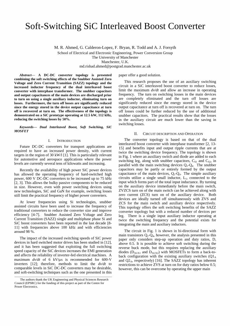
The converter topology is based on that of the dual interleaved boost converter with interphase transformer [2, 13-15] and benefits input and output ripple currents that are at twice the switching device frequency. The topology is shown in Fig. 1 where an auxiliary switch and diode are added to each switching leg, along with snubber capacitors, CS1 and CS2, in parallel with the main switching devices Q1-Q4. The snubber capacitors may be partly or entirely formed by the output capacitance of the main devices, Q1-Q4. The simple auxiliary circuits utilize a single small inductor, L1, connected to the input which forms part of the total input inductance. By turning on the auxiliary device immediately before the main switch, ZVZCS turn on of the main switch can be achieved along with zero current (ZCS) turn on of the auxiliary device. Both devices are ideally turned off simultaneously with ZVS and ZCS for the main switch and auxiliary device respectively. This topology offers the soft switching benefits of the SAZZ converter topology but with a reduced number of devices per leg. There is a single input auxiliary inductor operating at twice the switching frequency and the potential exists for integrating the main and auxiliary inductors.
The circuit in Fig. 1 is shown in bi-directional form with main transistors Q1-Q4, however, the analysis presented in this paper only considers step-up operation and duty ratios, D, above 0.5. It is possible to achieve soft switching during the reverse buck mode, but this requires replacing the auxiliary diodes (DAUX1 and DAUX2) with MOSFETs to form a back-to-back configuration with the existing auxiliary switches (Q1A and Q2A, respectively) [16]. The SAZZ topology has inherent restrictions to achieve ZVS at turn on for duty ratios below 0.5; however, this can be overcome by operating the upper main
The authors thank the UK Engineering and Physical Sciences Research
Council (EPSRC) for the funding of this project as part of the Centre for
Power Electronics.
switches, Q3 and Q4, in a synchronous rectification mode as
shown in [16].
III. CIRCUIT ANALYSIS AND DESIGN
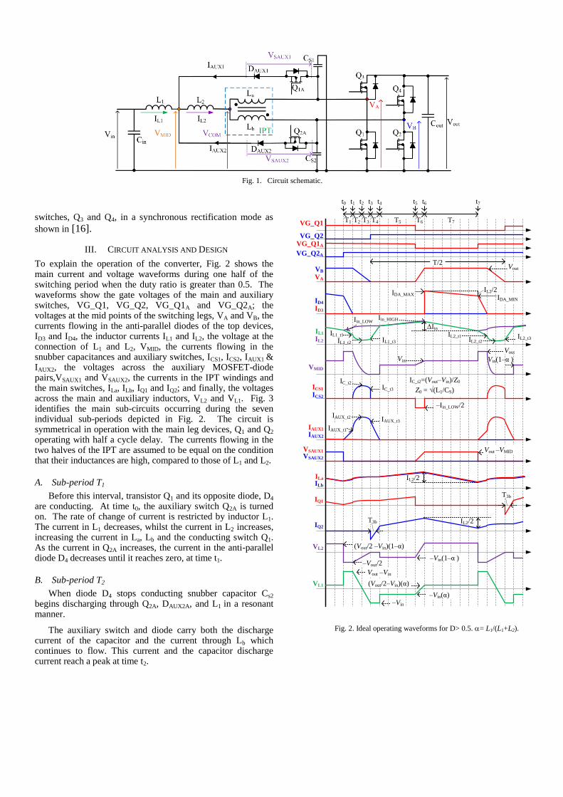
To explain the operation of the converter, Fig. 2 shows the main current and voltage waveforms during one half of the switching period when the duty ratio is greater than 0.5. The waveforms show the gate voltages of the main and auxiliary switches, VG_Q1, VG_Q2, VG_Q1A and VG_Q2A; the voltages at the mid points of the switching legs, VA and VB, the currents flowing in the anti-parallel diodes of the top devices, ID3 and ID4, the inductor currents IL1 and IL2, the voltage at the connection of L1 and L2, VMID, the currents flowing in the snubber capacitances and auxiliary switches, ICS1, ICS2, IAUX1 & IAUX2, the voltages across the auxiliary MOSFET-diode pairs,VSAUX1 and VSAUX2, the currents in the IPT windings and the main switches, ILa, ILb, IQ1 and IQ2; and finally, the voltages across the main and auxiliary inductors, VL2 and VL1. Fig. 3 identifies the main sub-circuits occurring during the seven individual sub-periods depicted in Fig. 2. The circuit is symmetrical in operation with the main leg devices, Q1 and Q2 operating with half a cycle delay. The currents flowing in the two halves of the IPT are assumed to be equal on the condition that their inductances are high, compared to those of L1 and L2.
A. Sub-period T1
Before this interval, transistor Q1 and its opposite diode, D4 are conducting. At time t0, the auxiliary switch Q2A is turned on. The rate of change of current is restricted by inductor L1. The current in L1 decreases, whilst the current in L2 increases, increasing the current in La, Lb and the conducting switch Q1. As the current in Q2A increases, the current in the anti-parallel diode D4 decreases until it reaches zero, at time t1.
B. Sub-period T2
When diode D4 stops conducting snubber capacitor Cs2 begins discharging through Q2A, DAUX2A, and L1 in a resonant manner.
The auxiliary switch and diode carry both the discharge current of the capacitor and the current through Lb which continues to flow. This current and the capacitor discharge current reach a peak at time t2.
Vin(1–α )
VG_Q1
VG_Q1A
VG_Q2
VG_Q2A
VB
VA
ID4
ID3
IL2
IL1
VMID
ICS2
ICS1
IAUX2
IAUX1
VSAUX2
VSAUX1
ILb
ILa
IQ1
IQ2
t0 t1 t2 t4 t6 t7t5
T1 T2 T3 T4 T6
Vin
IC_t2=(Vout–Vin)/Z0
Z0 = √(L1/CS)
VL2
VL1
(Vout/2 –Vin)(1–α)
–Vin(α)
–Vout/2–Vin(1–α )
–Vin
Vout –Vin
(Vout/2–Vin)(α)
IL2/2
t3
IL2/2
Vout
IDA_MIN
IL2_t1
Iin_HIGH
Vout
IC_t3
IAUX_t2
IAUX_t1
IAUX_t3
–Iin_LOW/2
Vout –VMID
T/2
IL2/2IDA_MAX
IL2_t3IL1_t3IL1_t2
IL1_t1
T7T5
Iin_LOW
ΔIin
IL2_t2
IC_t2
T3b
T3b
Fig. 2. Ideal operating waveforms for D> 0.5. = L1/(L1+L2).
Fig. 1. Circuit schematic.
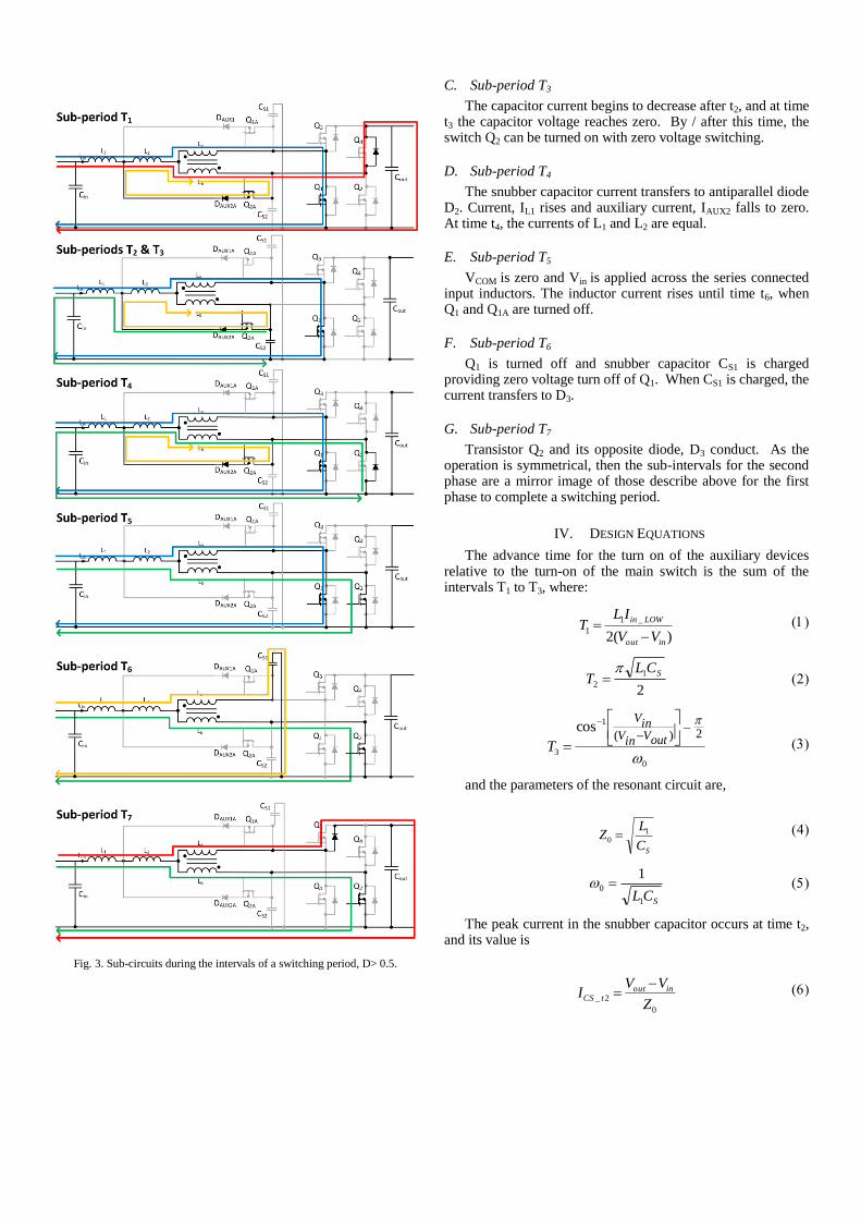
Fig. 3. Sub-circuits during the intervals of a switching period, D> 0.5.
C. Sub-period T3
The capacitor current begins to decrease after t2, and at time t3 the capacitor voltage reaches zero. By / after this time, the switch Q2 can be turned on with zero voltage switching.
D. Sub-period T4
The snubber capacitor current transfers to antiparallel diode D2. Current, IL1 rises and auxiliary current, IAUX2 falls to zero. At time t4, the currents of L1 and L2 are equal.
E. Sub-period T5
VCOM is zero and Vin is applied across the series connected input inductors. The inductor current rises until time t6, when Q1 and Q1A are turned off.
F. Sub-period T6
Q1 is turned off and snubber capacitor CS1 is charged providing zero voltage turn off of Q1. When CS1 is charged, the current transfers to D3.
G. Sub-period T7
Transistor Q2 and its opposite diode, D3 conduct. As the operation is symmetrical, then the sub-intervals for the second phase are a mirror image of those describe above for the first phase to complete a switching period.
IV. DESIGN EQUATIONS
The advance time for the turn on of the auxiliary devices relative to the turn-on of the main switch is the sum of the intervals T1 to T3, where:
)(2
_1
1
inout
LOWin
VV
ILT
2
1
2
SCLT
0
1
3
2)(cos
outVinVinV
T
and the parameters of the resonant circuit are,
SC
LZ 1
0
SCL1
0
1
The peak current in the snubber capacitor occurs at time t2, and its value is
0
2_Z
VVI inout
tCS
Whilst the peak current in the auxiliary switch and diode at t2 is
2_
_
2_2
tCS
LOWin
tAUX II
I
The voltage rating of the auxiliary switch is lower than that of the main leg switches,
VQAUX= Vout –Vin (8)
V. PRACTICAL IMPLEMENTATION– ADVANCE TIME
Turning on the main switches at the exact instants where the voltage across the snubber capacitor reaches zero, t3, would be impractical and difficult to achieve due to the time scales involved in the transients, time delays in logic and gate driver circuitry and unnecessary added complexity to the controller. The best solution to keep a simple control and achieve soft switching is to turn on the auxiliary switches by a fixed period before the main switches.
The advance time should ensure that the snubber capacitor is fully-discharged to avoid turn-on losses; however, when the turn-on transient of the main switch is delayed after t3 there is a period, T3b, where the devices can be turned on to achieve the ZVS, as depicted in the transistor current waveforms IQ1 and IQ2 in Fig. 2.
During the sub-period T3b, the snubber capacitor remains discharged until the current in the auxiliary circuit reaches zero. If the main switch is not turned on in the interval of T3b, then the capacitor will recharge.
The time T3b is given by (9),
in
tCS
bV
ILT
3_
13
where,
3202_3_ sin TTII tCStCS
T3b is therefore dependent only on the input voltage, output voltage and the sizes of L1 and the snubber capacitor. These parameters are not load-dependent when operating the continuous conduction mode and therefore they can be predefined during converter design.
VI. PROTOTYPE DESCRIPTION
A 12.5 kW forced air cooled demonstrator has been constructed to boost the input voltage from 100 V to 400 V.
The main converter leg devices are CREE half-bridge CAS100H12AM1 SiC modules. Each auxiliary circuit is formed by a CREE diode, C4D40120D, and a SiC MOSFET, C2M0080120D.
The 1 nF output capacitance of the CREE modules is used to form the snubber capacitors [17]. The inductors L1 and L2 are foil wound ferrites, with values of 1 µH and 12 µH, respectively. The interphase transformer is also ferrite core based with a stranded enamelled wire winding. The differential inductance was of 0.8 mH.
The converter peak current mode control is implemented using an UCC28220 PWM controller, the main switch PWM signals are delayed at turn on by a fixed delay determined by an analogue delay circuit.
Both gate drivers for the SiC module and the auxiliary SiC MOSFET used Murata MGJ2D152005SC isolated 2 W dual output DC-DC converters for generating 20 V/–5 V gate pulses. TEXAS INSTRUMENTS high speed gate driver UCC27531 was used in series with ZETEX high speed gate drivers (ZXGD3004E6) for driving each MOSFET.
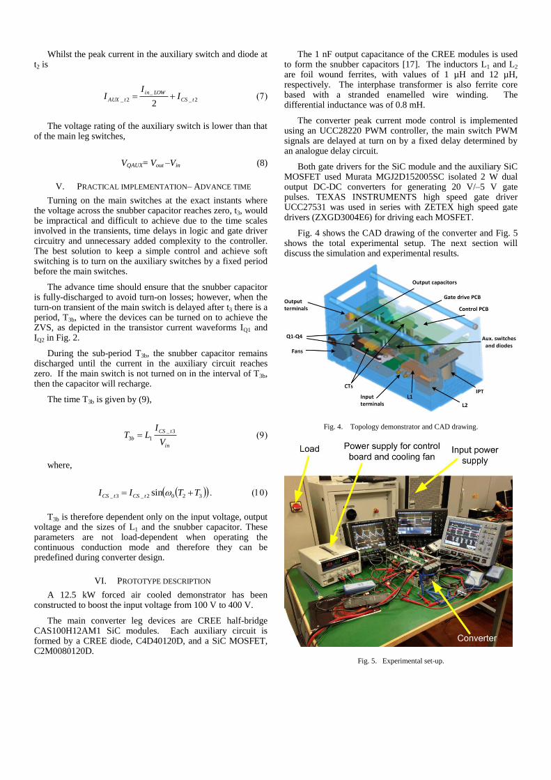
Fig. 4 shows the CAD drawing of the converter and Fig. 5 shows the total experimental setup. The next section will discuss the simulation and experimental results.
Fig. 4. Topology demonstrator and CAD drawing.
Fig. 5. Experimental set-up.
VII. PROTOTYPE RESULTS ANALYSIS
A. Simulation Results
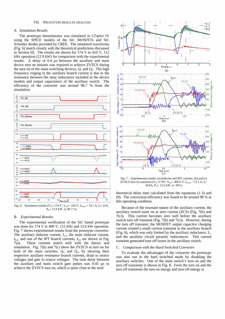
The prototype demonstrator was simulated in LTspice IV using the SPICE models of the SiC MOSFETs and SiC Schottky diodes provided by CREE. The simulated waveforms (Fig. 6) match closely with the theoretical predictions discussed in Section III. The results are shown for 174 V to 410 V, 112 kHz operation (12.9 kW) for comparison with the experimental results. A delay of 0.4 µs between the auxiliary and main device turn on instants was required to achieve ZVZCS during the turn on of the main switching devices, Q1 and Q2. The high frequency ringing in the auxiliary branch current is due to the resonance between the stray inductance included in the device models and output capacitance of the auxiliary switch. The efficiency of the converter was around 98.7 % from the simulation.
The experimental verification of the SiC based prototype was done for 174 V to 400 V, 112 kHz and 12.6 kW operation. Fig. 7 shows experimental results from the prototype converter. The auxiliary inductor current, IL1, the main inductor current, IL2, and one of the IPT branch currents, ILb are shown in Fig. 7(a). These currents match well with the theory and simulation. Fig. 7(b) and 7(c) show the ZVZCS at turn on for both of the main switches, Q1 and Q2, by showing their respective auxiliary resonance branch currents, drain to source voltages and gate to source voltages. The time delay between the auxiliary and main switch gate pulses was 0.45 µs to achieve the ZVZCS turn on, which is quite close to the total
(a)
Fig. 7. Experimental results: (a) Inductor and IPT currents, (b) and (c)
ZVZCS turn on transients (Vin=174V, Vout= 400.6 V, Iinavg = 72.3 A, Io= 30.8A, Pin= 12.6 kW, η= 98%)
theoretical delay time calculated from the equations (1-3) and (9). The conversion efficiency was found to be around 98 % at this operating condition.
Because of the resonant nature of the auxiliary current, the auxiliary switch turns on at zero current (ZCS) (Fig. 7(b) and 7(c)). This current becomes zero well before the auxiliary switch turn off transient (Fig. 7(b) and 7(c)). However, during the turn off transient, the MOSFET output capacitor charging current created a small current transient in the auxiliary branch (Fig. 6), which was only limited by the auxiliary inductance, L1 and the auxiliary circuit parasitic inductances. This current transient generated turn off losses in the auxiliary switch.
C. Comparison with the Hard Switched Converter
To evaluate the advantages of the converter the prototype was also run in the hard switched mode by disabling the auxiliary switches. One of the main switch’s turn on and the turn off transients is shown in Fig. 8. From the turn on and the turn off transients the turn on energy and turn off energy is
Fig. 8. Hard switched results: (a) Turn on transient and (b) Turn off transient
calculated to be 0.4 mJ and 0.18 mJ, respectively. Therefore, for the 112 kHz operation turn on and turn off power losses are in total 90 W and 40 W, respectively. The reduction in switching losses in the soft switching converter is estimated to be 0.4 mJ per device due to the elimination of the turn on losses plus ½ CossVout
2= 0.08 mJ due to the recovery of the
energy stored in the device output capacitance at turn off, giving an overall reduction of switching related power loss of 108 W.
Another improvement in the soft switching topology is the reduction of dv/dt at the turn on transient. This is likely to reduce the EMC and parasitic ringing associated with the rapid switching of SiC MOSFETs. From Fig 7(b) and 7(c), the turn on dv/dt is 3.3 kV/µs at the fastest part of the switching transient. In hard switching, this dv/dt is found to be doubled to 6.6 kV/µs (Fig. 8(a)).
D. Loss breakdown
To analyze further the effectiveness of the proposed topology a loss breakdown was undertaken. Table I shows the component losses at the rated condition (174 V to 400 V, 112 kHz and 12.6 kW) based on the experimental results. Datasheet parameters such as MOSFET on resistances (Rds_on), gate charge (Qg), MOSFET anti-parallel diode on-state voltages (Vsd), Schottky diode on-state voltages (Vf), and magnetic core losses were used to formulate the loss breakdown [17-20].
MOSFET and diode losses were calculated based on the experimental wave-shapes. Magnetic component copper losses were measured using an impedance analyzer. It is clear from the table that the auxiliary circuit is responsible for 38.5 W loss which is around 16 % of the total loss. However, as 108 W switching loss is eliminated compared to the hard switched operation, this soft switching topology still provides an efficiency advantage (around 0.5%) over the hard switching operation.
The calculated efficiency at the rated power is 98.1 %, and in the experimental measurements, an efficiency of 98 % was obtained based on input-output power measurements. At lower output powers, the measured efficiencies were all above 97 %.
TABLE I. LOSS BREAKDOWN OF THE PROTOTYPE CONVERTER (174 V
TO 400 V, 112 KHZ AND 12.6 KW OPERATION)
Loss factors Related
parameter
values
Calculated loss
based on the
experiments
(W)
Main circuit Q1 and Q2 on state Rds_on=14 mΩ 23.6
Q1 and Q2 switching Fsw= 112 kHz 22.4
Q3 and Q4 on state Vsd= 1.35V 66.2
L2 copper RL2 = 1.8 mΩ 9.4
L2 core 10
IPT copper RIPT = 17 mΩ 22
IPT core 18
Q1 and Q2 gate drive Qg =490 nC 2.7
Cooling fan loss (W) 23
Total main circuit loss (W) 197
Auxiliary circuit Q1A and Q2A on state Rds_on= 90 mΩ 8.8
Q1A and Q2A switching Fsw= 112 kHz 2
Q1A and Q2A gate drive Qg =49.2 nC 0.2
DAUX1 and DAUX2 on state Vf= 1.3 V 18.2
L1 copper RL1= 1.8 mΩ 8.3
L1 core 1
Total auxiliary circuit loss(W) 38.5
Total loss (W) 236
Calculated efficiency 98.1 %
VIII. CONCLUSION
A converter topology has been presented which combines the soft switching operation of the SAZZ converter with the increased inductor frequency of the dual interleaved converter. Analytical waveforms and relevant equations have been presented along with the results of a 12.5 kW prototype operating in boost mode from 174 V to 400 V.
The results of hard and soft switching tests show that the additional auxiliary components contribute an extra loss of 38.5 W at the 12.6 kW test point, however the switching losses are reduced from 130 W to 22.4 W. This represents a reduction in the overall converter losses from 293.5 W to 236 W. The efficiency of the prototype at 12.6 kW was measured to be approximately 98 %.
The major advantage of the topology is the significant reduction in dv/dt at the turn on transient of about 50 %, without compromising the efficiency of the converter. The switching losses and dv/dt at turn off of the main devices could be further reduced by the use of additional snubber capacitors, and the potential exists to integrate the auxiliary and main inductors, thereby reducing the component count.
The results confirm the viability of soft switching techniques for SiC converters and suggest that there is significant potential for further increases in switching frequencies.
ACKNOWLEDGMENT
The authors thank Dr. Ian Hawkins for his help in the design of the gate drivers.
REFERENCES
[1] M. Johnson. (2013, 21/05/14). EPSRC Centre for Power Electronics. Delivering strategic value to the UK. EPSRC Centre for Power Electronics opening. Available: http://www.nmi.org.uk/assets/files/ networks/iPower3/Presentations/9 EPSRC Centre ipower nov13.pdf
[2] G. Calderon-Lopez, A. J. Forsyth, D. L. Gordon, and J. R. McIntosh, "Evaluation of SiC BJTs for High-Power DC-DC Converters," IEEE Transactions on Power Electronics, vol. 29, pp. 2474-2481, 2014.
[3] G. Calderon-Lopez and A. J. Forsyth, "High power density DC-DC converter with SiC MOSFETs for electric vehicles," 7th IET International Conference on Power Electronics, Machines and Drives (PEMD 2014) Manchester, UK 2014.
[4] E. Sanchis-Kilders, A. Ferreres, E. Maset, J. D. Ejea, V. Esteve, J. Jordan, R. Garcia, and A. Garrigos, "High Power Passive Soft Switched Interleaved Boost Converters," 35th Annual IEEE Power Electronics Specialists Conference, Aachen, Germany, 2004, pp. 426-432.
[5] J. H. Zhang, J. S. Lai, R. Y. Kim, and W. S. Yu, "High-power density design of a soft-switching high-power bidirectional dc-dc converter," IEEE Transactions on Power Electronics, vol. 22, pp. 1145-1153, Jul 2007.
[6] G. Calderon-Lopez and A. J. Forsyth, "High-Power Dual-Interleaved ZVS Boost Converter with Interphase Transformer for Electric Vehicles," Applied Power Electronics Conference and Exposition, APEC 2009, Washington DC, USA, 2009, pp. 1-6.
[7] W. Li and X. He, "ZVT Interleaved boost converters for high-efficiency, high step-up DC-DC conversion," Electric Power Applications, IET Proceedings-, vol. 1, pp. 284-290, March 2007.
[8] Y. Tsuruta and A. Kawamura, "Zero voltage switched chopper with SiC-MOSFETs," Energy Conversion Congress and Exposition (ECCE), 2013.
[9] M. Pavlovsky, Y. Tsuruta, and A. Kawamura, "Pursuing high power-density and high efficiency in DC-DC converters for automotive application," IEEE Power Electronics Specialists Conference (PESC), 2008.
[10] Y. Tsuruta, M. Pavlovsky, G. Guidi, and A. Kawamura, "Four quadrant SAZZ-1 chopper for EV and HEV power train," IEEE 8th International Conference on Power Electronics and ECCE Asia (ICPE & ECCE), 2011.
[11] Y. Tsuruta, M. Pavlovsky, and A. Kawamura, "Conditions Limiting the Formation of the ZVZCT Switching in SAZZ Converter," Industry Applications Conference, 2007. 42nd IAS Annual Meeting. Conference Record of the 2007 IEEE, 2007.
[12] N. Oswald, P. Anthony, N. McNeill, and B. H. Stark, "An Experimental Investigation of the Tradeoff between Switching Losses and EMI Generation With Hard-Switched All-Si, Si-SiC, and All-SiC Device Combinations," IEEE Transactions on Power Electronics, vol. 29, pp. 2393-2407, 2014.
[13] F. J. Bryan and A. J. Forsyth, "A power dense DC-DC converter for a small electric vehicle," in Power Electronics, Machines and Drives (PEMD 2012), 6th IET International Conference on, 2012, pp. 1-6.
[14] A. J. Forsyth and G. Calderon-Lopez, "Sampled-Data Analysis of the Dual-Interleaved Boost Converter With Interphase Transformer," IEEE Transactions on Power Electronics, vol. 27, pp. 1338-1346, 2012.
[15] M. Hirakawa, Y. Watanabe, M. Nagano, K. Andoh, S. Nakatomi, S. Hashino, and T. Shimizu, "High power DC/DC converter using extreme close-coupled inductors aimed for electric vehicles," in Power Electronics Conference (IPEC), 2010 International, 2010, pp. 2941-2948.
[16] M. Pavlovsky, G. Guidi, and A. Kawamura, "Buck/Boost DC–DC Converter Topology With Soft Switching in the Whole Operating Region," IEEE Transactions on Power Electronics, vol. 29, pp. 851-862, Feb. 2014.