Michael L. Steigerwald,*,† Luis Echegoyen,*,‡ Colin Nuckolls,*,§,† and Thomas J. Sisto*,†
†Department of Chemistry, Columbia University, New York, New York 10027, United States‡Department of Chemistry, University of Texas at El Paso, El Paso, Texas 79968, United States§The State Key Laboratory of Refractories and Metallurgy, Institute of Advanced Materials and Nanotechnology, School of Chemistryand Chemical Engineering, Wuhan University of Science and Technology, Wuhan 430081, China
*S Supporting Information
ABSTRACT: This Communication details the implemen-tation of a new concept for the design of high-performanceoptoelectronic materials: three-dimensional (3D) gra-phene nanostructures. This general strategy is showcasedthrough the synthesis of a three-bladed propellernanostructure resulting from the coupling and fusion ofa central triptycene hub and helical graphene nanoribbons.Importantly, these 3D graphene nanostructures showremarkable new properties that are distinct from thesubstituent parts. For example, the larger nanostructuresshow an enhancement in absorption and decreased contactresistance in optoelectronic devices. To show theseenhanced properties in a device setting, the nanostructureswere utilized as the electron-extracting layers in perovskitesolar cells. The largest of these nanostructures achieved aPCE of 18.0%, which is one of the highest values reportedfor non-fullerene electron-extracting layers.
In this Communication, we implement a new concept forcreating high-performance optoelectronic materials: three-
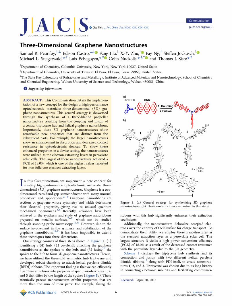
dimensional (3D) graphene nanostructures. Graphene is a two-dimensional zero-band-gap semiconductor with many unusualproperties1 and applications.2−4 Graphene nanoribbons aresections of graphene whose symmetry and width determinestheir electrical properties, giving rise to unusual quantummechanical phenomena.5,6 Recently, advances have beenachieved in the synthesis and study of graphene nanoribbonsprepared on metallic surfaces,7−11 which can be studiedthrough scanning probe microscopy.12,13 However, due to thesurface involvement in the synthesis and stabilization of thegraphene nanoribbons,14,15 it has been impossible to extendthese techniques into three dimensions.Our strategy consists of three steps shown in Figure 1a: (1)
identifying a 3D hub, (2) covalently attaching the graphenenanoribbons as the spokes to the hub, and (3) fusing16 thespokes to the hub to form 3D graphene nanostructures. Herein,we have utilized the three-fold symmetric hub triptycene anddeveloped robust chemistry to attach helical perylene diimide(hPDI) ribbons. The important finding is that we can efficientlyfuse these structures into propeller shaped nanostructures 1, 2,and 3 that differ by the length of the spokes (Figure 1b). Theseatomically precise nanostructures exhibit properties that aremore than the sum of their parts. For example, fusing the
ribbons with this hub significantly enhances their extinctioncoefficients.Additionally, the nanostructures delocalize accepted elec-
trons over the entirety of their surface for charge transport. Todemonstrate their utility, we employ these nanostructures asthe electron extraction layer in a perovskite solar cell. Thelargest structure 3 yields a high power conversion efficiency(PCE) of 18.0% as a result of the decreased contact resistancewith the perovskite layer due to the 3D geometry.Scheme 1 displays the triptycene hub synthesis and its
connection and fusion with two different helical perylenediimide ribbons,17 along with PDI itself, to create nanostruc-tures 1, 2, and 3. Triptycene was chosen due to its long historyin connecting electronic subunits and facilitating communica-
Received: April 20, 2018
Figure 1. (a) General strategy for synthesizing 3D graphenenanostructures. (b) Three nanostructures synthesized in this study.
Communication
pubs.acs.org/JACSCite This: J. Am. Chem. Soc. XXXX, XXX, XXX−XXX
tion between them.18,19 Compound 1 had been previouslyprepared.20 The hub is a tris-borylated triptycene (4), whichhas been previously reported through a multiple stepprocedure.21,22 We found a facile one step synthesis fromtriptycene using iridium-based C−H activation23 in a yield of36%. This reaction produces 4 as a 3:1 mixture of trans and cisregioisomers (see Supporting Information (SI)). In thesubsequent fusion, this mixture is of no consequence becauseall regioisomers converge to the same product. The borylatedtriptycene 4 is coupled to PDI-Br, hPDI2-Br, or hPDI3-Br,then subsequently fused through a visible light flow reaction inquantitative yield to generate nanostructure 1, 2, or 3,respectively (Scheme 1). Even the largest of these, 3, has amolecular weight of 6652 Da, a wingspan of nearly 5 nm, andhigh solubility in numerous organic solvents.We investigated the absorption characteristics to elucidate
any emergent properties as a consequence of the 3D structure(Figure 2a). For the nanostructure series, the longestwavelength absorption onsets are 504, 570, and 619 nm fornanostructures 1, 2, and 3, respectively. This translates tooptical gaps of 2.46, 2.18, and 2.00 eV for 1, 2, and 3,respectively. Two features in the spectra stand out: (1) theexceptionally high molar absorptivity of 3 and (2) the sharp
Figure 2. (a) UV/vis spectra of nanostructures 1, 2, and 3. (b) Structures of compounds hPDI3 and b-hPDI3. (c) UV/vis spectra of b-hPDI3 andnanostructure 3, showing the similarity of electronic structure. (d) Truncated UV/vis spectra of 3, hPDI3, and b-hPDI3, comparing the longestwavelength transitions of three times hPDI3, three times b-hPDI3, and nanostructure 3. While the electronic contribution of benzannulationaccounts for some increase in absorption, it is not responsible for all of the enhancement seen in nanostructure 3.
Scheme 1. Synthesis of Nanostructures 1, 2, and 3 byCovalent Attachment of 1-Bromoperylene-3,4,9,10-tetracarboxylic Diimide (PDI-Br), hPDI2-Br, or hPDI3-Brto a Trisborylated Triptycene Hub Followed by Visible-LightPhotocyclization
Journal of the American Chemical Society Communication
absorption edges.24 Nanostructure 3 displays a molarabsorptivity of >100 000 M−1 cm−1 across the entirety of itsspectrum, and its most intense transition reaches an extinctioncoefficient of 635 000 M−1 cm−1 at ∼410 nm.For the larger two nanostructures 2 and 3, the molar
absorptivities are greater than the sum of the three spokes. Atthe longest wavelength absorption, the difference between theextinction coefficient of three hPDI3 ribbons17 (3 × 83 000M−1 cm−1 = 250 000 M−1 cm−1) and that of the nanostructure3 (455 000 M−1 cm−1) is 205 000 M−1 cm−1. This is an increaseof over 80%. Additionally, the total absorption (integrated area)is increased by 46% as compared to three times that of hPDI3(see SI, Figure S2). These enhancements augur well for theincorporation of these materials in optoelectronic devices.16
In comparing hPDI3 to nanostructure 3, it is apparent thatthe benzannulation of each spoke afforded by the triptycenecould be the cause for this increased absorption. To elucidatethe effect of this benzene ring, we examined the electronicstructure of a benzannulated hPDI3 (b-hPDI3) by DFT(Figure 2b) (see SI, Figure S13). A comparison of the predictedUV/vis spectra of hPDI3 and b-hPDI3 shows a transition inthe latter that is absent in the former. We assign this long-wavelength feature to the promotion of an electron from the πorbitals of the new fused six-membered ring to an erstwhileunoccupied π orbital on the hPDI3 core. In comparing b-hPDI3 to nanostructure 3, the predicted electronic structuresand resultant absorption spectra are qualitatively similar.Unexpectedly, the sum of predicted oscillator strengths forthe long-wavelength absorption feature in nanostructure 3 is3.459, and the comparable predicted sum for b-hPDI3 is 2.739(3 × 0.913; see SI, Figure S14). Thus, between electronicallymatched nanostructure 3 and b-hPDI3, the predicted differ-ence in absorption at the longest wavelength feature betweenthree b-hPDI3 units and nanostructure 3 is around 25%. Toexperimentally confirm these predictions, we prepared b-hPDI3, and its absorption spectrum is indeed qualitativelysimilar to that of nanostructure 3 (Figure 2c). Importantly,simple tripling of the absorptivity of this electronically matchedspoke does not account for the increased absorptivity seen in 3;the extinction coefficient at the longest wavelength of 3 is still120 000 M−1 cm−1 more, or 35% increased, as compared tothree times b-hPDI3 (Figure 2d). The fusion of thesenanoribbons into an organized 3D nanostructure is thusresponsible for the increased absorption. A future in-depthstudy will examine the origin of this enhancement to betterelucidate the role of the triptycene architecture.Nanostructures 1, 2, and 3 can accept many electrons within
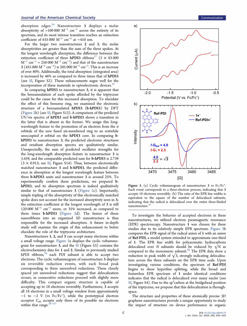
a small voltage range. Figure 3a displays the cyclic voltammo-gram for nanostructure 3, and the SI (Figure S3) contains theelectrochemistry data for 1 and 2. Similar to previously studiedhPDI ribbons,16 each PDI subunit is able to accept twoelectrons. The cyclic voltammogram of nanostructure 3 displayssix reversible reduction events, with each broad peakcorresponding to three unresolved reductions. These closelyspaced yet unresolved reductions suggest that delocalizationoccurs, as consecutive reductions proceed with slightly moredifficulty. This compact organic structure is capable ofaccepting up to 18 electrons reversibly. Furthermore, 3 acceptsall 18 electrons in a small voltage window from approximately−1 to −2 V (vs Fc/Fc+), while the prototypical electronacceptor C60 accepts only three of its possible six electronswithin that range.25−27
To investigate the behavior of accepted electrons in thesenanostructures, we utilized electron paramagnetic resonance(EPR) spectroscopy. Nanostructure 1 was chosen for thesestudies due to its relatively simple EPR spectrum. Figure 3bcompares the EPR signal of the radical anion of 1 with an anionof Ref-PDI, a model system intended to approximate one-thirdof 1. The EPR line width for polyaromatic hydrocarbonsdelocalized over N subunits should be reduced by √N ascompared to the monomeric subunit.28 The EPR data show areduction in peak width of √3, strongly indicating delocaliza-tion across the three subunits on the EPR time scale. Uponinvestigating various conditions, the spectrum of Ref-PDIbegins to show hyperfine splitting, while the broad andfeatureless EPR spectrum of 1 under identical conditionsindicates that the radical is delocalized over many nuclei (seeSI, Figure S4). Due to the sp3carbon at the bridgehead positionof the triptycene, we propose that this delocalization is through-space.The structure and properties of these atomically precise 3D
graphene nanostructures provide a unique opportunity to studythe impact of structure on device performance in organic
Figure 3. (a) Cyclic voltammogram of nanostructure 3 vs Fc/Fc+.Each event corresponds to a three-electron process, indicating that 3accepts 18 electrons reversibly. (b) The ratio of the EPR line widths isequivalent to the square of the number of delocalized subunits,indicating that the radical is delocalized over the entire three-bladednanostructure.28
Journal of the American Chemical Society Communication
electronics. We were interested in studying these compounds asthe electron transport material (ETM) in perovskite solar cellssince fullerenes are known to be effective at electron extractiondue to insertion into the perovskite layer,29,30 which lowers thecontact resistance. We postulated that the morphology of thesenanostructures would facilitate penetration of the spokes intothe perovskite layer (Figure 4a,b).
The nanostructures were compared to phenyl-C61-butyricacid methyl ester (PC61BM), linear hPDI3, and linear b-hPDI3as electron-extracting layers in perovskite solar cells with theconfiguration of ITO/PEDOT:PSS/perovskite/ETM/Ag (Fig-ure 4a). All cells were characterized with a variety of techniquesincluding imaging, X-ray, photovoltaic, electrochemical impe-dance, and time-resolved photophysical measurements (see SI,Figures S5−S9). As shown in Figure 4c, devices based on
nanostructures 2 and 3 show high PCEs of 16.4% and 18.0%,respectively. These values rival the highest reports31 for non-fullerene electron-extracting layers. These PCEs are signifi-cantly higher than the control of PC61BM (15.6%), as well assignificantly higher than the linear ribbons hPDI3 and b-hPDI3(11.0% and 12.0%, respectively).We used space-charge limited current (SCLC)32 measure-
ments to compare electron transport and electrochemicalimpedance spectroscopy (EIS) to probe the interface character-istics of these layers. Devices with the configuration of ITO/Al/ETM/Al were fabricated for PC61BM, linear hPDI3, linear b-hPDI3, 2, and 3 to conduct the SCLC measurements(fabrication details in the SI). Importantly, all layers had anelectron mobility of 10−4 cm2/(V·s), indicating transport is nota factor in the differences in PCE. These results indicate thatthe PCE improvements are from improved interfacial contactand charge transfer between the perovskite and thenanostructures. Indeed, the ohmic resistance of each perovskitesolar cell shows a high-frequency RC arc that is determined bythe contact resistance between the perovskite layer and theETM (Figure 4d).33 The difference in this resistance correlatesdirectly with the PCE. The linear ribbons have the highestresistances and lowest PCEs, followed by PC61BM which showsa significant decrease in resistance due to its known interlayerinsertion34,35 and therefore a significant increase in PCE. The3D graphene nanostructures improve on this trend: 2 showslower resistance and higher PCE than PC61BM, and 3 has theleast resistance and highest PCE of all. We suggest that thelonger arm of nanostructure 3 extends deeper into theperovskite layer (Figure 4b) and increases the surface area forcharge transfer, therefore lowering the resistance further thannanostructure 2.In this Communication we describe the connection and
fusion of graphene nanoribbons to a central hub to yield three-dimensional graphene nanostructures. We synthesize thenanostructures through a new C−H activation protocol totris-functionalize triptycene in one step. The ribbons are thencoupled and fused to the hub with a visible-light, flowphotocyclization to produce atomically defined structures thatare very large (up to molecular weight in excess of 6600), andyet highly soluble. The largest nanostructure exhibits anabsorption increase of over 80% compared to its constituentparts and electrochemically accepts 18 electrons over a 1 Vpotential range. Incorporation into perovskite solar cells as theelectron extraction layer yielded efficiencies of up to 18.0% dueto lower interfacial resistance between the perovskite and thetransport layer. These conclusions underscore the importanceof synthesizing topologically interesting 3D architectures forgraphene nanoribbons and inspire future studies to identifysystems with promising emergent characteristics.
■ ASSOCIATED CONTENT
*S Supporting InformationThe Supporting Information is available free of charge on theACS Publications website at DOI: 10.1021/jacs.8b04119.
Figure 4. (a) Perovskite solar cell configuration. (b) Interlayerpenetration of 3D graphene nanostructures into the perovskite. (c)Distribution of device PCEs. Counts represent individual trials. Curvesindicate normalized distribution for each set of components. Thepercentages indicate average result for each set of devices. (d) Ohmicresistance plot of each component. The interfacial resistance betweenthe perovskite and ETM is assigned to the first, higher-frequency RCarc.
Journal of the American Chemical Society Communication
■ ACKNOWLEDGMENTSC.N. thanks Sheldon and Dorothea Buckler for their generoussupport. Support for this research was provided by the U.S.Office of Naval Research under Award No. N00014-17-1-2205and Award No. N00014-16-1-2921. S.R.P. is supported by theU.S. Department of Defense through the National DefenseScience & Engineering Graduate Fellowship Program. TheColumbia University Shared Materials Characterization Labo-ratory was used extensively for this research. We are grateful toColumbia University for support of this facility. L.E. thanks theU.S. National Science Foundation for generous support underthe NSF-PREM program (DMR 1205302) and CHE-1408865.The Robert A. Welch Foundation is also gratefully acknowl-edged for an endowed chair to L.E. (Grant AH-0033).
■ REFERENCES(1) Nair, R. R.; Blake, P.; Grigorenko, A. N.; Novoselov, K. S.; Booth,T. J.; Stauber, T.; Peres, N. M.; Geim, A. K. Science 2008, 320, 1308.(2) Stankovich, S.; Dikin, D. A.; Dommett, G. H.; Kohlhaas, K. M.;Zimney, E. J.; Stach, E. A.; Piner, R. D.; Nguyen, S. T.; Ruoff, R. S.Nature 2006, 442, 282.(3) Zurutuza, A.; Marinelli, C. Nat. Nanotechnol. 2014, 9, 730.(4) Shahil, K. M.; Balandin, A. A. Solid State Commun. 2012, 152,1331.(5) Zhang, Y.; Tan, Y.-W.; Stormer, H. L.; Kim, P. Nature 2005, 438,201.(6) Ruffieux, P.; Cai, J.; Plumb, N. C.; Patthey, L.; Prezzi, D.; Ferretti,A.; Molinari, E.; Feng, X.; Mullen, K.; Pignedoli, C. A.; Fasel, R. ACSNano 2012, 6, 6930.(7) Chen, Y.-C.; De Oteyza, D. G.; Pedramrazi, Z.; Chen, C.; Fischer,F. R.; Crommie, M. F. ACS Nano 2013, 7, 6123.(8) Bennett, P. B.; Pedramrazi, Z.; Madani, A.; Chen, Y.-C.; deOteyza, D. G.; Chen, C.; Fischer, F. R.; Crommie, M. F.; Bokor, J.Appl. Phys. Lett. 2013, 103, 253114.(9) Chen, Y.-C.; Cao, T.; Chen, C.; Pedramrazi, Z.; Haberer, D.; DeOteyza, D. G.; Fischer, F. R.; Louie, S. G.; Crommie, M. F. Nat.Nanotechnol. 2015, 10, 156.(10) Treier, M.; Pignedoli, C. A.; Laino, T.; Rieger, R.; Mullen, K.;Passerone, D.; Fasel, R. Nat. Chem. 2011, 3, 61.(11) Ruffieux, P.; Wang, S.; Yang, B.; Sanchez-Sanchez, C.; Liu, J.;Dienel, T.; Talirz, L.; Shinde, P.; Pignedoli, C. A.; Passerone, D.; et al.Nature 2016, 531, 489.(12) Zhang, Y.; Tang, T.-T.; Girit, C.; Hao, Z.; Martin, M. C.; Zettl,A.; Crommie, M. F.; Shen, Y. R.; Wang, F. Nature 2009, 459, 820.(13) Zhang, X.; Yazyev, O. V.; Feng, J.; Xie, L.; Tao, C.; Chen, Y.-C.;Jiao, L.; Pedramrazi, Z.; Zettl, A.; Louie, S. G.; et al. ACS Nano 2013,7, 198.
(14) Bhaviripudi, S.; Jia, X.; Dresselhaus, M. S.; Kong, J. Nano Lett.2010, 10, 4128.(15) Simonov, K. A.; Vinogradov, N. A.; Vinogradov, A. S.;Generalov, A. V.; Zagrebina, E. M.; Svirskiy, G. I.; Cafolla, A. A.;Carpy, T.; Cunniffe, J. P.; Taketsugu, T.; Lyalin, A.; Martensson, N.;Preobrajenski, A. B. ACS Nano 2015, 9, 8997.(16) Castro, E.; Sisto, T. J.; Romero, E. L.; Liu, F.; Peurifoy, S. R.;Wang, J.; Zhu, X.; Nuckolls, C.; Echegoyen, L. Angew. Chem., Int. Ed.2017, 56, 14648.(17) Zhong, Y.; Kumar, B.; Oh, S.; Trinh, M. T.; Wu, Y.; Elbert, K.;Li, P.; Zhu, X.; Xiao, S.; Ng, F.; Steigerwald, M. L.; Nuckolls, C. J. Am.Chem. Soc. 2014, 136, 8122.(18) Hayashi, T.; Mataga, N.; Sakata, Y.; Misumi, S. Bull. Chem. Soc.Jpn. 1975, 48, 416.(19) Qi, D.; Zhang, L.; Zhao, L.; Cai, X.; Jiang, J. ChemPhysChem2012, 13, 2046.(20) Meng, D.; Fu, H.; Fan, B.; Zhang, J.; Li, Y.; Sun, Y.; Wang, Z.Chem. - Asian J. 2017, 12, 1286.(21) Zhang, G.; Rominger, F.; Mastalerz, M. Cryst. Growth Des. 2016,16, 5542.(22) Zhang, C.; Chen, C.-F. J. Org. Chem. 2006, 71, 6626.(23) Ishiyama, T.; Takagi, J.; Ishida, K.; Miyaura, N.; Anastasi, N. R.;Hartwig, J. F. J. Am. Chem. Soc. 2002, 124, 390.(24) Zhong, Y.; Sisto, T. J.; Zhang, B.; Miyata, K.; Zhu, X.-Y.;Steigerwald, M. L.; Ng, F.; Nuckolls, C. J. Am. Chem. Soc. 2017, 139,5644.(25) Allemand, P.; Koch, A.; Wudl, F.; Rubin, Y.; Diederich, F.;Alvarez, M.; Anz, S.; Whetten, R. J. Am. Chem. Soc. 1991, 113, 1050.(26) Mirkin, M. V.; Bulhoes, L. O.; Bard, A. J. J. Am. Chem. Soc. 1993,115, 201.(27) Xie, Q.; Perez-Cordero, E.; Echegoyen, L. J. Am. Chem. Soc.1992, 114, 3978.(28) Norris, J. R.; Uphaus, R. A.; Crespi, H. L.; Katz, J. J. Proc. Natl.Acad. Sci. U. S. A. 1971, 68, 625.(29) Castro, E.; Murillo, J.; Fernandez-Delgado, O.; Echegoyen, L. J.Mater. Chem. C 2018, 6, 2635.(30) Fang, Y.; Bi, C.; Wang, D.; Huang, J. ACS Energy Lett. 2017, 2,782.(31) Wu, F.; Gao, W.; Yu, H.; Zhu, L.; Li, L.; Yang, C. J. Mater. Chem.A 2018, 6, 4443.(32) Mihailetchi, V. D.; Wildeman, J.; Blom, P. W. M. Phys. Rev. Lett.2005, 94, 126602.(33) Dualeh, A.; Moehl, T.; Tetreault, N.; Teuscher, J.; Gao, P.;Nazeeruddin, M. K.; Gratzel, M. ACS Nano 2014, 8, 362.(34) Castro, E.; Zavala, G.; Seetharaman, S.; D’Souza, F.; Echegoyen,L. J. Mater. Chem. A 2017, 5, 19485.(35) Tian, C.; Castro, E.; Wang, T.; Betancourt-Solis, G.; Rodriguez,G.; Echegoyen, L. ACS Appl. Mater. Interfaces 2016, 8, 31426.
Journal of the American Chemical Society Communication