Published: July 19, 2011 r2011 American Chemical Society 3413 dx.doi.org/10.1021/nl201823u | Nano Lett. 2011, 11, 3413–3419 LETTER pubs.acs.org/NanoLett Three-Dimensional High-Density Hierarchical Nanowire Architecture for High-Performance Photoelectrochemical Electrodes Jian Shi, † Yukihiro Hara, ‡ Chengliang Sun, † Marc A. Anderson, ‡ and Xudong Wang* ,† † Department of Materials Science and Engineering and ‡ Civil and Environmental Engineering, University of Wisconsin-Madison, Madison, Wisconsin, United States b S Supporting Information P hotocatalyzed water splitting has received considerable at- tention as a clean, abundant and renewable strategy in which to address both the energy crisis and environmental concerns over the use of fossil fuels. 18 Efficient, stable, chemically inert, low-cost, and nontoxic photoelectrochemical (PEC) electrodes are essential to the success of water splitting. 916 Light absorp- tion, charge generation and separation, and the matching of interfacial redox reactions represent the three most fundamental aspects of problems we face in this arena. 1724 A fast interfacial charge transfer rate and suppressed electronhole recombina- tion are greatly desired. 2527 Promising solutions for efficient solar-to-chemical energy conversion include avoiding charge trapping on semiconductor surfaces, increasing semicon- ductor-electrolyte interfacial area, and enhancing the cap- ability for instantaneous charge collection, separation, and transport. 9,12,17,20,28,29 Therefore, three-dimensional (3D) nanowire (NW) networks may represent ideal architectures for high-performance PEC electrodes. High-density treelike branched NW arrays provide a type of architecture that could offer long optical paths for efficient light absorption, high- quality one-dimensional (1D) conducting channels for rapid electronhole separation and charge transport, as well as high surface areas for fast interfacial charge transfer and electrochemical reactions. 4,17 In this paper, we report on the development of a 3D high-density heterogeneous NW architecture by growing titanium dioxide (TiO 2 ) nanorods (NRs) uniformly on dense Si NW array backbones using our surface-reaction-limited pulsed chemical vapor deposition (SPCVD) technique. 30,31 Dramatic increases of photocurrent and photoelectrochemcial efficiency were obtained when the 3D NW architectures were applied as PEC anodes. Fabrication of 3D TiO 2 NR-Si NW architecture is schemati- cally illustrated in Figure 1a. First, vertical Si NW arrays were prepared by selectively etching a heavily doped n-type Si substrate. Second, high density TiO 2 NRs were uniformly grown around the Si NWs via the SPCVD process. Lastly, an additional thin film of anatase TiO 2 was coated on the NR-NW hetero- structure by atomic layer deposition (ALD) to completely cover Si NW surfaces. As schematically shown in Figure 1b, when this heterogeneous structure is used as a PEC anode for water splitting, photocatalyzed H 2 O oxidation reactions would only occur on the TiO 2 surfaces. In principle, the photogenerated electrons should quickly be transported through the Si NW backbone and reach the counter electrode with minimal losses owing to the high conductivity of Si NWs and isolation from electrolyte. 20,28 The very large surface area provided by the TiO 2 NR arrays together with the high-speed electron transport channels provided by the Received: May 29, 2011 Revised: July 10, 2011 ABSTRACT: Three-dimensional (3D) nanowire (NW) net- works are promising for designing high-performance photo- electrochemical (PEC) electrodes owing to their long optical path for efficient light absorption, high-quality one-dimensional conducting channels for rapid electronhole separation and charge transportation, as well as high surface areas for fast interfacial charge transfer and electrochemical reactions. By growing titanium dioxide (TiO 2 ) nanorods (NRs) uniformly on dense Si NW array backbones, we demonstrated a novel three- dimensional high-density heterogeneous NW architecture that could enhance photoelectrochemical efficiency. A 3D NW architecture consisting of 20 μm long wet-etched Si NWs and dense TiO 2 NRs yielded a photoelectrochemical efficiency of 2.1%, which is three times higher than that of TiO 2 film-Si NWs having a coreshell structure. This result suggests that the 3D NW architecture is superior to straight NW arrays for PEC electrode design. The efficiency could be further improved by optimizing the number of overcoating cycles and the length/density of NW backbones. By implementing these 3D NW networks into electrode design, one may be able to advantageously impact PEC and photovoltaic device performance. KEYWORDS: Titanium dioxide, nanorods, 3D nanowire network, photoelectrochemistry, water splitting
Transcript
Published: July 19, 2011
r 2011 American Chemical Society 3413 dx.doi.org/10.1021/nl201823u |Nano Lett. 2011, 11, 3413–3419
LETTER
pubs.acs.org/NanoLett
Three-Dimensional High-Density Hierarchical Nanowire Architecturefor High-Performance Photoelectrochemical ElectrodesJian Shi,† Yukihiro Hara,‡ Chengliang Sun,† Marc A. Anderson,‡ and Xudong Wang*,†
†Department of Materials Science and Engineering and ‡Civil and Environmental Engineering, University of Wisconsin-Madison,Madison, Wisconsin, United States
bS Supporting Information
Photocatalyzed water splitting has received considerable at-tention as a clean, abundant and renewable strategy in which
to address both the energy crisis and environmental concernsover the use of fossil fuels.1�8 Efficient, stable, chemically inert,low-cost, and nontoxic photoelectrochemical (PEC) electrodesare essential to the success of water splitting.9�16 Light absorp-tion, charge generation and separation, and the matching ofinterfacial redox reactions represent the three most fundamentalaspects of problems we face in this arena.17�24 A fast interfacialcharge transfer rate and suppressed electron�hole recombina-tion are greatly desired.25�27 Promising solutions for efficientsolar-to-chemical energy conversion include avoiding chargetrapping on semiconductor surfaces, increasing semicon-ductor-electrolyte interfacial area, and enhancing the cap-ability for instantaneous charge collection, separation, andtransport.9,12,17,20,28,29 Therefore, three-dimensional (3D)nanowire (NW) networks may represent ideal architecturesfor high-performance PEC electrodes. High-density treelikebranched NW arrays provide a type of architecture that couldoffer long optical paths for efficient light absorption, high-quality one-dimensional (1D) conducting channels for rapidelectron�hole separation and charge transport, as well ashigh surface areas for fast interfacial charge transfer andelectrochemical reactions.4,17 In this paper, we report onthe development of a 3D high-density heterogeneous NWarchitecture by growing titanium dioxide (TiO2) nanorods
(NRs) uniformly on dense Si NW array backbones using oursurface-reaction-limited pulsed chemical vapor deposition(SPCVD) technique.30,31 Dramatic increases of photocurrentand photoelectrochemcial efficiency were obtained when the3D NW architectures were applied as PEC anodes.
Fabrication of 3D TiO2 NR-Si NW architecture is schemati-cally illustrated in Figure 1a. First, vertical Si NW arrays wereprepared by selectively etching a heavily doped n-type Sisubstrate. Second, high density TiO2 NRs were uniformly grownaround the Si NWs via the SPCVD process. Lastly, an additionalthin film of anatase TiO2 was coated on the NR-NW hetero-structure by atomic layer deposition (ALD) to completely coverSi NW surfaces. As schematically shown in Figure 1b, when thisheterogeneous structure is used as a PEC anode for water splitting,photocatalyzedH2O oxidation reactions would only occur on theTiO2 surfaces. In principle, the photogenerated electrons shouldquickly be transported through the Si NW backbone and reachthe counter electrode with minimal losses owing to the highconductivity of Si NWs and isolation from electrolyte.20,28 Thevery large surface area provided by the TiO2 NR arrays togetherwith the high-speed electron transport channels provided by the
Received: May 29, 2011Revised: July 10, 2011
ABSTRACT: Three-dimensional (3D) nanowire (NW) net-works are promising for designing high-performance photo-electrochemical (PEC) electrodes owing to their long opticalpath for efficient light absorption, high-quality one-dimensionalconducting channels for rapid electron�hole separation andcharge transportation, as well as high surface areas for fastinterfacial charge transfer and electrochemical reactions. Bygrowing titanium dioxide (TiO2) nanorods (NRs) uniformly ondense Si NW array backbones, we demonstrated a novel three-dimensional high-density heterogeneous NW architecture thatcould enhance photoelectrochemical efficiency. A 3D NWarchitecture consisting of 20 μm long wet-etched Si NWs anddense TiO2NRs yielded a photoelectrochemical efficiency of 2.1%, which is three times higher than that of TiO2 film-Si NWs havinga core�shell structure. This result suggests that the 3DNW architecture is superior to straight NW arrays for PEC electrode design.The efficiency could be further improved by optimizing the number of overcoating cycles and the length/density of NW backbones.By implementing these 3D NW networks into electrode design, one may be able to advantageously impact PEC and photovoltaicdevice performance.
KEYWORDS: Titanium dioxide, nanorods, 3D nanowire network, photoelectrochemistry, water splitting
3414 dx.doi.org/10.1021/nl201823u |Nano Lett. 2011, 11, 3413–3419
Nano Letters LETTER
Si NWs are promising features that could lead to a significantimprovement of photoelectrochemical efficiency.
Driven by this rationale, Si NWbackbones were first fabricatedby deep reactive ion etching (RIE) technique using a self-assembled nanosphere monolayer as mask (the fabrication de-tails are included in Supporting Information).32,33 N-type Siwafer (0.001�0.005Ωcm) was used to fabricate NWs to ensuregood electrical conductivity. The typical size of as-fabricated SiNWs were ∼300 nm in diameter, ∼15 μm long, and ∼200 nmapart from each other (inset of Figure 1a). After 600 cycles ofSPCVD growth (see Supporting Information for experimentaldetails), uniform TiO2 NRs were deposited on the entire Si NWsurface. Figure 2a shows a top-view scanning electron micro-scopy (SEM) image of as-grown TiO2 NRs that illustrate thisfeature. The NRs exhibited uniform dimensions that are 35 (5 nm in diameter and 252 ( 37 nm in length. All the Si NWsremained straight and no agglomeration was observed after TiO2
NR growth (Figure 2b). Figure 2c,d shows SEM images taken atthe middle and bottom regions of the cross-section, respectively,showing a uniform and dense coverage of TiO2 NRs. This is atypical growth result across the entire sample and it providesevidence that a very large quantity of uniform-sized TiO2 NRscan be grown on all possible surfaces despite the extremelynarrow and deep spaces left in between Si NWs.
Consistent with our previous research, the as-deposited TiO2
NRs exhibited pure anatase phase character as identified byX-ray diffraction (XRD) (Supporting Information Figure S1). Allthe NRs were single crystals rooted on the surface of Si NWs(Supporting Information Figure S2a). Selective area electrondiffraction (SAED) (Supporting Information Figure S2b) furtherconfirmed that the single-crystalline anatase structure andgrowth/surface arrangements were identical to the TiO2 NRsgrown in anodic aluminum oxide (AAO) templates.30 This obser-vation suggests that the supporting surfaces/substrates havenegligible influence on the crystal structure and orientations ofTiO2 NRs.
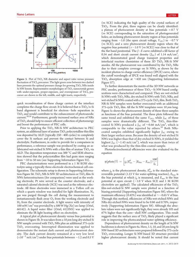
As we reported previously, the growth of TiO2 NRs wasdictated by surface adsorption and reactions in which the partialpressure of TiCl4 precursor played an important role. Specifi-cally, when the partial pressure of TiCl4 was too high, surplussupply of precursor diminishes the difference of adsorption andsurface chemical reaction rates on different crystal facets of TiO2,thereby rendering an isotropic nanoparticle growth. When theprecursor supply was reduced to an appropriate level, the growthrate of the TiO2 (001) plane became distinctly faster and thus the
crystal growth transformed to an anisotropic mode and NRmorphology was received. This growth behavior observed inAAO channels also applies to the Si NW matrix. To bettergeneralize these growth patterns, here we use pressure change(ΔP) upon 500ms precursor pulsing (500 ms is the fixed pulsingtime and ΔP is the pressure difference of chamber before andafter ALD valve is on) to describe the morphology-precursorsupply relationship. Nine different ΔP of TiCl4 precursor wereexamined ranging from 20 to 1000 millitorr, while all the othergrowth parameters remained constant (500 ms pulsing time, 600SPCVD cycles, and 600 �C).Here,ΔPwas adjusted by regulatingthe temperature of TiCl4 precursor. Figure 3 illustrates thechange of morphology in TiO2 NRs as a function of ΔP ofTiCl4. When the ΔP was as low as 20 millitorr, TiO2 NRs couldnot fully evolve and both the diameter and aspect ratio of theNRswere small (left inset of Figure 3). When ΔP was above ∼160millitorr, large crystallites were obtained indicating a superfluoussupply of precursors (right inset of Figure 3). The appropriateΔP was found between 60 to 140 millitorr as indicated by thelight green zone in Figure 3. In this region, aspect ratio as high as9 was achieved when the ΔP was 120 millitorr (central inset ofFigure3), demonstrating the ideal conditions forTiO2NRsgrowing ina high-density Si NW forest.
Dry-etched Si NWs offered a good template in which to studythe growth behavior of TiO2 NRs on Si surfaces. However, theirfabrication procedures are relatively complicated and costly. Inorder to further apply this technique to applicable PEC electrodedesign on a large scale, wet-etched Si NW arrays were used forgrowing these NRs. In this case, Si NWswere fabricated using thesame heavily doped Si wafer by the metal-assisted wet-etchingtechnique (see Supporting Information for experimental details).20
This technique can produce vertical Si NW arrays with higherdensity, smaller size, and a larger aspect ratio compared to the dry-etching technique (Supporting Information Figure S3). However,one should caution that assemblages or bundles of NW tips alwaysexist due to the capillary force from etchant solution.
Under the optimized SPCVD condition (ΔPwas 120 millitorrwith 500 ms pulsing time), high-density TiO2 NRs havinguniform dimensions were successfully deposited on the wet-etched Si NWs. Figure 4a is a planar view of a wet-etched Si NWforest after the growth of these NRs. Tip bundling can be clearlyobserved. Closer examination showed that the Si NWs were verythin and exhibited irregular cross sections as highlighted byyellow dashed circles in the inset of Figure 4a. While the openspaces left within the bundling area were very small, the TiO2
Figure 1. (a) Schematic procedures for making treelike TiO2 NR-Si NW 3D architectures. (b) Schematic illustration of using TiO2 NR-Si NWheterostructure as PEC anode for water splitting reactions.
3415 dx.doi.org/10.1021/nl201823u |Nano Lett. 2011, 11, 3413–3419
Nano Letters LETTER
NRs could be found filling all these spaces. These TiO2 NRs are30 ( 6 nm in diameter and 243 ( 31 nm in length statistically.Figure 4b shows that the Si NWs were∼25 μm in length, wherethe top portions (a few μm long) were bundled together. Belowthe bundles, Si NWs are evenly distributed providing a goodtemplate for conformal NRs growth. Higher-magnification SEMimages acquired along the length direction of the Si NWs forestconfirmed the dense and uniform coverage of theseNRs. Figure 4c,dare two representative images indicating the density and dimen-sions of TiO2 NRs were nearly identical at the middle and bottomregions. The NRs grew out laterally from the Si NWs and filledout the interspaces. Thus, considerably large surface area andhigh porosity were created by such a 3D architecture.
Undoped TiO2 by vapor deposition usually appears n-typesemiconductor due to intrinsic defects such as O vacancies and/or
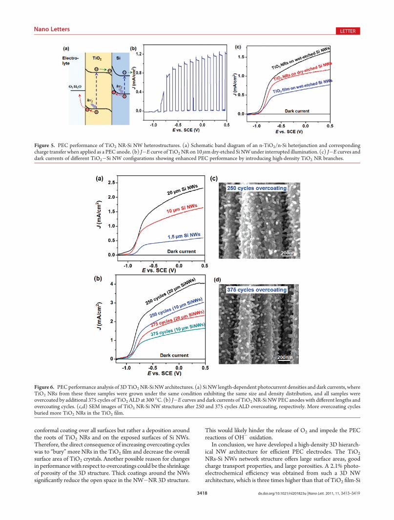
Ti interstitials.34,35 When in contact with n-type Si, the bandstructure of TiO2 will likely be reconfigured. The predictedequilibrium band alignment is schematically shown in Figure 5a.An electron accumulation region and a hole accumulation regionare expected to appear on theTiO2 and Si sides of the interface.
20,28
Upon illumination, electron�hole pairs can be generated in bothTiO2 and Si. The TiO2 NRs or polycrystalline films only absorblight below 420 nm (Supporting Information Figure S4). Thus,most visible light is still available for Si to absorb. Preferable bandbending between TiO2 and electrolyte directs photogeneratedholes in TiO2 toward the TiO2/electrolyte interface that in turnoxidize OH� ions in solution into O2. Meanwhile, photogeneratedelectrons in Si flow to the counter electrode for H2O reduction.The charge accumulation regions at the TiO2/Si interface attractphotogenerated electrons from TiO2 and holes from Si. Thus,
Figure 2. TiO2 NRs grown on vertical Si NW arrays fabricated by dry etching. (a) Top view of Si NWs uniformly covered with high-density TiO2 NRsthat grew laterally out of the side surfaces. Inset is an SEM image of the Si NWs fabricated by deep RIE using nanosphere monolayer as amask. (b) Cross-section of TiO2 NRs-coated Si NW arrays, where the lengths of Si NWs were∼15 μm. (c,d) The middle and bottom portions of Si NWs showing denseand uniform coating of TiO2 NRs along the entire NW length.
3416 dx.doi.org/10.1021/nl201823u |Nano Lett. 2011, 11, 3413–3419
Nano Letters LETTER
quick recombination of these charge carriers at the interfacecompletes the charge flow circuit. It is believed that n-TiO2/n-Siband alignment is beneficial for electron�hole separation inTiO2 and would contribute to the enhancement of photoanodiccurrent.20,28 Furthermore, greatly increased surface area of NRsof TiO2 should help to ensure efficient collection of photoenergyand boost the performance of PEC cells.
Prior to applying the TiO2 NR-Si NW architecture to PECsystem, an additional layer of anatase TiO2 polycrystalline thin filmwas deposited by ALD (typically 250�400 cycles) to completelycover the Si surfaces and prevent the contact between Si andelectrolyte. Furthermore, in order to provide for a comparison inperformance, a reference sample was produced by coating an as-fabricated wet-etched Si NWs with a thin film of anatase TiO2 viaALD. The deposition temperature was 300 �C and SEM observa-tion showed that the polycrystalline film had grain sizes rangingfrom ∼10 to 50 nm (see Supporting Information Figure S5).
PEC characterizations were performed in a 1 M KOH elec-trolyte using a typically three-electrode electrochemical cell con-figuration. The schematic setup is shown in Supporting Informa-tion Figure S6. TiO2 NR-Si NW 3D architectures or TiO2 film-SiNWs heterostructures (for comparison) were used as the work-ing electrode; Pt wire served as the counter electrode; and asaturated calomel electrode (SCE) was used as the reference elec-trode. All three electrodes were immersed in a Teflon cell onwhich a quartz window was installed for light illumination. N2
gas was purged through the cell during the measurement toinstantaneously flush away O2 from the working electrode andH2 from the counter electrode. A light source with intensity of100 mW/cm2 was provided by a 500WHg (Xe) arc lamp (Oriel,66142). A liquid water filter (Oriel, 6123NS) was applied toeliminate the IR light heating effect on electrolyte.
A typical plot of photocurrent density versus bias potential isshown in Figure 5b. It was taken from a 10 μm long dry-etched SiNW sample covered with TiO2 NRs plus an additional 375-cycleTiO2 overcoating. Interrupted illumination was applied todemonstrate the instant dark current and photocurrent den-sity. The dark current density remained at a very low level(<10�2 mA/cm2) under bias potentials between�1.2 and 0.5 V
(vs SCE) indicating the high quality of the crystal surfaces ofTiO2. From the plot, three regions can be clearly identified:a plateau of photocurrent density at bias potentials >-0.7 V(vs SCE) corresponding to the saturation of photogeneratedholes; an inclining photocurrent density region at bias potentialsranging from �1.0 (the open circuit voltage, VOC) to �0.7 V(vs SCE); and a zero photocurrent density region where thenegative bias potential (<�1.0 V (vs SCE)) was close to that ofthe flat band penitential. The J�E curve exhibited a fill factor of0.54 and short circuit current density (JSC) of 1.14 mA/cm2,which demonstrated good charge transport properties andinterfacial reaction chemistries of these 3D TiO2 NR-Si NWanodes. All the photocurrent was contributed by the TiO2 NRsdue to their complete coverage on Si NWs, as shown by theincident photon to charge carrier efficiency (IPCE) curve, wherethe cutoff wavelength of IPCE was found well aligned with theTiO2 absorption edge at ∼420 nm (Supporting InformationFigure S7).
To further demonstrate the merits of the 3D NW networks asPEC anodes, performance of three TiO2�Si NW-based config-urations were characterized and compared. They are wet-etchedSi NWs with TiO2 NRs, dry-etched Si NWs with TiO2 NRs, andwet-etched Si NWs coated with a 375-cycle TiO2 film. Both TiO2
NR-Si NW samples were further overcoated with an additional375-cycle TiO2 film. All the Si NW templates were 10 μm long.Figure 5c shows the photocurrent density of these three samplesas functions of the bias potential. The three plots followed thesame trend and exhibited the same VOC, while JSC of thesesamples were dramatically different. The TiO2 thin-film-coated Si NWs produced a JSC of ∼0.66 mA/cm2, which iscomparable to the value reported by others.20 Both NRs-coated samples exhibited significantly higher JSC owing totheir larger surface areas. Because the density of wet-etched SiNWs was higher than that of dry-etched Si NWs, it yielded thehighest JSC (∼1.43 mA/cm2), which was more than twice ofwhat was produced by the thin-film-coated sample.
Photoelectrochemical efficiencies were also evaluated via theequation
ηðphotoÞ% ¼ jpðE0rev � jEbias � EaocjÞ100I0
� �
where jp is the photocurrent density, Erev0 is the standard state-
reversible potential (1.23 V for water-splitting reaction), Ebias isthe bias potential at which jp is measured, and Eaoc is the biaspotential at open circuit (�1.0 V when SCE and 1 M KOHelectrolyte are applied). The calculated efficiencies of the TiO2
film-wet-etched-Si NW sample were plotted as a function ofbiasing potential (Supporting Information Figure S8), where themaximum efficiency (0.42%) was identified at∼�0.65 V of bias.Through this method, efficiencies of NRs-wet-etched-NWs andNRs-dry-etched-NWs were found to be 0.86 and 0.70%, respec-tively (Supporting Information Figure S8). Although the abso-lute values were not significantly high, they were already 105 and67% higher than the core�shell NW configuration. This resultsuggests that the surface area of TiO2 likely played a significantrole in improving the photocatalyzed water splitting efficiency.
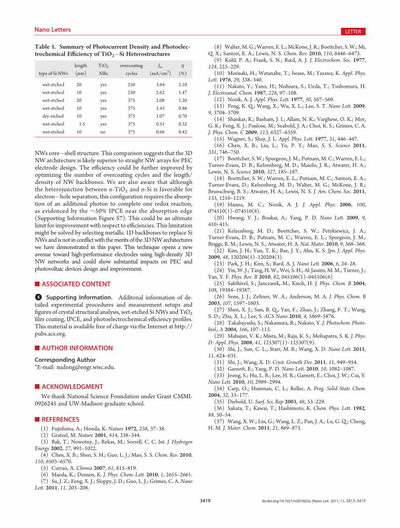
Dependence of photocurrent density on the length of Si NWbackbones is shown in Figure 6a. Here, 1.5, 10, and 20 μm long SiNW-based 3D architectures were prepared followed by 375-cycleTiO2 overcoating. Longer Si NW-based 3D structure providedhigher photocurrent density. It should be noted that current
Figure 3. Plot of TiO2 NR diameter and aspect ratio versus pressurefluctuation of TiCl4 precursor. The light green zone between two dashedlines presents the optimal pressure change for growing TiO2 NRs insideSi NW forests. Representative morphologies of TiO2 nanocrystals grownwith under-exposure, proper-exposure, and overexposure of TiCl4 pre-cursor are shown in the left, middle, and right insets, respectively.
3417 dx.doi.org/10.1021/nl201823u |Nano Lett. 2011, 11, 3413–3419
Nano Letters LETTER
density per unit length of 10 and 20 μm Si NWs was lowerthan that of the 1.5 μm sample, although the size and densitydistribution of the TiO2 NRs was nearly identical. This nonlinearincrease of photocurrent is possibly related to the difficulty ofremoving O2 from deep inside the 3D NW forest. Efficiencycalculations showed that the 20 μm sample had a three timeshigher efficiency than the 1.5μmone suggesting the performanceenhancement resulted from an increase of surface area (Table 1).
TiO2 overcoating was a necessary treatment in order to isolateSi from the electrolyte and achieve a stable PEC anode. However,one should caution that the overcoating thickness might alsoalter PEC performance. To demonstrate the overcoating influ-ence, 250 and 375 ALD cycles of overcoating were applied toTiO2 NRs-covered wet-etched Si NW arrays with two differentlengths (10 and 20 μm). Figure 6b illustrates the corresponding
J�E curves of these four different samples. The sample condi-tions, JSC, and efficiencies (derived from Supporting InformationFigure S8) are also summarized in Table 1. It was found that thesample with the 250-cycle overcoating produced higher photo-current than the ones with a 375-cycle of overcoating. The highestefficiency (2.1%) was identified from the 20 μm sample with the250-cycle overcoating. This is a competitive value as compared toother TiO2-based PEC anodes.4,10,14,20,22,23,25,26,28,29,36,37
In order to provide a visual interpretation for these perfor-mance changes, the morphology of the overcoatings was inves-tigated by SEM. As shown in Figure 6c,d, diameters of the TiO2
NRs were nearly unaffected after overcoating. However, theobservable lengths of the NRs were clearly shortened when theovercoating cycles increased from 250 to 375 (Figure 6c, d). Thisobservation suggests that the 300 �CTiO2 ALD did not provide a
Figure 4. TiO2 NRs grown on vertical Si NW arrays fabricated by wet etching. (a) Top view of Si NWs after TiO2 NR growth. Bundling of NW tips wasdue to capillary attraction during wet etching. Inset is a higher-magnification SEM image showing TiO2NRs growing laterally around Si NWs. (b) Cross-section of vertical Si NW arrays covered with TiO2 NRs. The Si NWs are ∼25 μm long and the top ∼5 μm region was bundled together. (c,d) Themiddle and bottom portions of Si NWs showing dense and uniform coverage of TiO2 NRs along the entire NW length.
3418 dx.doi.org/10.1021/nl201823u |Nano Lett. 2011, 11, 3413–3419
Nano Letters LETTER
conformal coating over all surfaces but rather a deposition aroundthe roots of TiO2 NRs and on the exposed surfaces of Si NWs.Therefore, the direct consequence of increasing overcoating cycleswas to “bury”more NRs in the TiO2 film and decrease the overallsurface area of TiO2 crystals. Another possible reason for changesin performancewith respect to overcoatings could be the shrinkageof porosity of the 3D structure. Thick coatings around the NWssignificantly reduce the open space in the NW�NR 3D structure.
This would likely hinder the release of O2 and impede the PECreactions of OH� oxidation.
In conclusion, we have developed a high-density 3D hierarch-ical NW architecture for efficient PEC electrodes. The TiO2
NRs-Si NWs network structure offers large surface areas, goodcharge transport properties, and large porosities. A 2.1% photo-electrochemical efficiency was obtained from such a 3D NWarchitecture, which is three times higher than that of TiO2 film-Si
Figure 6. PECperformance analysis of 3DTiO2NR-Si NWarchitectures. (a) Si NW length-dependent photocurrent densities and dark currents, whereTiO2 NRs from these three samples were grown under the same condition exhibiting the same size and density distribution, and all samples wereovercoated by additional 375 cycles of TiO2 ALD at 300 �C. (b) J�E curves and dark currents of TiO2NR-Si NWPEC anodes with different lengths andovercoating cycles. (c,d) SEM images of TiO2 NR-Si NW structures after 250 and 375 cycles ALD overcoating, respectively. More overcoating cyclesburied more TiO2 NRs in the TiO2 film.
Figure 5. PEC performance of TiO2 NR-Si NW heterostructures. (a) Schematic band diagram of an n-TiO2/n-Si heterjunction and correspondingcharge transfer when applied as a PEC anode. (b) J�E curve of TiO2NRon 10μmdry-etched Si NWunder interrupted illumination. (c) J�E curves anddark currents of different TiO2�Si NW configurations showing enhanced PEC performance by introducing high-density TiO2 NR branches.
3419 dx.doi.org/10.1021/nl201823u |Nano Lett. 2011, 11, 3413–3419
Nano Letters LETTER
NWs core�shell structure. This comparison suggests that the 3DNW architecture is likely superior to straight NW arrays for PECelectrode design. The efficiency could be further improved byoptimizing the number of overcoating cycles and the length/density of NW backbones. We are also aware that althoughthe heterojunction between n-TiO2 and n-Si is favorable forelectron�hole separation, this configuration requires the absorp-tion of an additional photon to complete one redox reaction,as evidenced by the ∼50% IPCE near the absorption edge(Supporting Information Figure S7). This could be an ultimatelimit for improvement with respect to efficiencies. This limitationmight be solved by selecting metallic 1D backbones to replace SiNWs and is not in conflictwith themerits of the 3DNWarchitectureswe have demonstrated in this paper. This technique opens a newavenue toward high-performance electrodes using high-density 3DNW networks and could show substantial impacts on PEC andphotovoltaic devices design and improvement.
’ASSOCIATED CONTENT
bS Supporting Information. Additonal information of de-tailed experimental procedures and measurement setups andfigures of crystal structural analysis, wet-etched Si NWs and TiO2
film coating, IPCE, and photoelectrochemical efficiency profiles.This material is available free of charge via the Internet at http://pubs.acs.org.
We thank National Science Foundation under Grant CMMI-0926245 and UW-Madison graduate school.
’REFERENCES
(1) Fujishima, A.; Honda, K. Nature 1972, 238, 37–38.(2) Gratzel, M. Nature 2001, 414, 338–344.(3) Bak, T.; Nowotny, J.; Rekas, M.; Sorrell, C. C. Int. J. Hydrogen
Energy 2002, 27, 991–1022.(4) Chen, X. B.; Shen, S. H.; Guo, L. J.; Mao, S. S. Chem. Rev. 2010,
110, 6503–6570.(5) Currao, A. Chimia 2007, 61, 815–819.(6) Maeda, K.; Domen, K. J. Phys. Chem. Lett. 2010, 1, 2655–2661.(7) Su, J. Z.; Feng, X. J.; Sloppy, J. D.; Guo, L. J.; Grimes, C. A.Nano
Lett. 2011, 11, 203–208.
(8) Walter,M. G.;Warren, E. L.;McKone, J. R.; Boettcher, S.W.;Mi,Q. X.; Santori, E. A.; Lewis, N. S. Chem. Rev. 2010, 110, 6446–6473.
(9) Kohl, P. A.; Frank, S. N.; Bard, A. J. J. Electrochem. Soc. 1977,124, 225–229.
(10) Morisaki, H.; Watanabe, T.; Iwase, M.; Yazawa, K. Appl. Phys.Lett. 1976, 29, 338–340.
(12) Nozik, A. J. Appl. Phys. Lett. 1977, 30, 567–569.(13) Peng, K. Q.; Wang, X.; Wu, X. L.; Lee, S. T. Nano Lett. 2009,
9, 3704–3709.(14) Shankar, K.; Basham, J. I.; Allam, N. K.; Varghese, O. K.; Mor,
G. K.; Feng, X. J.; Paulose, M.; Seabold, J. A.; Choi, K. S.; Grimes, C. A.J. Phys. Chem. C 2009, 113, 6327–6359.
(15) Wagner, S.; Shay, J. L. Appl. Phys. Lett. 1977, 31, 446–447.(16) Chen, X. B.; Liu, L.; Yu, P. Y.; Mao, S. S. Science 2011,
331, 746–750.(17) Boettcher, S.W.; Spurgeon, J.M.; Putnam,M. C.;Warren, E. L.;
Turner-Evans, D. B.; Kelzenberg, M. D.; Maiolo, J. R.; Atwater, H. A.;Lewis, N. S. Science 2010, 327, 185–187.
(18) Boettcher, S. W.; Warren, E. L.; Putnam, M. C.; Santori, E. A.;Turner-Evans, D.; Kelzenberg, M. D.; Walter, M. G.; McKone, J. R.;Brunschwig, B. S.; Atwater, H. A.; Lewis, N. S. J. Am. Chem. Soc. 2011,133, 1216–1219.
(19) Hanna, M. C.; Nozik, A. J. J. Appl. Phys. 2006, 100,074510(1)–074510(8).
(20) Hwang, Y. J.; Boukai, A.; Yang, P. D. Nano Lett. 2009, 9,410–415.
(21) Kelzenberg, M. D.; Boettcher, S. W.; Petykiewicz, J. A.;Turner-Evans, D. B.; Putnam, M. C.; Warren, E. L.; Spurgeon, J. M.;Briggs, R. M.; Lewis, N. S.; Atwater, H. A.Nat. Mater. 2010, 9, 368–368.
(22) Kim, J. H.; Yun, T. K.; Bae, J. Y.; Ahn, K. S. Jpn. J. Appl. Phys.2009, 48, 120204(1)–120204(3).
(23) Park, J. H.; Kim, S.; Bard, A. J. Nano Lett. 2006, 6, 24–28.(24) Yin, W. J.; Tang, H.W.; Wei, S. H.; Al-Jassim, M. M.; Turner, J.;
Yan, Y. F. Phys. Rev. B 2010, 82, 045106(1)–045106(6).(25) Sakthivel, S.; Janczarek, M.; Kisch, H. J. Phys. Chem. B 2004,
108, 19384–19387.(26) Sene, J. J.; Zeltner, W. A.; Anderson, M. A. J. Phys. Chem. B
2003, 107, 1597–1603.(27) Shen, X. J.; Sun, B. Q.; Yan, F.; Zhao, J.; Zhang, F. T.; Wang,
S. D.; Zhu, X. L.; Lee, S. ACS Nano 2010, 4, 5869–5876.(28) Takabayashi, S.; Nakamura, R.; Nakato, Y. J. Photochem. Photo-
biol., A 2004, 166, 107–113.(29) Mahajan, V. K.; Misra, M.; Raja, K. S.; Mohapatra, S. K. J. Phys.
D: Appl. Phys. 2008, 41, 125307(1)–125307(9).(30) Shi, J.; Sun, C. L.; Starr, M. B.; Wang, X. D. Nano Lett. 2011,
11, 624–631.(31) Shi, J.; Wang, X. D. Cryst. Growth Des. 2011, 11, 949–954.(32) Garnett, E.; Yang, P. D. Nano Lett. 2010, 10, 1082–1087.(33) Jeong, S.; Hu, L. B.; Lee, H. R.; Garnett, E.; Choi, J. W.; Cui, Y.
Nano Lett. 2010, 10, 2989–2994.(34) Carp, O.; Huisman, C. L.; Reller, A. Prog. Solid State Chem.
2004, 32, 33–177.(35) Diebold, U. Surf. Sci. Rep 2003, 48, 53–229.(36) Sakata, T.; Kawai, T.; Hashimoto, K. Chem. Phys. Lett. 1982,
88, 50–54.(37) Wang, X. W.; Liu, G.; Wang, L. Z.; Pan, J. A.; Lu, G. Q.; Cheng,
H. M. J. Mater. Chem. 2011, 21, 869–873.
Table 1. Summary of Photocurrent Density and Photoelec-trochemical Efficiency of TiO2�Si Heterostructures