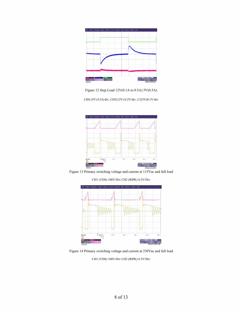
1 of 13 TIDA-00618 8.5W Dual Output (5V/12V) Universal Input AC/DC Isolated Flyback Reference Design with PSR. Primary Side Regulation switcher which provides isolated dual outputs, 5V and 12V rails, with DC stacking of the secondaries to provide output voltage regulation that is equivalent to opto‐coupler based solution. Low system parts count and built in advanced protection features result in a cost‐ effective solution with an average efficiency of nearly 75% at 230V Performance Data and Typical Characteristic Curves: Figure1. 5V Load Regulation 5 5.05 5.1 5.15 5.2 5.25 5.3 5.35 5.4 5.45 5.5 0 100 200 300 400 500 600 5V Output (V) 5V Load Current (mA) Load Regulation 5V Output 115Vac with 12V Load parameter 0mA 50mA 100mA 200mA 300mA 400mA 500mA
Primary Side Regulation switcher which provides isolated dual outputs, 5V and 12V rails, with DC stacking of the secondaries to provide output voltage regulation that is equivalent to opto‐coupler based solution. Low system parts count and built in advanced protection features result in a cost‐effective solution with an average efficiency of nearly 75% at 230V
Performance Data and Typical Characteristic Curves:
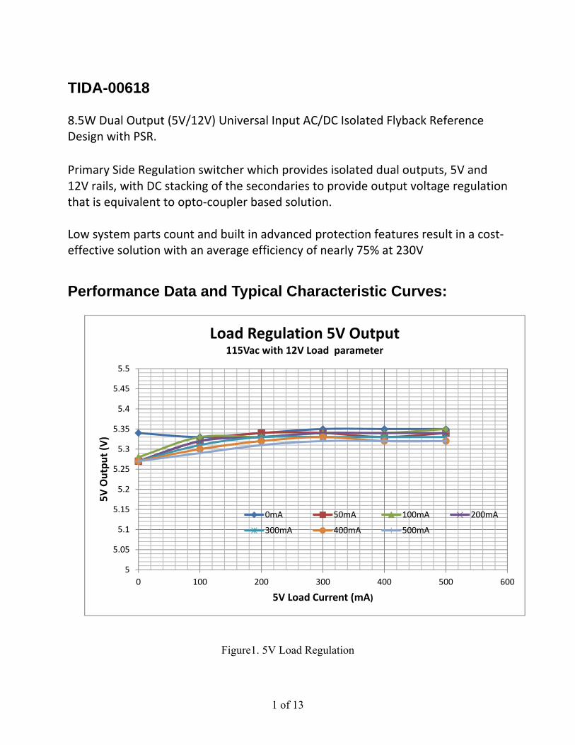
Figure1. 5V Load Regulation
5
5.05
5.1
5.15
5.2
5.25
5.3
5.35
5.4
5.45
5.5
0 100 200 300 400 500 600
5V Output (V)
5V Load Current (mA)
Load Regulation 5V Output 115Vac with 12V Load parameter
0mA 50mA 100mA 200mA
300mA 400mA 500mA
2 of 13
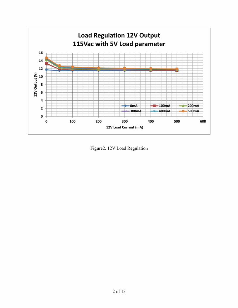
Figure2. 12V Load Regulation
0
2
4
6
8
10
12
14
16
0 100 200 300 400 500 600
12V Output (V)
12V Load Current (mA)
Load Regulation 12V Output115Vac with 5V Load parameter
0mA 100mA 200mA
300mA 400mA 500mA
3 of 13
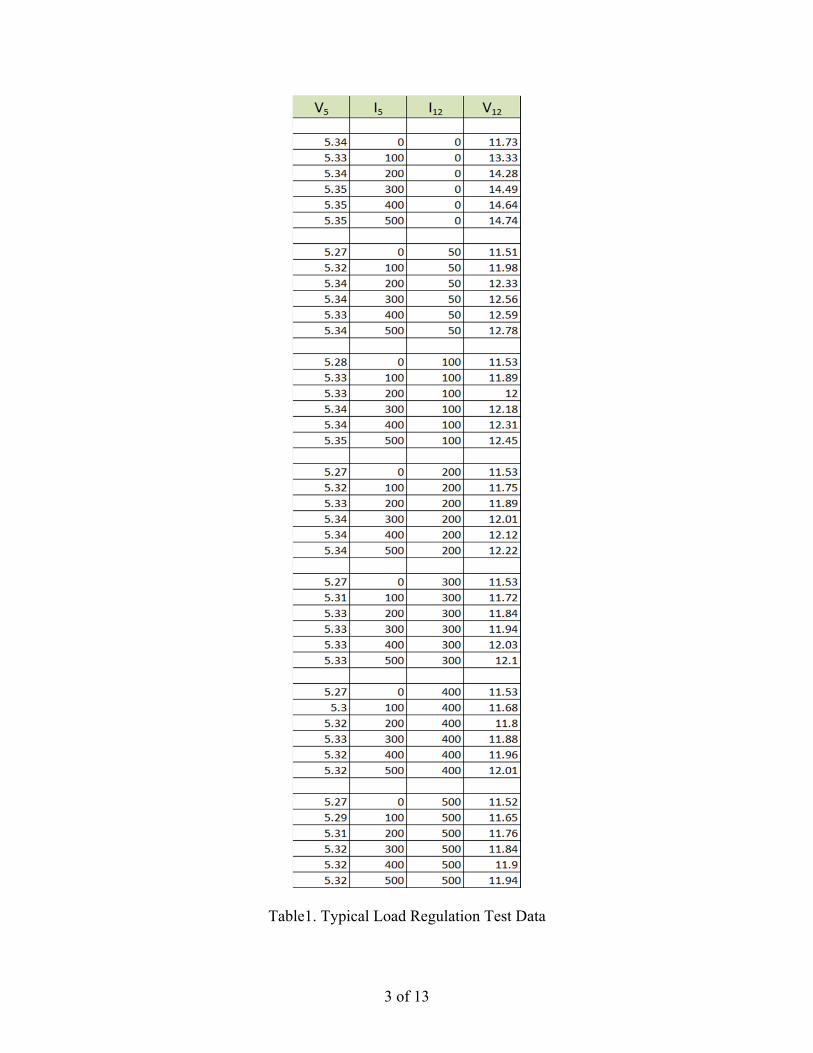
Table1. Typical Load Regulation Test Data
4 of 13
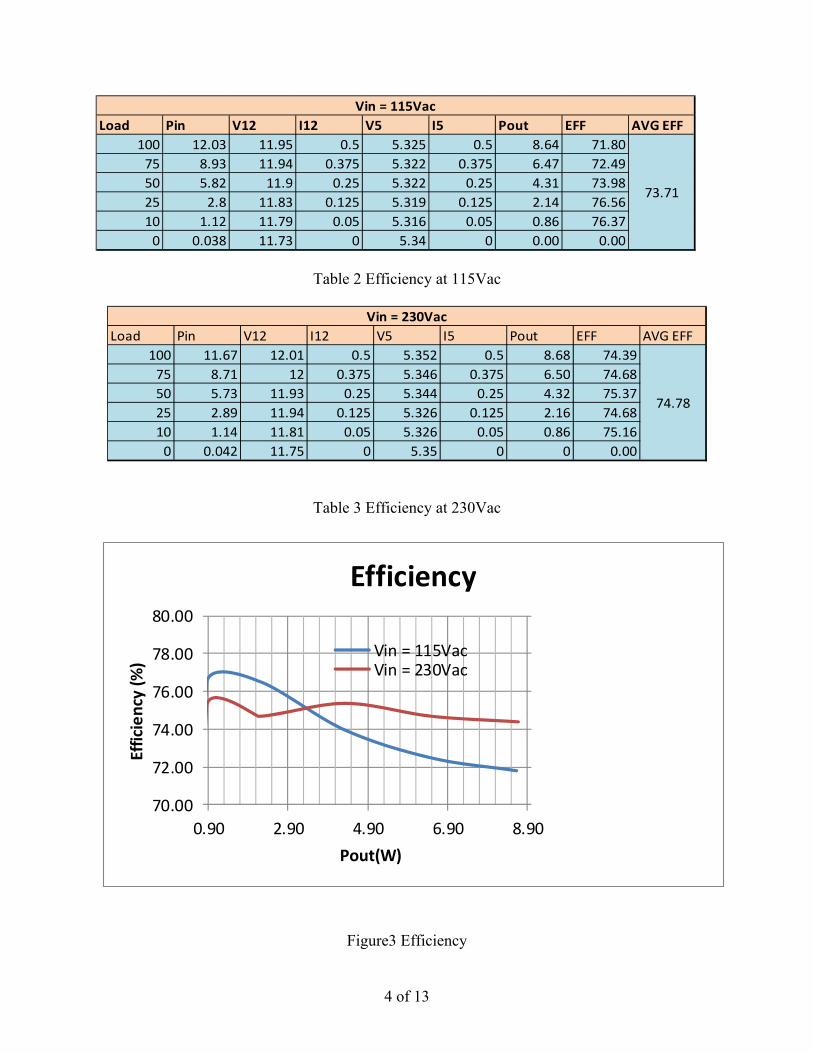
Load Pin V12 I12 V5 I5 Pout EFF AVG EFF
100 12.03 11.95 0.5 5.325 0.5 8.64 71.80
75 8.93 11.94 0.375 5.322 0.375 6.47 72.49
50 5.82 11.9 0.25 5.322 0.25 4.31 73.98
25 2.8 11.83 0.125 5.319 0.125 2.14 76.56
10 1.12 11.79 0.05 5.316 0.05 0.86 76.37
0 0.038 11.73 0 5.34 0 0.00 0.00
73.71
Vin = 115Vac
Table 2 Efficiency at 115Vac
Load Pin V12 I12 V5 I5 Pout EFF AVG EFF
100 11.67 12.01 0.5 5.352 0.5 8.68 74.39
75 8.71 12 0.375 5.346 0.375 6.50 74.68
50 5.73 11.93 0.25 5.344 0.25 4.32 75.37
25 2.89 11.94 0.125 5.326 0.125 2.16 74.68
10 1.14 11.81 0.05 5.326 0.05 0.86 75.16
0 0.042 11.75 0 5.35 0 0 0.00
74.78
Vin = 230Vac
Table 3 Efficiency at 230Vac
70.00
72.00
74.00
76.00
78.00
80.00
0.90 2.90 4.90 6.90 8.90
Efficiency (%)
Pout(W)
Efficiency
Vin = 115VacVin = 230Vac
Figure3 Efficiency
5 of 13
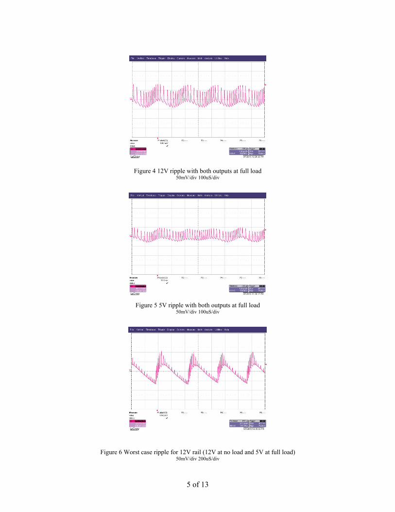
Figure 4 12V ripple with both outputs at full load 50mV/div 100uS/div
Figure 5 5V ripple with both outputs at full load 50mV/div 100uS/div
Figure 6 Worst case ripple for 12V rail (12V at no load and 5V at full load)
50mV/div 200uS/div
6 of 13
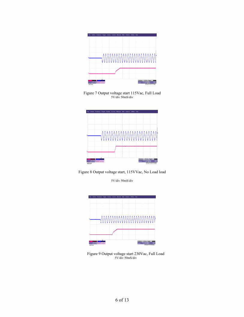
Figure 7 Output voltage start 115Vac, Full Load 5V/div 50mS/div
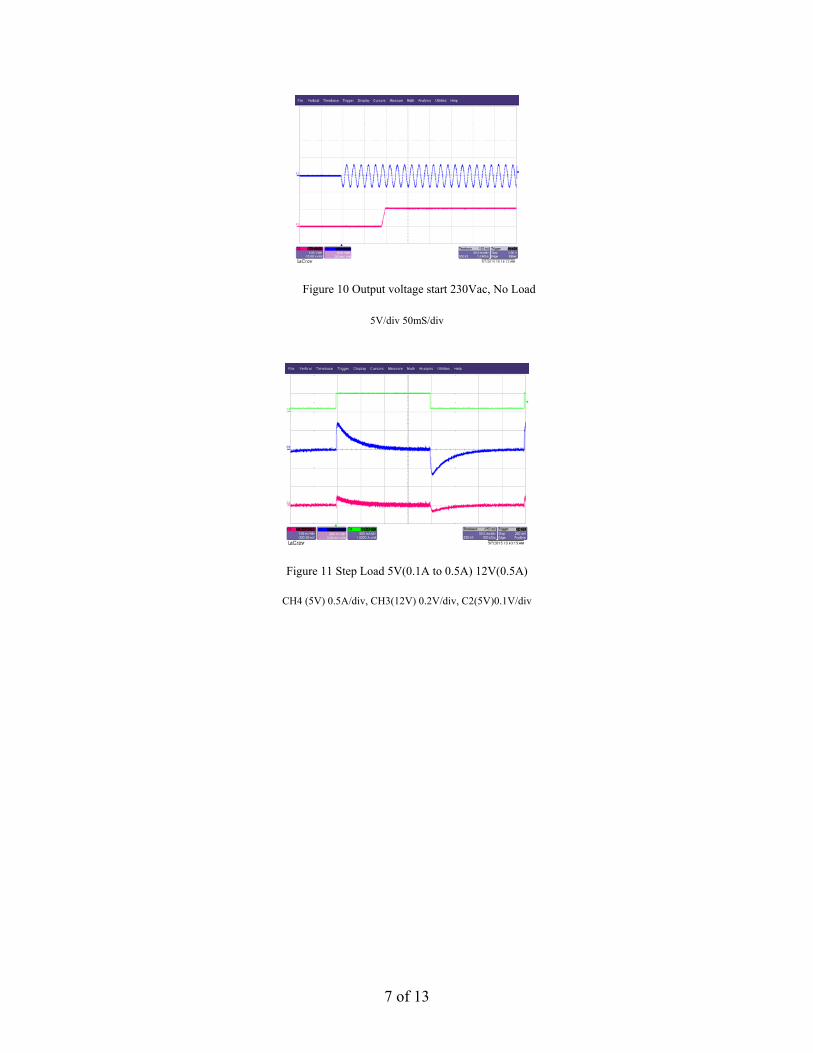
Figure 8 Output voltage start, 115VVac, No Load load
5V/div 50mS/div
Figure 9 Output voltage start 230Vac, Full Load 5V/div 50mS/div
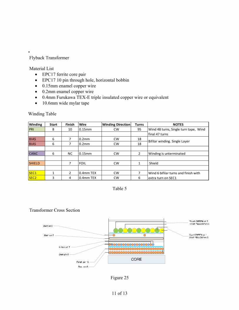
Winding Table Winding Start Finish Wire Winding Direction Turns NOTES
PRI 8 10 0.15mm CW 95
BIAS 6 7 0.2mm CW 18
BIAS 6 7 0.2mm CW 18
CANC 6 NC 0.15mm CW 2 Winding is unterminated
SHIELD 7 FOIL CW 1 Shield
SEC1 1 2 0.4mm TEX CW 7
SEC2 3 4 0.4mm TEX CW 6
Bifilar winding. Single Layer
Wind 48 turns, Single turn tape, Wind
final 47 turns
Wind 6 bifilar turns and finish with
extra turn on SEC1
Table 5
Transformer Cross Section
Figure 25
12 of 13
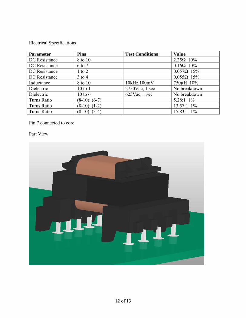
Electrical Specifications Parameter Pins Test Conditions Value DC Resistance 8 to 10 2.25Ω 10% DC Resistance 6 to 7 0.16Ω 10% DC Resistance 1 to 2 0.057Ω 15% DC Resistance 3 to 4 0.055Ω 15% Inductance 8 to 10 10kHz,100mV 750µH 10% Dielectric 10 to 1 2750Vac, 1 sec No breakdown Dielectric 10 to 6 625Vac, 1 sec No breakdown Turns Ratio (8-10): (6-7) 5.28:1 1% Turns Ratio (8-10): (1-2) 13.57:1 1% Turns Ratio (8-10): (3-4) 15.83:1 1% Pin 7 connected to core Part View
13 of 13
IMPORTANT NOTICE FOR TI REFERENCE DESIGNS
Texas Instruments Incorporated ("TI") reference designs are solely intended to assist designers (“Buyers”) who are developing systems thatincorporate TI semiconductor products (also referred to herein as “components”). Buyer understands and agrees that Buyer remainsresponsible for using its independent analysis, evaluation and judgment in designing Buyer’s systems and products.
TI reference designs have been created using standard laboratory conditions and engineering practices. TI has not conducted anytesting other than that specifically described in the published documentation for a particular reference design. TI may makecorrections, enhancements, improvements and other changes to its reference designs.
Buyers are authorized to use TI reference designs with the TI component(s) identified in each particular reference design and to modify thereference design in the development of their end products. HOWEVER, NO OTHER LICENSE, EXPRESS OR IMPLIED, BY ESTOPPELOR OTHERWISE TO ANY OTHER TI INTELLECTUAL PROPERTY RIGHT, AND NO LICENSE TO ANY THIRD PARTY TECHNOLOGYOR INTELLECTUAL PROPERTY RIGHT, IS GRANTED HEREIN, including but not limited to any patent right, copyright, mask work right,or other intellectual property right relating to any combination, machine, or process in which TI components or services are used.Information published by TI regarding third-party products or services does not constitute a license to use such products or services, or awarranty or endorsement thereof. Use of such information may require a license from a third party under the patents or other intellectualproperty of the third party, or a license from TI under the patents or other intellectual property of TI.
TI REFERENCE DESIGNS ARE PROVIDED "AS IS". TI MAKES NO WARRANTIES OR REPRESENTATIONS WITH REGARD TO THEREFERENCE DESIGNS OR USE OF THE REFERENCE DESIGNS, EXPRESS, IMPLIED OR STATUTORY, INCLUDING ACCURACY ORCOMPLETENESS. TI DISCLAIMS ANY WARRANTY OF TITLE AND ANY IMPLIED WARRANTIES OF MERCHANTABILITY, FITNESSFOR A PARTICULAR PURPOSE, QUIET ENJOYMENT, QUIET POSSESSION, AND NON-INFRINGEMENT OF ANY THIRD PARTYINTELLECTUAL PROPERTY RIGHTS WITH REGARD TO TI REFERENCE DESIGNS OR USE THEREOF. TI SHALL NOT BE LIABLEFOR AND SHALL NOT DEFEND OR INDEMNIFY BUYERS AGAINST ANY THIRD PARTY INFRINGEMENT CLAIM THAT RELATES TOOR IS BASED ON A COMBINATION OF COMPONENTS PROVIDED IN A TI REFERENCE DESIGN. IN NO EVENT SHALL TI BELIABLE FOR ANY ACTUAL, SPECIAL, INCIDENTAL, CONSEQUENTIAL OR INDIRECT DAMAGES, HOWEVER CAUSED, ON ANYTHEORY OF LIABILITY AND WHETHER OR NOT TI HAS BEEN ADVISED OF THE POSSIBILITY OF SUCH DAMAGES, ARISING INANY WAY OUT OF TI REFERENCE DESIGNS OR BUYER’S USE OF TI REFERENCE DESIGNS.
TI reserves the right to make corrections, enhancements, improvements and other changes to its semiconductor products and services perJESD46, latest issue, and to discontinue any product or service per JESD48, latest issue. Buyers should obtain the latest relevantinformation before placing orders and should verify that such information is current and complete. All semiconductor products are soldsubject to TI’s terms and conditions of sale supplied at the time of order acknowledgment.
TI warrants performance of its components to the specifications applicable at the time of sale, in accordance with the warranty in TI’s termsand conditions of sale of semiconductor products. Testing and other quality control techniques for TI components are used to the extent TIdeems necessary to support this warranty. Except where mandated by applicable law, testing of all parameters of each component is notnecessarily performed.
TI assumes no liability for applications assistance or the design of Buyers’ products. Buyers are responsible for their products andapplications using TI components. To minimize the risks associated with Buyers’ products and applications, Buyers should provideadequate design and operating safeguards.
Reproduction of significant portions of TI information in TI data books, data sheets or reference designs is permissible only if reproduction iswithout alteration and is accompanied by all associated warranties, conditions, limitations, and notices. TI is not responsible or liable forsuch altered documentation. Information of third parties may be subject to additional restrictions.
Buyer acknowledges and agrees that it is solely responsible for compliance with all legal, regulatory and safety-related requirementsconcerning its products, and any use of TI components in its applications, notwithstanding any applications-related information or supportthat may be provided by TI. Buyer represents and agrees that it has all the necessary expertise to create and implement safeguards thatanticipate dangerous failures, monitor failures and their consequences, lessen the likelihood of dangerous failures and take appropriateremedial actions. Buyer will fully indemnify TI and its representatives against any damages arising out of the use of any TI components inBuyer’s safety-critical applications.
In some cases, TI components may be promoted specifically to facilitate safety-related applications. With such components, TI’s goal is tohelp enable customers to design and create their own end-product solutions that meet applicable functional safety standards andrequirements. Nonetheless, such components are subject to these terms.
No TI components are authorized for use in FDA Class III (or similar life-critical medical equipment) unless authorized officers of the partieshave executed an agreement specifically governing such use.
Only those TI components that TI has specifically designated as military grade or “enhanced plastic” are designed and intended for use inmilitary/aerospace applications or environments. Buyer acknowledges and agrees that any military or aerospace use of TI components thathave not been so designated is solely at Buyer's risk, and Buyer is solely responsible for compliance with all legal and regulatoryrequirements in connection with such use.
TI has specifically designated certain components as meeting ISO/TS16949 requirements, mainly for automotive use. In any case of use ofnon-designated products, TI will not be responsible for any failure to meet ISO/TS16949.IMPORTANT NOTICE