Date post: | 29-May-2018 |
Category: |
Documents |
Upload: | hoangkhanh |
View: | 225 times |
Download: | 0 times |
Time-Interleaved Continuous-Time Delta-Sigma Modulators
by
Trevor C. Caldwell
A thesis submitted in conformity with the requirements for the degree of Master of Applied Science
Graduate Department of Electrical and Computer Engineering
University of Toronto
© Copyright by Trevor C. Caldwell (2004)
ii
Time-Interleaved Continuous-Time Delta-Sigma Modulators
Trevor C. Caldwell
Degree of Master of Applied Science, 2004
Graduate Department of Electrical and Computer Engineering University of Toronto
Abstract
ABSTRACT In this thesis, a method of time-interleaving continuous-time delta-sigma modulators is
investigated. The derivation of the modulator starting from a discrete-time time-
interleaved structure is presented. With various simplifications, the resulting modulator
has only a single-path of integrators, making it robust to DC offsets. A third-order low-
pass continuous-time time-interleaved delta-sigma modulator with an oversampling ratio
of 5 is designed in a mµ18.0 CMOS technology with a V8.1 supply voltage.
Experimental results show that an SNDR of dB57 and a dynamic range of dB60 are
obtained with a sampling frequency of MHz100 . With a sampling frequency of
MHz200 , an SNDR of dB49 with a dynamic range of dB55 is achieved. The power
consumption is mW101 at MHz100 , and mW103 at MHz200 .
iii
Acknowledgements
ACKNOWLEDGMENTS First I would like to thank my supervisor, Professor David A. Johns, for his insight and
suggestions throughout the course of this project. I appreciate the time and
encouragement he has given me.
I would also like to thank CMC for providing the semiconductor fabrication
service that made the implementation of my design possible. Also, I would like to thank
the National Sciences and Engineering Research Council of Canada (NSERC) for their
financial support throughout my graduate studies.
I would like to thank Navid, Imran, Ahmed, Robert, and the students in BA5000
for their help throughout this project.
Finally, I would like to thank my family and my girlfriend Paula for their
continued support throughout the entire thesis.
iv
Table of Contents
TABLE OF CONTENTS
Abstract.............................................................................................................................. ii
Acknowledgments ............................................................................................................ iii
Table of Contents ............................................................................................................. iv
List of Figures.................................................................................................................. vii
List of Tables .................................................................................................................... ix
Chapter 1 Introduction............................................................................................... 1 1.1 Related Work ........................................................................................................ 3 1.2 Outline .................................................................................................................. 4
Chapter 2 Background Information.......................................................................... 5 2.1 General Delta-Sigma Modulators ......................................................................... 5
2.1.1 Oversampling.................................................................................................. 6 2.1.2 Noise-Shaping ................................................................................................. 7
2.2 Discrete-to-Continuous Transform....................................................................... 8 2.2.1 Basic Transform.............................................................................................. 8 2.2.2 Transform for Return-to-Zero DAC Pulses .................................................. 10
2.3 Time-Interleaved Modulators ............................................................................. 12 2.3.1 Block Digital Filters ..................................................................................... 12 2.3.2 Application to Delta-Sigma Modulators....................................................... 15
2.4 Summary............................................................................................................. 18
Chapter 3 Derivation and Simulations.................................................................... 19 3.1 The Derivation .................................................................................................... 19
3.1.1 Design ........................................................................................................... 19 3.1.2 Discrete-Time Loop Filters........................................................................... 22 3.1.3 Elimination of Downsamplers....................................................................... 22 3.1.4 Continuous-Time Loop Filters...................................................................... 26 3.1.5 Return-to-Zero DAC ..................................................................................... 27 3.1.6 Conversion to Integrators ............................................................................. 29 3.1.7 Input Loop Filters ......................................................................................... 29 3.1.8 Integrator Mismatch ..................................................................................... 30 3.1.9 DC offsets...................................................................................................... 31 3.1.10 Evaluating the Unknowns ............................................................................. 33 3.1.11 Dynamic Range Scaling................................................................................ 34 3.1.12 Signal and Noise Transfer Functions ........................................................... 36
3.2 MATLAB Simulations ....................................................................................... 38 3.2.1 Ideal System .................................................................................................. 39 3.2.2 Finite-Gain Opamps ..................................................................................... 40 3.2.3 Addition of Opamp Poles .............................................................................. 41 3.2.4 Integrator Coefficient Mismatch................................................................... 42
TABLE OF CONTENTS
v
3.2.5 DAC Mismatch.............................................................................................. 43 3.2.6 DAC Path Mismatch ..................................................................................... 44 3.2.7 Comparator Mismatch .................................................................................. 44 3.2.8 Integrator Offsets .......................................................................................... 45 3.2.9 DAC Clock Jitter........................................................................................... 46 3.2.10 All Non-Idealities .......................................................................................... 47
3.3 Summary............................................................................................................. 49
Chapter 4 Circuit Design.......................................................................................... 51 4.1 The Integrators.................................................................................................... 52
4.1.1 Resistor and Capacitor Values ..................................................................... 52 4.1.2 Capacitive Tuning......................................................................................... 53 4.1.3 Operational Amplifier................................................................................... 53 4.1.4 Common-Mode Feedback ............................................................................. 56 4.1.5 Startup Circuit .............................................................................................. 56
4.2 The Digital-to-Analog Converters ...................................................................... 57 4.2.1 General ......................................................................................................... 57 4.2.2 Full-Scale Currents....................................................................................... 58 4.2.3 Sizing............................................................................................................. 59 4.2.4 Return-to-Zero .............................................................................................. 60 4.2.5 Layout Considerations .................................................................................. 61 4.2.6 Seventh DAC ................................................................................................. 63
4.3 The Analog-to-Digital Converters ...................................................................... 63 4.3.1 Preamplifier .................................................................................................. 64 4.3.2 Comparator................................................................................................... 65 4.3.3 Power ............................................................................................................ 66
4.4 The Summer........................................................................................................ 66 4.4.1 Transconductor ............................................................................................. 67 4.4.2 Summer Circuit ............................................................................................. 68
4.5 The Clock Generator........................................................................................... 69 4.5.1 Clock Signals ................................................................................................ 69 4.5.2 Advancing the DAC Clocks........................................................................... 70
4.6 Other Circuits...................................................................................................... 71 4.6.1 Thermometer-to-Binary Decoder.................................................................. 71 4.6.2 Biasing Circuit .............................................................................................. 72 4.6.3 Sample-and-Hold .......................................................................................... 73
4.7 Spice Simulations ............................................................................................... 74 4.8 Summary............................................................................................................. 75
Chapter 5 Experimental Results.............................................................................. 76 5.1 Equipment and Test Setup .................................................................................. 76
5.1.1 Printed Circuit Board ................................................................................... 76 5.1.2 Equipment ..................................................................................................... 77 5.1.3 Test Setup ...................................................................................................... 77
5.2 Measured Results................................................................................................ 78 5.2.1 Output Spectra .............................................................................................. 78 5.2.2 Dynamic Range............................................................................................. 81
TABLE OF CONTENTS
vi
5.2.3 Signal Transfer Function .............................................................................. 83 5.2.4 Two-Tone Test............................................................................................... 83
5.3 Summary............................................................................................................. 84
Chapter 6 Conclusions.............................................................................................. 86 6.1 Future Work........................................................................................................ 86
Appendix A Measurements ..................................................................................... 88 A.1 Signal-to-Noise and Distortion Ratio ................................................................. 88 A.2 Signal-to-Noise Ratio ......................................................................................... 89 A.3 Spurious-Free Dynamic Range........................................................................... 89 A.4 Dynamic Range .................................................................................................. 89
Appendix B Single-Path DTTI Modulator............................................................. 91
References........................................................................................................................ 93
vii
List of Figures
LIST OF FIGURES Figure 2.1: ∆Σ modulator a) General b) Practical ADC. .................................................... 6 Figure 2.2: Quantization noise filtered out of the signal band............................................ 6 Figure 2.3: Open loop continuous-time equivalent of discrete-time modulator. ................ 9 Figure 2.4: Continuous-time modulator to realize derived loop filters. ........................... 10 Figure 2.5: Excess loop delay in a full period DAC pulse................................................ 11 Figure 2.6: Continuous-time modulator to realize loop filters with RZ DAC pulses....... 12 Figure 2.7: Block digital filter equivalent for H(z)........................................................... 13 Figure 2.8: Block digital filter for M=2. ........................................................................... 14 Figure 2.9: Block digital filter equivalent......................................................................... 15 Figure 2.10: Derivation of discrete-time time-interleaved ∆Σ modulator. ....................... 17 Figure 3.1: Maximum achievable SQNR plot. ................................................................. 20 Figure 3.2: Discrete-time modulator................................................................................. 20 Figure 3.3: Discrete-time CIFB modulator. ...................................................................... 21 Figure 3.4: DTTI modulator. ............................................................................................ 21 Figure 3.5: DTTI modulator loop filters. .......................................................................... 22 Figure 3.6: DTTI modulator without input downsamplers or delay. ................................ 23 Figure 3.7: Linearized model for the STF. ....................................................................... 24 Figure 3.8: Time domain of downsampler outputs and the resulting output signal. ........ 24 Figure 3.9: Effects on STF of eliminating downsamplers on input. ................................. 25 Figure 3.10: CTTI modulator loop filters. ........................................................................ 27 Figure 3.11: RZ DAC clocking scheme............................................................................ 28 Figure 3.12: New loop filters with RZ DACs................................................................... 28 Figure 3.13: CTTI general integrator structure................................................................. 29 Figure 3.14: Reduction of input loop filters...................................................................... 30 Figure 3.15: Integrator simplification. .............................................................................. 30 Figure 3.16: Continuous-time modulator with integrator simplification.......................... 31 Figure 3.17: Integrator simplification to eliminate DC offset instability. ........................ 32 Figure 3.18: CTTI modulator with only three integrators. ............................................... 32 Figure 3.19: A potential solution for the unknowns. ........................................................ 33 Figure 3.20: Elimination of zero gain blocks and summer. .............................................. 34 Figure 3.21: Final modulator after rearranging coefficients. ............................................ 34 Figure 3.22: Histogram of integrator outputs. a) Int.1 b) Int.2 c) Int.3............................. 35 Figure 3.23: Final modulator after scaling the integrator output ranges........................... 35 Figure 3.24: System used to find STF. ............................................................................. 37 Figure 3.25: CTTI modulator STF.................................................................................... 37 Figure 3.26: Replica magnitude versus input frequency. ................................................. 38 Figure 3.27: Regular continuous-time modulator for comparison.................................... 39 Figure 3.28: Ideal output spectra. a) CTTI b) CTreg........................................................ 40 Figure 3.29: Output spectra for finite-gain opamps. a) CTTI b) CTreg ........................... 40 Figure 3.30: Output spectra for finite-gain two-pole opamps. a) CTTI b) CTreg ............ 42 Figure 3.31: Output spectra with integrator coefficient mismatch. a) CTTI b) CTreg..... 43 Figure 3.32: Output spectra for DAC mismatch. a) CTTI b) CTreg ................................ 44
LIST OF FIGURES
viii
Figure 3.33: Output spectrum for 0.5% DAC path mismatch. ......................................... 45 Figure 3.34: Output spectra with comparator offsets. a) CTTI b) CTreg ......................... 45 Figure 3.35: Output spectra with integrator DC offsets. a) CTTI b) CTreg ..................... 46 Figure 3.36: Output spectra for DAC jitter. a) CTTI b) CTreg ........................................ 46 Figure 3.37: Output spectra with all non-idealities. a) CTTI b) CTreg ............................ 47 Figure 3.38: Output spectra for two-tone input. a) CTTI b) CTreg.................................. 48 Figure 3.39: Output spectra with all non-idealities at 200MHz. a) CTTI b) CTreg ......... 49 Figure 4.1: General circuit schematic. .............................................................................. 51 Figure 4.2: Capacitor and resistor values for 200MHz operation..................................... 53 Figure 4.3: First integrator capacitor array. ...................................................................... 54 Figure 4.4: Two-stage opamp. .......................................................................................... 55 Figure 4.5: Common-mode feedback circuit. ................................................................... 56 Figure 4.6: Startup circuit. ................................................................................................ 57 Figure 4.7: DAC PMOS current cell................................................................................. 58 Figure 4.8: DAC control cell. ........................................................................................... 61 Figure 4.9: Common-centroid arrangement for first four DACs. ..................................... 62 Figure 4.10: Common-centroid arrangement for DAC5 and DAC6. ............................... 62 Figure 4.11: DAC7 NMOS current cell. ........................................................................... 63 Figure 4.12: Flash ADC.................................................................................................... 64 Figure 4.13: Flash ADC preamplifier. .............................................................................. 65 Figure 4.14: Flash ADC comparator................................................................................. 66 Figure 4.15: Transconductance cell. ................................................................................. 67 Figure 4.16: Summer circuit schematic. ........................................................................... 68 Figure 4.17: Clock signals. ............................................................................................... 70 Figure 4.18: Variable delay clock path. ............................................................................ 71 Figure 4.19: Thermometer-to-binary decoder logic.......................................................... 72 Figure 4.20: Biasing for preamplifiers and comparators. ................................................. 73 Figure 4.21: DAC biasing. ................................................................................................ 73 Figure 4.22: Sample and hold circuit. ............................................................................... 74 Figure 4.23: Output spectrum for TT process corner at 60oC........................................... 75 Figure 5.1: Test setup........................................................................................................ 77 Figure 5.2: Chip photo. ..................................................................................................... 78 Figure 5.3: Output spectra at 100MHz for inputs of a) 1.8MHz b) 4.9MHz c) 10MHz d)
1.8MHz (zoom)......................................................................................................... 79 Figure 5.4: Output spectra at 200MHz for inputs of a) 1.8MHz b) 4.9MHz c) 20MHz. . 80 Figure 5.5: Dynamic range plots at 100MHz for inputs of a) 1.8MHz b) 4.9MHz c)
10MHz. ..................................................................................................................... 81 Figure 5.6: Dynamic range plots at 200MHz for inputs of a) 1.8MHz b) 4.9MHz c)
20MHz. ..................................................................................................................... 82 Figure 5.7: STF and Replica magnitude. .......................................................................... 83 Figure 5.8: Two-tone test at a) 100MHz b) 200MHz. ...................................................... 84 Figure A.1: Dynamic range plot and definition. ............................................................... 90 Figure B.1: General single-path DTTI modulator. ........................................................... 91 Figure B.2: Single-path DTTI ∆Σ modulator.................................................................... 92
ix
List of Tables
LIST OF TABLES Table 1-1: Recently published high-speed ∆Σ modulators................................................. 3 Table 2-1: A few useful discrete-time to continuous-time transforms. .............................. 9 Table 2-2: Discrete-time to continuous-time transforms with RZ DAC pulses. .............. 11 Table 3-1: Non-ideality comparisons................................................................................ 50 Table 4-1: Integrator specifications. ................................................................................. 55 Table 4-2: CTTI modulator Spice simulations. ................................................................ 74 Table 4-3: Power breakdown. ........................................................................................... 75 Table 5-1: Experimental results for SNDR, SFDR and SNR. .......................................... 80 Table 5-2: Dynamic range and Peak SNDR experimental results. ................................... 82 Table 5-3: Summary of measured results. ........................................................................ 85
1
Chapter 1
Introduction
Chapter 1 Introduction Data conversion is a very important operation that finds applications in many circuits
today. Delta-sigma (∆Σ) modulation is a relatively simple, low cost means of performing
data conversion. While ∆Σ modulators can obtain a high dynamic range and excellent
linearity with the use of a 1-bit quantizer [1], they are most often found in low-frequency
applications since they oversample the data to achieve a high signal-to-noise ratio (SNR),
thus limiting the input bandwidth by the speed at which the sampler can operate.
The sampler in a ∆Σ modulator must operate at a speed much greater than the
bandwidth of the input signal since it must oversample the data. Using standard CMOS
technology, the sampling frequency of the modulator is limited to a few hundred
megahertz. This limits the bandwidth of the input signal to around ten megahertz [2-6],
depending on the oversampling ratio (OSR). Some methods of overcoming this
bandwidth limitation include time-interleaving the modulators, or using continuous-time
circuitry.
Block digital filtering can be used to time-interleave ∆Σ modulators [1], however
this is a discrete-time technique that can only be applied to discrete-time ∆Σ modulators.
When time-interleaving, each individual modulator operates at a lower OSR, and thus for
a given input signal bandwidth, the sampling frequency is decreased. The cost of this
decreased sampling frequency is an increase in complexity since the circuit size increases
by about the same factor that the sampling frequency is decreased.
CHAPTER 1
2
Employing continuous-time loop filters instead of discrete-time loop filters is
another way to increase the input signal bandwidth. The main advantage of continuous-
time filters is that no sampling is performed within the filters, so the restriction of the
maximum sampling frequency is only imposed on the sampler before the output. Also,
continuous-time modulators eliminate the need for an anti-aliasing filter on the input
since it is inherent in the signal transfer function (STF).
The logical extension to both of these improvements is to find a way to time-
interleave continuous-time ∆Σ modulators. The goal would be to decrease the sampling
frequency in parallel channels of a continuous-time modulator while increasing the
number of modulators in parallel. This would achieve the same performance with a
reduced sampling frequency, thereby allowing the modulator to operate at a higher
sampling frequency.
The goal of this thesis is to extend the idea of time-interleaving discrete-time
modulators to work with continuous-time modulators, while attaining higher speeds than
typical ∆Σ modulators. More specifically, the modulator will operate at two sampling
frequencies, MHz100 and MHz200 . With an OSR of 5, and a time-interleaving factor
of 2, this allows an input signal bandwidth of MHz10 and MHz20 , respectively. The
time-interleaving will effectively give the modulator an OSR of 10, and using a third-
order low-pass ∆Σ modulator, 10-bits of resolution is attainable. A large power budget of
mW100 has been allowed since the primary goal of the thesis is to prove the concept of
time-interleaving continuous-time ∆Σ modulators. The modulator will be designed in
standard mµ18.0 CMOS technology with a V8.1 supply voltage.
While the target resolution of the modulator is only 10-bits, it should be
understood that this technique is not limiting the resolution to 10-bits. As with any other
third-order modulator, assuming the noise and digital-to-analog converter (DAC)
linearity issues are properly addressed, another dB21 could be obtained by reducing the
input frequency by a factor of 2. Also, the time-interleaving technique could be extended
to higher time-interleaving factors.
CHAPTER 1
3
1.1 Related Work In recent years, there has been research on both different topologies of ∆Σ modulators, as
well as higher speed implementations of standard ∆Σ modulators.
There have been a several papers based on discrete-time time-interleaved (DTTI)
∆Σ modulators relating to the initial block digital filtering technique from [1]. In [7], a
technique of reducing the hardware complexity in a functionally equivalent discrete-time
modulator was demonstrated. In [8], efficient architectures for feedforward and feedback
time-interleaved topologies were explored. Also, [8] proposed a new time-interleaved
structure called zero-insertion interpolation that reduced the complexity at the input of the
standard time-interleaved modulator while requiring an increasingly complex anti-
aliasing filter. Finally in [9], a domino-free time-interleaved modulator was
demonstrated where the zero-delay critical path inherent in the modulator from [1] was
moved to the digital side of the quantizers, thereby eliminating the ‘domino’ effect.
Recent publications of higher speed CMOS ∆Σ modulators indicate that the
desired specifications for this work are attainable, and would be comparable to some of
the best high-speed ∆Σ modulators published. For example, [5] achieved a signal-to-
noise and distortion ratio (SNDR) of dB72 with a sampling frequency of MHz200 and a
signal bandwidth of MHz5.12 in mµ18.0 CMOS technology. Also, [6] obtained a signal
bandwidth of MHz15 with a sampling frequency of MHz300 in mµ13.0 CMOS
technology, attaining an SNDR of dB61 . Table 1-1 summarizes some recent low-pass
∆Σ modulators published in CMOS technology with input signal bandwidths of at least
MHz5 , all of which have sampling frequencies greater than MHz80 .
Technology Sampling Frequency SNDR Power Bandwidth [2] um65.0 CMOS MHz100 dB67 mW295 MHz25.6 [3] mµ13.0 CMOS MHz80 dB50 mW80 MHz10 [4] mµ13.0 CMOS MHz160 dB57 mW122 MHz10
Thesis Goals um18.0 CMOS MHz100 dB60 mW100 MHz10
[5] mµ18.0 CMOS MHz200 dB72 mW200 MHz5.12 [6] mµ13.0 CMOS MHz300 dB64 mW70 MHz15 [3] mµ13.0 CMOS MHz160 dB50 mW120 MHz20
Thesis Goals mµ18.0 CMOS MHz200 dB60 mW100 MHz20
Table 1-1: Recently published high-speed ∆Σ modulators.
CHAPTER 1
4
1.2 Outline This thesis is laid out as follows: Chapter 2 will provide some background information
required to understand the derivation of the new time-interleaved continuous-time ∆Σ
modulator in Chapter 3. This will include information on how to perform the continuous-
to-discrete time transform, as well as information about block digital filtering. Chapter 3
will elaborate on the derivation used for the particular modulator presented in this thesis,
as well as including system level simulations of the modulator with various non-
idealities. Following this, Chapter 4 will present the circuit design for the new
modulator. Chapter 5 will present the experimental results from the test chip, and finally
Chapter 6 will conclude the thesis.
5
Chapter 2
Background Information
Chapter 2 Background Information This chapter will present several important theories for ∆Σ modulators that are needed to
properly understand the derivation presented in Chapter 3. These topics include the
general design of ∆Σ modulators, the discrete-time to continuous-time transform,
including transformations with return-to-zero (RZ) DAC pulses, and the method of time-
interleaving ∆Σ modulators with block digital filtering.
2.1 General Delta-Sigma Modulators The general structure of a ∆Σ modulator is shown in Figure 2.1a, while Figure 2.1b
illustrates the modulator as it is practically realized as an analog-to-digital converter
(ADC), with an ADC as the quantizer and a DAC in the feedback path. It has two filters,
the first between the input and the quantizer, and the second between the output and the
quantizer [10]. A certain amount of noise is generated at the quantizer, depending on its
resolution. The transfer function, known as the noise transfer function (NTF), between
the noise generated by the quantizer (which is typically between 1-bit and 5-bit
resolution) and the output signal ][ny is:
)(11)(
zBzH
−= (2.1)
The STF is the transfer function between the input signal ][nx and the output signal
][ny , and it is:
)(1)()(zB
zAzG−
= (2.2)
CHAPTER 2
6
x[n] y[n]
Sampling Time = T
-1
H(z)G(z)
H(z)H(z)
A(z)
B(z)
ADC
DAC
x[n] y[n]
Sampling Time = T
-1
H(z)G(z)
H(z)H(z)
A(z)
B(z)
Quantizer
Figure 2.1: ∆Σ modulator a) General b) Practical ADC.
For a desired NTF and STF, )(zA and )(zB can be determined from Equations 2.1 and
2.2 as:
)(
1)()(zH
zHzB −= (2.3)
and
)()()(
zHzGzA = (2.4)
The ∆Σ modulator uses a high pass filter for the NTF to filter the noise out of the
signal band. The STF has a unity-gain in the signal band to maintain the same signal
power in this frequency band. With a low-pass filter on the output, most of the noise is
filtered from the output spectrum, and the signal-to-quantization noise ratio (SQNR) is
increased [10]. This is illustrated in Figure 2.2. Oversampling and higher-order noise-
shaping are what allow ∆Σ modulators to further increase their SQNRs.
fs-fs fo-fo 0
Shaped Quantization Noise
Low-Pass FilterInput Signal
Figure 2.2: Quantization noise filtered out of the signal band.
2.1.1 Oversampling The OSR of a ∆Σ modulator is the ratio between the sampling frequency sf and the
Nyquist rate of a signal band-limited to of [11]:
CHAPTER 2
7
o
s
ff
OSR2
= (2.5)
When a multi-level input signal ranging from X− to X is passed through a
(B+1)-bit quantizer with an input range of X− to X , the noise from the quantizer can be
modeled as a separate wide-sense stationary white-noise process with zero mean and
variance [12]:
B
X2
22
2)12(=σ (2.6)
With a given oversampling ratio OSR , it can be shown from [12] that the resulting output
noise power in the signal band (up to of ) after a low-pass filter of cut-off frequency
)2/( OSRfff soc ⋅== is:
BN OSRXP 2
2
2)12(= (2.7)
In decibels, the quantization noise power NP is given by:
2log2012log10)(log10log20 10101010 BOSRXPN −−−= (2.8)
This means that as the OSR is doubled, the noise power NP is decreased by dB3 . The
effects of noise-shaping on this SQNR improvement will be demonstrated in the next
section.
2.1.2 Noise-Shaping The NTF is what allows the modulator to shape the noise introduced by the quantizer. A
higher order NTF means less noise in the signal band, increasing the potential SQNR of
the ∆Σ modulator.
If an NTF )1()( 1−−= zzH is used, then when a signal ranging from X− to X is
passed through a (B+1)-bit quantizer (with a range of X− to X ), assuming the noise is a
wide-sense stationary white-noise process with zero mean and variance as in Equation
2.6, the resulting quantization noise power density is [12]:
BNX
2
22
2)12()]2/sin(2[ ω
=Θ (2.9)
CHAPTER 2
8
The transformation ωjez = has been used for Equation 2.9. When passed through a low-
pass filter of cut-off frequency )2/( OSRff sc ⋅= , it can be shown from [12] that the
resulting noise power is:
BN OSRXP 23
22
2)(36π
= (2.10)
In decibels, the noise power NP is:
2log20)(log30)6/(log20log20 10101010 BOSRXPN −−+= π (2.11)
Thus, for every doubling of OSR , NP decreases by dB9 .
In an extension to higher order ∆Σ modulators where the NTF is assumed to be KzzH )1()( 1−−= , it can be shown from [12] that the noise power for a Kth-order ∆Σ
modulator in decibels is:
)1224(log10log20log20 101010 +−+= KKXPN π
2log20)(log)12(10 1010 BOSRK −+− (2.12)
For every doubling of OSR , the SQNR increases by dBK )36( + . It is evident from
Equation 2.12 that increasing the order of the noise-shaping and the OSR are both very
significant factors in increasing the SQNR.
2.2 Discrete-to-Continuous Transform Continuous-time filters in ∆Σ modulators have the potential of increasing the speed of ∆Σ
modulators since it is generally possible to use a higher sampling frequency for
modulators with these filters. To design a continuous-time ∆Σ modulator, a discrete-time
∆Σ modulator may be designed, and then a conversion between the two modulators can
be performed to realize the desired loop filters of the continuous-time ∆Σ modulator.
2.2.1 Basic Transform One method of finding equivalence between a continuous-time and discrete-time
modulator is to recognize that an implicit sampling occurs in the quantizer of the
continuous-time modulator [13]. If the open-loop modulators are analyzed, as shown in
Figure 2.3, the two modulators are equivalent as long as the outputs are equal at the
sampling instants. Therefore, if nTttwnw == |)(][ for all n , then the loop filters will be
CHAPTER 2
9
equivalent. The resulting condition for the two filters )(zB and )(sB to be equivalent is
[14]:
nTtsBsRLzBZ =−− ⋅= |)()()( 11 (2.13)
This transformation is known as the impulse-invariant transformation [15], where 1−Z
represents the inverse z-transform, 1−L represents the inverse Laplace transform, and
)(sR represents the DAC pulse. Assuming a DAC pulse that is perfectly rectangular and
lasts the entire period T , a few useful equivalencies are shown in Table 2-1 (see [13] for
a more general table).
ADC
DAC
x[n] y[n]
Sampling Time = T
B(z)
A(z) w[n] ADC
DAC
x(t) y[n]
B(s)
A(s) w(t)t=nT
y[n] w[n]
Sampling Time = T
y[n] w(nT)w(t)t=nT
B(z)DAC B(s)DAC
Discrete-Time Continuous-Time Equivalent
Sampling Time = T
Sampling Time = T
Figure 2.3: Open loop continuous-time equivalent of discrete-time modulator.
z-domain function s-domain equivalent
11−z
Ts1
2)1(1−z
2222
sTTs +−
3)1(1−z
33
22
6632
sTTssT +−
Table 2-1: A few useful discrete-time to continuous-time transforms.
As an example, if a discrete-time ∆Σ modulator were designed with an NTF of 21 )1()( −−= zzH (and 1)( −= zzG ), then the continuous-time ∆Σ modulator would be
designed as follows:
1) Referring to Equations 2.3 and 2.4, )(zA and )(zB are found as follows from the
given NTF and STF:
CHAPTER 2
10
1212
212)( 221
21
+−+−
=+−+−
= −−
−−
zzz
zzzzzB
1221
)( 221
1
+−=
+−= −−
−
zzz
zzzzA
2) The filters )(zA and )(zB are dissected into their partial fraction representation [13]:
1
212
1)( 2 −−
++−
−=
zzzzB
1
112
1)( 2 −+
+−=
zzzzA
3) Using Table 2-1, )(zA and )(zB are converted to their continuous-time equivalents:
2222 2232
22)(
sTTs
TssTTssB −−
=−
+−
=
2222 221
22)(
sTTs
TssTTssA +
=++−
=
4) These loop filters )(sA and )(sB can be converted into a ∆Σ modulator topology. An
example of one possible modulator is shown in Figure 2.4.
ADC
DAC
x(t) y[n]2Ts
12Ts
Sampling Time = T
ADC
DAC
x(t) y[n]
Sampling Time = T
+ 23Ts2T s2 2
+ 2Ts
3
2T s2 2
Figure 2.4: Continuous-time modulator to realize derived loop filters.
2.2.2 Transform for Return-to-Zero DAC Pulses When explaining the discrete-to-continuous transform in the previous section, Equation
2.13 assumed that the pulses from the DAC lasted the entire period T . However, one of
the major difficulties with continuous-time ∆Σ modulators is that a small delay dt exists
between the quantizer clock and the DAC pulses since the transistors cannot switch
instantaneously. This is known as excess loop delay [13]. The excess loop delay in a
continuous-time modulator effectively increases the order of the modulator (as shown in
[13]) if the pulse enters the next clock period, demonstrated in Figure 2.5.
To alleviate this problem, an RZ DAC pulse may be used so that the DAC pulse
does not enter the adjacent clock period. The small delay between the quantizer and
CHAPTER 2
11
DAC can be taken into account by purposely clocking the DAC pulse a known time after
the quantization occurs. But when this is done, the integration of the DAC pulse will be
different because the DAC pulse will only be non-zero for a fraction of the time that it
was when a full period DAC pulse was used. In a single integrator ∆Σ modulator, a
larger gain for the DAC pulse (proportional to the decrease in the pulse width) could be
used to compensate for this effect, but for higher-order modulators, the double and triple
integrations are more complicated and simply adding a larger gain for the DAC pulses
will not create an equivalent circuit. In these cases, when the discrete-to-continuous
transform is performed, the shape of the pulse must be taken into consideration.
T0 s T0 s
t d
Figure 2.5: Excess loop delay in a full period DAC pulse
To properly account for this change in the DAC pulse, Equation 2.13 is rewritten
with the DAC pulse )(sR represented by [13]:
sTeesR
ss βα −− −=)( (2.14)
The time domain representation of this DAC pulse transfer function )(sR is:
⎩⎨⎧
=,0,1
)(tr otherwise
t ,βα <≤
T≤<≤ βα0 (2.15)
Equation 2.15 assumes that the pulse is rectangular and has a magnitude of one, lasting
from α=t to β=t . The same equivalencies of Table 2-1, now accounting for the RZ
DAC pulses (i.e., the variables α and β ), are shown in Table 2-2.
z-domain function s-domain equivalent
11−z
s)(
1αβ −
2)1(1−z
2)(22)2(
TssT
αββα−
+−+
3)1(1−z
32
22
)(1212)3(6]124)9()9([
sTsTsTTT
αββααβααββ
−+−+−++−+−
Table 2-2: Discrete-time to continuous-time transforms with RZ DAC pulses.
CHAPTER 2
12
If the same discrete-to-continuous transform is undertaken as in the previous
section, assuming that 2/T=α and T=β , then the new loop filter equivalencies are
found with Table 2-2 as follows:
2222 2474
24)(
sTTs
TssTTssB −−
=−
+−
=
2222 221
22)(
sTTs
TssTTssA +
=++−
=
Note that the loop filter )(sA does not change from the previous example since it is the
filter from the input to the quantizer, and the shape of the DAC pulses has no effect on it.
A potential implementation of the continuous-time modulator with loop filters )(sA and
)(sB derived above with RZ DAC pulses is shown in Figure 2.6.
ADC
RZDAC
x(t) y[n]2Ts
12Ts
Sampling Time = T
ADC
RZDAC
x(t) y[n]
Sampling Time = T
+ 47Ts2T s2 2
+ 2Ts
7
2T s2 2
2
Figure 2.6: Continuous-time modulator to realize loop filters with RZ DAC pulses.
2.3 Time-Interleaved Modulators One method of increasing the speed of ADCs is to operate two or more in parallel so that
the conversion task in the parallel modulators can be done at lower frequencies, and the
output bits can be multiplexed to obtain a higher rate for the output data. In Nyquist rate
ADCs, this involves parallelizing several modulators, dividing the input, and recombining
at the output. However, due to the oversampling involved in ∆Σ modulators, time
interleaving is not as simple as it is in Nyquist rate ADCs. The technique of block digital
filtering is used to time-interleave discrete-time ∆Σ modulators.
2.3.1 Block Digital Filters A block digital filter is a system in which parallelism is used to reduce the speed
requirement on each processing element [1]. For a given filter )(zH , an equivalent
multirate system can be implemented using a block digital filter )( MzH as shown in
Figure 2.7.
CHAPTER 2
13
M
M y[n]
z-1
M
z-1
x[n]
z-1
z-1
M
M
M
zM-1
H(z )
MxMBlock Digital
Filter
H(z)x[n] y[n]
M
Figure 2.7: Block digital filter equivalent for H(z).
)( MzH is of the form in Equation 2.16 where )( Mk zE is the type 1 poly-phase
component of )(zH [1]. The poly-phase components )( Mk zE are found by defining
)(nek as in Equation 2.17, and doing a z-transform on the sequence according to
Equation 2.18 (from [1]).
⎥⎥⎥⎥⎥⎥
⎦
⎤
⎢⎢⎢⎢⎢⎢
⎣
⎡
=
−−−
−−
−−
−−
−−−
−
)()()()(
)()()()()()()()()()()()(
)(
031
21
11
301
11
21
2111
121
MMMM
MM
MMM
MM
MM
MMo
MM
MM
MMMo
M
zEzEzzEzzEz
zEzEzzEzzEzzEzEzEzEzzEzEzEzE
zH
L
MOMMM
L
L
L
(2.16)
)()( knMhnek += 10 −≤≤ Mk (2.17)
∑∞
−∞=
−=n
nMk
Mk znezE )()( 10 −≤≤ Mk (2.18)
The poly-phase components can be determined by decomposing )(zH into the form of
Equation 2.19, and then identifying the poly-phase components.
∑−
=
−=1
0)()(
M
k
Mk
k zEzzH (2.19)
The block digital filter can be implemented as parallel structures in a multirate
system where the nth row and the mth column of the block digital filter )(zH represents
the transfer function from the mth branch to the nth branch of the parallel structure. This
CHAPTER 2
14
is illustrated in Figure 2.8 for the case of 2=M (i.e., time-interleaved by 2). Each filter
operates at M/1 of the original rate. Note the appropriate downsampling and
upsampling by a factor of 2=M . This is what allows the individual filters )(zH nm to
operate at lower rates. Since the two branches in Figure 2.8 operate on alternating
samples of the input signal ][nx , a 1−z delay is shown between the two branches,
implying a one sample delay at the higher rate entering the filter. For equivalence with
Figure 2.7, an advance must be added before the output, as shown by the 1z block.
2
2
z-1
x[n]
2
2 z-1 y[n]H (z )11
H (z )12
H (z )21
H (z )22
z12
2
2
2
Figure 2.8: Block digital filter for M=2.
As an example, the block digital filter )(zH (dropping the 2z for convenience,
but recognizing that it is operating at a lower sampling rate) will be found by finding the
poly-phase components of the transfer function in Equation 2.20 for 2=M . These poly-
phase components can then be used to construct the equivalent block digital filter )(zH .
1
1
1)( −
−
−=
zazzH (2.20)
1) The first step is to represent )(zH as a function of 2z (since 2=M ):
2
2
2
1
2
21
1
1
1
1
11
)1(
)1()1(
)1()(
−
−
−
−
−
−−
−
−
−
−
−+
−=
−+
=
++
−=
zaz
zaz
zazaz
zz
zazzH
2) From the above result, )(zH can be written as a function of the two poly-phase
components )( 21 zE and )( 2
2 zE , as required by Equation 2.19:
)()()( 21
120 zEzzEzH −+=
CHAPTER 2
15
where
1
1
0 1)( −
−
−=
zazzE
and
11 1)( −−=
zazE
3) Since the two poly-phase components have been found for 2=M , the results can be
put into the form of Equation 2.16 for the equivalent block digital filter )(zH :
⎥⎥⎥⎥
⎦
⎤
⎢⎢⎢⎢
⎣
⎡
−−
−−=
−
−
−
−
−−
−
1
1
1
1
11
1
11
11)(
zaz
zaz
za
zaz
zH
The resulting equivalent block digital filter is shown in Figure 2.9. Note that delays of 2/1−z have been used to represent the one sample delays. This is because each of the
individual filters in the block digital filter are operating at a sampling period of T2
(assuming the sampling time of the original filter was T ). Keeping the delay blocks
consistent with this, a 2/1−z delay is a half sample delay at the higher rate sampling
period T2 , or a one sample delay at the lower rate sampling period T . Before
proceeding, it should be mentioned that in the figures a single z operates at the stated
sampling time, no matter where it appears (before or after the upsamplers or
downsamplers). This is a slight inconsistency with Figure 2.7 and Figure 2.8, but it is the
convention used from this point onwards.
2
2
z-1/2
x[n]
2
2 z-1/2 y[n]z1/2a
z - 1
az - 1
zaz - 1
az - 1
Sampling Time = 2T
x[n] y[n]az - 1
Sampling Time = T
Figure 2.9: Block digital filter equivalent.
2.3.2 Application to Delta-Sigma Modulators The block digital filtering discussed in the previous section can be applied to a discrete-
time ∆Σ modulator. In [1], a method of time-interleaving two (or more) ∆Σ modulators is
CHAPTER 2
16
illustrated. When the appropriate block digital filter is used for M parallel ∆Σ
modulators, it was shown that both the feedback and the quantizer could be done within
each of the parallel branches [1]. Thus, the digital filters, the ADCs and the DACs in
each parallel branch operate at M1 of the original rate. This provides a method of
effectively increasing the sampling frequency (and thus OSR) to achieve a higher SNR
without actually having to operate these circuit components at higher frequencies.
Instead of increasing the sampling frequency, an increase in the number of parallel ∆Σ
modulators will provide the same result. The only difference (ideally) between the
outputs of the two implementations is that the output of the time-interleaved ∆Σ
modulator arrives with an 1−M sample delay, as compared to the output of the original
∆Σ modulator. This occurs since an advance block is not practical, but was used in
Figure 2.8 and Figure 2.9 to show the equivalence. The effective OSR of the time-
interleaved configuration is:
o
seff f
MfOSRMOSR
2=×= (1.19)
The transformation from a second-order ∆Σ modulator to a second-order time-
interleaved ∆Σ modulator is shown in Figure 2.10 (from [1]). The figures begin with the
initial second-order ∆Σ modulator, followed by the equivalent structure with the
appropriate block digital filters. Next, the quantizers within the two parallel branches are
moved to the lower rate section, and then the DACs are moved to the lower rate section
as well. And finally the time-interleaved structure of the ∆Σ modulator is shown. The
upsamplers and downsamplers inside the loop have been removed since their net effect
(with the delays shown) reduces to a unity-gain block in both paths. It has been shown in
[1] that a higher effective OSR is realized when time-interleaving ∆Σ modulators, and in
a second-order case (with 2=M ) such as the one illustrated in Figure 2.10, a 15 dB
improvement is realized, as compared with the single path ∆Σ modulator. It should be
noted that in Figure 2.10 the block digital filter equivalent of each initial integrator has
been illustrated with various 1−z path delays and two explicit integrators, as opposed to
the four integrators shown in Figure 2.9. This is more appropriate for a ∆Σ modulator
since only two integrators need to be used in the circuit level implementation. However,
CHAPTER 2
17
four integrators are sometimes more illustrative, especially when comparing it to the
derived block digital filter )(zH .
ADC
DAC
x[n] y[n]0.5z - 1
Sampling Time = T
0.5z - 1
z-1/2
2
2
0.5z
0.5z
z - 1
z - 1
z-1
z-1
z-1
2
2
z-1/2 z1/2
ADC
DAC
x[n]
y[n]
Sampling Time = 2T
z-1/2
2
2
0.5z
0.5z
z - 1
z - 1
z-1
z-1
z-1
2
2
z-1/2 z1/2
z-1/2
2
2
0.5z
0.5z
z - 1
z - 1
z-1
z-1
z-1
2
2
z-1/2 z1/2
DAC
x[n]
y[n]
Sampling Time = 2T
z-1/2
2
2
0.5z
0.5z
z - 1
z - 1
z-1
z-1
z-1
2
2
z-1/2 z1/2
ADC
ADC
z-1/2
2
2
0.5z
0.5z
z - 1
z - 1
z-1
z-1
z-1
2
2
z-1/2
z1/2
DAC
x[n] y[n]
Sampling Time = 2T
z-1/2
2
2
0.5z
0.5z
z - 1
z - 1
z-1
z-1
z-1
2
2
z-1/2
z1/2ADC
ADC
DAC
z-1/2
2
2
0.5z
0.5z
z - 1
z - 1
z-1
z-1
z-1
DAC
x[n]
y[n-1/2]
Sampling Time = 2T
0.5z
0.5z
z - 1
z - 1
z-1
z-1
z-1
2
2
z-1/2
ADC
ADC
DAC
Initial ∆Σ modulator.
Addition of block digital filters.
ADCs moved to lower rate path.
DACs moved to lower rate path.
Final time-interleaved ∆Σ modulator.
Figure 2.10: Derivation of discrete-time time-interleaved ∆Σ modulator.
CHAPTER 2
18
Additional upsamplers and downsamplers are required in the time-interleaved
implementation of the ∆Σ modulator, as required by the theory of block digital filtering.
The downsamplers at the input both send opposing samples of the input signal ][nx to
their respective branches, while the upsamplers at the output both provide opposing
samples for the output signal ][ny . Since they contain zeros in between each of the
samples (after upsampling), the summation of the two upsampler outputs results in the
proper output signal (this whole operation is simply a switching from one output to the
other). The other additional circuitry that is required with the DTTI approach includes
1−M extra DACs, 1−M extra ADCs, and KM ⋅− )1( extra integrators (for a K th order
modulator).
2.4 Summary In this chapter, the basic operation of ∆Σ modulators was explained. The increase in
SQNR due to oversampling and higher-order noise-shaping was also demonstrated. The
discrete-to-continuous transform was applied to a discrete-time ∆Σ modulator, using both
ideal DAC pulses, and non-ideal RZ DAC pulses. Finally, time-interleaving for ∆Σ
modulators was presented with the use of block digital filtering, and its application to a
discrete-time ∆Σ modulator was shown.
19
Chapter 3
Derivation and Simulations
Chapter 3 Derivation and Simulations This chapter describes the derivation of an equivalent continuous-time version of the
DTTI ∆Σ modulator, and how it is simplified to obtain the final topology that minimizes
the number of integrators used. Also, the proposed solution addresses the important
practical issue of DC offsets, one of the shortcomings of the DTTI ∆Σ modulator.
Following this, MATLAB simulations of the proposed continuous-time time-interleaved
(CTTI) ∆Σ modulator will be presented and compared to a similar regular (i.e., not time-
interleaved) ∆Σ modulator. Furthermore, various non-idealities will be added to
determine the parameters required for the transistor level design of the circuit.
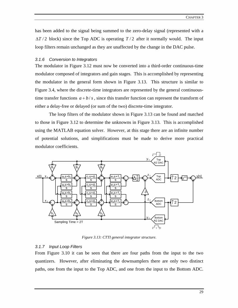
3.1 The Derivation The steps used to derive a low-pass DTTI ∆Σ modulator will be outlined, as well as the
conversion from this modulator to the new CTTI equivalent ∆Σ modulator. While a
specific modulator will be used throughout the derivation, the principles of each step will
be general enough to design other modulators with this technique.
3.1.1 Design The derivation of the DTTI modulator begins with designing a modulator to meet the
desired specifications. The ∆Σ toolbox in MATLAB [16] is used to design a ∆Σ
modulator with the required SQNR by adjusting parameters such as the OSR, the order,
the number of levels in the quantizer, and the out of band gain. To obtain a resolution of
10-bits, an SQNR of more than dB62 is required. Using an OSR of 10, a 16-level (4-bit)
CHAPTER 3
20
quantizer, and a third-order low-pass modulator, a peak SQNR of about dB71 is achieved
(i.e., the SNR achievable with quantization noise limiting the resolution), with a dynamic
range of dB73 (see Appendix A for a description of dynamic range). A plot of the
SQNR versus the input amplitude is shown in Figure 3.1.
-80 -70 -60 -50 -40 -30 -20 -10 0-10
0
10
20
30
40
50
60
70
80
Input Amplitude (dBFS)
SQ
NR
(dB
)
Figure 3.1: Maximum achievable SQNR plot.
The resulting NTF generated to meet these specifications is 31 )1()( −−= zzH .
This NTF has a peak out of band gain of 8 (at 2/sf when 1−=z ). From [17] the
maximum stable input range ][nx of a multibit modulator should be at least:
NhNnx /)1(][max1
−+≤ (3.1)
where ∑∞
=
=0
1][
nnhh , N is the number of levels in the quantizer, and a normalized
feedback between 1± is used. For the given NTF, 81=h and 16=N , resulting in a
maximum stable input signal amplitude of at least 0.5625. However, the input is stable
up to 0.625, or dB08.4 below full-scale ( )08.4 dBFS− . Simulations in MATLAB result
in a peak SQNR of dB5.70 , similar to the peak SQNR found with the ∆Σ toolbox.
ADC
DAC
x[n] y[n]
Sampling Time = T
z3 z2 + z -3 3-z2 + z -3 3 1-
z3 z2 + z -3 3-1
1
1
Figure 3.2: Discrete-time modulator.
CHAPTER 3
21
With an STF of 3)( −= zzG (a 3-sample delay of the input signal), the ∆Σ
modulator is shown in Figure 3.2 with the desired loop filters, where the sampling time
T refers to the sampling period of the ADC, the DAC and the filters ( fTjez π2= ). With
these loop filters, a cascade-of-integrators feedback (CIFB) [16] ∆Σ modulator can be
designed, shown in Figure 3.3. The time-interleaved (by two) equivalent of this
modulator is derived using the techniques described in Section 2.3.2, and is shown in
Figure 3.4. Only six integrators need to be used as opposed to the twelve illustrated, but
this is a more explicit structure to understand all of the integrations involved. The
multiplexing on the output with the upsamplers and delay simply involves a rotary switch
that switches between the top and bottom outputs at the effective sampling frequency.
3 3
ADC
DAC
x[n] y[n]1z - 1
1z - 1
1z - 1
Sampling Time = T
Figure 3.3: Discrete-time CIFB modulator.
3 3
ADC
DAC
3 3
ADC
DAC
1 1 1z - 1
111
z
1
z
1
z
1z - 1
z - 1
z - 1
z - 1
z - 1
z - 1
z - 1
z - 1
z - 1
z - 1
z - 12
2
z-1/2
x[n]
Sampling Time = 2T
x 1
x 2
y 1
y 2
z 2
z 1
2
2 y[n]z-1/2
Figure 3.4: DTTI modulator.
When deriving the NTF, it can be derived with optimization, meaning that the
NTF zeros can be placed optimally in the signal band to maximize the SQNR of the
modulator. The difference would be that in Figure 3.3, an extra path from the output of
the third integrator to the input of second integrator would exist. For this particular
CHAPTER 3
22
modulator, the SQNR would be increased by dB5 . However, this greatly complicates the
time-interleaved loop filters (discussed in the following sections), and in the general case
solutions may not exist in the conversion to continuous-time loop filters (no solution was
found for the optimized version of the ∆Σ modulator used here).
3.1.2 Discrete-Time Loop Filters The first step in obtaining the continuous-time equivalent of the discrete-time modulator
is to determine the loop filters of the DTTI ∆Σ modulator. In this case, the modulator is
time-interleaved by two, meaning that eight loop filters are required (the order of the
modulators has no effect on the number of loop filters, but it adds to the complexity of
deriving them). Referring to Figure 3.4, the loop filters are from 1x to 1z , 1x to 2z , 2x to
1z , 2x to 2z , 1y to 1z , 1y to 2z , 2y to 1z , and 2y to 2z . These loop filters can be
solved manually, or with the help of a program such as MATLAB. A relatively simple
MATLAB script was used to determine the loop filters, and the resulting ∆Σ modulator is
shown in Figure 3.5. It should be noted that since the loop filter from 2y to 1z has a
zero-delay path with a gain of 3− , it has been divided into a sum of two paths, one with
the zero-delay gain of 3− , and the other with the remaining portion of the loop filter.
ADC
DAC
ADC
DAC
2
2
z-1/2
x[n]
Sampling Time = 2T
x 1
x 2
y 1
y 2
z 2
z 1z +13z3 z2+ z -3 3 1-
z2+ z3z3 z2+ z -3 3 1-
z +3z3 z2+ z -3 3 1-
z3 z2+ z -3 3 1-
z3 z2+ z -3 3 1-
z2- z-3z3 z2+ z -3 3 1-
z3 z2+ z -3 3 1-
z +13
z2+ z -6 3 1-
z2+ z -6 3 1-
z3 z2+ z -3 3 1--3+ z2+ z -10 9 3-
2
2 y[n]z-1/2
Figure 3.5: DTTI modulator loop filters.
3.1.3 Elimination of Downsamplers The discrete-time loop filters need to be converted to continuous-time loop filters, but
there still remain downsamplers as well as a delay on the input. This is clearly not
suitable for continuous-time signals, so these blocks must be removed from the discrete-
CHAPTER 3
23
time modulator. It will be shown that this does not appreciably affect the SQNR of the
output, but it does have some consequences. The modulator to be analyzed without these
discrete-time blocks is shown in Figure 3.6.
ADC
DAC
ADC
DAC
x[n]
Sampling Time = 2T
x 1
x 2
y 1
y 2
z 2
z 1z +13z3 z2+ z -3 3 1-
z2+ z3z3 z2+ z -3 3 1-
z +3z3 z2+ z -3 3 1-
z3 z2+ z -3 3 1-
z3 z2+ z -3 3 1-
z2- z-3z3 z2+ z -3 3 1-
z3 z2+ z -3 3 1-
z +13
z2+ z -6 3 1-
z2+ z -6 3 1-
z3 z2+ z -3 3 1--3+ z2 + z -10 9 3-
2
2 y[n]z-1/2
Figure 3.6: DTTI modulator without input downsamplers or delay.
The removal of the downsamplers alters the STF while leaving the NTF
unchanged (since the NTF is unrelated to the input loop filters). Without the
downsamplers or the delay block, each input loop filter processes a sample every T2 , the
sampling period of the input loop filters. However, as opposed to operating on
alternating samples (in Figure 3.5 each input loop filter processes a sample every T2 , but
1x includes samples at T , T3 , T5 , etc. while 2x includes samples at T2 , T4 , T6 , etc.),
every input loop filter processes the same samples. To differentiate between these two
cases, the STF of both will be shown.
With the downsamplers and delay still present on the input, the STF of the
modulator in Figure 3.5 is the same as that in Figure 3.2 due to the equivalence of the
time-interleaved structure [1], and was shown in Section 3.1.1 to be 3)( −= zzG .
However, for the modulator in Figure 3.6, the time-interleaved equivalence cannot be
used without the downsamplers on the input. To find the STF, the modulator must be
linearized (i.e., eliminating the ADCs and DACs and replacing them by unity-gain
blocks) and analyzed. The result of the straightforward linearization and reduction of
Figure 3.6 is shown in Figure 3.7.
CHAPTER 3
24
x[n]
Sampling Time = 2T
x 1
x 2
y 1
y 22
2 y[n]z-1/2
z-1
z-2 y'1
y'2
Figure 3.7: Linearized model for the STF.
Even though the input signal ][nx is a discrete-time signal with samples every T
(as in the typical DTTI case of Figure 3.5), the input delays 1−z and 2−z are evaluating
samples every T2 , and this time they are both taking the samples at T2 , T4 , T6 , etc. (or
T , T3 , T5 , etc.). Therefore, half of the samples are missed. So when both of the
signals are upsampled, they will be the same, only one will be a T2 delayed version of
the other. Finally, when the two signals are combined (the top signal being delayed by
T ), the resulting ][ny outputs the input signal repeated once, this repeated signal being
in place of the samples that were missed. An example of the two output signals from the
upsamplers is shown in Figure 3.8, along with the resulting output waveform ][ny .
2T 4T 6T0 10T8T 12T 14T 16T
y'1
y'2 2T 4T 6T0 10T8T 12T 14T 16T
y[n]
Figure 3.8: Time domain of downsampler outputs and the resulting output signal.
This repeated input signal results in a somewhat different STF than in the typical
DTTI case. To find the STF of the new modulator, the time domain relationship between
][ny and ][nx will be found, and then the Fourier transform of this relationship will be
used to find the frequency domain relationship between )(zY and )(zX .
The relationship between ][ny and ][nx is:
⎩⎨⎧
−=
oddeven
nnxnnx
ny]1[
][][ (3.2)
Expressing Equation 3.2 as a single mathematical equation, the following results:
CHAPTER 3
25
( )( ) ( )( )]1[1]1[21][1][
21][ 1 −−+−+−+= − nxnxnxnxny nn (3.3)
Taking the Fourier transform of Equation 3.3, where )(][ ωjFT eXnx ⎯→⎯ ,
)(][ ωjFT eYny ⎯→⎯ , and a few Fourier transform pairs from [12] have been used, the
resulting equation is:
( ) ( ))()(21)()(
21)( )()()( πωπωωωπωωω −−−−− −++= jjjjjjj eXeeXeeXeXeY (3.4)
Simplifying Equation 3.4 results in the following expression for the magnitude of )( ωjeY
as a function of )( ωjeX :
|))(||)()(|2cos(|)(| )( πωωω ω −+= jjj eXeXeY (3.5)
Equation 3.5 indicates that the output spectrum )( ωjeY includes )( ωjeX as well as a
replica of )( ωjeX at πω = (with a normalized frequency scale). Both the signal
)( ωjeX and its replica are reduced slightly by the modulating signal )2cos(ω , which
keeps the signal power equal to that of the regular time-interleaved case (where the
downsamplers were still present). A sample spectrum is shown in Figure 3.9.
πωoωo 0
Input Signal
Input SignalReplica
-
|cos(ω/2)|
ωoπ- ωoπ+πωoπ- ωoπ+- -- 2π
Figure 3.9: Effects on STF of eliminating downsamplers on input.
In a more general case, for a modulator time-interleaved by a factor M , when all
the inputs are tied together (i.e., eliminating the downsamplers and delays on the input),
the resulting output spectrum will include M replicas of the input signal evenly
distributed in the frequency range from 0 to π2 (normalized). These replicas will have a
modulating signal equal to the magnitude of the sequence
Me
Me
Me
Me
M
MjjjM
n
jnωωω
ω)1(21
0
11 −−
=
++++=∑ K . It can be seen that for the case where
2=M , this sequence reduces to )2cos(|2/2/1| ωω =+ je . For a discrete-time
implementation of a ∆Σ modulator using this STF, the replicas do increase the
CHAPTER 3
26
requirements on the anti-aliasing filter since the input signal bandwidth cannot overlap
with the replicas (see Figure 3.9).
At first it may seem that this STF will reduce the desired in-band signal, but for an
OSR of 10, the maximum attenuation (for 2=M ) is )20/cos(π , which is less than
dB11.0 (the replica is attenuated by at least )20/9cos( π , or dB16 ). This is comparable
to the amplification or attenuation that results in a typical continuous-time ∆Σ modulator
where the STF is not perfectly flat in the signal band.
In another method of eliminating the input downsamplers on the input of a DTTI
modulator, [8] presents the zero-insertion interpolation method. With this method, for a
time-interleaving factor of M , the first input has a gain of M while the other )1( −M
inputs have a zero input. This results in a modulator where, similarly, M replicas occur
between 0 and π2 . However, the difference is that no modulating signal exists, meaning
that no attenuation on the input signal or the replicas occurs. This is less desirable since
it was shown that the attenuation on the input signal due to the modulating signal was
negligible, while the replicas were attenuated by more than dB16 (for )10=OSR .
Therefore, using the zero-insertion interpolation method from [8], the requirements on the
anti-aliasing filter would be greater still. While this technique is a method of eliminating
the downsamplers for continuous-time operation, it was not used for the reasons stated.
3.1.4 Continuous-Time Loop Filters The next step is to convert the discrete-time loop filters to continuous-time loop filters.
The conversion is performed using the technique outlined in Section 2.2.1 with the z-
transform. The equivalent modulator is shown in Figure 3.10 where the continuous-time
loop filters have replaced the discrete-time loop filters of Figure 3.6. The zero-delay path
maintains its gain of 3− while the remainder of this loop filter from 2y to 1z has been
converted appropriately to its continuous-time equivalent. Note that for clarity, the loop
filters have been shown with s , 2s and 3s terms as opposed to Ts , 22sT and 33sT
terms, effectively assuming that 1=T . The remaining figures containing continuous-
time filters have been illustrated in the same way where the transformation Tss →
should be used to properly represent these filters.
CHAPTER 3
27
BottomADC
BottomDAC
TopADC
TopDAC
x(t)
Sampling Time = 2T
x 1
x 2
y 1
y 2
z 2
z 1
s312s2- s -17 15 6-
-3+ s2- s-35 21 6-
s312
s312
s312
s312
s312
s312
s312
s2- s -17 15 6-
s2- s -5 9 6-
s2- s+3 6-
s2- s+5 9 6
s2+ s+3 6-
s2- s+3 6- 2
2 y[n]z-1/2
Figure 3.10: CTTI modulator loop filters.
3.1.5 Return-to-Zero DAC In the discrete-time modulator shown in Figure 3.4, there exists a path from the bottom
quantizer to the top quantizer with no delay. Practically, this cannot be realized since it
involves the instantaneous quantization of the signal in the bottom quantizer, and the
instantaneous transmission of this quantized signal to the top quantizer to be quantized at
the same instant. However, in the discrete-time approach realized by [1], the two phases
of the sampling clock allows both quantizers to be sampled on alternate clock phases,
eliminating this problem.
In continuous-time ∆Σ modulators, the entire pulse fed back by the DAC is
integrated, and thus the finite delay between the quantizer and the DAC output causes
excess loop delay [13]. One way to alleviate this problem is to use an RZ DAC. But due
to the zero-delay path from the output of the Bottom ADC to the input of the Top ADC
that still exists in the continuous-time modulator shown in Figure 3.10, a modification to
the RZ DAC pulses of the ∆Σ modulator must be made. The solution used to overcome
this problem is to clock the quantizers at different times using two different RZ DACs.
This allows the Bottom ADC to quantize its input, and then send it to the summer at the
input of the Top ADC, which then quantizes its value slightly after the quantization in the
Bottom ADC. Following this, the Top DAC then outputs its signal with a RZ pulse after
the appropriate quantization has been performed. As long as enough time between the
two clocks of the two quantizers is given for the Bottom ADC to quantize, the Bottom
CHAPTER 3
28
DAC to convert the signal, and for the summer to sum the Bottom DAC signal and the
modulator signal, then the zero-delay path problem can be eliminated.
BottomRZ DAC
0 T 2T 3T 4T 5T 6T 7T 8T 9T
TopRZ DAC
Q
Q
Q
Q
Q
Q
Q
Q
Q
Q
Figure 3.11: RZ DAC clocking scheme.
The timing for this solution was chosen as follows, assuming T is the sampling
time of the discrete-time modulator shown in Figure 3.3: the clocks of the quantizers
(operating with a period of T2 since this modulator is time-interleaved by 2) are offset
by 2/T , while their respective DACs feedback the signals for a duration of T , waiting
2/T after their respective quantization is performed (to eliminate the excess loop delay).
The output of the DACs is zero for the other T of the full T2 period. This timing is
illustrated in Figure 3.11. The Q’s represent when the quantization is performed in the
respective branches.
BottomADC
BottomRZ DAC
TopADC
TopRZ DAC
x(t)
Sampling Time = 2T
x 1
x 2
y 1
y 2
z 2
z 1
s312s2- s-71 60 24-
s312
s312
s312
s324
s324
s324s2- s -104 72 24-
s2- s-44 48 24-
s2- s+3 6-
s2- s+5 9 6
s2+ s+3 6-
s2- s+3 6-
0 T 2T
0 T 2T
s324s2- s -143 84 24-
-3
2
2 y[n]z-1/2T
2
Figure 3.12: New loop filters with RZ DACs.
The resulting modulator loop filters must be modified to accommodate the change
in the shape of the feedback pulses. This is performed using the techniques outlined in
Section 2.2.2 where the feedback pulses start at 2/T ( 2/T=α ) and end at 2/3T
( 2/3T=β ) for the Bottom DAC, and start at T ( T=α ) and end at T2 ( T2=β ) for
the Top DAC. The resulting modulator is shown in Figure 3.12. An extra delay of 2/T
CHAPTER 3
29
has been added to the signal being summed to the zero-delay signal (represented with a
2/T∆ block) since the Top ADC is operating 2/T after it normally would. The input
loop filters remain unchanged as they are unaffected by the change in the DAC pulse.
3.1.6 Conversion to Integrators The modulator in Figure 3.12 must now be converted into a third-order continuous-time
modulator composed of integrators and gain stages. This is accomplished by representing
the modulator in the general form shown in Figure 3.13. This structure is similar to
Figure 3.4, where the discrete-time integrators are represented by the general continuous-
time transfer functions sba /+ , since this transfer function can represent the transform of
either a delay-free or delayed (or sum of the two) discrete-time integrator.
The loop filters of the modulator shown in Figure 3.13 can be found and matched
to those in Figure 3.12 to determine the unknowns in Figure 3.13. This is accomplished
using the MATLAB equation solver. However, at this stage there are an infinite number
of potential solutions, and simplifications must be made to derive more practical
modulator coefficients.
h h
g g
sx(t)
Sampling Time = 2T
x 1
x 2
sa1 b1+
ssa2 b2+
ssa3 b3+
ssa4 b4+
ssc1 d1+
ssc2 d2+
ssc3 d3+
ssc4 d4+
sse1 f 1+
sse2 f 2+
sse3 f 3+
sse4 f 4+ Bottom
ADC
BottomRZ DAC
TopADC
TopRZ DAC
y 1
y 2
z 2
z 1
0 T 2T
0 T 2T
-3
g
h
1 2 3
1 2 3
2
2 y[n]z-1/2T
2
Figure 3.13: CTTI general integrator structure.
3.1.7 Input Loop Filters From Figure 3.10 it can be seen that there are four paths from the input to the two
quantizers. However, after eliminating the downsamplers there are only two distinct
paths, one from the input to the Top ADC, and one from the input to the Bottom ADC.
CHAPTER 3
30
Therefore, the pairs of loop filters in these paths are summed, resulting in the modulator
shown in Figure 3.14.
BottomADC
BottomRZ DAC
TopADC
TopRZ DAC
x(t)
Sampling Time = 2T
x 1
x 2
y 1
y 2
z 2
z 1
s312s2- s-71 60 24-
s312
s324
s324
s324s2- s -104 72 24-
s2- s-44 48 24-
s2 +2 12-
s2- s+12 124
0 T 2T
0 T 2T
s324s2- s -143 84 24-
-3
2
2 y[n]z-1/2T
2
Figure 3.14: Reduction of input loop filters.
s
a1
b1
sb3
a2
a3
a4
ssa1 b1+
ssa2 b2+
ssa3 b3+
ssa4 b4+ (if b =k b and b =k b )12 34
k1
k2
1 2
Figure 3.15: Integrator simplification.
3.1.8 Integrator Mismatch In Figure 3.13, there are twelve continuous-time integrators. But there are only six
integrations that need to be performed. These twelve integrators are only present due to
the explicit method used to derive the CTTI modulator. However, in the arrangement
shown in Figure 3.13, it is worth noting that each pair of integrators that enter the
summer must have no mismatch. This is not a problem since one integrator with two
feedthrough paths may represent each pair of integrators that get summed together. This
eliminates the mismatch between the two integrators, and halves the number of required
CHAPTER 3
31
integrators to six. Referring to Figure 3.15, the two integrators sba /11 + and sba /22 +
may be represented by one integrator since 2b can be expressed as 112 bkb = . The
equivalent structure shown in Figure 3.15 can be implemented easily with active-RC
integrators. Simplifying the modulator in Figure 3.13 to this structure (for 121 == kk ),
the modulator is now as shown in Figure 3.16.
h h
g g
x(t)
Sampling Time = 2T
x 1
x 2 BottomADC
BottomRZ DAC
TopADC
TopRZ DAC
y 1
y 2
z 2
z 1
0 T 2T
0 T 2T
-3
g
h
1 2 3
1 2 3
s
a1
b1
sb3
a2
a3
a4
s
c1
d1
sd3
c2
c3
c4
s
e1
f 1
sf 3
e2
e3
e4
2
2 y[n]z-1/2T
2
Figure 3.16: Continuous-time modulator with integrator simplification.
3.1.9 DC offsets One difficulty in realizing the modulator shown in Figure 3.16 is that the DC offsets in
the integrators can lead to instability in the modulator. This problem is encountered in
[1] where coefficients (that are less than one) are used on the cross-coupling paths to
reduce the gains between the upper and lower paths in the DTTI modulator. This allows
both the upper and lower paths in the modulator to eliminate their respective DC offsets
(as in a typical ∆Σ modulator). Since the effect of the DC offset of the opposing path is
reduced when each of the cross-coupling coefficients are slightly less than the desired
value, the DC offset influences the path in which it is present more than it influences the
opposite path. This allows the feedback to negate the offset in each path in the same way
that a typical ∆Σ modulator compensates for DC offsets. The problem with this solution
is that it reduces the SNR of the modulator by several decibels, depending on the order of
the modulator and the coefficients used [1].
CHAPTER 3
32
(if k =k =k)1 2
a1
a4
a2
a3
s
a1
b1
sb3
a2
a3
a4
k1
k2 k
sb1
b3b1
Figure 3.17: Integrator simplification to eliminate DC offset instability.
h h
g g
x(t)
Sampling Time = 2T
x 1
x 2 BottomADC
BottomRZ DAC
TopADC
TopRZ DAC
y 1
y 2
z 2
z 1
0 T 2T
0 T 2T
-3
g
h
1 2 3
1 2 3
a1
a4
sb1
a2
a3
c1
c4
sd1
c2
c3
e1
e4
sf 1
e2
e3 2
2 y[n]z-1/2T
2
Figure 3.18: CTTI modulator with only three integrators.
To overcome this weakness of the DTTI modulator in the continuous-time
approach, the upper and lower integrators can be combined so that the DC offset exists in
only one path. Therefore, with a DC offset present, there is no other path to influence it,
and the modulator acts as a typical ∆Σ modulator would, where the negative feedback
works to eliminate the DC offset. This can be accomplished by using the simplification
illustrated in Figure 3.17. If the gains 1k and 2k are equal, then the two paths can be
combined into one. This equivalent integrator as shown can not be implemented with a
single active-RC integrator since there are still some remaining feedthrough gain
coefficients, but once all the simplifications have been made, they can be accumulated as
CHAPTER 3
33
gains from the input feeding into different stages of the modulator. Figure 3.18 illustrates
the implementation of the simplification in Figure 3.17 (for 1=k and 31 bb = ) to reduce
the number of integrators to three.
3.1.10 Evaluating the Unknowns To reduce Figure 3.18 to a structure that employs active-RC integrators (or even Gm-C
integrators), the unknown coefficients can be evaluated to reduce the complexity of the
modulator, facilitating the manipulation of the modulator.
The weakness of the modulator shown in Figure 3.18 is the number of additional
coefficients and summation blocks. The summation blocks that exist after the third
integrator increase the complexity of the modulator since two extra summers are needed.
Furthermore, any coefficient that is not zero will slightly increase the complexity of the
modulator. With these two concerns in mind, and since an infinite number of solutions
exist for the coefficients, a possible solution that maximizes the number of zeroed
coefficients while also eliminating one of the summers after the third integrator (by
setting 3e and 4e to zero) is shown in Figure 3.19. Eliminating the zero gain blocks as
well as the summer reduces the modulator to that shown in Figure 3.20.
-33/4 0
85/4 0
x(t)
Sampling Time = 2T
x 1
x 2 BottomADC
BottomRZ DAC
TopADC
TopRZ DAC
y 1
y 2
z 2
z 1
0 T 2T
0 T 2T
-3
2
2
-151/24
7/6
2s1
143/24
-11/6
0
0
2s1
-1
0
0
0
2s1
1
0 2
2 y[n]z-1/2T
2
Figure 3.19: A potential solution for the unknowns.
The modulator can then be rearranged to eliminate all of the feedthrough gains
that bypass the integrators. These can all be collected as gains being fed in straight from
the input to later stages in the modulator. Also, any path from a DAC that traverses a
CHAPTER 3
34
gain stage and bypasses an integrator (via a gain stage) can be implemented as a gain
from the DAC into the following integrator stage. After these manipulations have been
completed, the resulting modulator is shown in Figure 3.21 with only three integrators
and one extra summer. There are also two extra paths from the input to the inputs of
second and third integrators.
-33/4
85/4
x(t)
Sampling Time = 2T
x 1
x 2 BottomADC
BottomRZ DAC
TopADC
TopRZ DAC
y 1
y 2
z 2
z 1
0 T 2T
0 T 2T
-3
2
2
-151/24
7/6
2s1
143/24
-11/6
2s1
2s1
2
2 y[n]z-1/2T
2
Figure 3.20: Elimination of zero gain blocks and summer.
6
5 11
Sampling Time = 2T
BottomADC
BottomRZ DAC
TopADC
TopRZ DAC
y 1
y 2
z 2
z 1
0 T 2T
0 T 2T
-3
2
2
2s1 2
2s1
2s12 2x(t)
3
7112
2/32
2 y[n]z-1/2T
2
Figure 3.21: Final modulator after rearranging coefficients.
3.1.11 Dynamic Range Scaling The last practical issue that needs to be addressed is the dynamic range at the output of
the integrators. The output range of the integrators should be approximately the same, at
around mV800 - mV1000 (this number was used assuming the use of active-RC
CHAPTER 3
35
integrators with output stages that allow fairly large output swings, even at supply
voltages of V6.1 ). Each of the coefficients is modified to realize this desired range. A
histogram of the three integrator outputs is shown in Figure 3.22, illustrating the
similarity between all of the output swings.
-0.5 -0.4 -0.3 -0.2 -0.1 0 0.1 0.2 0.3 0.4 0.50
500
1000
Output Swing (V)
a)
-0.5 -0.4 -0.3 -0.2 -0.1 0 0.1 0.2 0.3 0.4 0.50
500
1000
1500
Output Swing (V)
b)
-0.5 -0.4 -0.3 -0.2 -0.1 0 0.1 0.2 0.3 0.4 0.50
500
1000
1500
Output Swing (V)
c)
Figure 3.22: Histogram of integrator outputs. a) Int.1 b) Int.2 c) Int.3
3
11
Sampling Time = 2T
BottomADC
BottomRZ DAC
TopADC
TopRZ DAC
y 1
y 2
z 2
z 1
0 T 2T
0 T 2T
-3s1 1/2 s
1s12x(t)
3
7112
1/12
12
52
2
2
1/2
1/4
1/162
2 y[n]z-1/2T
2
Figure 3.23: Final modulator after scaling the integrator output ranges.
The final modulator is shown in Figure 3.23 (not shown in the figure is the gain of
1/2 in the Bottom ADC, while the Top ADC has a gain of 1). This final modulator may
not look entirely like a time-interleaved ∆Σ modulator since there is only one path of
integrators. But it has been shown that this single-path modulator has made use of
simplifications available due to the presence of continuous-time loop filters. Both DACs
CHAPTER 3
36
and ADCs are operating at a sampling frequency of 2/sf (assuming sfT /1= ), as
opposed to sf , and the effective OSR is equal to os ff 2/ , even though with a sampling
frequency of 2/sf the OSR should only be os ff 4/ . An extension to a single-path DTTI
modulator is briefly covered in Appendix B.
3.1.12 Signal and Noise Transfer Functions The STF in the CTTI modulator is not the same as that of the DTTI modulator, as is
always true when a discrete-time ∆Σ modulator is converted to its continuous-time
equivalent. It is more complicated in the CTTI modulator to find the STF because of the
two feedback paths. The NTF is, however, unchanged. This is because the quantizer
sampling turns the feedback loop into a sampled system, which can be represented with
discrete-time transfer functions, and is equivalent to the original DTTI modulator.
Therefore, the four feedback loops in the CTTI modulator (i.e., the four possible paths
from the output of the two quantizers to the input of the two quantizers) will be exactly
the same is in Figure 3.5, and it is these filters that dictate the NTF.
The STF is simply the NTF multiplied by the input loop filter )(zA (see
Equations 2.1 and 2.2). However, for the continuous-time case, a formal manipulation of
the equation results in [18]:
)()( zHsAG C= (3.6)
where )(sAC is the continuous-time input loop filter, and G and H are the STF and
NTF, respectively. For an expression as a function of the frequency f , the substitutions fjez π2= and fjs π2= can be used, resulting in:
)()2()( 2 fjC eHfjAfG ππ= (3.7)
For the CTTI modulator, 31 )1()( −−= zzH . But since the continuous-time input loop
filters )(sAC are broken up into two inputs, this relationship for )(zH cannot be used.
Instead, the system shown in Figure 3.24 must be used, which is a simplified linear model
of Figure 3.6 with the continuous-time input loop filters of Figure 3.14.
After analyzing this figure, the resulting STF is:
CHAPTER 3
37
2)(
)(2
)()(
2)(
)(2
)()(
24
2
23
11
22
2
21
2zH
sAzH
sAzzH
sAzH
sAG CCCC ++⎥⎦
⎤⎢⎣
⎡+= − (3.8)
The 2z terms in 1H , 2H , 3H and 4H represent the upsampling that has occurred.
Making the substitutions fjs π2= and fjez π2= ( fjez π2= for the 1−z delay is the same
as fjez π4= for the 2/1−z in the figure), the resulting STF can be found. A plot for this
STF is shown in Figure 3.25 where the nulls at the normalized frequencies K,3,2,1=f
illustrate the inherent anti-aliasing filter in the CTTI modulator. In this STF, there is a
slight dB81.0 peak at 29.0=f .
x(t)
Sampling Time = 2T
s312
s312s2 +2 12-
s2- s+12 124 2
2 y[n]z-1/2
zz+3H (z)=1
A (s)=C2
A (s)=C1
z-3z-1H (z)=2
zH (z)=3
zz+3H (z)=4
-3z-12
Figure 3.24: System used to find STF.
0 0.5 1 1.5 2 2.5 3 3.5 4-100
-90
-80
-70
-60
-50
-40
-30
-20
-10
0
10
Frequency (normalized to fs)
Gai
n (d
B)
Figure 3.25: CTTI modulator STF.
Simulations were used to find the magnitude of the replica signal, which is still
present in the CTTI modulator. Figure 3.26 illustrates the magnitude of the replica signal
CHAPTER 3
38
for a given input frequency (the STF is also plotted in the background). It should be
remembered, however, that the replica actually appears in the output spectrum at
os ff −2/ for an input frequency of . The point of this graph is to demonstrate that,
despite having the replica in the output spectrum, the inherent anti-aliasing still exists.
Nulls in the replica signal occur at the appropriate frequencies to eliminate out of band
signals that would otherwise alias into the signal band.
0 0.5 1 1.5 2 2.5 3 3.5 4-100
-90
-80
-70
-60
-50
-40
-30
-20
-10
0
10
Gai
n (d
B)
Input Frequency (normalized to fs)
STFReplica
Figure 3.26: Replica magnitude versus input frequency.
3.2 MATLAB Simulations In this section, results from a system level MATLAB simulation of the new CTTI ∆Σ
modulator will be presented, as well as the results when various non-idealities are added.
These non-idealities will include finite-gain operational amplifiers (opamps), the addition
of first and second poles in the opamps, integrator coefficient mismatch, DAC mismatch,
DAC path mismatch, mismatch in the comparators of the flash ADCs, DC offsets in the
integrators, and DAC clock jitter. Furthermore, to properly evaluate the new CTTI
modulator, results are also obtained for an equivalent regular (i.e., non-time-interleaved)
continuous-time (CTreg) ∆Σ modulator that is shown in Figure 3.27. RZ DACs are used
in this modulator to compensate for the excess loop delay, and a 4-bit quantizer is used.
Since the design of the CTTI modulator involves many decisions that may be
changed after simulating blocks at the transistor level, some decisions about the design
(such as the use of active-RC integrators, or the use of capacitive tuning) have been
CHAPTER 3
39
presented without justification, and they will be explained in Chapter 4 where the circuit
level design of the modulator is explained. To avoid any confusion about the modulator
that is to be simulated, the key features of the modulator are that it is a third-order CTTI
∆Σ modulator with two 4-bit quantizers implemented as flash ADCs, seven current mode
DACs for each of the feedback terms (in Figure 3.23), and three active-RC integrators.
Sampling Time = T
ADC
RZDAC
0 T/2 T
s1
s1
s1x(t)
11524
1/3
2
1/4 y[n]
92
Figure 3.27: Regular continuous-time modulator for comparison.
For every simulation that is run, results are obtained for the CTTI modulator
where MHzf s 200= ( MHzf effs 400, = ) and the OSR is 5 (effectively 10), resulting in a
maximum input signal of MHz20 . The regular modulator will be operated at
MHzf s 400= with an OSR of 10, resulting in the same maximum input signal of
MHz20 .
Before proceeding, a note on the MATLAB simulations is in order. Each of the
MATLAB output spectra are obtained with the average of four 5120-point FFTs of the
time-domain output. A Hanning window is used and the signal power for the SNDR is
calculated with the three signal points characteristic of the Hanning window. To compute
the noise and distortion in the SNDR, the noise floor and the distortion terms are added
together (see Appendix A for a description of SNDR). All inputs are dBFS1.4− , equal
to 62.5% of a full scale DAC feedback pulse, unless otherwise noted. The input signals
are at MHz5.2 so that in-band harmonics (if they exists) will deteriorate the SNDR.
3.2.1 Ideal System The ideal systems of Figure 3.23 and Figure 3.27 were simulated and the output spectra
of both the CTTI and the regular ∆Σ modulators are shown in Figure 3.28. In these
simulations, an SNDR of dB7.70 is obtained for both modulators. These spectra will be
used as a reference for the next several sections.
CHAPTER 3
40
100 101 102-200
-180
-160
-140
-120
-100
-80
-60
-40
-20
0
Frequency (MHz) (fs,eff=400MHz)
Am
plitu
de (d
B)
a)
100 101 102-200
-180
-160
-140
-120
-100
-80
-60
-40
-20
0
Frequency (MHz) (fs=400MHz)
Am
plitu
de (d
B)
b)
Figure 3.28: Ideal output spectra. a) CTTI b) CTreg
3.2.2 Finite-Gain Opamps An active-RC integrator with an ideal opamp will have a transfer function:
sCRsTF 1)( −= (3.9)
However, when the effects of finite opamp gain are considered, the transfer function
becomes [19]:
AsCR
AA
sTF1)1(
1)(+
+−
= (3.10)
where A is the finite opamp gain. The finite opamp gain increases the noise floor. With
an opamp gain of dB45 ( 178=A ), the output spectra of both modulators are shown in
Figure 3.29. The increase in the noise floor is evident for the CTTI modulator. The
SNDR has degraded by about dB3 to dB7.67 .
100 101 102-120
-100
-80
-60
-40
-20
0
Frequency (MHz) (fs,eff=400MHz)
Am
plitu
de (d
B)
a)
100 101 102-200
-180
-160
-140
-120
-100
-80
-60
-40
-20
0
Frequency (MHz) (fs=400MHz)
Am
plitu
de (d
B)
b)
Figure 3.29: Output spectra for finite-gain opamps. a) CTTI b) CTreg
CHAPTER 3
41
Much less degradation is seen in the regular ∆Σ modulator, where an SNDR of
dB6.69 is obtained. Typically ∆Σ modulators need opamp gains on the order of the OSR
[20], but the CTTI ∆Σ modulator needs a much larger opamp DC gain due to the required
matching between the two feedback paths.
3.2.3 Addition of Opamp Poles To use a more accurate representation of an opamp, a first-pole and second-pole can be
added to the transfer function (the first pole is far more significant in determining the
behaviour of the modulator). This facilitates the design of the opamp at the transistor
level since definite specifications can be found about the desired frequency characteristics
of the opamp.
The poles are introduced by assuming the gain A in Equation 3.10 is frequency
dependent. With a DC gain of oA and a first and second pole frequency of 1Pf and 2Pf ,
respectively, the resulting gain of the opamp is described by:
)/1)(/1( 21 PP
o
ssA
Aωω ++
= (3.11)
where 11 2 PP fπω = and 22 2 PP fπω = . Assuming that RCT = , this results in an integrator
transfer function of:
1)()1(21
2
21
213
21
+++++++
+=
sTTAsTTsTA
TFPPo
PP
PP
PP
o
ωωωω
ωωωω
(3.12)
With a DC gain of dB50 , a first-pole frequency of MHz5 and a second-pole
frequency of GHz1 , the resulting output spectra are shown in Figure 3.30. The SNDR of
the CTTI modulator is dB8.64 . The out of band peaking is one of the effects of the finite
bandwidth opamps since they add a delay to the path from the DACs to the ADCs, as
well as from the input to the ADCs, effectively changing the NTF. This can be partly
compensated by properly advancing the time when the DAC pulses begin, which will be
discussed in Chapter 4.
The regular modulator exhibits a much sharper out of band peak. The output
spectrum in Figure 3.30b has an SNDR of dB3.66 , despite the input being dBFS1.7− (as
opposed to dBFS1.4− ). The input needed to be reduced because with a full-scale input,
CHAPTER 3
42
the modulator was unstable. Therefore, the regular modulator can achieve a higher
SNDR with the addition of first and second poles, but it becomes much more unstable.
Also, with these opamp specifications, the highest frequency operation of the regular
modulator is about MHzf s 500= before it goes unstable for inputs well below
dBFS10− , while the CTTI modulator maintains stability for sampling frequencies above
MHz500 ( GHzf effs 1, = ), even though the SNDR begins to degrade. Furthermore, the
regular modulator can be driven to instability if inputs larger than dBFS22− are input at
the out of band peak frequency where the peaking occurs (about MHz110 for
MHzf s 400= ).
100 101 102-120
-100
-80
-60
-40
-20
0
Frequency (MHz) (fs,eff=400MHz)
Am
plitu
de (d
B)
a)
100 101 102-200
-180
-160
-140
-120
-100
-80
-60
-40
-20
0
Frequency (MHz) (fs=400MHz)
Am
plitu
de (d
B)
b)
Figure 3.30: Output spectra for finite-gain two-pole opamps. a) CTTI b) CTreg
3.2.4 Integrator Coefficient Mismatch To properly design the extent of the capacitive tuning required, the CTTI modulator’s
resilience to incorrect integrator gains is needed. To simulate this, the gain of each
integrator was adjusted by a certain percentage to determine what deviation from the
ideal integrator coefficient was acceptable. The output spectra with the integrators
deviating from the expected values by 2% are shown in Figure 3.31 (the worst case was
found when all capacitors were increased by 2%). For the CTTI modulator, it is evident
that the NTF is altered somewhat, resulting in a slight decrease in the SNDR to dB2.69 .
The regular modulator is barely affected by this change in integrator coefficients, and the
resulting SNDR is dB6.70 . Since the SNDR in the CTTI modulator drops by only
dB5.1 with a 2% deviation in the integrator gains, the minimum sized tuning capacitor
needs to be C04.0 (for a feedback capacitor with capacitance C ).
CHAPTER 3
43
100 101 102-200
-180
-160
-140
-120
-100
-80
-60
-40
-20
0
Frequency (MHz) (fs,eff=400MHz)
Am
plitu
de (d
B)
a)
100 101 102-200
-180
-160
-140
-120
-100
-80
-60
-40
-20
0
Frequency (MHz) (fs=400MHz)
Am
plitu
de (d
B)
b)
Figure 3.31: Output spectra with integrator coefficient mismatch. a) CTTI b) CTreg
3.2.5 DAC Mismatch Before designing the DACs, the required linearity must be determined to properly size
the DAC current cells. Each of the current cells of the seven DACs (before passing
through the appropriate gain stage) was assigned a Gaussian random variable with a mean
of one and a standard deviation equal to a value representing the normalized current
standard deviation IIσ . To reduce the non-linearities caused by DAC mismatch to an
acceptable level, DAC1, DAC2, DAC3 and DAC4 (i.e., the feedback DAC pulses with
gains 2, 2, 3 and 2/5 , respectively) all require a linearity over 10-bits, DAC5 and DAC6
(i.e., the feedback DAC pulses with gains 12/71 and 3/11 , respectively) require a
linearity over 9-bits, and DAC7 (i.e., the feedback DAC pulse with gain 3− ) requires a
linearity over 8 bits. When treated as a 16-level DAC, the linearity of the sum of the 16
current cells results in a 2-bit ( 416/16 = ) increase in the linearity of the individual
current cells. Therefore, the individual current cells require a linearity of at least 8-bits
(DAC1, DAC2, DAC3, DAC4), 7-bits (DAC5, DAC6) and 6-bits (DAC7).
With linearities 0.35-bits higher than the minimum required, the CTTI modulator
obtains a mean SNDR of dB8.66 with a 99% yield having an SNDR greater than
dB4.63 . A sample output spectrum is shown in Figure 3.32a for the CTTI modulator. In
this figure the SNDR is dB6.67 . Both the increase in the noise floor and the harmonics
throughout the spectrum are the effects of DAC mismatch.
Figure 3.32b illustrates a sample output spectrum for the regular modulator. A
very similar SNDR of dB7.67 was obtained in this simulation. However, while the mean
CHAPTER 3
44
SNDR of the regular modulator simulations was almost the same at dB6.66 (with a
similar DAC mismatch for the three DACs), the standard deviation was larger resulting in
99% of the simulations achieving an SNDR greater than only dB3.61 .
The regular modulator has a larger standard deviation because the standard
deviation of the DAC mismatch in the CTTI modulator is effectively smaller. Since the
input of each integrator in the CTTI modulator is the sum of two random DACs, the
standard deviation of the DAC mismatch is proportionally a fraction smaller than that of
the regular modulator (i.e., if the DAC mismatch in both paths were the same, the
standard deviation would increase in the CTTI modulator).
100 101 102-120
-100
-80
-60
-40
-20
0
Frequency (MHz) (fs,eff=400MHz)
Am
plitu
de (d
B)
a)
100 101 102-120
-100
-80
-60
-40
-20
0
Frequency (MHz) (fs=400MHz)
Am
plitu
de (d
B)
b)
Figure 3.32: Output spectra for DAC mismatch. a) CTTI b) CTreg
3.2.6 DAC Path Mismatch The two feedback paths in the CTTI modulator need to be matched to a certain degree to
keep the noise floor low. With too much mismatch between the two DAC feedback
paths, the noise floor rises above the required dB62 . With a mismatch of 0.5%, the
output spectrum of the CTTI modulator (this is not applicable for the regular modulator)
is shown in Figure 3.33, and the SNDR is dB5.64 . The importance of properly matching
these two paths is clear, and matching of better than 0.5% is desired.
3.2.7 Comparator Mismatch The threshold mismatches in the comparators of the flash ADCs are another non-ideality
that can affect the overall modulator performance. This offset can be modeled as an
additional Gaussian random variable that adjusts the comparator threshold values, with a
standard deviation of VTσ .
CHAPTER 3
45
100 101 102-120
-100
-80
-60
-40
-20
0
Frequency (MHz) (fs,eff=400MHz)
Am
plitu
de (d
B)
Figure 3.33: Output spectrum for 0.5% DAC path mismatch.
MATLAB simulations were used to find an appropriate standard deviation with
input swings on the Top and Bottom ADCs of mV100± and mV200± , respectively.
For the CTTI modulator, with a standard deviation of mV6 , the SNDR is dB8.68 on
average, with 99% of the modulators achieving an SNDR greater than dB0.67 . The
results of the regular modulator are slightly better with an SNDR mean of dB7.69 and
99% of them with an SNDR greater than dB5.68 . The output spectra contain some
minor spurs and sample plots are shown in Figure 3.34 where the SNDR for the CTTI
modulator is dB3.65 and the SNDR for the regular modulator is dB4.67 (in these two
simulations a standard deviation of mV12 was used to accentuate the non-idealities).
100 101 102-200
-180
-160
-140
-120
-100
-80
-60
-40
-20
0
Frequency (MHz) (fs,eff=400MHz)
Am
plitu
de (d
B)
a)
100 101 102-200
-180
-160
-140
-120
-100
-80
-60
-40
-20
0
Frequency (MHz) (fs=400MHz)
Am
plitu
de (d
B)
b)
Figure 3.34: Output spectra with comparator offsets. a) CTTI b) CTreg
3.2.8 Integrator Offsets The design of the new CTTI ∆Σ modulator eliminated the second integrator path to
overcome the potential SNDR degradation of the DC offsets in the integrators.
Simulations to assert this design goal were performed by adding a DC term to the
CHAPTER 3
46
summation node at the input of each of the integrators. With a DC offset voltage of
mV10 on the input of each of the integrators, the output spectrum of both modulators is
shown in Figure 3.35. A DC term (not visible) exists in the output spectrum as expected
since the output will no longer vary with an average of exactly zero. It is evident that
there is minimal SNDR degradation in the CTTI modulator with the addition of DC offset
voltages, similar to the regular continuous-time modulator. The SNDR for the CTTI
modulator in Figure 3.35 is dB6.69 , while it is dB5.70 for the regular modulator.
100 101 102-200
-180
-160
-140
-120
-100
-80
-60
-40
-20
0
Frequency (MHz) (fs,eff=400MHz)
Am
plitu
de (d
B)
a)
100 101 102-200
-180
-160
-140
-120
-100
-80
-60
-40
-20
0
Frequency (MHz) (fs=400MHz)
Am
plitu
de (d
B)
b)
Figure 3.35: Output spectra with integrator DC offsets. a) CTTI b) CTreg
3.2.9 DAC Clock Jitter Clock jitter is a major limitation of continuous-time ∆Σ modulators [21]. While the jitter
can affect both the ADC clock and the DAC clock, errors introduced at the ADC are
shaped by the NTF and do not significantly reduce the SNR while errors introduced at the
DAC directly add to the signal, significantly reducing the SNR [22].
100 101 102-120
-100
-80
-60
-40
-20
0
Frequency (MHz) (fs,eff=400MHz)
Am
plitu
de (d
B)
a)
100 101 102-120
-100
-80
-60
-40
-20
0
Frequency (MHz) (fs=400MHz)
Am
plitu
de (d
B)
b)
Figure 3.36: Output spectra for DAC jitter. a) CTTI b) CTreg
CHAPTER 3
47
To simulate this non-ideality, ps3 (rms) of jitter was added to the DAC feedback
clocks in both modulators. The resulting output spectra are shown in Figure 3.36. In this
case, it is quite clear that the jitter degrades the performance of the regular ∆Σ modulator
much more than in the CTTI ∆Σ modulator. The reason for this smaller degradation in
the CTTI modulator is that the clocks are operating at half the speed, and the jitter affects
this modulator as it would a modulator operating at MHz200 . However, since the
regular modulator is operating at twice the speed, the ps3 of jitter at MHz400 has a
more detrimental effect. The SNDR of the CTTI modulator is dB0.64 while it is dB0.60
for the regular modulator.
3.2.10 All Non-Idealities One final simulation was run to incorporate all of the non-idealities mentioned above, as
well as an added noise component to represent a dBFS2.69− input-referred circuit noise,
resulting in an input SNR of dB1.65 . The results are shown below in Figure 3.37 for
both the CTTI modulator and the regular modulator. The CTTI modulator has an SNDR
of dB9.58 while the regular modulator has an SNDR of dB6.51 . The regular modulator
was unstable for input signals larger than dBFS1.16− and therefore the input signal in
Figure 3.37b is dB12 lower than it should be. This problem is most likely due to the
finite opamp bandwidth, as mentioned in Section 3.2.3. It is clear that it would be
difficult to get either modulator to attain the full 10-bits resolution ( dB62 ), but the CTTI
∆Σ modulator can attain an extra full bit of resolution over the regular ∆Σ modulator.
100 101 102-120
-100
-80
-60
-40
-20
0
Frequency (MHz) (fs,eff=400MHz)
Am
plitu
de (d
B)
a)
100 101 102-120
-100
-80
-60
-40
-20
0
Frequency (MHz) (fs=400MHz)
Am
plitu
de (d
B)
b)
Figure 3.37: Output spectra with all non-idealities. a) CTTI b) CTreg
CHAPTER 3
48
A two-tone test was performed to evaluate the effects of distortion on the CTTI
modulator at higher input frequencies. Typically with an input signal frequency greater
than half of the maximum inband signal frequency MAXf , the harmonics are out of band
and do not degrade the SNDR. But if two tones 1f and 2f (where 21 ff < ) are input
appropriately close to MAXf , then the third-order distortion terms remain inband as
intermodulation products with frequencies ff ∆−1 and ff ∆+2 (where 12 fff −=∆ )
[11], and a second-order distortion term remains inband as an intermodulation product at
f∆ . The third-order intermodulation products are ideally dB5.9 above the third-order
distortion term of a single-tone test, while the second-order intermodulation product is
ideally dB6 above the second-order distortion term of a single-tone test (assuming all
input tones are of equal amplitude).
The output spectra are shown in Figure 3.38 where input signals at MHz19 and
MHz5.19 were used. With second and third-order distortion, intermodulation products
should be seen at MHz5.0 , MHz5.18 and MHz20 . The inputs have been reduced by
dB6 (to dBFS1.10− and dBFS1.22− ) to avoid saturating the modulators. The noise
floors show no considerable change from those of Figure 3.37, and the intermodulation
products are barely visible at MHz5.18 and MHz20 . An intermodulation product at
MHz5.0 due to the second harmonic is visible in the CTTI modulator. This
intermodulation product is within a couple decibels of its expected value, given the
amplitude of the second harmonic in Figure 3.37.
0 5 10 15 20 25 30-120
-100
-80
-60
-40
-20
0
Frequency (MHz) (fs,eff=400MHz)
Am
plitu
de (d
B)
a)
0 5 10 15 20 25 30-120
-100
-80
-60
-40
-20
0
Frequency (MHz) (fs=400MHz)
Am
plitu
de (d
B)
b)
Figure 3.38: Output spectra for two-tone input. a) CTTI b) CTreg
CHAPTER 3
49
A simulation was also run with both modulators running at a reduced sampling
frequency of MHz100 ( MHzf effs 200, = ) for the CTTI modulator and MHz200 for the
regular modulator. In this case, the regular modulator was stable for a dBFS1.4− input,
and both modulators obtained very similar results. The CTTI modulator achieved an
SNDR of dB7.58 while the regular modulator had an SNDR of dB4.58 . The output
spectra are shown in Figure 3.39. Since the CTTI modulator’s SNDR is no better than it
was with MHzf effs 400, = , it would appear that the limiting factors are not related to its
speed of operation (these frequency dependent non-idealities would include finite opamp
bandwidth and DAC clock jitter). Also, it is clear that the regular modulator is limited at
this point by its speed of operation, and it is not suited to perform at higher sampling
frequencies, unlike the CTTI modulator.
100 101 102-120
-100
-80
-60
-40
-20
0
Frequency (MHz) (fs,eff=200MHz)
Am
plitu
de (d
B)
a)
100 101 102-120
-100
-80
-60
-40
-20
0
Frequency (MHz) (fs=200MHz)
Am
plitu
de (d
B)
b)
Figure 3.39: Output spectra with all non-idealities at 200MHz. a) CTTI b) CTreg
Table 3-1 summarizes the effects of different non-idealities on each of the
modulators. The most important conclusion drawn from this is that the CTTI modulator
is more suited for higher speed operation.
3.3 Summary The derivation of a third-order CTTI ∆Σ modulator from a DTTI ∆Σ modulator was
presented. After explaining the basic derivation with many potential solutions, a solution
was found that minimized the number of integrators while also reducing the effects of
integrator DC offsets. Various non-idealities were added to the MATLAB models of the
CTTI and regular modulators to determine their effects. These simulations confirmed
that the CTTI modulator would be more suited to higher-speed applications. They also
CHAPTER 3
50
gave indications as to what specifications need to be met at the transistor level design of
the circuit, discussed in the next chapter.
Non-Ideality CTTI SNDR CTreg SNDR Comment Finite Opamp Gain dB7.67 dB6.69 CTreg more resilient
Finite Opamp Bandwidth dB8.64 dB3.66 CTTI better for high- speed operation
Integrator Coefficient Mismatch dB2.69 dB6.70 Similar results DAC Mismatch dB8.66 dB6.66 CTTI higher yield DAC Path Mismatch dB5.64 N/A Less than 0.5% needed Comparator Mismatch dB8.68 dB7.69 CTreg slightly better
Integrator Offsets dB6.69 dB5.70 CTreg unaffected; CTTI resilient to offsets
DAC Clock Jitter dB0.64 dB0.60 CTTI better for high- speed operation
All Non-Idealities ( )400MHz dB9.58 dB6.51 CTTI better for high- speed operation
All Non-Idealities ( )200MHz dB7.58 dB4.58 Similar results
Table 3-1: Non-ideality comparisons.
51
Chapter 4
Circuit Design
Chapter 4 Circuit Design In this chapter, the transistor level design of the new CTTI ∆Σ modulator will be
discussed. The modulator is designed in mµ18.0 CMOS technology with a supply
voltage of V8.1 . The general modulator structure is shown in Figure 4.1. The modulator
has two sampling frequency settings, MHz100 and MHz200 (effectively MHz200 and
MHz400 , respectively). The OSR of the modulator is 5 (effectively 10), allowing a
maximum input signal bandwidth of MHz10 or MHz20 , depending on the sampling
frequency. It was shown in the previous chapter that with these sampling frequencies, a
9.5-bit modulator should be realizable.
TOPADC
BOTTOMADC
DAC
7
DAC
5
DAC
3
DAC
1
DAC
6
DAC
4
DAC
2
S/H
S/H
SUMMERBout
INTout
RZ ctrl
RZ ctrl
Figure 4.1: General circuit schematic.
The major circuit blocks of the modulator include the integrators, the DACs, the
ADCs, the summer and the clock generator. A few other minor blocks include the
thermometer-to-binary decoder, the biasing circuit, and the sample-and-hold circuit (for
CHAPTER 4
52
the 2/T delay). They will all be discussed in the following sections, with a final section
demonstrating some Spice simulation results of the whole circuit.
4.1 The Integrators The primary consideration when designing the integrators is the bandwidth. Based on
MATLAB simulations, a dB3− (first-pole) frequency of at least MHz5 , a second-pole
frequency of at least GHz1 , and a gain of dB50 is required. Furthermore, a single-ended
swing of approximately mV800 to mV1000 is needed at the output of the integrators
based on the dynamic range scaling used throughout the modulator.
One alternative would have been to use Gm-C integrators, which operate at higher
speeds but suffer from reduced linearity [11], an acceptable drawback since the
modulator is only a 10-bit design. However, the swing requirements could not be met
with these integrators for any of the three stages, so they were not used.
To meet the specifications, an active-RC integrator is used. A tunable capacitor
array is used to vary the RC time constant of the integrators to compensate for process
variations as well as the change in sampling frequencies. Furthermore, due to the
differential design, a common-mode feedback circuit is needed, as well as a startup
circuit to eliminate an initial state that could keep the outputs of the opamp at the positive
supply rails.
4.1.1 Resistor and Capacitor Values The resistor and capacitor values are chosen according to noise and bandwidth
considerations. For the first stage, Spice simulations were performed to find a resistor
size that reduced the noise to dBFS70− (this simulation was performed with the DACs
feeding into the first stage integrator to include all front-end noise contributions).
A Ωk5.12 resistor is used from the input to the first stage integrator. Since the
input resistor is scaled to allow an input range of mV1000 peak-to-peak (single-ended),
the resulting capacitor value is fF800 (when using a sampling frequency of MHz200 ).
The second stage uses a fF400 integrating capacitor, and the final third stage uses a
fF100 integrating capacitor. Based on these capacitive values, the resistors are sized
accordingly as shown in Figure 4.2. In a differential design, a negative resistor simply
means that the differential inputs to the subsequent stage are switched [11].
CHAPTER 4
53
ADC
ADC
DA
C7
DA
C5
DA
C3
DA
C1
DA
C6
DA
C4
DA
C2
800fF 400fF 100fF
-12.5k -12.5k
100k
50k
-12.5k
-300k
RZ ctrl
RZ ctrl
Figure 4.2: Capacitor and resistor values for 200MHz operation.
4.1.2 Capacitive Tuning The integrator feedback capacitors are tunable to allow a sampling frequency between
MHz100 and MHz200 . Taking into account a 20% process variation in the resistor and
capacitor values, this means that each feedback capacitor needs to be tunable between
0.69 and 3.13 of the nominal capacitance C (1st stage fFC 800= , 2nd stage fFC 400= ,
3rd stage fFC 100= ). Shift registers are used to input the desired tuning codes for the
capacitor array. The structure is such that one capacitor equal to C64.0 is always
connected in the feedback path. Six bits are needed to realize the appropriate tuning code
within a worst-case deviation of 2% from the required RC time constant (this was found
using MATLAB simulations in Section 3.2.4). Each bit controls a capacitor value that is
C04.0 , C08.0 , C16.0 , C32.0 , C64.0 and C28.1 . From these capacitors, the two
extremes in the potential tuning codes range from C64.0 to C16.3 . The transistor level
design of the capacitor array for the first stage is shown in Figure 4.3 [23]. The reset
switch is used to short out the capacitors and reset the modulator.
4.1.3 Operational Amplifier The opamp is designed to have a gain of about dB50 with a first-pole frequency
of MHz10 (double the required first pole frequency of Section 3.2.3), a unity-gain
frequency of around GHz2 , and an output swing larger than mV800 (single-ended), with
a feedback capacitor of fF800 (for the first integrator stage). A two-stage differential
CHAPTER 4
54
opamp is used since it attains the bandwidth requirements while also achieving the
required output swing and gain.
ctrl<6> ctrl<5> ctrl<4> ctrl<3> ctrl<2> ctrl<1>
reset
512fF
32fF 64fF 128fF 256fF 512fF 1024fF
WL2 W
L4 WL8 W
L16 WL32W
L
Output Nodeof OpAmp
Input Nodeof OpAmp
Figure 4.3: First integrator capacitor array.
One difficulty with alternative opamp configurations is that they can either not
achieve the output swing, or not achieve the required bandwidth. A second stage is
almost surely needed since a reasonably high gain is required, and with a high gain
single-stage opamp, the required swing cannot be met. But once a second stage is added,
the bandwidth is reduced. A compromise between these two difficulties is to use a high-
bandwidth first stage differential pair with a second stage common-source amplifier to
increase the gain [11].
To increase the bandwidth of the first stage of the opamp, it is designed to use
minimum sized PMOS input transistors. PMOS transistors are used since the common-
mode throughout the integrator stages is mV700 (determined due to the sizing
requirements on the PMOS DACs – the DACs would need to have much larger lengths
for the same effective voltage if they were NMOS). The second stage is an NMOS
common-source amplifier with a very high current and minimum sized channel length
transistors. The high current is used to increase the bandwidth of the second stage, while
the high current as well as the minimum sized channel length transistors are used to
reduce the output resistance of the opamp. Since the bandwidth requirements on the
opamp would not allow the use of a third output stage to drive the resistive loads, a low
opamp output resistance (around Ωk1 , reduced further due to feedback by a factor of
βA+1 , where A is the gain of the opamp and β is the feedback factor [19]) is used in
conjunction with relatively large resistors feeding into the subsequent stages of the
CHAPTER 4
55
modulator. Therefore, the inter-stage resistors of at least Ωk10 do not load the relatively
low output impedance of the opamp.
The transistor level design of the two-stage opamp is shown in Figure 4.4 (the
sizes shown are LW ratios, in microns, for the first integrator stage). All three opamps
for the three integrator stages use the same two-stage opamp, and all of the first stages are
identical. However, the second stage of the opamps use different currents (and therefore
different transistor sizes) since they each drive different capacitive loads. The resistor
CR is used for lead compensation, while CC is used for dominant-pole compensation.
inn inp
cmn
outn
outp
VSS
VDD
M1 M2
RC RC CCCC
200Ω200fF 200Ω 200fF80
0.2480
0.24
600.18
600.18
1600.24
600.18
600.18
2400.18
2400.18
Figure 4.4: Two-stage opamp.
A summary of the first stage and second stage currents for each of the three
integrators is shown in Table 4-1, along with the DC gain, the first-pole frequency, the
unity-gain frequency, and the phase margin. The first-pole frequency and the unity-gain
frequency were simulated with the open loop opamp loaded with the corresponding
feedback capacitance (to ground), while the phase margin was found with the open loop
opamp loaded with the proper feedback network.
Integrator First-stage Current
Second-stage Current DC gain First-Pole
Frequency Unity-Gain Frequency
Phase Margin
First uA955 mA49.6 dB9.48 MHz96.9 MHz88.1 o1.60 Second uA955 mA33.4 dB7.48 MHz5.10 MHz99.1 o1.58 Third uA955 mA24.3 dB6.48 MHz9.10 MHz27.2 o1.67
Table 4-1: Integrator specifications.
CHAPTER 4
56
4.1.4 Common-Mode Feedback Since the opamp is a differential design, a common-mode feedback (CMFB) circuit is
required to maintain the proper common-mode at the output of the opamp. The CMFB
circuit used is shown in Figure 4.5. A resistive divider using large resistors ( Ωk20 ) is
used to sense the common-mode of the opamp output voltages ( outp and outn in the
figure), and this common-mode voltage is then compared to the desired common-mode
voltage ( ref node in the figure) through a PMOS differential pair. This circuit is similar
to the one presented in [11].
ref
VSS
VDD
cmn
outp
outn
320.24
20kΩ50fF
20kΩ50fF
120.24
160.24
160.24
120.24
Figure 4.5: Common-mode feedback circuit.
The control voltage ( cmn node in the figure) is fed into the gates of the load
transistors on the first stage of the opamp. However, due to the high gain of the CMFB
circuit, only half of the load transistors are controlled by the CMFB circuit, and the other
half of the transistors are controlled by a constant current source.
4.1.5 Startup Circuit Spice simulations indicated that there exists an undesirable initial state that the opamp
and CMFB circuit may take in the reset mode. If the first stage output of the opamp
(which is not a well controlled voltage) begins low enough to keep the common source
transistor of the second stage off, the output of the second stage goes high. Since the
output is tied to the input (through the reset switch), the input will also be high, and the
output of the first stage will stay low. To fix this problem, the circuit in Figure 4.6 is
used [11]. When the output of the second stage is high, the cmn node in the CMFB is
CHAPTER 4
57
low. In this circuit, the low voltage of the cmn node turns off M1, allowing M4 to turn
on M2 and M3, pulling down the second stage output voltage from its high state.
outp
outn
cmn
VSS
VDD
M4
M1M2 M3
118
20.18
20.18
20.18
Figure 4.6: Startup circuit.
4.2 The Digital-to-Analog Converters The 4-bit current-mode DACs are designed to operate at MHz200 with RZ pulses.
Seven DACs are needed, where the first two are identical and the other five are all unique
in their sizes and full-scale currents. The important issues that arise when designing the
DACs are the magnitudes of the full-scale currents, the sizing of the DACs to achieve the
required linearity, the method of obtaining RZ pulses, and the layout of the DACs. The
seventh DAC will be discussed in a final section, while the first sections will discuss the
design of the other six PMOS DACs.
4.2.1 General The standard DAC current cell used for the first six DACs is shown in Figure 4.7 (the
sizes shown are for DAC1 and DAC2). The output current is fed into the input of the
opamp, while NMOS transistors (not shown) provide the constant DC bias current, equal
to half of the full-scale current. The difference between the NMOS DC bias current and
the current generated by the sum of the 15 PMOS current cells (for a 16-level 4-bit
design) is the current that enters the input of the opamp. Charge injection cancellation
using dummy switches is accomplished with transistors M4 and M5. They are half the
size of M2 and M3.
A cascode current source was considered for the DAC cell, but a few difficulties
arose with this solution. First, due to the size of the single transistor current source, there
was already a fairly high output resistance, and so this benefit of a cascode current source
CHAPTER 4
58
was not needed. Furthermore, the cascode current source required a larger voltage drop
across its two transistors. And in a design where the effective voltage is being
maximized (to reduce the size of the DACs) while remaining concerned with how close
the output voltage is to the common-mode level, the extra voltage required for the
cascoded transistors becomes too large. Also, the design is much simpler when only
biasing a single transistor.
inp
VDD
inn
outn
outp
VSS
M1
M3M2
M4 M5
21.620
1.20.18
1.20.18
0.60.18
0.60.18
Figure 4.7: DAC PMOS current cell.
A PMOS current cell is used since the maximum available channel length in the
Spice models is mµ20 . To achieve the same linearity with an NMOS device, the length
would have needed to be doubled, making the devices too large to properly simulate.
4.2.2 Full-Scale Currents The DAC full-scale currents are derived from the resistor and capacitor values already
chosen for the opamps. Since the DACs are 4-bits, each DAC current cell is required to
supply 15/1 of the full-scale current. The full-scale currents are determined as follows,
using the first DAC as an example (operating at MHz200 ).
The desired voltage signal drawn from the first stage DACs (DAC1 and DAC2) is
mV75.932×± , where the factor of 2 comes from the gain block of the ∆Σ modulator
(see Figure 3.23), and the mV75.93± comes from the unity-gain quantizer, leaving the
upper and lower values 32/1 from the mV100± edges. This voltage signal must then
pass through an integrating block with a transfer function of Ts/1 , where nsT 5.2= .
CHAPTER 4
59
Equating this to a current passing through the feedback capacitor FBC of the opamp, the
equality becomes:
FBsCI
sTmVx ±
=± 75.932 (4.1)
Solving this for the first stage where fFCFB 800= , the result is uAI 60= . Therefore,
the full-scale current is uAI FS 120= , where the desired current signal ranging from
uA60− to uA60 can be generated using an NMOS DC bias current of 2/FSI for the
DAC current cells.
Every DAC full-scale current can be derived using this method, and the results are
as follows: uAI FS 1201 = , uAI FS 1202 = , uAI FS 903 = , uAI FS 754 = , uAI FS 38.445 = ,
uAI FS 5.276 = .
4.2.3 Sizing The DACs are sized according to the linearity requirements of each stage. MATLAB
simulations were used to determine the tolerable mismatch in Section 3.2.5. In 99% of
the simulations, an SNDR of more than dB4.63 was observed with the following
normalized standard deviations in the current values ( II /σ ), where I represents the
individual current cell currents: 0025.0/ 11 =IIσ , 0025.0/ 22 =IIσ , 0025.0/ 33 =IIσ ,
0025.0/ 44 =IIσ , 005.0/ 55 =IIσ , 005.0/ 66 =IIσ .
The relationship between the size of the current cell transistor M1 and the
standard deviation in the currents is (from [24]): 22
2⎟⎠⎞
⎜⎝⎛
⎟⎟⎠
⎞⎜⎜⎝
⎛+
−×
=×I
AVV
ALW I
tGS
VT σβ (4.2)
where TGS VV − is the effective voltage of the transistor, VTA and βA are process
mismatch constants, and W and L are the desired width and length of the transistor. The
effective voltage can vary by about mV200 across process and temperature, so enough
headroom must be left for the common-mode voltage of mV700 ( mV900 below a low
supply voltage of V6.1 ), as well as the voltage drop across the switching transistors of
the DAC current cell. However, the smaller the effective voltage, the larger the DACs
CHAPTER 4
60
must be to meet the linearity requirements. A reasonable compromise is to choose an
effective voltage of mV400 in the worst-case corner (FF process corner at C°0 ).
Therefore the linearity should never be worse than the chosen values, and should be
typically better. And even with a mV200 change in the effective voltage, there is still
enough headroom for slight voltage changes at the input of the opamp (since it is not a
perfect virtual ground due to the finite opamp gain).
With this effective voltage, the largest length needed is um20 . Considering the
layout of the DACs, every length can be scaled to um20 to avoid wasting space, and the
width can be increased accordingly to maintain the same effective voltage (this improves
the linearity slightly). The resulting values for the width and length of the DAC current
cells are the following: )20/6.21()/( 1 umumLW = , )20/6.21()/( 2 umumLW = ,
)20/8.16()/( 3 umumLW = , )20/2.15()/( 4 umumLW = , )20/8()/( 5 umumLW = ,
)20/2.5()/( 6 umumLW = .
4.2.4 Return-to-Zero To maintain the high speed of the RZ DAC, it is necessary to keep a current constantly
flowing through the drain node of M1 in Figure 4.7. Turning off the DACs is not an
option since this slows down the operation [11]. As opposed to using a bipolar DAC cell
[25], a reasonable method of obtaining an RZ DAC is to turn half of the DAC current
cells ‘high’ while sending the other half of the DAC current cells a ‘low’ signal. The net
result is that no current flows through the integrator for this period since all of the current
flowing through each side of the DAC ( 2/FSI ) is absorbed by the constant NMOS DC
bias current, which is already at 2/FSI . Any mismatch between the NMOS and PMOS
current sources results in a DC offset since it will always be present whether in the RZ
phase or not. The CTTI modulator is fairly resilient to this offset.
A few difficulties arise with this solution. Since the DACs have been designed as
4-bit DACs, there are only 15 current cells. To divide these in half, one current cell must
be broken up into two smaller cells. This current cell is divided into two current cells
where the biasing transistor of the DAC current cell (M1) is half the size of the original
biasing transistor.
CHAPTER 4
61
To obtain the RZ state of the DAC, proper control signals must be sent to the
DAC current cells. The circuit used to do this is shown in Figure 4.8. The circuit uses
clocked transmission gates to either pass the differential control signal from the ADC
( inp and inn ), or pass the differential signal that creates a zero output for the RZ phase
of the DAC ( rzp and rzn ). The signal giving the zero output is hardwired into the
circuitry, so half of the DAC control signals are setup to give a ‘high’ signal, while the
other half are setup to give a ‘low’ signal. To help eliminate any patterns that may arise
(and certainly more complex methods could be used), the hardwired ‘high’ and ‘low’
current cells are actually switched every second clock period so that the same current
cells are not providing the same ‘high’ or ‘low’ signals. This requires the use of a slower
clock, which can be easily generated from the available clocks with a D flip-flop.
outn
outp
rzn
rzp
inp
inn
clka
clkb
clka
clkb
Figure 4.8: DAC control cell.
The latch at the output of the circuit in Figure 4.8 is used to drive the DAC current
cells. It is sized with a much stronger NMOS pull-down transistor in the inverter to
lower the crossing point of the DACs, reducing the glitches seen at the output of the
DACs.
4.2.5 Layout Considerations The sizing of the DACs is obtained using Equation 4.2 to meet the linearity requirements.
However, this equation only includes random mismatches (from VTA and βA ) , and
CHAPTER 4
62
effectively assumes a symmetrical layout. Therefore, a common-centroid layout is used
for the DACs so that they are as well matched as the equation predicts. This involves
breaking up each current source transistor of the DAC current cells (M1) into 16 equally
sized transistors, as shown in Figure 4.9 (15a and 15b represent the half-sized current
cells). For the fifth and sixth DAC, which have current cell widths that are less than
um10 , they can not be broken up into 16 equally sized transistors since they are relatively
small, so they are only broken up into 8 equally sized transistors. The ‘common-
centroid’ layout of these DACs is not as symmetric as the other four DACs since they
must be laid out slightly differently, as shown in Figure 4.10 (not a problem since they
are already sized very conservatively). Since there are 16 columns where the control
signals come from, the 8 equally sized transistors for each of the current cells are spaced
out in every second column. The DMY cells in the figures represent dummy circuit cells
that are not used to provide any current, but keep the surrounding area of each transistor
consistent. 1 2 3 4 5 6 7 8 9 10 11 12 13 14 15a 15b
1 2 3 4 5 6 7 8 9 10 11 12 13 14 15aDMY
1 2 3 4 5 6 7 8 9 10 11 12 13 14DMY DMY
1 2 3 4 5 6 7 8 9 10 11 12 1314 DMY DMY
1 2 3 4 5 6 7 8 9 10 11 1213 14 DMY DMY
1 2 3 4 5 6 7 8 9 10 1112 13 14 DMY DMY
1 2 3 4 5 6 7 8 9 1011 12 13 14 DMY DMY
1 2 3 4 5 6 7 8 910 11 12 13 14 DMY DMY
1 2 3 4 5 6 7 89 10 11 12 13 14 DMY DMY
1 2 3 4 5 6 78 9 10 11 12 13 14 DMY 15b1 2 3 4 5 67 8 9 10 11 12 13 14 15a 15b
1 2 3 4 56 7 8 9 10 11 12 13 14 15a 15b1 2 3 45 6 7 8 9 10 11 12 13 14 15a 15b
1 2 34 5 6 7 8 9 10 11 12 13 14 15a 15b1 23 4 5 6 7 8 9 10 11 12 13 14 15a 15b
12 3 4 5 6 7 8 9 10 11 12 13 14 15a 15b
Figure 4.9: Common-centroid arrangement for first four DACs.
1 2 3 4 5 6 7 8 9 10 11 12 13 14 15a 15b
1 2 3 4 5 6 7 8 9 10 11 12 13 14DMY DMY
1 2 3 4 5 6 7 8 9 10 11 1213 14 DMY DMY
1 2 3 4 5 6 7 8 9 1011 12 13 14 DMY DMY
1 2 3 4 5 6 7 89 10 11 12 13 14 DMY DMY
1 2 3 4 5 67 8 9 10 11 12 13 14 15a 15b1 2 3 45 6 7 8 9 10 11 12 13 14 15a 15b
1 23 4 5 6 7 8 9 10 11 12 13 14 15a 15b
Figure 4.10: Common-centroid arrangement for DAC5 and DAC6.
CHAPTER 4
63
4.2.6 Seventh DAC The seventh DAC is very similar to the first six DACs, with a few differences. First, it is
designed with NMOS current cells (shown in Figure 4.11) since the linearity requirement
on this DAC is much lower than in the previous cases. The linearity required for the
seventh DAC is 01.0/ 77 =IIσ , and with a desired full-scale current of uAI FS 6.1407 =
(based on the sizing of the resistor in the summer), the sizing of the current source
transistors are )10/7.2()/( 7 umumLW = .
outn
outp
VSS
inninp
VDD
2.710
1.20.18
1.20.18
0.60.18
0.60.18
Figure 4.11: DAC7 NMOS current cell.
Since the seventh DAC feeds into the summer before the quantizer, it does not
need to have an RZ stage. It is only important that the value from the DAC settles before
the Top ADC quantizes the data. This means that the control block for the seventh DAC
is much simpler as it does not require the extra non-overlapping clocks to generate the RZ
phase, or the halving of a current cell. Also, the latch controlling its current cells has
stronger pull-up PMOS transistors to raise the crossing point and reduce the glitches at
the output.
4.3 The Analog-to-Digital Converters In the CTTI modulator, two ADCs are needed. The Bottom ADC is required to quantize
its input signal and pass it to the DAC, which then passes the signal to the summer. Only
ns25.1 (at MHz200 ) is available for these three operations. Following this, the Top
ADC needs to quantize its input signal from the summer and have an output from the
CHAPTER 4
64
DAC within ns25.1 . The Bottom ADC has a higher bandwidth requirement than the Top
ADC, but the design of the two ADCs is exactly the same, resulting in some over-
designing of the Top ADC.
A flash ADC architecture is chosen to perform the required conversion since it
has a very low latency. The general structure of this ADC is shown in Figure 4.12. The
ADC is composed primarily of two circuits, the preamplifier and the comparator. The
preamplifier is used to amplify the input signal and use smaller input transistors on the
comparator. The comparator is then used to compare the two amplified input signals and
provide an almost digital rail-to-rail output signal. Also, the preamplifier stage allows
added isolation between the comparator and the resistive reference ladder, reducing the
noise seen in the reference string due to the switching of the comparator.
clk
comp
clk
comp
clk
comp
clk
comp
clk
comp
inp
inn
refn
refp
outp<1>outn<1>
outp<7>outn<7>
outp<15>outn<15>
outp<9>outn<9>
outp<8>outn<8>
preamp
preamp
preamp
preamp
preamp
Figure 4.12: Flash ADC.
4.3.1 Preamplifier The preamplifier used is shown in Figure 4.13 where the two reference signals refp and
refn are generated from the resistor string. It consists of two PMOS differential pairs
arranged in such a way that, assuming linear operation, the differential output signal will
be double that of a single-ended preamplifier.
The input transistors are minimum length transistors to increase the speed of the
preamplifier. However, they are still sized to reduce the mismatch to an acceptable level
CHAPTER 4
65
according to the equation WLAVTVT 2/=σ [26] where W and L are the width and
length of the preamplifier input transistors. MATLAB was used to determine an
acceptable VTσ (in Section 3.2.7) based on the swing for inp and inn , and from this, W
and L were chosen. In this case, an acceptable VTσ was mV6 , resulting in a minimum
total area of 25.0 um for each of the four input transistors.
inp refp
VDD
refn inn
outpoutn
VSS
R R
120.18
600.5
600.5
5kΩ 5kΩ
120.18
120.18
120.18
Figure 4.13: Flash ADC preamplifier.
Although it is not shown in Figure 4.13, MOS capacitors are used on the reference
voltages refp and refn to reduce the glitches on the resistive reference string, reducing
the error in the quantizer decisions.
4.3.2 Comparator There are two stages in the comparator, a track stage and a latch stage. It is very
important in this design that the flash ADCs have a low latency. One of the fastest ways
of performing the compare operation is to use an input differential pair to feed into the
output nodes of the comparator. With a transistor tying these two nodes together during
the track phase, a finite resistance exists across these two nodes, and the output of the
differential pair will be tipped slightly in the proper direction [27]. When the latch phase
occurs, the back-to-back inverters already have a starting point and continue to latch in
the direction that the voltage is already tipped.
The comparator used is shown in Figure 4.14. During the track phase, MC1 is on,
tying the two outputs together. The two output nodes are at approximately the mid-rail
CHAPTER 4
66
voltage ( mV900 ), turning on both the PMOS and NMOS transistors in the latch. During
the latch stage, the outputs are at the proper logic levels, eliminating the need for an extra
SR latch on the output, thus further reducing the latency of the flash ADC. While it is a
very fast comparator (due to the tipping of the output nodes in the track phase), the
disadvantage is that it consumes static current during the track stage (through M1, M2,
M3 and M4), resulting in a very high power consumption.
clk
MC1
M2
M4
VDD
VSS
inp inn
outn
outp
M1
M381
40.18
40.18
30.18
30.18
50.18
60.18
60.18
Figure 4.14: Flash ADC comparator.
4.3.3 Power The flash ADC consumes the most power in the circuit. This is due to the low-latency
required for proper operation, since there is only ns25.1 for the ADC, DAC and summer
to complete their functions. The comparator consumes an average of uA250 , uA400 in
the track phase and uA200 in the latch phase. The preamplifier consumes uA400 . With
fifteen preamplifiers and comparators per ADC, and with two ADCs, this results in a
power consumption of mW1.35 . This is obviously one of the biggest drawbacks of the
design, and a low power alternative to this flash ADC is worth investigating further.
4.4 The Summer The summer is the block that is introduced to this new CTTI topology that is typically not
needed in a CIFB ∆Σ modulator design. It is needed to sum the two signals from the
second and third opamps to the output of the seventh DAC. While both the ADC and
CHAPTER 4
67
DAC also contribute to the critical path of the CTTI modulator, the speed of the summer
block is crucial.
4.4.1 Transconductor Both opamps and transconductors were considered for the summing circuit. The
difficulty in using opamps is that they are too slow. The settling time for the final value
is on the order of ns1 , while there is only ns25.1 for the entire ADC/DAC/summer
operation to occur. Transconductor circuits were investigated as a faster means of
performing this operation, but they often have the disadvantage of decreased output
swing. Using the circuit described in [11], a single transconductor cell is designed as
shown in Figure 4.15.
VDD
VSS
bias1
bias2
inp inn
BAR
M1 M2
Figure 4.15: Transconductance cell.
The extra amplifiers are used to increase the linearity of the circuit, as well as to
control the voltage at node A and node B more accurately. They are designed as single-
stage differential pair amplifiers. Assuming that the linearity of the circuit is dependent
on the third harmonic, the linearity of this circuit is given by the following equation for
the distortion of the third harmonic from [28]: 22
2,13 1
1321
⎟⎟⎠
⎞⎜⎜⎝
⎛−−
⎟⎟⎠
⎞⎜⎜⎝
⎛
+=
−+
TGS
ii
m VVvv
RAgHD (4.3)
where A is the amplifier gain, 2,1mg is the transconductance of M1 or M2, R is the
resistance of the source degenerate resistor, and TGS VV − is the effective voltage of either
CHAPTER 4
68
M1 or M2. From this equation, the resulting distortion from the third harmonic is
dB2.50− with a transconductor cell using 20≈A , VmAgm /12.12,1 ≈ , Ω≈ kR 16 , an
effective voltage of about mV128 , and an input differential voltage of about mV800 .
This is large enough for a summation occurring in front of a 4-bit quantizer (which is
only a dB26 resolution).
4.4.2 Summer Circuit Two transconductor cells are needed to sum the two outputs of the second and third
integrators. However, the output of the third integrator must be halved in the summation.
To keep the same linearity for the two transconductor cells, the ( )TGSm VVRAg −*2,1 term
needs to be held constant (assuming that RAgm 2,1 is much greater than one). Since the
value of R dictates the gain of the transconductor (with respect to a load resistance LR ),
and assuming the amplifier gain and the effective voltage are the same in both cases, this
results in a simple adjustment to the 2,1mg term, which is proportional to the square root
of the drain current DI and the LW ratio of transistors M1 and M2. Therefore, for a
gain cell with half the gain of the original circuit, the source degenerate resistor is
doubled to R2 while the current is halved to 2DI , and the LW ratio is also halved
(which keeps the effective voltage constant). VDD
VSS
bias2
in1p in1n in2p in2n
bias1
bias
3
outp
outn
IDAC7+IDAC7-
R 2R
R RL L
M1a M2a M1b M2b
760.24
4kΩ4kΩ7.5kΩ 15kΩ
760.24
760.24
760.24
160.24
160.24
80.24
80.24
320.18
320.18
401
401
201
201
Figure 4.16: Summer circuit schematic.
The current from the Bottom DAC also needs to be summed to the two
transconductor cell output currents. One method is to fold the summed currents to a
branch that includes the load resistor. Using this technique, more output swing is
CHAPTER 4
69
available for the load resistor LR . The folding technique applied to this circuit is shown
in Figure 4.16. The biasing currents are obtained with cascoded transistors to reduce the
voltage variations at the folding node. The two transconductor cells are shown, along
with the current fed from the seventh DAC. Not shown in this figure is the unity-gain
buffer (between the outputs of the summer and the inputs of the preamplifiers) used to
drive the fF300 load from the 15 preamplifiers.
4.5 The Clock Generator The clock generator is generally a straightforward circuit, however careful design of this
block is needed since several different clock signals are required throughout the ∆Σ
modulator. First, the different clock signals will be explained, followed by the circuit
used to advance the DAC clocks.
4.5.1 Clock Signals Clock signals are required for the flash ADCs, the sample-and-hold circuit, and the RZ
control circuits for the DACs. The two flash ADCs need only one clock signal each for
the track and latch phases of the comparators. The sample-and-hold circuit needs one set
of non-overlapping clock signals. The RZ control circuits need six clocks each; one set
of non-overlapping clocks to control when either the ADC signal or the RZ signal is
passed to the DAC, the inverted equivalent of this non-overlapping clock (for the PMOS
transistors), and the half-frequency clocks that alternate between which DAC cells
provide the ‘low’ state and which DAC cells provide the ‘high’ state. Also, the extra
control circuit for the seventh DAC requires two clocks to enable the passing of the ADC
signal to the summer (one clock with its inverted equivalent). It should be noted that in
the case of the flash ADC clocks and the six RZ control clocks, the two sets of these
clocks that are required are phase shifted by 90 degrees since the Top and Bottom ADCs
and DACs operate with a phase difference of 90 degrees. The clocks are summarized in
the timing diagram shown in Figure 4.17, where each clock is shown. Note that when the
inverted clock is required, it is not shown.
The RZ DAC clocks must be controlled properly to be almost exactly 90 degrees
out of phase. Two clocks enter the circuit, both adjusted off-chip to be out of phase by 90
degrees, and they control the RZ DAC pulses. From this clock, the sampling clock for
CHAPTER 4
70
the flash ADC is derived. By doing this, it is relatively easy to gain control over when
the DAC pulses are sent to the integrators with respect to when the flash ADC quantizes
the signals, which becomes necessary when operating ∆Σ modulators at high speeds and
compensating for the loop delay. The next section will describe a variable delay block
used to accomplish this change in timing (the delay effectively moves the arrowed clock
edges in Figure 4.17).
Sample
Hold
BottomFlash
TopFlash
BottomRZclkaBottomRZclkb
TopRZclka
TopRZclkb
RZctrl
0 2.5ns 5ns 7.5ns 10ns 12.5ns 15ns 17.5ns 20ns (@200MHz)
Figure 4.17: Clock signals.
Aside from this variable delay block, the clocks are derived with logic gates and
several symmetrically laid out non-overlapping clock generators from [11]. The slow
clock is derived from the faster clocks with a D flip-flop. When the clocks are required
to drive several circuits (for example, the fifteen comparators), an exponential horn [29]
with a fan-out of four is used, which requires four stages of inverters.
4.5.2 Advancing the DAC Clocks Ideally, after the quantization of the input signals, the DAC pulses are to be sent to the
integrators ns25.1 later (when operating at MHz200 ). But small delays in the circuit
will influence the overall modulator transfer function, and the effective delay between the
quantization and the DAC pulses will increase from the ideal ns25.1 . The most apparent
location for the added delay is at the input of the integrators where the current summing
CHAPTER 4
71
does not reach the output of the integrator for a couple hundred picoseconds (a significant
fraction of the ideal ns25.1 ). For this reason, a tunable delay circuit between the DAC
clocks and the flash ADC clocks is used to adjust the timing between these two sets of
clocks so that an advance on the DAC clocks (with respect to the sampling instant of the
flash ADC) of anywhere between ps209 to ns028.1 can be added. The circuit used to
do this is shown in Figure 4.18, where there are two potential paths that the clock signal
may take, and there are various capacitors in the delayed path that may be added to slow
down the signal.
ctrl<3> ctrl<3> ctrl<4> ctrl<4> ctrl<4>
ctrl<1> ctrl<2> MUX MUX
ctrl<5> ctrl<5>
in out
Figure 4.18: Variable delay clock path.
4.6 Other Circuits Several other smaller, less critical circuits are required for the ∆Σ modulator and they will
be presented in the following sections, which include the thermometer-to-binary decoder,
the biasing circuit, and the sample-and-hold circuit.
4.6.1 Thermometer-to-Binary Decoder The thermometer-to-binary decoder is a relatively small digital circuit used to convert the
15-bit thermometer code from the quantizer into a 4-bit binary output code. The logic for
the circuit is shown in Figure 4.19. Several shift registers are used before and after the
decoding logic to properly send the signal to the output of the chip. The clock controlling
the last set of four shift registers (one for each output bit) is also sent to the output of the
chip. Since there are two sets of these decoders, the two sets of bits will be offset by 90
degrees. This still leaves about three quarters of the clock cycle ( ns75.3 at MHz200 )
where both can be sampled with the same clock, the most appropriate being the output
clock from the Top thermometer-to-binary decoder.
CHAPTER 4
72
in<15>
out<1>
out<2>
out<3>
out<4>
in<14>in<13>in<12>in<11>in<10>in<9>in<8>in<7>in<6>in<5>in<4>in<3>in<2>in<1>
in<4>in<2>in<8>in<6>in<12>in<10>
in<14>
in<4>
in<8>in<12>
in<8>
Figure 4.19: Thermometer-to-binary decoder logic.
4.6.2 Biasing Circuit Different biasing circuits are used for the biasing of the opamps, the flash ADCs, and the
seven DACs. Each opamp, as well as the summer, is biased using a current mirror with
large transistor lengths to increase the output impedance. A current of uA25 enters the
chip at one of the pins to supply the current to this current mirror. A similar biasing
structure is used to supply the currents to the preamplifiers and the comparators in the
flash ADCs, utilizing a second pin from the chip to supply these currents. The circuit is
shown in Figure 4.20.
A separate biasing circuit is required for the DACs, shown in Figure 4.21. In this
circuit, the bias voltage is generated off-chip. This bias voltage can be adjusted to tune
the current through the on-chip resistor R , and therefore tune the current and gain of the
DACs. However, the nominal value for the bias voltage should be accurate regardless of
process variations because this circuit will track the process variations of the on-chip
CHAPTER 4
73
resistors. For example, if the resistors are only 90% of the expected values, then the
gains of the integrators will increase. But with this biasing circuit, the smaller resistor
value will increase the current (since the voltage at node A should remain constant), and
the DAC currents will be increased proportionally to match the increase in the input
current of each integrator.
VDD
VSS
Input Current(SuppliedOff-Chip)
To TopComparator
To BottomComparator
To TopPreamplifier
To BottomPreamplifier
Figure 4.20: Biasing for preamplifiers and comparators.
To allow more control over the DAC currents, a separate biasing circuit is used
for each set of DACs entering the three integrators. Also, a separate biasing circuit is
used for the seventh DAC (using a PMOS current mirror). The amplifier used for the
four biasing circuits is a single-stage differential pair amplifier.
Vref(Off-Chip) VSS
ToDAC6
ToDAC5
ToDAC4
ToDAC3
ToDAC2
ToDAC1R
A
VDD
Figure 4.21: DAC biasing.
4.6.3 Sample-and-Hold A sample-and-hold circuit is required in front of the summer so that the Top quantized
signal includes the sum of the seventh DAC current as well as the delayed version of the
two signals from the second and third integrators. The parallel sampling sample-and-hold
circuit used is shown in Figure 4.22 [30]. The extra transistor M2 (half the size of M1) is
used to help reduce the effects of charge injection from transistor M1 [31]. A non-
CHAPTER 4
74
overlapping clock is required to clock the two transistors M1 and M2. Two identical
sample-and-hold circuits are used for each of the differential paths of the integrators.
This sample-and-hold circuit is sufficient for obtaining the required accuracy since the
signal is subsequently sent to a 4-bit quantizer, and this sample-and-hold circuit obtains
an accuracy of about 5-6 bits.
in out
clka
clkb
M1 M2
Figure 4.22: Sample and hold circuit.
4.7 Spice Simulations The whole circuit was simulated with Spice at a sampling frequency of MHz200 with an
input signal of MHz5 across various process corners. The results of these simulations
are not entirely reliable since only 480-point to 720-point FFTs were obtained due to the
excessively long simulation times. Also, to help improve the simulation time, the
simulator tolerances were not set as tightly as they should have been. The main purpose
of the Spice simulations was to ensure the stability of the modulator across the process
corners since accurate data would be prohibitively long to obtain. Table 4-2 summarizes
the data that was obtained.
Process Corner Temperature SNDR TT Co0 dB5.62 TT Co60 dB6.62 TT Co125 dB2.48 FF Co0 dB5.62 SS Co125 dB5.50 FF Co60 dB2.61 FS Co60 dB1.63 SF Co60 dB9.56 SS Co60 dB7.58
Table 4-2: CTTI modulator Spice simulations.
CHAPTER 4
75
A sample output spectrum is shown in Figure 4.23. The low SNDR for the two
simulations at Co125 is due to a third harmonic that appears as a result of the reduced
linearity of the opamps at Co125 (the single-ended output swing reduces by mV300 at
this high temperature).
100 101 102-120
-100
-80
-60
-40
-20
0
Frequency (MHz) (fs,eff=400MHz)
Am
plitu
de (d
B)
Figure 4.23: Output spectrum for TT process corner at 60oC.
Furthermore, a power breakdown of the major blocks was obtained with the help
of Spice simulations. The result is summarized in Table 4-3. The total power
consumption of the CTTI modulator is mW2.100 .
Circuit Power Integrators (3) mW5.31 DACs (7) mW5.1 ADCs (2) mW1.36 Summer mW3.7 Digital mW7.15
Table 4-3: Power breakdown.
4.8 Summary In this chapter, the transistor level design of the CTTI ∆Σ modulator was discussed. The
major blocks designed were the integrators, the DACs, the ADCs and the summer. The
critical path included the summer, the Bottom flash ADC, and the seventh DAC. The
design of these blocks was very important to operate the circuit at a sampling frequency
of MHz200 . The other blocks designed were the clock generator, the thermometer-to-
binary decoder, the biasing circuit, and the sample-and-hold circuit.
76
Chapter 5
Experimental Results
Chapter 5 Experimental Results This chapter will describe the evaluation procedure for the test chip. First, the equipment
used as well as the test setup will be explained. Following this, the measured results will
be presented.
5.1 Equipment and Test Setup The CTTI ∆Σ modulator testing is relatively straightforward. This section will briefly
explain the equipment used to test the chip, the test setup, and the printed circuit board
(PCB) that was designed to interface the chip to the test equipment.
5.1.1 Printed Circuit Board The PCB was designed as a 4-layer board with ground and power planes as the second
and third layers, respectively. Resistor dividers were used for the reference voltages. A
transformer was used to turn the single ended input signal into a differential signal.
Voltage regulators were used for the various power supplies required on the PCB as well
as for the different power supplies on the chip. The chip power supplies were all V8.1
(divided into an analog supply, a digital supply, and a digital input/output supply). Also,
provisions for an oscillator as the clock generator were made, requiring a V3.3 supply.
A parallel port socket was added to the PCB so that the serialized tuning codes for
both the capacitor array and the variable delay block could easily be input into the chip
with a MATLAB script. Since the actual RC time-constants were not known, and the
required delay would change based on the process corner of the test chip, this simplified
the testing of various tuning codes to find the correct code.
CHAPTER 5
77
5.1.2 Equipment The following equipment was used: the Tektronix TLA714 logic analyzer, the
Rhode&Schwarz SMT03 signal generator, the Agilent 81130A clock generator, the
Agilent E3620A DC power supply, and a DELL personal computer. The clock generator
and the DC power supply were not required since an Epson EG2101/2CA PECL crystal
oscillator had been used as an option on the PCB, and a set of 4 D-batteries could replace
the V6 DC power supply.
5.1.3 Test Setup The test chip output pins were setup so that eight output bits could be analyzed (as
opposed to four), allowing a MATLAB script to perform the multiplexing of the two
channels. With this method, the data could be obtained at the sampling frequency as
opposed to the effective sampling frequency, reducing the speed requirements on the
logic analyzer. This was an important decision since the available logic analyzer
operated synchronously at a maximum frequency of MHz200 .
PCTestChip
OSC.
LogicAnalyzer
PCB
Parallel PortCable
SignalGenerator
ClockGenerator
8+1
Network Cable
VREF I REF/
Xfrm
Figure 5.1: Test setup.
The test setup is shown in Figure 5.1. The input signal from the Rhode&Schwarz
signal generator enters the transformer on the PCB where it is converted into a
differential signal. This differential signal is the input for the test chip. Various voltage
references and current references generated off-chip also enter the test chip from the
PCB. The Tektronix logic analyzer probes and saves the data (65536 points) from the
eight output bits as well as the output clock, the output clock being used to obtain
synchronous data. A MATLAB script on the PC is used to control both the logic
analyzer and the parallel port, and it reads the data from the logic analyzer once the data
points have been obtained. The rest of the processing is done in the MATLAB script
CHAPTER 5
78
where 65536 data points are analyzed with a similar script used for the simulations in
Section 3.2.
5.2 Measured Results The testing involved evaluating the SNDR, SNR and the spurious-free dynamic range
(SFDR) of the CTTI modulator. These will be evaluated for the new CTTI ∆Σ modulator
at sampling frequencies ( sf ) of both MHz100 and MHz200 . Using various input
frequencies and amplitudes, the output spectra and the dynamic range plots can be found,
along with the STF. In the final section, two-tone tests are performed. Appendix A
includes an explanation of how the SNDR, SNR, SFDR and dynamic range are
determined.
A chip photo of the test chip is shown in Figure 5.2. The active area of the chip is 21mm . The CTTI modulator power consumption is mW101 to mW103 at V8.1
(depending on the sampling frequency).
Figure 5.2: Chip photo.
5.2.1 Output Spectra The output spectra at MHzf s 100= are shown in Figure 5.3. They have been taken at
input frequencies of MHz8.1 , MHz9.4 and MHz10 , and the SNDRs are dB2.57 ,
dB4.57 and dB6.57 , respectively. This is within about dB2 of the expected SNDR
from MATLAB simulations (separate MATLAB simulations were run in an attempt to
CHAPTER 5
79
simulate the experimental conditions of the modulator, and the result was an SNDR
between dB58 and dB60 ). For the MHz8.1 input (where the harmonics are still within
the signal band), the SFDR is dB2.66− . Also, the SNR (i.e., ignoring distortion terms) is
dB4.58 . These specifications for the three input frequencies are summarized in Table
5-1. It is quite evident that the noise floor is limiting the performance of the modulator
since the SNDR and the SNR are very similar at all three input frequencies, implying that
the distortion terms only account for a small fraction of the noise and distortion in the
SNDR.
100 101 102-120
-100
-80
-60
-40
-20
0
Frequency (MHz) (fs,eff=200MHz)
Am
plitu
de (d
B)
a)
100 101 102-120
-100
-80
-60
-40
-20
0
Frequency (MHz) (fs,eff=200MHz)
Am
plitu
de (d
B)
b)
100 101 102-120
-100
-80
-60
-40
-20
0
Frequency (MHz) (fs,eff=200MHz)
Am
plitu
de (d
B)
c)
102-70
-60
-50
-40
-30
-20
-10
Frequency (MHz) (fs,eff=200MHz)
Am
plitu
de (d
B)
d)
Figure 5.3: Output spectra at 100MHz for inputs of a) 1.8MHz b) 4.9MHz c) 10MHz d) 1.8MHz (zoom).
Looking more closely at the MHz8.1 output spectrum (see Figure 5.3d), three
features should be noted. First, a spur at MHzff os 2.982/ =− is evident, as expected
due to the replica of the input signal at 2/sf (harmonic replicas are also noticed at
MHz4.96 , MHz6.94 , etc.). Also, a spur occurs at 2/sf due to the different offsets at
the outputs of the two ADCs. And finally, out of band peaking is evident in all of the
output spectra.
CHAPTER 5
80
Sampling Frequency Input Frequency SNDR SFDR SNR MHz100 MHz8.1 dB2.57 dB2.66− dB4.58 MHz100 MHz9.4 dB4.57 dB2.65− dB1.58 MHz100 MHz10 dB6.57 dB4.76− dB6.57 MHz200 MHz8.1 dB8.48 dB9.56− dB7.49 MHz200 MHz9.4 dB5.49 dB7.63− dB0.50 MHz200 MHz20 dB0.51 dB2.72− dB0.51
Table 5-1: Experimental results for SNDR, SFDR and SNR.
100 101 102-120
-100
-80
-60
-40
-20
0
Frequency (MHz) (fs,eff=400MHz)
Am
plitu
de (d
B)
a)
100 101 102-120
-100
-80
-60
-40
-20
0
Frequency (MHz) (fs,eff=400MHz)
Am
plitu
de (d
B)
b)
100 101 102-120
-100
-80
-60
-40
-20
0
Frequency (MHz) (fs,eff=400MHz)
Am
plitu
de (d
B)
c)
Figure 5.4: Output spectra at 200MHz for inputs of a) 1.8MHz b) 4.9MHz c) 20MHz.
Output spectra for MHzf s 200= are shown in Figure 5.4. In this case, input
frequencies of MHz8.1 , MHz9.4 , and MHz20 are used, resulting in SNDRs of dB8.48 ,
dB5.49 and dB0.51 , respectively. Table 5-1 summarizes the results, including the
SFDR and the SNR. The SNDR and SNR at the higher sampling frequency are about
dB8 below the results when operating at MHz100 . There are a few potential reasons for
this reduced SNDR. The most likely is that the critical path is not settling to its final
value before the quantization in the Top ADC occurs, resulting in an increase in the noise
floor. It can be seen that it is the SNR that is again limiting the performance. Also, the
CHAPTER 5
81
increased out of band peaking in the output spectrum is an indication of opamps that are
not quite fast enough for the design. This peaking is seen in the output spectra for
MHzf s 100= , and it is more dramatic for MHzf s 200= .
5.2.2 Dynamic Range Dynamic range plots are obtained by finding the SNDR at various input amplitudes. For
input frequencies of MHz8.1 , MHz9.4 and MHz10 at MHzf s 100= , dynamic range
plots are shown in Figure 5.5. The dynamic range and the peak SNDR are summarized in
Table 5-2. The dynamic range is typically about dB60 or better.
-70 -60 -50 -40 -30 -20 -10 0-10
0
10
20
30
40
50
60
Input Amplitude (dBFS)
SN
DR
(dB
)
a)
-70 -60 -50 -40 -30 -20 -10 0-10
0
10
20
30
40
50
60
Input Amplitude (dBFS)
SN
DR
(dB
)
b)
-70 -60 -50 -40 -30 -20 -10 0-10
0
10
20
30
40
50
60
Input Amplitude (dBFS)
SN
DR
(dB
)
c)
Figure 5.5: Dynamic range plots at 100MHz for inputs of a) 1.8MHz b) 4.9MHz c) 10MHz.
Dynamic range plots were also measured for MHzf s 200= at input frequencies
of MHz8.1 , MHz9.4 and MHz20 . Dynamic range plots are shown in Figure 5.6, while
the results for the dynamic range and the peak SNDR are summarized in Table 5-2.
CHAPTER 5
82
Sampling Frequency Input Frequency Peak SNDR Dynamic Range MHz100 MHz8.1 dB2.57 dB8.60 MHz100 MHz9.4 dB4.57 dB5.61 MHz100 MHz10 dB6.57 dB7.59 MHz200 MHz8.1 dB8.48 dB2.55 MHz200 MHz9.4 dB5.49 dB4.55 MHz200 MHz20 dB0.51 dB3.54
Table 5-2: Dynamic range and Peak SNDR experimental results.
-70 -60 -50 -40 -30 -20 -10 0-10
0
10
20
30
40
50
60
Input Amplitude (dBFS)
SN
DR
(dB
)
a)
-70 -60 -50 -40 -30 -20 -10 0-10
0
10
20
30
40
50
60
Input Amplitude (dBFS)
SN
DR
(dB
)
b)
-70 -60 -50 -40 -30 -20 -10 0-10
0
10
20
30
40
50
60
Input Amplitude (dBFS)
SN
DR
(dB
)
c)
Figure 5.6: Dynamic range plots at 200MHz for inputs of a) 1.8MHz b) 4.9MHz c) 20MHz.
The dynamic range is typically around dB55 , depending on the input. This is
much higher than expected given that the SNDR is only around dB49 . It is evident in
Figure 5.6 that the peaks of the dynamic range plots are much more rounded than for
MHzf s 100= , allowing the dynamic range to be fairly high while the peak SNDR is
proportionally much lower. This is due to increased noise at higher input amplitudes that
occur while not driving the modulator unstable. This could be explained with the critical
path, since larger input amplitudes cause larger fluctuations in the summation, increasing
CHAPTER 5
83
the error if the fluctuation does not settle to the final value before the quantization is
performed.
The ideal plot in Section 3.1.1 shows a disparity of only dB2 between the peak
SNDR (actually SQNR since there is no other non-ideality) and the dynamic range, while
the difference is about dB3 at a sampling frequency of MHz100 , and dB6 at a sampling
frequency of MHz200 .
5.2.3 Signal Transfer Function The STF for the CTTI modulator was partially found since it can only be found as long as
the signal is above the noise floor. This means that the STF plot is only accurate for the
regions where the NTF is small. Figure 5.7 illustrates the STF and the replica signal
magnitude plotted in the same way is in Section 3.1.12 (for MHzf s 100= ). The
important characteristic of the graph is the very low gain at MHz100 (for the replica) and
MHz200 (for the STF). It is this low gain that reduces the amplitude of high frequency
signals that could alias back into the signal band. This gain is below dB65− at MHz100
and dB70− at MHz200 . The strange non-uniformities in the figure occur primarily
when the STF follows the NTF, which has out of band peaking.
0 50 100 150 200 250 300-80
-70
-60
-50
-40
-30
-20
-10
0
10
Gai
n (d
B)
Input Frequency (MHz)
STFReplica
Figure 5.7: STF and Replica magnitude.
5.2.4 Two-Tone Test Results for a two-tone test were obtained to investigate the inband intermodulation
effects. The results are shown in Figure 5.8 for sampling frequencies of both MHz100
CHAPTER 5
84
and MHz200 . In Figure 5.8a (for MHzf s 100= ) the input frequencies of the two tones
are MHz5.9 and MHz7.9 , and the intermodulation products at MHz2.0 , MHz3.9 and
MHz9.9 are clearly visible. They are larger than the distortion terms in Figure 5.3a and
Figure 5.3b, indicating that the distortion from input signals close to the maximum inband
input frequency of MHz10 is larger than it was at lower input frequencies. It can be
inferred that the second-order distortion would be about dB63− while the third-order
distortion would be about dB59− with input signals close to MHz10 in a single-tone
test.
Similar conclusions are drawn for the intermodulation products of Figure 5.8b for
MHzf s 200= . Input frequencies of MHz19 and MHz4.19 are used and the
intermodulation products at MHz4.0 , MHz6.18 and MHz8.19 are again greater at these
higher input frequencies than expected from the results of Figure 5.4a and Figure 5.4b. It
is inferred that the second-order distortion would be about dB63− while the third-order
distortion would be about dB5.58− with input signals close to MHz20 for a single-tone
test.
0 2 4 6 8 10 12-120
-100
-80
-60
-40
-20
0
Frequency (MHz) (fs,eff=200MHz)
Am
plitu
de (d
B)
a)
0 5 10 15 20 25-120
-100
-80
-60
-40
-20
0
Frequency (MHz) (fs,eff=400MHz)
Am
plitu
de (d
B)
b)
Figure 5.8: Two-tone test at a) 100MHz b) 200MHz.
5.3 Summary The final results for the CTTI ∆Σ modulator, summarized in Table 5-3, indicate that it is
an operational design. At a clock frequency of MHz100 , the test results agree with the
MATLAB simulations. An SNDR of dB57 (9.2 bits) and a dynamic range of dB60 are
obtained.
CHAPTER 5
85
Measurement MHz100 MHz200 SNDR dB57 dB49
Dynamic Range dB60 dB55 Analog Current mA5.48 mA5.48 Digital Current mA5.7 mA5.8
Power mW101 mW103
Table 5-3: Summary of measured results.
The results at MHz200 were not as successful. An SNDR of dB49 (7.8 bits)
with a dynamic range of dB55 was found. This likely exposes the main weakness of the
design, which is the critical path from the output of the Bottom DAC to the input of the
Top ADC that needs to have a very low latency. Performance at the higher sampling
frequency significantly degrades, and it is likely that the opamps do not operate with a
high enough bandwidth while the critical path is not producing the proper output within
the allotted time. However, the results are competitive with the recent high-bandwidth
∆Σ modulators presented in Table 1-1.
86
Chapter 6
Conclusions
Chapter 6 Conclusions In this thesis it was shown how a time-interleaved discrete-time ∆Σ modulator could be
implemented as a continuous-time ∆Σ modulator. The derivation of the CTTI modulator
was explained, and the modulator was simplified so that only one path of integrators
remained, reducing the harmful effects of integrator DC offsets. Various non-idealities
were investigated and it was concluded that the time-interleaved modulator is able to
operate at a higher sampling frequency than the regular modulator primarily due to the
effects of clock jitter, as well as its greater tolerance of lower bandwidth opamps.
A third-order low-pass CTTI ∆Σ modulator with an OSR of 5 was then designed
in mµ18.0 CMOS. The modulator attained an SNDR of dB57 at a sampling frequency
of MHz100 with a MHz10 bandwidth, and an SNDR of dB49 while operating at
MHz200 with a MHz20 bandwidth. While simulations indicated that opamps and the
critical path of the modulator would be operational up to 200MHz, the modulator was not
able to operate as expected at the higher sampling frequency. The power consumption of
the modulator was mW101 at MHz100 , and mW103 at mW200 . The results of this
modulator are comparable with some of the best high-speed ∆Σ modulators published to
date, as can be seen when compared to the modulators in Table 1-1.
6.1 Future Work This thesis has shown that the time-interleaved topology does work for continuous-time
modulators. There are still, however, many issues worth pursuing. First, it was shown
that an extension from this modulator to a discrete-time single-path structure is available,
CHAPTER 6
87
decreasing the complexity of the original DTTI modulator. This new single-path
discrete-time modulator is worthy of further investigation.
Furthermore, it is clear that the shortcomings of this CTTI modulator reside in the
critical path that requires a very low-latency flash ADC, as well as out of phase ADC
clocks. It is likely that there is a way to overcome this problem by perhaps adding an
extra zero-delay path to the Top ADC (from the Top DAC) and clocking the ADCs in the
same phase, thereby eliminating the extra set of 90-degree phase shifted clocks, as well as
reducing the speed requirements on the flash ADCs. Alternatively, the DAC signal in the
critical path could be summed in the digital domain [9]. Finding this solution would
allow the power of this modulator to be significantly reduced (due to the high power
consumption of the ADCs), and the speed of the modulator to be increased, resulting in a
far superior figure of merit than was obtained for this modulator.
And finally, one other area of investigation would be to increase the time-
interleaving factor of the CTTI modulator. With no solution to the critical path problem,
this is likely to linearly increase the complexity of the clocking scheme, while
exponentially increasing the number of similar critical paths in the modulator. However,
this will probably not change the latency requirements on the ADCs any more than in this
CTTI modulator (assuming operation at the same sampling frequency).
88
Appendix A
Measurements
Appendix A Measurements This appendix will explain how the metrics used to evaluate the ∆Σ modulator are
computed. These include the SNDR, SNR, SFDR and dynamic range.
A.1 Signal-to-Noise and Distortion Ratio The SNDR is the ratio between the summation of the power spectrum of the signal bins
and the noise bins. The power spectrum is obtained by taking the absolute value of the
Fast-Fourier Transform (FFT) of the time-domain output, and squaring it. For a time-
domain output signal out , and an output signal power spectrum OUT , the equation is:
2)( windowoutFFTOUT ×=
The Hanning window is used, meaning that the time-domain output signal is multiplied
by the term window before the FFT is taken.
For the SNDR, the noise bins include all of the in-band bins (i.e., from 0=f to
OSRff s 2/= , denoted InBandBins ) in the spectrum, including any distortion terms.
For the sets SignalBins and NoiseBins , which include all of the signal bins and noise
bins in the power spectrum, respectively, the resulting formula for the SNDR is:
⎟⎟⎠
⎞⎜⎜⎝
⎛=
))(())((log10 10 NoiseBinsOUTsum
SignalBinsOUTsumSNDR
With the Hanning window, the signal should only include three bins in the output
spectrum. But when obtaining experimental results, incoherent sampling occurs since the
signal generator and the clock generator are not synchronized, causing spreading of the
signal over more than three bins in the output spectrum. In fact, the signal is spread over
about 35 bins, so the SignalBins set has 35 elements. The NoiseBins set is the set
APPENDIX A
89
difference between the InBandBins set and the SignalBins set. The NoiseBins set does
not include the first two bins of the InBandBins set since these bins include the DC
offset power in the output spectrum.
A.2 Signal-to-Noise Ratio The SNR is computed in almost exactly the same way as the SNDR is calculated. The
only difference is that the NoiseBins set no longer includes the distortion bins.
Therefore, the elements of the InBandBins set that are integer multiples of the signal
frequency are neither counted as NoiseBins or SignalBins . Once these sets have been
properly determined, the resulting equation for the SNR is:
⎟⎟⎠
⎞⎜⎜⎝
⎛=
))(())((log10 10 NoiseBinsOUTsum
SignalBinsOUTsumSNR
A.3 Spurious-Free Dynamic Range The SFDR is computed as the ratio between the signal power and the largest spur that
occurs in the output spectrum. The SignalBins set has already been determined, and
SpurBins is the set of bins that include the largest spur. This set could involve more than
the ideal three bins expected from the Hanning window, but it was found that the
SpurBins set typically involved only three bins. Once the SpurBins set has been found,
the resulting equation for the SFDR is:
⎟⎟⎠
⎞⎜⎜⎝
⎛=
))(())((log10 10 SignalBinsOUTsum
SpurBinsOUTsumSNR
For the measured results, the peak SNDR input amplitude was used when obtaining the
SFDR.
A.4 Dynamic Range The dynamic range plots were found by calculating the SNDR at varying input
amplitudes. The SNDR is then plotted against the input amplitude. A sample plot is
shown in Figure A.1.
The dynamic range plot should ideally cross the dBSNDR 0= line twice, once
when the input amplitude is relatively low (around dBFS57− in the figure) and once
when it is quite high, and causing the modulator to go unstable (around dBFS3− in the
APPENDIX A
90
figure). The dynamic range would be defined as the difference in the input amplitude at
these two points.
-70 -60 -50 -40 -30 -20 -10 0-10
0
10
20
30
40
50
60
Input Amplitude (dBFS)
SN
DR
(dB
)
Dynamic Range
PeakSNDR
Figure A.1: Dynamic range plot and definition.
In practice, the modulator does go unstable, but the SNDR remains above dB0
for inputs much larger than dBFS0 . So the second dBSNDR 0= crossing point does not
occur. For the results presented in Section 5.2, the difference between the input
amplitude when dBSNDR 0= , and when dBSNDRSNDR peak 5−= is used to define the
dynamic range, where peakSNDR is the peak SNDR in the dynamic range plot, and the
term dBSNDRpeak 5− is evaluated for the higher value of the input amplitude (since the
dynamic range plot crosses this line twice). This definition has been illustrated in Figure
A.1.
91
Appendix B
Single-Path DTTI Modulator
Appendix B Single-Path DTTI Modulator Upon discovering the single-path modulator equivalent for a CTTI ∆Σ modulator, a
question arises as to whether or not this single-path modulator can be created for a DTTI
∆Σ modulator. The answer is that it can. Given the result for the single-path CTTI ∆Σ
modulator, one can go straight from the modulator topology in Figure 3.21 and make a
‘guess’ on the general structure of the single-path DTTI ∆Σ modulator. Replacing the
continuous-time integrators in Figure 3.21 with discrete-time integrators, and leaving all
the gains as unknowns, a general single-path DTTI modulator is shown in Figure B.1.
The RZ DACs have been removed since this is no longer a continuous-time modulator.
Sampling Time = 2T
ADC
DAC
ADC
DACy 1
y 2
z 2
z 1
-3x[n]
2
2 y[n]z-1/2
z - 1a3
c1
f 1
c2 c3
d1 d2 d3
f 2 f 3
z - 1a2
z - 1a1
e2
e1b1
b3b2
Figure B.1: General single-path DTTI modulator.
By equating the unknowns in Figure B.1 with the discrete-time loop filters in
Figure 3.6, the MATLAB equation solver can again be used to solve for the unknowns.
A potential solution to the general modulator shown in Figure B.1 is shown in Figure B.2.
Again, this simplification arises because of the elimination of the downsamplers on the
APPENDIX B
92
input, and the same replica signals will be present as mentioned in Section 3.1.3. No
dynamic range scaling has been done on this modulator, but it is clear that this single-
path modulator does extend beyond the continuous-time case.
Sampling Time = 2T
ADC
DAC
ADC
DACy 1
y 2
z 2
z 1
-3x[n]
2
2 y[n]z-1/2
z - 112
3
z - 11
z - 112
3
4 6
2
Figure B.2: Single-path DTTI ∆Σ modulator.
93
References
REFERENCES [1] R. Khoini-Poorfard, L. B. Lim and D. A. Johns, “Time-Interleaved Oversampling
A/D Converters: Theory and Practice,” IEEE Trans. Circuit and Systems-II: Analog and Digital Signal Processing, vol. 44, pp. 634-645, Aug. 1997.
[2] Y. Geerts, M. S. J. Steyaert and W. Sansen, “A High-Performance Multibit ∆Σ
CMOS ADC,” IEEE Journal of Solid-State Circuits, vol. 35, pp. 1829-1840, Dec. 2000.
[3] A. Tabatabaei, et al., “A Dual Channel Σ∆ ADC with 40MHz Aggregate Signal
Bandwidth,” Proc. IEEE ISSCC Dig. Tech. Papers, pp. 66-67, Feb. 2003. [4] L. J. Breems, “A Cascaded Continuous-Time Σ∆ Modulator with 67dB Dynamic
Range in 10MHz Bandwidth,” Proc. IEEE ISSCC Dig. Tech. Papers, pp. 72-73, Feb. 2004.
[5] P. Balmelli and Q. Huang, “A 25 MS/s 14b 200mW Σ∆ Modulator in 0.18um
CMOS,” Proc. IEEE ISSCC Dig. Tech. Papers, pp. 74-75, Feb. 2004. [6] A. Di Giandomenico, et al., “A 15 MHz Bandwidth Sigma-Delta ADC with 11
Bits of Resolution in 0.13um CMOS,” Conf. on European Solid-State Circuits, pp. 233-236, Sept. 2003.
[7] M. Kozak, M. Karaman and I. Kale, “Efficient Architectures for Time-Interleaved
Oversampling Delta-Sigma Converters,” IEEE Trans. Circuit and Systems-II: Analog and Digital Signal Processing, vol. 47, pp. 802-810, Aug. 2000.
[8] M. Kozak and I. Kale, “Novel Topologies for Time-Interleaved Delta-Sigma
Modulators,” IEEE Trans. Circuit and Systems-II: Analog and Digital Signal Processing, vol. 47, pp. 639-654, July 2000.
[9] K. Lee, Y. Choi and F. Maloberti, “Domino Free 4-Path Time-Interleaved Second
Order Sigma-Delta Modulator,” Proc. Int. Symp. on Circuits and Systems, vol. 1, pp. I-473-I-476, May 2004.
[10] S. R. Norsworthy, R. Schreier and G. C. Temes, Delta-Sigma Data Converters.
New York: IEEE Press, 1997. [11] D. A. Johns and K. Martin, Analog Integrated Circuit Design. Toronto: John
Wiley & Sons, Inc., 1997. [12] A. V. Oppenheim and R. W. Schafer, Discrete-Time Signal Processing, 2nd Ed.
New Jersey: Prentice Hall, 1999.
REFERENCES
94
[13] J. A. Cherry and W. M. Snelgrove, “Excess Loop Delay in Continuous-Time
Delta-Sigma Modulators,” IEEE Trans. Circuit and Systems-II: Analog and Digital Signal Processing, vol. 46, pp. 376-389, Apr. 1999.
[14] A. M. Thurston, T. H. Pearce and M. J. Hawksford, “Bandpass Implementation of
the Sigma-Delta A-D Conversion Technique,” Int. Conf. on Analogue to Digital and Digital to Analogue Conversion, pp. 81-86, Sept. 1991.
[15] F. M. Gardner, “A Transformation for Digital Simulation of Analog Filters,”
IEEE Trans. Communications, vol. COM-34, pp. 676-680, July 1986. [16] R. Schreier, “The Delta-Sigma Toolbox Version 6.0,” Jan. 2003. [17] J. G. Kenney and L. R. Carley, “Design of Multibit Noise-Shaping Data
Converters,” Analog Integrated Circuits Signal Processing Journal, vol. 3, pp. 259-272, May 1993.
[18] R. Schreier and B. Zhang, “Delta-Sigma Modulators Employing Continuous-Time
Circuitry”, IEEE Trans. Circuit and Systems-I: Fundamental Theory and Applications, vol. 43, pp. 324-332, Apr. 1996.
[19] A. S. Sedra and K. C. Smith, Microelectronic Circuits, 4th Ed. New York: Oxford
University Press, 1998. [20] B. E. Boser and B. A. Wooley, “The Design of Sigma-Delta Modulation Analog-
to-Digital Converters,” IEEE Journal of Solid-State Circuits, vol. 23, pp. 1298-1308, Dec. 1988.
[21] O. Oliaei and H. Aboushady, “Jitter Effects in Continuous-Time ∆Σ Modulators
with Delayed Return-to-Zero Feedback,” IEEE Int. Conf. on Electronics, Circuits and Systems, vol. 1, pp. 351-354, Sept. 1998.
[22] J.A. Cherry and W.M. Snelgrove, “Loop Delay and Jitter in Continuous-Time
Delta Sigma Modulators,” Proc. Int. Symp. on Circuits and Systems, vol. 1, pp. 596-599, 1998.
[23] A. M. Durham, J. B. Hughes and W. Redman-White, “Circuit Architectures for
High Linearity Monolithic Continuous-Time Filters,” IEEE Trans. Circuit and Systems-II: Analog and Digital Signal Processing, vol. 39, pp. 651-657, Sept. 1992.
[24] K. R. Lakshmikumar, R. A. Hadaway and M. A. Copeland, “Characterization and
Modeling of Mismatch in MOS Transistors for Precision Analog Design,” IEEE Journal of Solid-State Circuits, vol. SC-21, pp. 1057-1066, Dec. 1986.
REFERENCES
95
[25] K. Farzan and D. A. Johns, “A Power-Efficient Architecture for High-Speed D/A Converters,” Proc. Int. Symp. on Circuits and Systems, pp. I-897-I-900, May 2003.
[26] M. J. M. Pelgrom, A. C. J. Duinmaijer and A. P. G. Welbers, “Matching
Properties of MOS Transistor,” IEEE Journal of Solid-State Circuits, vol. 24, pp. 1433-1440, Oct. 1989.
[27] I. Mehr and D. Dalton, “A 500-Msample/s, 6-Bit Nyquist-Rate ADC for Disk-
Drive Read-Channel Applications,” IEEE Journal of Solid-State Circuits, vol. 34, pp. 912-920, July 1999.
[28] S. Yan, “Baseband Continuous-Time Sigma-Delta Analog-to-Digital Conversion
for ADSL Applications”, Ph.D. Dissertation, Texas A&M University, 2002. [29] W. J. Dally and J. W. Poulton, Digital Systems Engineering. Cambridge:
Cambridge University Press, 1998. [30] B. Razavi, “Design of Sample-and-Hold Amplifiers for High-Speed Low-Voltage
A/D Converters,” Proc. IEEE Custom Integrated Circuits Conference, pp. 59-66, May 1997.
[31] X. Jiang, “A 2GS/s 6-bit A/D Converter in 0.18-um CMOS”, Ph.D. Dissertation,
University of California, Los Angeles, 2002.