Abstract The need for high performance dynamic random access memory (DRAM) becomes a pressing concern with processor speeds racing into the multi-gigahertz range. For a high performance computing system, such as high-end graphics cards or game consoles, memory bandwidth is one of the key limitations. One way to address this ever increasing bandwidth requirement is by increasing the data transfer rate. As the I/O speed jumps up, precise timing control becomes critical and challenge with variations and limitations in nano-scaled DRAM processes. In this chapter, we will explore two most important timing circuits used in high performance DRAM: clock distribution network (CDN) and clock synchronization circuits (CSC).
A typical memory system, shown in Fig. 11.1, generally includes a memory control-ler, DRAM devices and memory channels between them. As part of the DRAM device, memory interface serves as a gateway between the external world and internal periphery logics (i.e. array interface and command and address logic). The state-of-art memory interface may include data transceivers, SERDES (serializer/deserializer),
F. Lin (*) Senior Member of Technical Staff, Micron Technology, Inc. e-mail: [email protected]
Chapter 11Timing Circuit Design in High Performance DRAM
clock distribution networks (CDNs), and clock synchronization circuits (CSC). Besides bidirectional data I/Os, which move data in and out of the memory interface, there are also clocks and command and address (C/A) inputs, which are unidirec-tional. The data and C/A are retimed within the memory interface using the distrib-uted clocks. External to the DRAM interface, the memory controller communicates to one or multiple DRAMs via memory channels and buses. Various bussing topolo-gies and different characteristics of memory channels will introduce latency and timing skews, and may profoundly impact the overall system timing performance.
In some literature, the data channel is also referred to as a link, which includes transceivers in both the memory controller and the DRAM, and the connection between them. Total memory bandwidth can be increased either by increasing the number of links or by increasing the per link data transfer rate. The bandwidth limitation in both the channel and the DRAM interface put an upper boundary for the data rate. The package size, the number of DRAMs, and metal routing layers on the PCB board also put some constrains on the number of links. Power effi-ciency (usually specified in mW/Gb/s) and cost are the other two considerations. Although each pieces of the link and associate clocking scheme worth a detail analysis when pursuing higher system performance, with limited space, we now turn our focus to the timing circuits design within the DRAM interface.
11.1.2 Evolution of the DRAM Interface and Timing Specifications
Timing circuit is generally related to a clock. Following the advent of synchronous operation, DRAM device specifications and performance began a slow migration towards metrics related to clock frequency [1]. From EDO (extended data out) asynchronous DRAM to DDR (double data rate) synchronous DRAM, the memory
MemoryController
Data
DRAM
WCK
C/A
CDNCK
CDNCSC CDN
Data ArrayInterface
C/A Logic
Memory Channels
Memory Interface
I/O
Fig. 11.1 High-performance Memory Interfaces (clock paths and timing circuits in Gray colors)
33911 Timing Circuit Design in High Performance DRAM
interface also evolved from clock-less asynchronous operation to synchronous data operation on both rising and falling clock edges. The various generations of DDR and its faster graphics cousin GDDR, such as DDR2, DDR3, GDDR3, GDDR4, and GDDR5, encompass evolutionary advances in technology to achieve higher overall data transfer rates. The fastest data transfer rate reported for GDDR5 [4] is around 6 Giga bits per second per pin, compared to only 0.133 Giga bits per second for a low-end DDR system. To enable such speedup, changes in burst length (BL), improvements in signaling technology and packaging, and significant advances in circuit design are imperative.
Design a timing circuitry may start with specifications. Two important timing parameters define how fast the DRAM device can cycle the data (clock cycle time or t
CK) and how many clock cycles the system must wait for data following a Read
request (CAS latency or CL). To achieve higher performance, it is desire to have DRAM devices with the lowest CAS latency possible at any given operating fre-quency. Unfortunately, timing delays and timing variations associated with data and clock path make it tough to meet with higher overall data rates. Such timing delays and variations are generally referred to as clock skew and jitter.
When a signal (e.g. CK) propagating through a memory interface, like in Fig. 11.1, a timing delay is introduced, also known as clock skew. Besides static timing delay, high-speed signal distribution is also susceptible to duty-cycle distortion and timing mismatch. Under process, voltage and temperature (PVT) variations, the propagation delay may change dynamically (i.e. jitter) and further degrade timing performance. Both skew and jitter make it difficult to predict and track latency [14] (e.g. CL) as speeds increase.
11.1.3 Source-Synchronous Interface and Matched Routing
There are several ways to mitigate the timing variations caused by the on-die signal distribution. Traditionally, memory interfaces favor source-synchronous relationship between data and clock (or strobe) to alleviate PVT sensitivities. In some literatures, the clock bundled with data is also referred as a forwarded clock. Shown in Fig. 11.1, the additional write clocks (WCK) can facilitate high-speed data capture by placing the clock close to the destination (e.g. transceivers), which in turn, shorten the clock dis-tribution. Differential write clock can further reduce duty-cycle distortion at the cost of additional pins. A forwarded read clock (not shown in Fig. 11.1) synchronized with returned data may facilitate data capture at the memory controller side as well.
To maintain source-synchronicity, a technique called matched routing [1–2] has been utilized to match the internal clocks and data all the way from the device pins to the capture latches. Logical effort [3] matching and point-to-point matching are both used in this method to address various topologies of the clock and data paths. With this technique, the clock distribution delay is modeled and replicated in each data path. Any timing change caused by PVT variations can be tracked and zeroed out as long as the matched routing is applied. Although the gate and wire delay may
340 F. Lin
be scaled linearly with DRAM processes, matched routing adds extra circuits for each data path and increases power and area consumption. With single-ended sig-naling for the data transceivers and the lengthened data path, duty-cycle distortion is a major concern for this approach. At higher speeds and for increased data bus width (pin count or number of links), matched routing may not be practical.
An alternative scheme employs adjustable timing for the clock distribution net-work (CDN). In this case, data capture latches are located close to the data input pads. The latches are generally built from sense-amp style circuits to maximize their gain and input sensitivity and minimize setup and hold. The CDN delay can be backed out through training by the memory controller. The goal of training is to optimize capture timing at the input data latches. The memory controller accom-plishes this by delaying or advancing the clock until the latches operate in the center of the data eye. Although process variation and static timing offsets can be tuned out by initial training, delay variations across the CDN due to voltage and temperature (VT) drift may still exist. Retraining may be necessary if these delay variations are too great, further complicating the link interface design.
To mitigate VT sensitivity for high-speed memory operating, a novel multi-phase, voltage and temperature insensitive CDN [6] will be introduced in Section 11.2. Design consideration for different CDN topologies will be analyzed with a focus on power and performance. Simulation data using a 50 nm DRAM process will be presented for evaluation.
11.1.4 Timing Adjust Circuitry
Besides training, another way to compensate the timing skew is by using a clock synchronization circuit (CSC), such as phase-locked loop (PLL) or delay-locked loop (DLL). Both the PLL and DLL are closed-loop feedback systems with adjust-able delays and a timing comparator (i.e. phase frequency detector). A feedback signal is compared against a reference signal and the delay gets adjusted until the phase relationship between the feedback and reference signals approaches a pre-determined condition. For the PLL, however, the feedback signal generated by an oscillator must achieve both phase and frequency locks to the reference.
PLLs are usually found in communication systems and microprocessors for clock data recovery (CDR) and frequency synthesis.
DLLs, on the other hand, are widely used in memory interfaces for clock synchro-nization and de-skewing. For instance, a DLL plays an important role for the DRAM output timing, in which the output data are synchronized with the incoming system clock (e.g. CK). The overall timing path monitored by the DLL not only includes input data capture and clock distribution network, but also the output data path. With the closed-loop nature, the DLL can provide a dynamic on-die voltage and tempera-ture tracking, which is essential to meet DRAM timing specs (e.g. t
AC and CL).
Based on various design choices, the timing adjust circuitry can be implemented using either digital [7–8] or analog [5, 9, 11] techniques. An analog approach
34111 Timing Circuit Design in High Performance DRAM
generally includes a voltage-controlled delay line (VCDL) and a charge-pump phase detector (CPPD). An analog signal resulted from the phase difference of the CPPD and filtered by a loop filter is ported to adjust the delay of the VCDL. With a fixed number of delay stages of the VCDL, analog DLL is a good candidate for precise phase alignment and multi-phase generation.
On the other hand, a digital DLL is usually made up with digital-controlled delay line, phase detector and digital loop filter (i.e. counter). Delay gets adjusted by adding or removing a logic gate, which in turn resulting in a larger area and poorer resolution. However, the digital solution is great for scalability and portabil-ity across DRAM process generations. Since logic gate delay stays fairly constant as feature size and supply voltage scaled, an all-digital design can be reused with little modification and is also easy for test and debug, an issue which cannot be over emphasized for modern DRAM design.
A case study with the combination of both digital and analog DLL will be ana-lyzed in Section 11.3 using a three-metal, 95 nm CMOS process. As part of the clock distribution network, the analog DLL serves as a multi-phase generator. Wide lock range and fast locking are achieved by using a modified digital DLL. By mixing the two different circuit techniques together, measured data show great improvements on the timing performance over a GDDR3/4 combined memory system.
11.2 Clock Distribution Network
11.2.1 CML Versus CMOS
In a memory system, a clock signal must be buffered and treed out to multiple loca-tions for high-speed parallel data operations. A circuitry which is organized to deliver the clock equally to different destinations is referred to as a clock distribu-tion network (CDN), or a clock tree. Conventionally, a CDN is made up from simple CMOS inverters. The inverters are sized to drive certain loads over a specific distance at predetermined rise and fall times. Despite its elegance and simplicity, a CMOS-based CDN injects switching noise into power supplies and is more suscep-tible to supply voltage variation.
Current-mode logic (CML), on the other hand, appears superb because of high supply noise immunity. A CML buffer is basically a differential pair with resistive loads and bias current. If bias current and voltage swing are kept constant over PVT corners, a constant delay can be achieved, which keeps PVT sensitivity at a mini-mum. The CML-based CDN is, however, more complicated and consumes more static power than its CMOS counterpart.
A comparison for delay of a two-stage CDN is shown in Fig. 11.2. Over process (slow – SS, typical – TT, and fast – FF) and voltage corners, the CMOS delay variation is six times greater than that of the CML CDN. However, the CML tree consumes three times more current than the CMOS tree. Similar 0.26 ps/°C temperature sensitivity is recorded for a given process.
342 F. Lin
Voltage sensitivity factor (a) is a good metric for comparison of competing CDN designs. The a factor is defined as
= ( / ) / ( / )T T V Va D D (11.1)
where T is the total propagation delay at a given supply voltage (V) and changes in delay and voltage are depicted as DT and DV respectively. The bigger the number (a), the worse the performance is to supply noise. For example, if a is calculated using the data from Fig. 11.2 (across a VCC range of 1.25–1.35 V at the typical corner) we find that a
CML is approximately 0.1, while a
CMOS approaches 1.
Conversion circuits that translate the small-swing CML signals to full CMOS signals may increase the total a
CML up to 0.5. While a CML design exhibits superior
voltage sensitivity, it comes at the cost of higher power. A mixture of CML and CMOS elements may actually produce a CDN design with balanced power and timing performance.
Fig. 11.2 Propogation delay comparison across process and voltage corners at 95°C, 1 GHz for two-stage CML (top) and CMOS (bottom) CDNs
34311 Timing Circuit Design in High Performance DRAM
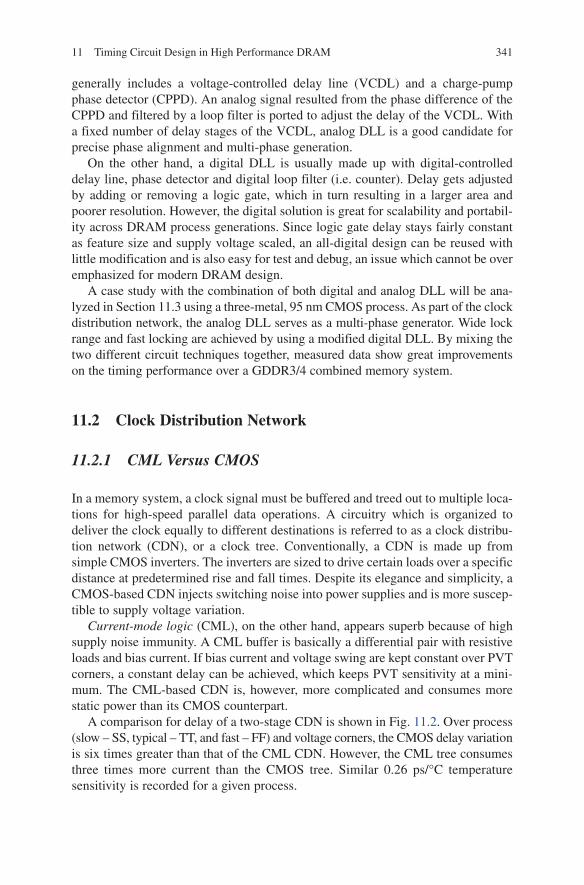
11.2.2 Clock Division and Multiphase Clocking
In order to improve signal quality and reduce jitter and ISI for high-speed clock distribution, a clock divider is generally applied to slow down the internal clock speed. To maintain double-data rate operation, both rising and falling edges of the full speed clock must be counted for multiphase clocking after division, which results in two pairs of differential half-speed clocks, one originated from the CK, the other from the CK#. Depicted in Fig. 11.3a, total 4 bits of data are clocked at each rising edge of the four 90-degree phase-shifted clocks, C0, C90, C180 and C270. The clocks generated by two clock dividers run at a quarter of the data rate. For 4-Gb/s data rate, the internal divided clocks operate at only 1 GHz. This tech-nique greatly improves the achievable speed for an existing DRAM process. Use of multiphase ¼ rate clocks subsequently simplifies design of the capture latches and deserializers due to the relaxed clock speed.
One drawback to including a CMOS divider in the critical timing path is increased voltage sensitivity (remember a
CMOS » 1 from the previous example).
Therefore, a CML latch based divider, shown in Fig. 11.3b, is instead used in this design. The CK and CK# are the differential full-speed clocks, and Nbias is the CML bias voltage. The half speed differential outputs, Out and Out# are fed back to the inputs of the divider. Two CML latches are configured as a master and slave for each divider. While the added CML divider helps to reduce voltage sensitivity for the CDN, it still produces higher temperature sensitivity, which must be mitigated.
11.2.3 Voltage and Temperature Insensitive CDN
By combining both CML and CMOS circuits, a mixed-mode, voltage and tempera-ture insensitive CDN topology is depicted in Fig. 11.4. The clock receiver (Rx) is a CML based differential receiver with hooks for duty-cycle correction (DCC). The outputs of the Rx are fed into a CML divider (Fig. 11.3) for 4-phase ¼ rate clock generation. After conversion from CML to CMOS (via c2c), the 4-phase clocks are distributed through CMOS inverters to data capture latches and deserializers. Four copies of this CMOS tree (only one is shown in Fig. 11.4) are matched to deliver the 90-degree phase shifted ¼ rate clocks to 16 different locations.
With a conventional 2-phase CML CDN (CK and CK# running full speed all the way through the CDN), there is no divider in the data capture path (most critical timing path) and the global routes are driven by CML buffers. Only two copies of the local CMOS trees running full speed are needed to drive the data capture latches. However, after data capturing, there is still a need for a clock divider and an additional 4-phase clock tree for subsequent deserialization (data stream is dese-rialized from 2-bit into 4-bit). Simulations were run to measure average current for
Local CMOSTree for 4 DQs
Local CMOSTree for 4 DQs
Local CMOSTree for 4 DQs
300um
c2c
RxCMLDiv
Clocks 4-phase CML
4-phase CMOS
2-phase CML
2DQs 2DQs
120um 120um
GS1
GS2 GS2
Fig. 11.4 A mixed-mode 4-phase CDN with 16 DQs
34511 Timing Circuit Design in High Performance DRAM
both of the described configurations at 4-Gb/s, 1.35 V, 85°C and a typical process corner. The 2-phase CML CDN produced the shortest delay at 252 ps versus 372 ps for the 4-phase mixed-mode CDN. Average current is 30 and 10 mA for the 2-phase CML and the proposed 4-phase CDN, respectively.
As mentioned before, we try to minimize VT sensitivity in the CDN to avoid the need for either retraining or on-die timing circuits, i.e., DLL. By mixing CML and CMOS circuits in the proposed CDN, we reduce supply sensitivity while minimiz-ing power consumption. However, temperature behavior is degraded because of the CML divider. Since CML and CMOS buffers have similar positive temperature coefficients (0.26 ps/°C from the previous example), what opportunity is there to improve the temperature sensitivity?
Let’s first look at how we generate the bias voltage (e.g., Nbias in Fig. 11.3b) for the CML circuits. To achieve a near constant delay, Nbias must be adjusted to provide constant current (I
tail) within the CML elements. With a constant current
flowing through the load resistor (RL), as shown in Fig. 11.3b, the output swing of
the CML also remains constant. The propagation delay (t) of a CML buffer can be defined as
* * /L tailC R C V It = D= (11.2)
where the C is the load capacitance and DV is the output swing. Notice the delay has no direct relationship to the supply voltage.
Generation of a constant current reference across different voltages and tempera-tures is best accomplished using Bandgap Reference (BGR) based circuitry. An example configuration is shown in Fig. 11.5 that employs a simple current mirror and diode load referenced to a BGR. The resulting Vinit exhibits a negative temperature coefficient that tracks threshold voltage behavior over temperature. To cancel the positive temperature coefficient evident in the CMOS buffers, we explored using the fixed bias voltage scenario depicted in Fig. 11.5. A resistor (R
L)
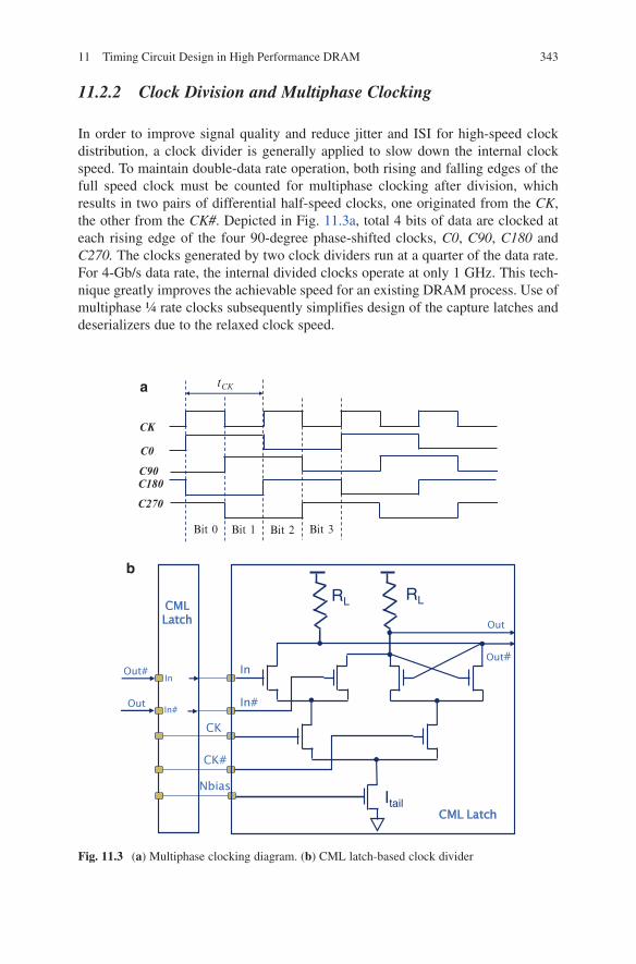
serves as the current mirror load for fixed bias generation. For a given process, a fixed bias voltage (VA) can be selected and applied to the CML circuits. The fixed biasing scheme makes the CML circuit experiencing a negative temperature coefficient (the t is reduced as the temperature goes up), which, combined with a positive temperature response from the CMOS tree, resulting a net flat temperature response for the overall design. A plot of temperature sensitivity across three
BandgapReference
Vinit
BandgapReference
VA
Fixedbias
Fixedswing
I
RL
Fig. 11.5 CML bias generation: fixed-swing versus fixed-bias
346 F. Lin
different processes (SS, TT and FF) for the proposed 4-phase CDN is shown in Fig. 11.6. Overall, a 70% reduction in temperature sensitivity was achieved through the use of fixed bias voltages. However, there is only a merely 6% increase in power at 100C and typical corner with the new bias scheme.
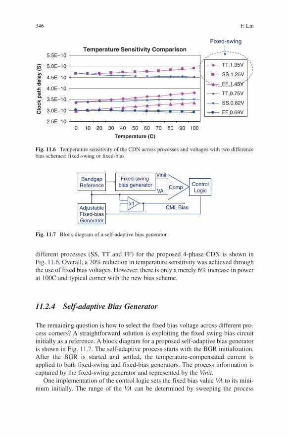
11.2.4 Self-adaptive Bias Generator
The remaining question is how to select the fixed bias voltage across different pro-cess corners? A straightforward solution is exploiting the fixed swing bias circuit initially as a reference. A block diagram for a proposed self-adaptive bias generator is shown in Fig. 11.7. The self-adaptive process starts with the BGR initialization. After the BGR is started and settled, the temperature-compensated current is applied to both fixed-swing and fixed-bias generators. The process information is captured by the fixed-swing generator and represented by the Vinit.
One implementation of the control logic sets the fixed bias value VA to its mini-mum initially. The range of the VA can be determined by sweeping the process
Temperature Sensitivity Comparison
2.5E−10
3.0E−10
3.5E−10
4.0E−10
4.5E−10
5.0E−10
5.5E−10
0 10 20 30 40 50 60 70 80 90 100
Temperature (C)
Clo
ck p
ath
del
ay (
S) TT,1.35V
SS,1.25V
FF,1.45V
TT,0.75V
SS,0.82V
FF,0.69V
Fixed-swing
Fig. 11.6 Temperature sensitivity of the CDN across processes and voltages with two difference bias schemes: fixed-swing or fixed-bias
BandgapReference
Fixed-swing bias generator
AdjustableFixed-biasGenerator
CompVA
Vinit
ControlLogic
x1CML Bias
Fig. 11.7 Block diagram of a self-adaptive bias generator
34711 Timing Circuit Design in High Performance DRAM
corners. After comparing Vinit and VA via a comparator, the results are fed into the control logic to determine if the VA needs to be adjusted for the process or not. When the VA is greater than the Vinit, the calibrating process is completed. A unit gain buffer is inserted between the VA and the final CML bias voltage. The fixed-swing generator, comparator, and control logic can be idled or shut off to save power after the calibration.
For a given device on a given process, the calibration only needs to be run once during the power-up initialization. Three-bit binary weighted current sources are used for adjustment (Fig. 11.5). A 3-bit UP counter selects the value of the current. The step size is around 20 mV with a 10 kΩ resistor. The calibration takes a couple hundred cycles, depending on the process corner and clock frequency. Calibration can be part of the power-up sequence.
11.2.5 Simulation Results
Simulation results based upon the proposed CDN are summarized in Tables 11.1 and 11.2. Both results for the fixed-swing and fixed-bias generators are listed for comparison. The mixed-mode CDN shown in Fig. 11.4 was targeted with different biasing schemes. Using typical models (TT) from a 3-metal 50 nm DRAM process, the fixed bias is set around 0.77 V, where the CML bias for the fixed-swing genera-tor can vary between 0.71 and 0.78 V. The timing improvement over a 100 mV and 85°C VT change is about 40%. For a temperature change only at 1.45 V, from Table 11.2, a 68% improvement is achieved. Compared to the 2-phase CML CDN described before, the proposed 4-phase CDN approaches a similar timing performance over the voltage and temperature variations while at the same time, consumes far less power and simplifies the timing path design (with only one CDN and consolidated data capture and deserialization).
For low-voltage operations, the improvement using the proposed VT insensitive CDN is not as significant as that at higher voltages. At 1.35 V, only 45% improve-ment is recorded over 85°C temperature change, as compared to 68% at 1.45 V. For low-voltage high-speed memory applications, voltage sensitivity is dominant factor for the timing budget. A clock distribution design with more CML components may be more appropriate in this case.
Table 11.1 Simulation results across voltage and temperature
TT, 4 GpbsPropagation delay of the clock distribution networkVoltage, Temperature Fixed-swing (ps) Fixed-bias (ps)
Clock synchronization circuit (CSC) is another critical timing circuitry related to high performance DRAM. As the clock speed for I/O interfaces push well into the gigahertz range, designing CSC, or de-skewing circuitry, becomes a challenge. The on-die sync circuit must cover a wide operation range and, at the same time, achieve good jitter performance. Inclusion of on-die clock synchronization is necessary for control of output timing skew between the system clock and the output data from the DRAM. However, there are side effects from the use of sync circuits when the system clock period becomes comparable with the I/O delay of the DRAM. Variations in process, voltage, and temperature (PVT) can easily cross cycle boundaries and make read latency (i.e. CL) prediction difficult. Besides latency control, high-speed clock distribution is also susceptible to duty-cycle distortion, power supply noise, and timing mismatch. Power and jitter for timing circuits must be carefully gauged to achieve overall better performance.
From all-digital approach [7–8] to pure analog implementation, from open-loop synchronous mirror delay (SMD) [10] to close-loop architecture, there are various flavors in designing a sync circuit based on different applications [4–15]. Traditionally, a delay-locked loop (DLL) is selected for memory interfaces due to its close-loop architecture and relatively simple implementations. In this section, we will explore a mixed-mode DLL (MDLL) used in a combination 512 Mb 2.0 Gb/s/pin GDDR3 and 2.5 Gb/s/pin GDDR4 synchronous DRAM. The chip was fabricated in a 1.5 V 95 nm triple-metal CMOS process. The measured maximum achievable clock frequency is 2 GHz at 2.12 V supply.
11.3.1 MDLL Clocking Architecture
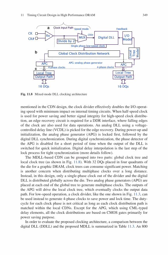
The proposed mixed-mode DLL (MDLL) [2] clocking system is shown in Fig. 11.8. A conventional digital DLL with fast-lock and fine resolution (via phase interpola-tion) is adopted for clock synchronization and de-skewing. A clock divide-by-2 circuit is inserted into the input path to slow down the internal clock speed for high-speed GDDR4 operation. To extend the lock range of the MDLL, a MUX is either used to select full-speed (i.e. GDDR3) or half-speed (i.e. GDDR4) clock. As
Table 11.2 Simulation results across temperature
TT, 4 GpbsPropagation delay of the clock distribution networkVoltage, Temperature Fixed-swing (ps) Fixed-bias (ps)
34911 Timing Circuit Design in High Performance DRAM
mentioned in the CDN design, the clock divider effectively doubles the I/O operat-ing speed with minimum impact on internal timing circuits. When half-speed clock is used for power saving and better signal integrity for high-speed clock distribu-tion, an edge recovery circuit is required for a DDR interface, where falling edges of the clock are also used for data operations. An analog DLL using a voltage-controlled delay line (VCDL) is picked for the edge recovery. During power-up and initialization, the analog phase generator (APG) is locked first, followed by the digital DLL synchronization. During digital synchronization, the phase detector of the APG is disabled for a short period of time when the output of the DLL is switched for quick initialization. Digital delay interpolation is the last step of the lock process for tight synchronization (more details follow).
The MDLL-based CDN can be grouped into two parts: global clock tree and local clock tree (as shown in Fig. 11.8). With 32 DQs placed in four quadrants of the die for a graphic DRAM, clock trees can consume significant power. Matching is another concern when distributing multiphase clocks over a long distance. Instead, in this design, only a single-phase clock out of the divider and the digital DLL is distributed globally across the die. Two analog phase generators (APG) are placed at each end of the global tree to generate multiphase clocks. The outputs of the APG will drive the local clock tree, which eventually clocks the output data path. For low-speed operation, a clock divider, like the one shown in Fig. 11.3, can be used instead to generate 4-phase clocks to save power and lock time. The duty-cycle for each clock phase is not critical as long as each clock distribution path is matched within the local CDNs. Except for the APG, which using CML-typed delay elements, all the clock distributions are based on CMOS gates primarily for power saving purpose.
In order to evaluate the proposed clocking architecture, a comparison between the digital DLL (DDLL) and the proposed MDLL is summarized in Table 11.3. An 800
Rx
Divide by 2MUX Digital DLL
Global Clock Distribution Network
APG
Local TreeOutput Path
16 DQs
CK
CK#
4-phase clocksAPG
Local TreeOutput Path
16 DQs
4-phase clocks
Single phase low-speed clock
I/O Model
Loca
l T
ree
Mod
el
Speed mode Feedback
CKIn
APG: analog phase generator
Clock Input Patha
b
c
Fig. 11.8 Mixed-mode DLL clocking architecture
350 F. Lin
MHz external clock is fed into both DLLs. The clock is running at full speed for the DDLL and half speed for the MDLL. Four-phase clocks are generated by a clock divider for the DDLL and an APG for the MDLL, respectively. Simulation is per-formed at 1.5 V, typical process and 85°C. Duty-cycle correction (DCC) for the DDLL is not included in this simulation, which requires additional power, area, and lock time for the conventional approach. From Table 11.3, the proposed MDLL consumed less power for both DLL and global clock tree (including two APGs) due to half-speed clocking. However, the lock time did increase for analog phase generation.
11.3.2 Fast-Lock Digital DLL
The digital DLL used in the MDLL can achieve fast lock with a measure-controlled delay (MCD) line, shown in Fig. 11.9a. The time-to-digital conversion (TDC) and digital-to-time conversion (DTC) will start during measure initialization. The input delay (t
in) and output delay (t
out) are modeled with an I/O model (t
in + t
out). Delay for
clock distribution is tTree
in Fig. 11.9a. The intrinsic loop delay (tILD
) is defined as
ILD Tree in outt t t t= + + (11.3)
The tILD
is measured by the measure delay array (MDA) and the difference (N*t
CK − t
ILD) is stored in the forward delay array (FDA). Parameter t
CK is the clock
period and N is an integer number. When tCK
> tILD
, N = 1.During initial measurement, the FDA is bypassed by the two-input MUX. A
Start signal triggered by the rising edge of the internal clock (CKIn) initializes the measurement. As shown in Fig. 11.9, the Start signal propagates through the clock tree and I/O model and becomes the Stop signal at the input of the MDA. The time difference between the two signals (Start and Stop) is t
ILD. The outputs of the MDA
are sampled by the CKIn and the output digital codes are stored in the Measure Control block. After the difference between N*t
CK and t
ILD is captured and reflected
in the FDA, the initialization is completed and the loop is locked (total delay from external to output clock is N*t
CK). An example timing diagram with N = 2 is
depicted in Fig. 11.9b. The delay gets adjusted by adding or removing delay stages. Assuming the delay per stage is t
D, the number (n) of delay stages picked after the
MCD initialization is approximately
( * ) / 1CK ILD Dn N t t t= - ± (11.4)
Table 11.3 Comparison between conventional digital DLL (DDLL) and proposed mixed-mode DLL (MDLL) at 1.5 V, 85°C, and 800 MHz external clock
DLL current (mA)
Global clock tree + phase generator (mA)
Local clock trees (mA) Lock time (ns)
DDLL 14 13.3 50 56MDLL 8.2 13.1 50 146
35111 Timing Circuit Design in High Performance DRAM
After the measurement, the output of the FDA is selected and normal DLL loop is resumed thereafter for voltage and temperature tracking. Because MDA and FDA are identical and operating mutual exclusively, the MDA and FDA can be combined to save area. Typical digital delay for two logic gates (t
D) is around 100–150 ps.
Typical lock time for the MCD-based DLL is around ten clock cycles.A digital delay interpolation (DDI) [15] or mixing out of one FDA element is
followed to achieve better resolution, generally in 5–15 ps range. Typical lock time for the entire DDLL is less than 60 cycles, depending on clock frequency, intrinsic loop delay, adjustment rate, and final resolution. Compared to the two-cycle lock of a conventional synchronous mirror delay (SMD) [10] or clock-synchronized delay (CSD), the lock time is longer for the MCD because of switching the output via the
Fig. 11.9 (a) Fast-lock, measure-controlled delay (MCD) based digital DLL. (b) Timing diagram of the MCD operation (N = 2)
tin Forward Delay ArrayCK
CK#MUX
Measure Control (Latch)
Measure Delay Array
Phase Detector & Control
I/O Model (tin + tout)
Clock Distribution (tTree)tout
Output Clock
Switch is closedonly during
Measureinitialization
Upper path is selected during Measure Init
TDC
DTC
Stop
StartCKIn
N * tCK -(tTree + tin + tout)
N * tCK -(tTree + tin + tout) a
CKIn
Start
Stop
tCK
tILD 2*tCK-tILD
MDA Stop
Measure Control…
CKIn
Digital codes (…1111111100000…)
FDA
b
352 F. Lin
MUX. Longer delay through the digital loop, clock path and I/O model with regard-ing to a shorter t
CK also requires extra time for the feedback signal to settle. Finer
resolution achieved by subsequent delay interpolation further increases the lock time. The data quoted in Table 11.3 shows a lock time about 45 cycles for the DDLL, which is significantly better than the 200-cycle spec requirement. Even with the analog DLL, the lock time is still within the spec. Although the finer adjustment circuitry can be designed using an analog approach, an all-digital imple-mentation is still adopted in the clock architecture for its simplicity, scalability, and fast lock time.
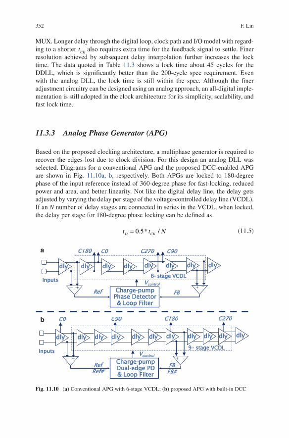
11.3.3 Analog Phase Generator (APG)
Based on the proposed clocking architecture, a multiphase generator is required to recover the edges lost due to clock division. For this design an analog DLL was selected. Diagrams for a conventional APG and the proposed DCC-enabled APG are shown in Fig. 11.10a, b, respectively. Both APGs are locked to 180-degree phase of the input reference instead of 360-degree phase for fast-locking, reduced power and area, and better linearity. Not like the digital delay line, the delay gets adjusted by varying the delay per stage of the voltage-controlled delay line (VCDL). If an N number of delay stages are connected in series in the VCDL, when locked, the delay per stage for 180-degree phase locking can be defined as
0.5* /D CKt t N= (11.5)
dly dly dly dly dly dly dly dly
C0 C90
6- stage VCDL
Charge-pumpPhase Detector& Loop Filter
VcontrolInputs
Ref FB
dly dly dly dly dly dly dly dly
C0 C90
9 - stage VCDL
Charge-pumpDual-edge PD& Loop Filter
C180 C270
VcontrolInputs
RefRef#
FBFB#
dly dly dly
C180 C270a
b
Fig. 11.10 (a) Conventional APG with 6-stage VCDL; (b) proposed APG with built-in DCC
35311 Timing Circuit Design in High Performance DRAM
For 800 MHz clock and 6-stage VCDL shown in Fig. 11.10a, the analog delay per stage is around 104 ps when the APG is locked. Compared to digital adjust-ment, analog VCDL is quite different with a fixed number of delay stages and generally smaller layout area to cover the full operating range. Built with differen-tial CML logic, the analog delay line has much less intrinsic delay and better supply noise rejection capability (a
VCDL close to 0.5 with a CML to CMOS converter). To
maintain similar characteristics of the analog delay, the length (N) of the VCDL needs to be doubled to 12 when a 360-degree phase locking is selected.
One drawback for 180-degree locking is sensitivity to input duty-cycle distortion (DCD). Because the falling edge of the input signal is used to generate feedback for the phase detector (PD), any input DCD will cause a misalignment for the multiphase outputs. For the proposed MDLL-based CDN, the DCD is likely generated from the DDLL and global clock distribution network. A separated duty-cycle correction circuit is generally required in the conventional APG for high-speed operation.
Instead of using complementary phases, such as clock 180 and 270 in Fig. 11.10a, the proposed APG adds extra three delay stages to form a 9-stage VCDL. Multiple phases are tapped off from the equal length delay stages of the VCDL, as shown in Fig. 11.10b. The dependency of output DCD due to input duty-cycle is removed with the proposed configuration. However, output DCD depen-dency still needs to be solved for the feedback signal (FB), which is generated by using the falling clock edges.
A fully differential dual-edge phase detector (DDPD) can be used to perform automatic DCC, as is shown in Fig. 11.11a. Inputs Ref and Ref# are differential references, while FB and FB# are differential feedback signals. Based on transi-tions of both rising and falling edges, pulses are generated to trigger the SR latches and create UP and DN signals, respectively. Timing diagrams for this DDPD are shown in Fig. 11.11b with only UP and DN signals for clarity. Whenever both UP and DN are in the same state, either ‘1’ or ‘0’, there is no net charge dumped into the loop filter, and the control voltage (V
control) remains unchanged. During normal
phase locking, Vcontrol
gets adjusted twice – one at rising edges and one at falling edges. With input duty-cycle distortion (DCD) present, the relationship is plotted in Fig. 11.11b with equal intervals for pumping up and down when locked. The aver-age impact on V
control is zero and the loop is locked. With 1 GHz external clock and
46% duty-cycle internal clock (2 ns period), simulation data shows that the pro-posed APG maintains the desired phase alignment (500 ps apart from each other) while the conventional APG produced a worst-case bit time of 403 ps (40% duty cycle relative to the external clock as, measured between the four phases).
A self-bias VCDL [17] is used for the proposed APG. The VCDL is clamped to its minimum delay initially to avoid false locking. A fully differential current steer-ing charge pump phase detector (CPPD) [18] is used to generate the control voltage for the VCDL with no dead zone. The typical lock time for the APG is in the order of 100 cycles. The analog implementation including all decoupling capacitors occupies roughly 133 × 317um2, which is one third of the size of the DDLL. Average current drawn from the APG is around 3–5 mA depending on the fre-quency and operating conditions.
354 F. Lin
11.3.4 Measurement Results
Using the proposed mixed-mode DLL, an 88 mm2 512 Mb × 32 GDDR3/GDDR4 device, is fabricated in a 1.5 V 3-metal 95 nm CMOS process. Figure 11.12a is a measured t
CK-VDD Shmoo data showing device performance reaching beyond 2
Gbps/pin in GDDR3 operation for page fast write and read vectors that produce 2 ns column cycle times (data failure limited). The CAS latency (CL) is 12 with a burst length (BL) of 4 for the GDDR3 operation. Figure 11.12b is a measured jitter histogram of read strobe (RDQS), where the part is running at 1.5V, 1 GHz in GDDR4 mode. The RMS jitter and the peak-to-peak jitter are 4.63 and 38 ps, respectively. Performance results are summarized in Table 11.4.
Fig. 11.11 (a) Fully differential dual-edge phase detector (DDPD). (b) Timing diagrams of a dual-edge phase detector (locking w/o DCD in the left and locked w/ DCD in the right)
FB
Ref# DN
DN#
Differential Dual- Edge Phase Detector
Ref
FB# UP
UP#
SR Latch
a
FB
Ref
UP
DN Pump Up at both edges
FB
Ref
UP
DN
Pump Up Pump Down
b
35511 Timing Circuit Design in High Performance DRAM
Fig. 11.12 (a) tCK vs. VDD Schmoo GDDR3, BL = 4, temperature = 25/85°C, CL = 12. (b) Measured jitter histogram at 1 GHz, 1.5 V and GDDR4
356 F. Lin
The RDQS is treated as a special data (DQs) with a ‘0101’ toggling pattern. A Read strobe is bundled with 8-bit of data and forwarded back to memory control-lers for data capture. The timing spec for the RDQS and DQs (i.e. t
DQSQ) is much
tighter than the one for the system clock (e.g. CK) and DQs (i.e. tAC
). A typical tDQSQ
is limited to only 80 ps for a GDDR4 operation and the skew is mainly due to mismatches from the CDN and channel links. The t
AC spec, on the other hand, is
proportional to tCK
(e.g. 0.25*tCK
or 200 ps for 2.5 Gb/s data rate) and dictated by I/O modeling and sync circuit performance. The forwarded strobes keep the mem-ory interface source synchronous and facilitate high-speed data operation. The data rate can be extended well beyond 2.5 Gbps by using the proposed half-speed clock-ing and mixed-mode DLL.
11.3.5 Other Consideration
Compared to a traditional digital DLL, the mixed-mode DLL (MDLL) is a step forward in both operating speed and lock range. However, the MDLL may not be suit-able for the input timing adjust due to its overall longer delay path, which is more susceptible to voltage and temperature (VT) variations. If on-die VT tracking and de-skewing via a sync circuit is desire for the input path, like the one shown in Fig. 11.4, circuit modifications are necessary to further improve the timing performance.
Let’s first revisit the clocking architecture shown in Fig. 11.8. Assuming a differ-ential CML receiver (Rx) for the system clock, there are at least three places (dotted lines) in Fig. 11.8 where CML to CMOS or CMOS to CML conversion takes place:
(a) from the CML Rx to the CMOS input (CKIn)(b) from single-phase CMOS output of the global CDN to CML inputs of the APG(c) from the VCDL of the APG to 4-phase CMOS clocks fed to local trees
Each logic conversion adds delay and impacts overall timing. A straightforward upgrade is to get rid of the logic conversion as much as you can and change circuits between (a) and (b) into CML-based logic. A CML-typed clock divider (shown in Fig. 11.3b) and CML-based MUX can be used instead for the clock input path. An analog DLL (ADLL), like the one shown in Fig. 11.10a can be adopted for clock synchronization. Duty-cycle distortion may not be an issue due to fully differential CML operation through the clock input path. The 6-stage VCDL in Fig. 11.10a can provide 12 phases with a 30° phase shift for analog phase interpolation (API) [9].
Table 11.4 Performance summary of the proposed MDLL
Technology 3-metal 95 nm CMOS process
Supply voltage 1.5–1.8 V nominalOperating frequency 400–1,250 MHzJitter at 1.5 V, 1 GHz, GDDR4 38 ps (peak-to-peak), 4.63 ps (RMS)Lock time <200 clock cyclesMaximum speed 4 Gb/s/pin at 2.12 V supply
35711 Timing Circuit Design in High Performance DRAM
An exemplary 15-bit thermometer code can be applied to interpolate between any two adjacent phases. The final resolution after interpolation is about two degree (or about 7–10 ps for an internal speed of 800 MHz).
The locking procedure for the ADLL can be divided into three steps. The first step is to lock the delay of the VCDL to half of the clock period (i.e. 0.5 * t
CK). As
shown in Fig. 11.10a, the charge-pump phase detector (CPPD) and the loop filter will adjust the control voltage (V
control) until the feedback (FB) and reference (Ref)
are in sync. The initial Vcontrol
can be clamped to achieve a minimum delay in the VCDL. If a similar analog delay is replicated in the analog phase generator (APG), the control voltage (V
control) from the ADLL can be ported to bias the 9-stage VCDL
of the APGs. Therefore, even without enabling its own CPPD, the APG can acquire lock at the same time when the ADLL is locked. Matching the various VCDLs (Fig. 11.10a, b) in both loading and interconnects makes it easy to consolidate the initial locking steps and reduce overall lock time.
After the ADLL is locked, the dual-edge CPPD (Fig. 11.11) of the APG is enabled for duty-cycle adjustment and further polish for its tight locking. The final step is analog phase interpolation (API) [19] between two adjacent phases out of the VCDL of the ADLL. Instead of using a charge-pump circuitry, a separate phase detector (PD) with window detection and digital filtering can be applied for phase selection and interpolation. Just like digital DLL, the added window detection and digital filtering can further improve the jitter performance of the API. Any jitter coupled from the I/O model and presented at the input of the PD via the feedback signal can be tracked and filtered before any adjustment. The digital codes won’t be changed until the phase error is beyond a predetermined window (e.g. 20 ps). The resulted digital codes for the API can be stored in a shift register or an up-down counter. Similar interpolation control logic makes the transition from digital DLL to analog DLL a lot easier for design, test and debug. The learning curve is not as steep when similar circuit blocks (e.g. the APG and the digital logic) have been scrutinized and investigated before in the MDLL.
Besides the sync circuits and clock input path, the global clock tree can also be upgraded to CML based CDN (2-phase ¼ rate), which eliminating the interface (b) between the global CDN and APGs. Although the ADLL and APG can be further consolidated into one with multiple APIs, the power consumption over a 4-phase global CML CDN may not justify the modification.
The last piece of the clock path stays the same with a local CMOS clock tree to deliver the 4-phase ¼ rate CMOS clocks to the output path. The techniques discussed in the Section 11.2 for a voltage and temperature insensitive CDN can also be applied here. The CML-based clock input path and the global CDN are biased by a fixed voltage, with process information calibrated by a self-adaptive bias generator (Fig. 11.7). The power out of the global CDN can be further scaled down according to the operating frequency, which can be monitored by the ADLL.
Instead of using current-mode logic, another way to mitigate the power supply sensitivity is by supply regulation. The internal power supplies for the critical tim-ing circuits can be regulated and isolated from the rest of the periphery circuits. Based on the Eq. 11.1, the a factor gets bigger at lower voltages, therefore, supply
358 F. Lin
regulation may not be a good candidate to solve timing problem as the feature size and supply voltage keep scaling down. For example, the typical supply voltage (VDD) for the 95 nm DRAM process is 1.5 V (GDDR4) or 1.8 V (GDDR3), but the VDD for the 50 nm process is only 1.35 V. There are not enough margins left for voltage regulation as the process scaled into deep submicron region. Dedicated power supply pins and good on-die power delivery for the timing circuits are a few keys to keep timing specs on check.
11.4 Future Directions for Nanoscaled DRAM Interface
High-performance computing system, such as multi-core processor or high-end game console, continues to advance and demands higher bandwidth and lower power from the DRAM. These demands directly impact the DRAM interface protocol and hence, the timing circuit design. At the same time, cutting throat com-petition in the commodity DRAM market forces DRAM manufacturers pushing down the cost and chasing the endless process scaling. The bleeding edge technolo-gies create a slew of challenges, not necessary new but in a different scale, facing to today’s DRAM designer, such as density, I/O transfer rate, power consumption and device variability. Given the historical trends, the future for the nanoscaled DRAM interface should continue to grow in speed, burn more power, and operate at lower supply voltages. But these trends may not be sustainable due to cost and power concerns. Instead of a skyrocket clock frequency, like the race in the micro-processor world a few years back, a course change (just like from single-core to multi-core change in the microprocessor) is necessary to fuel a higher performance DRAM with a reasonable power and cost structure. It is hard to predict what those changes are, but hopefully from the selective topics in this chapter, the reader will appreciate of the difficulties we are encountering and maybe get an idea for poten-tial solutions to problems related to DRAM interfaces.
Moving forward, there are other areas of consideration for high-performance DRAM that may impact timing circuit design. One area only briefly mentioned in this chapter is link initialization for high-speed data operations. Link initialization conducted by memory controller via extensive training may be beneficial to offload some of the burden of the timing circuit design from the DRAM. Per-pin deskewing [16] looks promising but adds a lot of complexity and overhead in the memory con-troller. The link initialization may also add a significant test and debug time to vali-date a memory interface.
Another possibility is moving the timing circuits and high-speed I/O into an intermediate chip, like the advanced memory buffer (AMB) used in fully-buffered dual in-line memory module (FB-DIMM). The AMB, fabricated with logic pro-cesses, serves as an intermediate buffer between memory controller and DRAM devices. A narrow point-to-point channel supported by the AMB enables high-speed communication between the host controller and AMB. At the same time, a wide channel between the AMB and memory devices provides higher bandwidth.
35911 Timing Circuit Design in High Performance DRAM
The additional latency and cost resulted from the intermediate chip may or may not be justified by the improved performance.
A radical change recently for high density DRAM devices is by 3-dimensional integration (3-DI), which stacking memory devices vertically using through-silicon vias (TSVs). Aside from the existing chip-stacking technologies, such as wire-bonding, flip-chip, multichip packaging (MCP) and system-in-package (SiP), the TSV technique explores the chip-stacking and interconnecting vertically by deploy-ing TSVs. An 8-gigabit 3D DDR3 DRAM based on 50 nm technology [20] has been reported with a single master device and three slave chips connected using 300 TSVs. The pitch of the TSVs is only 60-µm. The master device acts as a buffer that isolates the channel and the slave chips. The timing circuits are located only in the master device, which in turn, saves power compared to conventional quad-die package structures. The prototype device also utilizes a separate datapath (a bidi-rectional local datapath and unidirectional global datapath – read/write separated), a modified repair scheme and a power-noise reduction technology.
The TSV technology opens a door for continuous circuit innovations in array architecture, signaling, timing control, error detection and correction, redundant and repair algorithm, and test and debug. Although there is still a lot challenges ahead with the new technology, by shortening the interconnections between the chips, it’s not hard to envision a next generation memory system emerged with reduced power and die size, improved timing and elevated bandwidths.
References
1. B. Keeth, R.J. Baker, B. Johnson, F. Lin, DRAM Circuit Design – Fundamental and High-Speed Topics (Wiley-IEEE Press, Piscataway, NJ, 2007)
2. F. Lin, R. Royer, B. Johnson, B. Keeth, A wide-range mixed-mode DLL for a combination 512 Mb 2.0 Gb/s/pin GDDR3 and 2.5 Gb/s/pin GDDR4 SDRAM. IEEE J. Solid-St. Circ. 43(3), 631–641 (2008)
3. I.E. Sutherland, R.F. Sproull, D. Harris, Logical Effort: Designing Fast CMOS Circuits (Academic, San Diego, CA, 1999)
4. S. Bae, Y. Sohn, K. Park, K. Kim, D. Chung, J. Kim, S. Kim, M. Park, J. Lee, S. Bang, H. Lee, I. Park, J. Kim, D. Kim, H. Kim, Y. Shin, C. Park, G. Moon, K. Yeom, K. Kim, J. Lee, H. Yang, S. Jang, J. Choi, Y. Jun, K. Kim, A 60nm 6Gb/s/pin GDDR5 graphics DRAM with multifaceted clocking and ISI/SSN-reduction techniques, in IEEE ISSCC Dig. Tech. Papers, 278–279 (2008)
5. K. Lee, J. Cho, B. Choi, G. Lee, H. Jung, W. Lee, K. Park, Y. Joo, J. Cha, Y. Choi, P.B. Moran, J. Ahn, A 1.5-V 3.2 Gb/s/pin Graphic DDR4 SDRAM with dual-clock system, four-phase input strobing, and low-jitter fully analog DLL. IEEE J. Solid-St. Circ. 42(11), 2369–2377 (Nov. 2007)
6. F. Lin, B. Keeth, A Self-Adaptive and PVT Insensitive Clock Distribution Network Design for High-Speed Memory Interfaces. Proceedings of the IEEE/EDS Workshop on Microelectronics and Electron Devices (WMED) (2009), pp. 55–58, Boise, ID
7. F. Lin, J. Miller, A. Schoenfeld, M. Ma, R.J. Baker, A register-controlled symmetrical DLL for double-data-rate DRAM. IEEE J. Solid-St. Circ. 34(4), 565–568 (1999)
8. T. Matano, Y. Takai, T. Takahashi, Y. Sakito, I. Fujii, Y. Takaishi, H. Fujisawa, S. Kubouchi, S. Narui, K. Arai, M. Morino, M. Nakamura, S. Miyatake, T. Sekiguchi, K. Koyama, A
360 F. Lin
1-Gb/s/pin 512-Mb DDRII SDRAM using a digital DLL and a slew-rate-controlled output buffer. IEEE J. Solid-St. Circ. 38(5), 762–768 (2003)
9. S. Sidiropoulos, M.A. Horowitz, A semi-digital dual delay-locked loop. IEEE J. of Solid-St. Circ. 32(11), 1683–1692 (1997)
10. T. Saeki, Y. Nakaoka, M. Fujita, A. Tanaka, K. Nagata, K. Sakakibara, T. Matano, Y. Hoshino, K. Miyano, S. Isa, S. Nakazawa, E. Kakehashi, J.M. Drynan, M. Komuro, T. Fukase, H. Iwasaki, M. Takenaka, J. Sekine, M. Igeta, N. Nakanishi, T. Itani, K. Yoshida, H. Yoshino, S. Hashimoto, T. Yoshii, M. Ichinose, T. Imura, M. Uziie, S. Kikuchi, K. Koyama, Y. Fukuzo, T. Okuda, A 2.5-ns clock access, 250-MHz, 256-Mb SDRAM with synchronous mirror delay. IEEE J. Solid-St. Circ. 31, 1656–1665 (1996)
11. Y. Jung, S. Lee, D. Shim, W. Kim, C. Kim, S. Cho, A dual-loop delay-locked loop using multiple voltage-controlled delay lines. IEEE J. Solid-St. Circ. 36(5), 784–791 (2001)
12. J. Kim, S. Lee, T. Jung, C. Kim, S. Cho, B. Kim, A low-jitter mixed-mode DLL for high-speed DRAM applications. IEEE J. Solid-St. Circ. 35(10), 1430–1436 (2000)
13. G. Dehng, J. Lin, S. Liu, A fast-lock mixed-mode DLL using a 2-b SAR algorithm. IEEE J. of Solid-St. Circ. 35(10), 1464–1471 (2001)
14. B. Johnson, B. Keeth, F. Lin, H. Zheng, Phase-tolerant latency control for a combination 512Mb 2.0gb/s/pin GDDR3 and 2.5gb/s/pin GDDR4 SDRAM. ISSCC 2007 Digest of Tech. Papers, 494–495 (2007)
15. B. Garlepp, K.S. Donnelly, K. Jun, P.S. Chau, J.L. Zerbe, C. Huang, C.V. Tran, C.L. Portmann, D. Stark, Y.F. Chan, T.H. Lee, M.A. Horowitz, A portable digital DLL for high-speed CMOS interface circuits. IEEE J. Solid-St. Circ. 34(5), 632–642 (May 1999)
16. E. Yeung, M.A. Horowitz, A 2.4 Gb/s/pin Simultaneous Bidirectional Parallel Link with Per-Pin Skew Compensation, IEEE J. Solid-St. Circ. 35(11), 1619–1628 (2000)
17. J. Maneatis, Low-jitter process-independent DLL and PLL based on self-biased techniques. IEEE J. of Solid-St. Circ. 31(11), 1723–1732 (1996)
18. K. Wong, E. Fayneh, E. Knoll, R. Law, C. Lim, R. Parker, F. Wang, C. Zhao, Cascaded PLL design for a 90nm CMOS high-performance microprocessor. ISSCC Dig. Tech. Papers, 422–424 (2003)
19. B. Kim, L.S. Kim, K. Park, Y.H. Jun, S.I. Cho, A DLL with jitter reduction techniques and quadrature phase generation for DRAM interface. IEEE J. of Solid-St. Circ. 44(5), 1522–1530 (2009)
20. Uksong Kang, Hoe-Ju Chung, Seongmoo Heo, Soon-Hong Ahn, Hoon Lee, Soo-Ho Cha, Jaesung Ahn, DukMin Kwon, Jin Ho Kim, Jae-Wook Lee, Han-Sung Joo, Woo-Seop Kim, Hyun-Kyung Kim, Eun-Mi Lee, So-Ra Kim, Keum-Hee Ma, Dong-Hyun Jang, Nam-Seog Kim, Man-Sik Choi, Sae-Jang Oh, Jung-Bae Lee, Tae-Kyung Jung, Jei-Hwan Yoo, Changhyun Kim, 8Gb 3D DDR3 DRAM using through-silicon-via technology. ISSCC Dig. Tech. Papers, 130–131 (2009)