Tin assisted transfer of electroplated metal nanostructures and its application in flexible chiral metamaterials Liang Fang a , Ming Wei a , Nantakan Wongkasem b , Hamzeh Jaradat c , Anas Mokhlis c , Jia Shen a , Alkim Akyurtlu c , Kenneth Marx d , Carol Barry a , Joey Mead a,⇑ a NSF Nanoscale Science and Engineering Center for High-Rate Nanomanufacturing, Department of Plastics Engineering, University of Massachusetts Lowell, Lowell, MA 01854, USA b Department of Electrical Engineering, Khon Kaen University, Khon Kaen 40002, Thailand c Department of Electrical and Computer Engineering, University of Massachusetts Lowell, Lowell, MA 01854, USA d Center for Intelligent Biomaterials, Department of Chemistry, University of Massachusetts Lowell, Lowell, MA 01854, USA article info Article history: Received 6 August 2012 Received in revised form 15 January 2013 Accepted 7 February 2013 Available online 26 February 2013 Keywords: Flexible devices Electroplating Silver Tin Metamaterials abstract A novel method named tin-assisted transfer of nanoscale electroplated metal structures was introduced for the fabrication of flexible devices. With the addition of a tin releasing layer, electroplated metal struc- tures, which were achieved on rigid substrates using a combination of electron beam lithography and electroplating, were successfully transferred to flexible substrates. Using this method, various metal (Ag, Au, and Pt) structures were patterned onto flexible substrates. To demonstrate the utility of this pro- cess for fabrication of flexible devices, a mid-infrared flexible metamaterial with chiral structures was successfully produced. Ó 2013 Elsevier B.V. All rights reserved. 1. Introduction Flexible electronic, optical and optoelectronic devices, such as flexible circuits [1], organic field-effect transistors [2], organic light-emitting diodes [3], and flexible metamaterials [4–6], are of significant commercial interest. Compared to rigid and ultra-flat substrates, flexible polymeric substrates exhibit the advantages of flexibility, low cost, conformable manipulation, transparency, light-weight, and biocompatibility. The main requirement for fab- rication of flexible, functional devices is to pattern microscale or nanoscale metal (or other conducting) structures on flexible poly- meric substrates. There are two methods to achieve the fabrication of metal structures on flexible polymer substrates: direct patterning and indirect patterning. In direct patterning, metal structures are di- rectly patterned onto flexible polymeric substrates using a combi- nation of lithography techniques, metal depositions, and lift-off procedures. Electron-beam lithography (EBL) [4] and nanoimprint- ing [7] have been used for direct patterning of metal structures onto flexible substrates. The lift-off procedures to remove the pho- toresist, however, may cause an issue of substrate degradation due to the exposure of polymeric substrates to solvents or aqueous chemicals. Recently, Walther et al. [5] demonstrated that inkjet printing is another direct patterning method capable of creating patterned arrays of metal structures onto flexible substrates. This method was used for fabricating a flexible metamaterial [5]. The high temperature required for sintering of the printed metal nano- particles, however, may also cause degradation of polymeric substrates. The indirect patterning method consists of two separate steps. First, metal structures are deposited on a substrate using lithogra- phy (or other processes). In a second step, the metal structures are transferred to flexible substrates. Compared to direct patterning, the degradation of polymer substrates in the indirect patterning method can be overcome. To date, the only method used for indi- rect patterning is metal transfer printing [8–11], consisting of soft lithography, physical vapor deposition (PVD), and transfer. Specif- ically, a metal layer is first deposited upon a polydimethylsiloxane (PDMS) mold with surface topography. The PDMS mold is then pressed against a polymeric substrate. After a specific interval of time, only the metal layer deposited on the protruding PDMS sur- face is transferred to the polymeric substrate. Several issues should be considered in both the deposition and transfer procedures. The deposition technique in metal transfer printing is limited to PVD approaches, such as electron beam evaporation, thermal evapora- 0167-9317/$ - see front matter Ó 2013 Elsevier B.V. All rights reserved. http://dx.doi.org/10.1016/j.mee.2013.02.044 ⇑ Corresponding author. Address: NSF Nanoscale Science and Engineering Center for High-Rate Nanomanufacturing, Department of Plastics Engineering, University of Massachusetts Lowell, 1 University avenue, Lowell, MA 01854, USA. Tel.: +1 978 934 3446; fax: +1 978 458 4141. E-mail address: [email protected](J. Mead). Microelectronic Engineering 107 (2013) 42–49 Contents lists available at SciVerse ScienceDirect Microelectronic Engineering journal homepage: www.elsevier.com/locate/mee
Transcript
Microelectronic Engineering 107 (2013) 42–49
Contents lists available at SciVerse ScienceDirect
Microelectronic Engineering
journal homepage: www.elsevier .com/locate /mee
Tin assisted transfer of electroplated metal nanostructures and its applicationin flexible chiral metamaterials
Liang Fang a, Ming Wei a, Nantakan Wongkasem b, Hamzeh Jaradat c, Anas Mokhlis c, Jia Shen a,Alkim Akyurtlu c, Kenneth Marx d, Carol Barry a, Joey Mead a,⇑a NSF Nanoscale Science and Engineering Center for High-Rate Nanomanufacturing, Department of Plastics Engineering, University of Massachusetts Lowell, Lowell, MA 01854, USAb Department of Electrical Engineering, Khon Kaen University, Khon Kaen 40002, Thailandc Department of Electrical and Computer Engineering, University of Massachusetts Lowell, Lowell, MA 01854, USAd Center for Intelligent Biomaterials, Department of Chemistry, University of Massachusetts Lowell, Lowell, MA 01854, USA
a r t i c l e i n f o a b s t r a c t
Article history:Received 6 August 2012Received in revised form 15 January 2013Accepted 7 February 2013Available online 26 February 2013
A novel method named tin-assisted transfer of nanoscale electroplated metal structures was introducedfor the fabrication of flexible devices. With the addition of a tin releasing layer, electroplated metal struc-tures, which were achieved on rigid substrates using a combination of electron beam lithography andelectroplating, were successfully transferred to flexible substrates. Using this method, various metal(Ag, Au, and Pt) structures were patterned onto flexible substrates. To demonstrate the utility of this pro-cess for fabrication of flexible devices, a mid-infrared flexible metamaterial with chiral structures wassuccessfully produced.
� 2013 Elsevier B.V. All rights reserved.
1. Introduction
Flexible electronic, optical and optoelectronic devices, such asflexible circuits [1], organic field-effect transistors [2], organiclight-emitting diodes [3], and flexible metamaterials [4–6], are ofsignificant commercial interest. Compared to rigid and ultra-flatsubstrates, flexible polymeric substrates exhibit the advantagesof flexibility, low cost, conformable manipulation, transparency,light-weight, and biocompatibility. The main requirement for fab-rication of flexible, functional devices is to pattern microscale ornanoscale metal (or other conducting) structures on flexible poly-meric substrates.
There are two methods to achieve the fabrication of metalstructures on flexible polymer substrates: direct patterning andindirect patterning. In direct patterning, metal structures are di-rectly patterned onto flexible polymeric substrates using a combi-nation of lithography techniques, metal depositions, and lift-offprocedures. Electron-beam lithography (EBL) [4] and nanoimprint-ing [7] have been used for direct patterning of metal structuresonto flexible substrates. The lift-off procedures to remove the pho-
ll rights reserved.
ience and Engineering Centerstics Engineering, UniversityMA 01854, USA. Tel.: +1 978
toresist, however, may cause an issue of substrate degradation dueto the exposure of polymeric substrates to solvents or aqueouschemicals. Recently, Walther et al. [5] demonstrated that inkjetprinting is another direct patterning method capable of creatingpatterned arrays of metal structures onto flexible substrates. Thismethod was used for fabricating a flexible metamaterial [5]. Thehigh temperature required for sintering of the printed metal nano-particles, however, may also cause degradation of polymericsubstrates.
The indirect patterning method consists of two separate steps.First, metal structures are deposited on a substrate using lithogra-phy (or other processes). In a second step, the metal structures aretransferred to flexible substrates. Compared to direct patterning,the degradation of polymer substrates in the indirect patterningmethod can be overcome. To date, the only method used for indi-rect patterning is metal transfer printing [8–11], consisting of softlithography, physical vapor deposition (PVD), and transfer. Specif-ically, a metal layer is first deposited upon a polydimethylsiloxane(PDMS) mold with surface topography. The PDMS mold is thenpressed against a polymeric substrate. After a specific interval oftime, only the metal layer deposited on the protruding PDMS sur-face is transferred to the polymeric substrate. Several issues shouldbe considered in both the deposition and transfer procedures. Thedeposition technique in metal transfer printing is limited to PVDapproaches, such as electron beam evaporation, thermal evapora-
L. Fang et al. / Microelectronic Engineering 107 (2013) 42–49 43
tion, and magnetron sputtering. These PVD deposition techniquesrequire expensive instruments and high vacuum operation envi-ronments. To bridge the gap between research and commercializa-tion, a simple and economical deposition technique is required formore industries to fabricate flexible devices. In addition, it may bea challenge to use the top-down approach of PVD for fabricatingvertical structures having high aspect ratios, because the gradualdeposition of metals may cover the resists and prevent the growthof the metal structures during the metal evaporation. Another sig-nificant PVD issue is that large-area metal depositions may nothave a uniform thickness. Thus, an alternate metal deposition tech-nique might be required to enable uniform large-area depositionthickness for flexible devices. It is necessary to note that, in this pa-per, we focused only on solving the transfer issues existing in analternative deposition technique, which can yield more uniformlarge-area metal depositions, required for future large-area flexibledevices. We did not try to demonstrate the fabrication of a large-area flexible device (greater than 400 � 400 lm) using the alterna-tive deposition technique.
In addition to the deposition technique, the transfer procedurein metal transfer printing also has several outstanding issues. Nor-mally, high temperature and pressure are required to ensure com-plete pattern transfer. For example, Kang and Guo [8] reported thata uniform pressure of 206 kPa and a temperature of 100 �C wereneeded for the transfer of Cu mesh structures with widths of 120and 200 nm onto PET substrates. Han et al. [9] demonstrated thatat a temperature of 120 �C and a pressure of 20 kPa, Au lines of50 lm widths were transferred onto PMMA substrates. It is verydifficult to obtain evenly distributed contact pressure using a softPDMS mold. Thus, a limited area of pattern transfer is usuallyachieved. In addition, the unevenly distributed contact pressuremay result in deformation of the geometries of the metal struc-tures. When the dimensions of the metal structures become smal-ler, the quality of the transfer should be improved for fine controlof the metal structure’s integrity, since locally the pressure will behomogeneous for smaller structures. Rather than a soft PDMSmold, a rigid substrate to be transferred from can easily overcomethe unevenly distributed contact pressure. For example, Chen et al.[12] recently transferred metallic structures with a line-width of60 nm from a silicon mold to a flexible substrate. The entire trans-ferred area was 4 � 4 cm2; however, PVD was used for the deposi-tion with the concomitant issues mentioned above. Finally, tofacilitate the transfer, extra steps are usually required in metaltransfer printing to reduce the bonding strengths of the metal-PDMS interface or to increase the bonding strengths of the me-tal-substrate interface. For example, Rogers et al. [10] designed asacrificial layer of SiO2 to facilitate the transfer of Ag and MgF2 ontothe target substrates for the fabrication of flexible metamaterials.Kim et al. [11] demonstrated that the modified Au layer using sim-ple UV/ozone treatment was more easily transferred from thePDMS mold to the flexible plastic films. Schmid et al. [13] modifiedthe PDMS molds by adding or removing mobile silicon residues,oxidizing the mold surface with oxygen plasma, fluorinating thesurface via silanization, and depositing a primary Ti layer. Thesephysical and chemical modifications result in added complexityduring the transfer procedures. Therefore, an alternative indirectpatterning method, which is simple and cost effective, is needed.To overcome the issues existing in metal transfer printing, thereare two requirements for the alternative indirect patterning meth-od. (1) The metal deposition method should be economical,straight-forward, and applicable to large area deposition. (2) In-stead of a flexible PDMS mold, transfer from a rigid substrate willreduce the deformation of metal structures.
Electrochemical deposition methods, e.g., electroplating, arealso widely used deposition techniques for the semiconductorindustry [14–16]. In terms of fabrication simplicity and efficiency,
electroplating is more economical than the PVD used in metaltransfer printing. In addition, uniform deposition of metal layersover large areas can be easily achieved using electroplating. Thethickness and morphology of the metal layer deposited via electro-plating can be controlled by simply adjusting the plating currentand time. Combined with various lithography techniques, electro-plating has also been used to pattern metal nanostructures on rigidsubstrates [17–20]. For example, Burek et al. [17] combined elec-troplating with electron beam lithography (EBL) for the fabricationof vertically aligned, cylindrical tin nanopillars with average diam-eters of 350–920 nm. Salaita et al. [18] created nanopatterned ex-posed Au areas using a combination of dip-pen nanolithographyand electrochemistry. Using electroplating, Ag structures withaverage diameters of 540 nm and 1.25 lm were fabricated ontoAu coated templates [18]. The electroplated metal structures on ri-gid substrates, thus, could offer a potential alternative for pattern-ing metal structures to be transferred to a secondary substrate (e.g.polymer) for the fabrication of flexible devices. To our knowledge,there are no reports of the transfer of electroplated metal nano-structures from rigid substrates to flexible substrates. The reasonis possibly related to the strong bonding strength between electro-plated metals and the underlying substrates, resulting in a difficulttransfer. This limitation significantly restricts the applications ofelectroplating, an economical and simple metal deposition tech-nique, in the fabrication of flexible functional devices. Therefore,the objective of this paper is to introduce a method to facilitatethe transfer of electroplated metal structures to flexible substrates,which has not been previously reported.
In this paper, a method to facilitate the transfer of electroplatedmetal nanostructures to flexible polymeric substrates was demon-strated. Specifically, for the first time, by introducing a releasinglayer of tin, different metal nanostructures (Ag, Au, and Pt) pre-pared by combining electroplating and electron beam lithographywere successfully transferred to flexible polyurethane (PU) sub-strates. Since the transfer of metal nanostructures is assisted by atin layer, this new method was named tin assisted transfer. Todemonstrate the utility of tin assisted transfer in the manufactur-ing of flexible functional devices, this technique was applied tothe fabrication of a conformal metamaterial comprised of an arrayof chiral nanostructures.
2. Experimental details
2.1. Materials
Commercial plating solutions of silver (Ag) (Techni Silver E-2),gold (Au) (Techni Gold 25E), platinum (Pt) (Techni Platinum TP),and tin (Sn) (Techni Tin) were purchased from Technic, Inc. Tinplating solution was prepared by mixing the Techni tin solutionwith corresponding makeup solution and antioxidant, which werealso purchased from Technic, Inc. The recipe used for preparing thetin plating solution was described in Ref. [21]. Acetone and tetra-hydrofuran (THF) were purchased from Sigma–Aldrich Co. Polyure-thane (PU) (Estane PE-LD4) was purchased from BF GoodrichChemical Inc. The weight percentage of PU in THF solution was10%.
2.2. Electroplating and transfer
The usage of electron-beam lithography to produce patterns onAu coated silicon wafer has been described previously [22]. Beforeelectroplating, the templates were rinsed using ethanol for severaltimes and dried using compressed N2 gas. The electroplating of Sn,Ag, Au, and Pt was performed in corresponding plating solutionsusing a configuration of parallel electrodes. The typical plating con-
44 L. Fang et al. / Microelectronic Engineering 107 (2013) 42–49
ditions for Sn, Ag, Au, and Pt were 3 mA � 5 s, 0.3 mA � 15 s,1.5 mA � 5 s, and 1 mA � 10 s, respectively. After electroplating,the templates were rinsed using DI water for several times anddried using compressed N2 gas. Afterwards, the templates were ex-tracted with acetone using a Soxhlet extractor for 24 h, for com-plete removal of the PMMA resists. Subsequently, the templateswere rinsed several times using ethanol and dried using com-pressed N2 gas. The solution casting was performed in glass petridishes. The templates were put into the dishes and the PU solu-tions were cast slowly onto the templates. The petri dishes werecovered using glass covers to reduce the evaporation rate of thesolvent. After the solvent had evaporated, the PU films were gentlypeeled from the templates using tweezers.
2.3. Characterization
FESEM images and EDS diagrams were obtained using a JOELJSM-7401F field emission scanning electron microscope (FE-SEM)equipped with an EDAX Genesis V4.61 X-ray detector. Reflectionspectra were performed using a FTIR microscope (Bruker + Hype-rion 3000). The incident light was focused on the patterned areasusing 50 � 50 lm cross hair. The reflection light was detected witha mercury–cadmium–telluride (MCT) detector cooled using liquidnitrogen.
2.4. Simulation details
The simulations were performed using the CST MICROWAVESTUDIO (CST MWS) simulator, which is based on the Finite IntegralTechnique. The transient time domain solver was utilized inobtaining the reflection and transmission data. The orientation ofthe electric field component is in the x-direction while the mag-netic field component is in the y-direction, the incident plane waveis propagating along z-direction and is normally incident on thesample. Perfect Electric Conductor (PEC) and Perfect Magnetic Con-ductor (PMC) boundary conditions settings are to ensure that aninfinite number of unit cells in both the x and y directions was ta-ken into account for the simulation process [6].
3. Results and discussion
3.1. Transfer of electroplated Ag structures without tin releasing layer
Fig. 1a illustrates the schematic diagram of the pattering andtransfer of electroplated metal structures onto a flexible substratein the absence of the releasing layer of tin. The whole process con-sists of four key steps, including electron-beam lithography, elec-troplating of target metals, lift-off procedure, and solutioncasting. A detailed description is given in the experimental section.Electron beam lithography (EBL) is a well-developed patterningtechnology capable of creating nanopatterns with fine resolution[4,22]. EBL, thus, was used here to create the pre-designed nano-patterns onto Au coated silicon templates with PMMA as the resist.The details of using EBL to pattern PMMA resist on the Au surfaceshave been described previously [22]. A thin Ag layer was nextdeposited by electroplating on the exposed Au surface at the bot-tom of the PMMA trenches. The electroplating was performed un-der alternating conditions using a configuration of parallelelectrodes. Current and time were optimized simultaneously tocontrol the thickness and morphology of the electroplated Ag layer.The typical condition was 0.3 mA for 15 s, creating a layer thick-ness of �50 nm. The voltage varied during the electroplating andthe typical range of the voltage was 0.25–0.40 V. The variation inthe voltage during electroplating was possibly due to a change insolution resistance. With the consumption of metal ions during
electroplating, more voltage was required to obtain a constant cur-rent. Subsequently, PMMA resist was removed by Soxhlet extrac-tion with acetone for 24 h, exposing the electroplated metals andthe remaining Au substrates. It is necessary to note that the liftoff procedure in our approach was conducted on rigid substratesinstead of the flexible polymeric substrates. The degradation issuedue to the exposure of flexible substrates to solvents or aqueouschemicals, thus, is overcome. It has been reported that for an effi-cient transfer, the flexible substrate materials must be fluid-like,such as polymer solutions, polymer melts, or elastomers, so thata normal force can be applied uniformly across the contact areas[23]. Therefore, solution casting, the most efficient transfer meth-od, was used here to assure a complete wetting between the flex-ible substrates and electroplated metal structures. The reasons forselecting polyurethane (PU) as the flexible substrate material wereits flexibility, transparency, good mechanical properties, andstrong polarity, potentially exhibiting strong adhesion to metals[23].
Fig. 1b–d shows the FESEM images of the template before andafter transfer, and the polymer film after transfer, respectively.With the combination of EBL, electroplating, and lift-off proce-dures, uniform Ag structures at a width of 300 nm were patternedsuccessfully on the Au coated silicon wafer (Fig. 1b). After transfer,however, no obvious change in the structures on the template wasfound (Fig. 1c), indicating that the electroplated Ag structures werenot transferred onto polymer substrates. Only replicated concavemarks from the protrusion of the metal lines were found on theflexible films (Fig. 1d). To further confirm the patterning of Agstructures on Au substrates and the absence of transfer onto poly-mer substrates, energy dispersive spectroscopy (EDS) was used.Fig. 1e shows the EDS diagrams of the Au template with patternedAg structures before and after transfer, and the polymer substratesafter transfer, respectively. Before transfer, both Ag and Au peakswere clearly observed, indicating successful patterning of Ag struc-tures on Au substrates. After transfer, however, the Ag peak did notvary significantly. Some carbon and oxygen peaks were observedon the Au templates, and may be attributed to the remainingPMMA photoresists. No Ag peak was found on the polymer sub-strates after transfer, again consistent with the lack of any effectivetransfer. The EDS results demonstrated that without the releasinglayer of tin, Ag structures electroplated on Au substrates werenot transferred onto polymer substrates. The rationale for this out-come is related to the strong bonding strength between electro-plated metals and the ultra-flat gold surface.
3.2. Transfer of electroplated Ag structures with tin releasing layer
To facilitate the transfer of electroplated metal structures toflexible substrates, some self-assembled monolayers (SAMs) ofalkanethiols were evaluated as the releasing layer for the transferof the electroplated Ag structures. These included: 11-amino-1-undecanethiol hydrochloride, 1-octadecanethiol, 11-mercaptoun-decanoic, and 11-hydroxy-1-undecanethiol. The fabrication meth-ods for these alkanethiols SAMs were described in Ref. [22]. Noneof these layers, however, were able to facilitate the transfer of elec-troplated Ag structures. A possible reason is that the electroplatingof Ag may have destroyed the SAMs, so that the metal then pos-sessed strong bonding strength with the underlying surface. Takinga different approach, a releasing layer of tin was then introduced.This film was expected to be sufficiently thick and robust so thatthe direct interaction between the electroplated metal and the ul-tra-flat Au substrate would be eliminated and therefore the bond-ing strength reduced to allow efficient metal transfer. Fig. 2aillustrates the process for patterning and transfer of electroplatedmetal structures onto a flexible substrate, aided by the releasinglayer of tin. After EBL, a tin layer was first electroplated on the ex-
Fig. 1. (a) A schematic illustration of procedures for patterning and transfer of electroplated metal structures without a tin releasing layer. The whole process consists ofelectron-beam lithography, electroplating, lift-off of the resist, and the solution casting. (b–d) FESEM images of the templates with electroplated Ag structures (b) before and(c) after transfer, and (d) the polyurethane film after transfer. (e) EDS spectra of the templates with electroplated Ag structures before and after transfer, and the polymer filmafter transfer. The curves were shifted vertically to present them more clearly.
L. Fang et al. / Microelectronic Engineering 107 (2013) 42–49 45
posed Au surface at the bottom of the PMMA trenches. The typicalconditions for electroplating of tin was 3 mA for 5 s, creating a tinlayer with thickness of �60 nm. The typical range of the voltagewas 0.90–1.40 V. Next, the target metals were electroplated ontothe pre-deposited tin layer. The total thickness of tin and targetmetals was limited operationally by the thickness of the PMMA re-sist. Overplating would generate mushroom-like structures, result-ing in variation in the desired geometries [19]. Because thismethod uses electroplating as the deposition method, many kindsof metal materials or their alloys are available to be patterned andtransferred.
Fig. 2b–d shows the FESEM images of the template before andafter transfer, and the polymer film after transfer, respectively.The introduction of the tin releasing layer did not vary the pattern-ing of Ag structures with the width of 300 nm (Fig. 2b). After trans-fer, however, a significant variation in the Au substrate wasobserved (Fig. 2c), indicating that the electroplated Ag structureswere transferred. Fig. 2d presents the FESEM image of the polymersubstrate after transfer aided by a tin releasing layer. Metal struc-tures were clearly found on the polymer substrate (Fig. 2d). To fur-
ther confirm the patterning and transfer of Ag structures with thehelp of a tin releasing layer, EDS was conducted on the Au templatewith patterned Ag structures before and after transfer, and thepolymer substrates after transfer, respectively (Fig. 2e). Comparedto the Ag peak before transfer, a considerable reduction in the Agpeak was observed after transfer, indicating that the electroplatedAg structures were transferred. In addition, the tin peak was ob-served after transfer on the template surface, demonstrating thatthe tin layer behaved as a releasing layer to facilitate the transferof Ag structures from the Sn–Ag interface. As anticipated, the Agpeak was observed on the polymer substrate, confirming that theAg structures were successfully transferred onto the flexible sub-strate with the aid of the tin releasing layer. A potential reasonfor the tin releasing layer facilitating the transfer is the reducedbonding strength between Ag and tin compared to that of Ag andAu in the absence of tin assisted transfer. Electroplating creates lar-ger surface roughness compared to sputtering or evaporated met-als [25,26]. When a second metal is grown on the first tin layer,instead of growing from all grains on the surface of the tin layer,the electroplated Ag grains prefer formation on specific locations
Fig. 2. (a) A schematic illustration of steps for tin assisted transfer of electroplated metal materials. The whole process consists of electron-beam lithography, electroplating oftin, electroplating of target metals, lift-off of the resist, and the solution casting. (b–d) Corresponding FESEM images of the Au templates with electroplated Ag structures (b)before and (c) after transfer, and (d) the polymer film after transfer. (e) Corresponding EDS spectra of the templates with electroplated Ag structures before and after transfer,and the polymer film after transfer. For clarity, the EDS curves were shifted vertically.
46 L. Fang et al. / Microelectronic Engineering 107 (2013) 42–49
on the existing grains [24]. Therefore, the interfacial area betweentin and Ag is likely decreased as compared to sputtering where theentire area would be covered. This results in a reduction in thebonding strength between the electroplated Ag structures andthe tin releasing layer. The first layer of tin will have good adhesionto the surface, however, the transition to a second metal and thenon-uniform coverage results in a weaker interface, thereby facil-itating transfer.
A small Ag peak was still observed on the Au substrate after trans-fer, indicating some Ag structures remain on the substrate. Furtherstudy to improve the transfer efficiency is required. There is likelyan oxidation issue of the electroplated Ag structures due to exposureto air. The oxidation issue, however, was found very difficult todetermine, because the peak of Ag is very close to the peak of AgOin the EDS spectrum [26]. Since the oxidation of Ag occurs primarilyon the surface of the Ag nanostructures, it is expected to have less im-pact on variation in bulk properties, such as conductivity.
3.3. Transfer of other electroplated metal structures
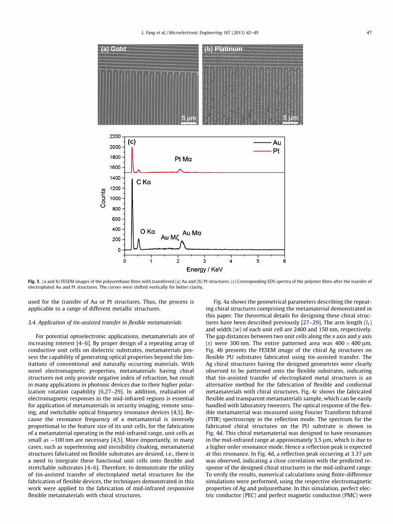
A significant advantage of electroplating is that it can easily de-posit different kinds of metal materials. This is one reason why theprocess is widely used in industry. Here, to demonstrate the utilityof tin-assisted-transfer in patterning different electroplated metalson flexible substrates, Au and Pt were electroplated on Au tem-plates and then transferred to PU substrates with the use of atin-assisted release layer. Fig. 3a and b presents the FESEM imagesof the flexible substrates after the transfer of Au and Pt structureswith a linewidth of 300 nm, respectively. Au structures (Fig. 3a)and Pt structures (Fig. 3b) were clearly found on the polymer sub-strates, indicating good transfer of Au and Pt to flexible substrateswith the help of the tin releasing layer. Fig. 3c shows the EDS dia-grams of the polymer substrates after the transfer of Au and Pt,respectively. Both Au and Pt peaks were observed on the polymersubstrates confirming that the tin-assisted transfer can also be
Fig. 3. (a and b) FESEM images of the polyurethane films with transferred (a) Au and (b) Pt structures. (c) Corresponding EDS spectra of the polymer films after the transfer ofelectroplated Au and Pt structures. The curves were shifted vertically for better clarity.
L. Fang et al. / Microelectronic Engineering 107 (2013) 42–49 47
used for the transfer of Au or Pt structures. Thus, the process isapplicable to a range of different metallic structures.
3.4. Application of tin-assisted transfer in flexible metamaterials
For potential optoelectronic applications, metamaterials are ofincreasing interest [4–6]. By proper design of a repeating array ofconductive unit cells on dielectric substrates, metamaterials pos-sess the capability of generating optical properties beyond the lim-itations of conventional and naturally occurring materials. Withnovel electromagnetic properties, metamaterials having chiralstructures not only provide negative index of refraction, but resultin many applications in photonic devices due to their higher polar-ization rotation capability [6,27–29]. In addition, realization ofelectromagnetic responses in the mid-infrared regions is essentialfor application of metamaterials in security imaging, remote sens-ing, and switchable optical frequency resonance devices [4,5]. Be-cause the resonance frequency of a metamaterial is inverselyproportional to the feature size of its unit cells, for the fabricationof a metamaterial operating in the mid-infrared range, unit cells assmall as �100 nm are necessary [4,5]. More importantly, in manycases, such as superlensing and invisibility cloaking, metamaterialstructures fabricated on flexible substrates are desired, i.e., there isa need to integrate these functional unit cells onto flexible andstretchable substrates [4–6]. Therefore, to demonstrate the utilityof tin-assisted transfer of electroplated metal structures for thefabrication of flexible devices, the techniques demonstrated in thiswork were applied to the fabrication of mid-infrared responsiveflexible metamaterials with chiral structures.
Fig. 4a shows the geometrical parameters describing the repeat-ing chiral structures comprising the metamaterial demonstrated inthis paper. The theoretical details for designing these chiral struc-tures have been described previously [27–29]. The arm length (l1)and width (w) of each unit cell are 2400 and 150 nm, respectively.The gap distances between two unit cells along the x axis and y axis(s) were 300 nm. The entire patterned area was 400 � 400 lm.Fig. 4b presents the FESEM image of the chiral Ag structures onflexible PU substrates fabricated using tin-assisted transfer. TheAg chiral structures having the designed geometries were clearlyobserved to be patterned onto the flexible substrates, indicatingthat tin-assisted transfer of electroplated metal structures is analternative method for the fabrication of flexible and conformalmetamaterials with chiral structures. Fig. 4c shows the fabricatedflexible and transparent metamaterials sample, which can be easilyhandled with laboratory tweezers. The optical response of the flex-ible metamaterial was measured using Fourier Transform Infrared(FTIR) spectroscopy in the reflection mode. The spectrum for thefabricated chiral structures on the PU substrate is shown inFig. 4d. This chiral metamaterial was designed to have resonancesin the mid-infrared range at approximately 3.5 lm, which is due toa higher order resonance mode. Hence a reflection peak is expectedat this resonance. In Fig. 4d, a reflection peak occurring at 3.37 lmwas observed, indicating a close correlation with the predicted re-sponse of the designed chiral structures in the mid-infrared range.To verify the results, numerical calculations using finite-differencesimulations were performed, using the respective electromagneticproperties of Ag and polyurethane. In this simulation, perfect elec-tric conductor (PEC) and perfect magnetic conduction (PMC) were
Fig. 4. (a) A schematic diagram of the chiral structures with l1 = 2.41 lm, l2 = 0.65 lm, w = 150 nm, s = 300 nm, and h = 78�. (b) A typical FESEM image of the Ag chiralstructures transferred onto a polyurethane film. (c) A photograph of the fabricated metamaterial printed film demonstrates its transparency and flexibility. (d) Reflectionspectra measured for the chiral metamaterial film is compared with simulation results determined for it.
48 L. Fang et al. / Microelectronic Engineering 107 (2013) 42–49
placed along the directions transverse to the direction of propaga-tion (Fig. 4a), forming the appropriate periodic boundary condi-tions. A detailed description of the simulation methods is givenin the experimental section. As shown in Fig. 4d, the simulationcurves matched well with the experimental results.
4. Conclusions
In summary, an alternative indirect patterning method, tin-as-sisted transfer of electroplated metal structures, was introducedfor the fabrication of flexible functional devices. That is, a releasinglayer of tin was introduced to facilitate the transfer of electroplatedmetal structures onto flexible substrates. Using tin-assisted trans-fer, electroplated sub-micron Ag, Au and Pt structures were suc-cessfully transferred to flexible substrates. This technique wasalso successfully employed for the fabrication of a flexible mid-infrared metamaterial comprised of repeating chiral structures,demonstrating the wide applicability of this process.
This method has several advantages. (1) Electroplating is aninexpensive and simple deposition method, enabling uniform largearea deposition. Using tin-assisted transfer, electroplated metalstructures were demonstrated for the fabrication of flexible andconformal devices. (2) The entire array of deposition and transferprocesses can be performed without requiring high vacuum, highpressure, or high temperature. (3) This technique can be poten-tially coupled with other lithography techniques, includingnanoimprinting or polymer pen lithography, for the fabrication oflarge area flexible devices. In addition to solution casting, othertransfer methods, such as roll-to-roll transfer, compression mold-ing, and thermoforming, can be used for high-rate fabrication.
Therefore, tin-assisted transfer of electroplated metal structuresis an attractive approach for the fabrication of flexible and confor-mal devices.
Acknowledgements
This research was funded by the Nanoscale Science and Engi-neering Centers program of the National Science Foundation(Award # NSF-0832785). We also appreciate the Kostas Centerfor the preparation of templates and Bruker Co. for thecharacterization.
References
[1] I. Park, S.H. Ko, H. Pan, C.P. Grigoropoulos, A.P. Pisano, J.M. Fréchet, E.S. Lee, J.H.Jeong, Adv. Mater. 20 (2008) 489.
[2] J. Lee, D.K. Hwang, J.M. Choi, K. Lee, J.H. Kim, S. Im, J.H. Park, E. Kim, Appl. Phys.Lett. 87 (2005) 023504.
[3] C.M. Hsu, C.L. Tsai, W.T. Wu, Appl. Phys. Lett. 88 (2006) 083515.[4] X. Xu, B. Peng, D. Li, J. Zhang, L.M. Wong, Q. Zhang, S. Wang, Q. Xiong, Nano
Lett. 11 (2011) 3232.[5] M. Walther, A. Ortner, H. Meier, U. Löffelmann, P.J. Smith, J.G. Korvink, Appl.
Phys. Lett. 95 (2009) 251107.[6] N. Wongkasem, A. Akyurtlu, K.A. Marx, W.D. Goodhue, L. Jin, Q. Dong, E.T. Ada,
Microsc. Res. Tech. 70 (2007) 497.[7] S.Y. Hwang, H.Y. Jung, J.H. Jeong, H. Lee, Thin Solid Films 517 (2009) 4104.[8] M.G. Kang, L.J. Guo, J. Vac. Sci. Technol. B 25 (2007) 2637.[9] Z. Wang, J. Yuan, J. Zhang, R. Xing, D. Yan, Y. Han, Adv. Mater. 15 (2003) 1009.
[10] D. Chanda, K. Shigeta, S. Gupta, T. Cain, A. Carlson, A. Mihi, A.J. Baca, G.R.Bogart, P. Braun, J.A. Rogers, Nat. Nanotechnol. 6 (2011) 402.
[11] J.W. Kim, K.Y. Yang, S.H. Hong, H. Lee, Appl. Surf. Sci. 254 (2008) 5607.[12] C.H. Chen, T.H. Yu, Y.C. Chen, J. Micromech. Microeng. 20 (2010) 025034.[13] H. Schmid, H. Wolf, R. Allenspach, H. Riel, S. Karg, B. Michel, E. Delamarche,
Adv. Funct. Mater. 13 (2003) 145.[14] L. Xu, S. Zhang, W. Liu, Z. Du, J. Phys. Chem. C 116 (2012) 2801.[15] J. Li, S. Ru, X. Fan, L. Huang, S. Sun, Langmuir 23 (2007) 13174.
L. Fang et al. / Microelectronic Engineering 107 (2013) 42–49 49
[16] G. Zhao, Y. He, Surf. Coat. Technol. 206 (2012) 4411.[17] M.J. Burek, A.S. Budiman, Z. Jahed, N. Tamura, M. Kunz, S. Jin, S.M.J. Han, G. Lee,
C. Zamecnik, T.Y. Tsui, Mater. Sci. Eng. A 528 (2011) 5822.[18] K.S. Salaita, S.W. Lee, D.S. Ginger, C.A. Mirkin, Nano Lett. 6 (2006) 2493.[19] T. Djenizian, P. Schmuki, J. Electroceram. 16 (2006) 9.[20] S. Gorelick, J. Vila-Comamala, V.A. Guzenko, C. David, Microelectron. Eng. 88
(2011) 2259.[21] F. Gao, S. Mukherjee, Q. Cui, Z. Gu, J. Phys. Chem. 113 (2009) 9546.[22] M. Wei, L. Fang, J. Lee, S. Somu, X. Xiong, C. Barry, A. Busnaina, J. Mead, Adv.
Mater. 21 (2009) 794.
[23] M. Wei, Z. Tao, X. Xiong, M. Kim, J. Lee, S. Somu, S. Sengupta, A. Busnaina, C.Barry, J. Mead, Macromol. Rapid Commun. 27 (2006) 1826.
[24] D. Kim, J. Kim, G.L. Wang, C.C. Lee, Mater. Sci. Eng. A 393 (2005) 315.[25] J. Doesburg, D.G. Ivey, Mater. Sci. Eng. B 78 (2000) 44.[26] J. Morales, L. Sánchez, F. Martín, J.R. Ramos-Barrado, M. Sánchez, J.
Electrochem. Soc. 151 (2004) A151.[27] N. Wongkasem, C. Kamtongdee, A. Akyurtlu, K.A. Marx, J. Opt. 12 (2010)
075102.[28] N. Wongkasem, A. Akyurtlu, J. Opt. 12 (2010) 035101.[29] K. Matra, N. Wongkasem, J. Opt. A-Pure Appl. Opt. 11 (2009) 074011.