29
•
Loughborough UniversityInstitutional Repository
Tin whisker mitigation bymeans of a
post-electroplatingelectrochemical oxidation
treatment
This item was submitted to Loughborough University's Institutional Repositoryby the/an author.
Citation: HASPEL, D. ...et al., 2015. Tin whisker mitigation by means ofa post-electroplating electrochemical oxidation treatment. Transactions of theInstitute of Metal Finishing , 93(6), pp.332-341.
Additional Information:
• This is an Accepted Manuscript of an article pub-lished by Taylor & Francis in Transactions of the Insti-tute of Metal Finishing on 11 Jan 2016, available online:http://www.tandfonline.com/10.1080/00202967.2015.1117258.
Metadata Record: https://dspace.lboro.ac.uk/2134/19834
Version: Accepted for publication
Publisher: c©Maney Publishing. Published on behalf of the Institute of MetalFinishing (IMF)
Rights: This work is made available according to the conditions of the Cre-ative Commons Attribution-NonCommercial-NoDerivatives 4.0 International(CC BY-NC-ND 4.0) licence. Full details of this licence are available at:https://creativecommons.org/licenses/by-nc-nd/4.0/
Please cite the published version.
Tin whisker mitigation by means of a post-electroplating
electrochemical oxidation treatment
D.M. Haspel1,3, M.A. Ashworth1, L. Wu1, G.D. Wilcox1 and R.J. Mortimer2
1.–Department of Materials, Loughborough University, Loughborough, Leicestershire, LE11 3TU, UK.
2.–Department of Chemistry, Loughborough University, Loughborough, Leicestershire, LE11 3TU, UK.
3.–e-mail: [email protected]
Abstract
There are very few studies that have investigated directly the effect of an oxide film on tin
whisker growth, since the ‘cracked oxide theory’ was proposed by Tu in 19941. The current
study has investigated the effect of an electrochemically produced oxide on tin whisker
growth, for both Sn-Cu electrodeposits on Cu and pure Sn electrodeposits on brass. X-ray
photoelectron spectroscopy (XPS) has been used to investigate the effect of the applied
electrochemical oxidation potential on the oxide film thickness. Focused ion beam (FIB) has
been used to prepare cross sections from electrodeposited samples to investigate the
influence of the electrochemically formed oxide film on deposit microstructure during long-
term room temperature storage. The XPS studies show that the thickness of
electrochemically formed oxide film is directly influenced by the applied potential and the
total charge passed. Whisker growth studies show that the electrochemical oxidation
treatment mitigates whisker growth for both Sn-Cu electrodeposits on Cu and pure Sn
electrodeposits on brass. For Sn electrodeposits on brass, the electrochemically formed
oxide greatly reduces both the formation of zinc oxide at the surface and the formation of
intermetallic compounds, which results in the mitigation of tin whisker growth. For Sn-Cu
electrodeposits on Cu, the electrochemically formed oxide has no apparent effect on
intermetallic compound formation and acts simply as a physical barrier to hinder tin whisker
growth.
Key words: Tin, electrochemical oxidation, electrodeposition, whisker growth, intermetallic
compounds
1 Introduction
A tin whisker is a growth of pure tin that is commonly in the form of a filament, which can
grow up to a few millimetres in length, from a thin tin coating (around 0.5-50 µm thick) that
has been electroplated onto a substrate2. The incubation period prior to the growth of a
whisker is uncertain and it is this unpredictability that causes concern to the reliable
operation of electronic components3. At the current time, there is no one widely accepted
mechanism for why and how whiskers grow; though there are number of theories and some
commonly agreed factors that affect the growth of tin whiskers2,4,5.
Whisker growth has been shown to cause major reliability problems in high value, long term
electronics, such as satellites and rocket systems, mainly due to these whiskers growing
from one surface and then coming into contact with another, adjacent surface, resulting in a
short circuit and subsequent electronic failure. Circuits can also short by long filament type
whiskers breaking off and landing across adjacent terminals. Both of these types of failures
occur at low currents. At high currents the whiskers can volatilise, which causes a
conductive metal gas, which in turn can create a metal vapour arc reaction6. This metal
vapour arc can generate such high temperatures that it can melt metals and incinerate
polymers.
Until recently, whisker growth was successfully mitigated by alloying tin with lead7,8.
However, restrictions on the use of lead, as result of EU legislation (RoHS), have led to a
renewed interest in finding alternative mitigation strategies. There are a number of
different mitigation techniques that are currently used to combat this problem, including
post-electroplating annealing, alloying, applying a polymeric conformal coating to act as a
physical barrier and the use of a nickel underlay to prevent intermetallic formation.9
There has been very little research on the role of the oxide layer in whisker growth. The
cracked oxide theory proposed by Tu1,10,11 suggested that the tin oxide film played a critical
role in the growth of tin whiskers and that a very thick oxide would physically block the
growth of filament whiskers or hillocks by reducing the risk of localised oxide cracking. For
whiskers to grow, it is first necessary to break the oxide film at weak points and from these,
the whiskers will subsequently grow to relieve stress12,13. It was suggested by Chang and
Vook14 that no whiskers will grow in the absence of an oxide film as the deposit would be
able to relieve internal stress by uniform creep of tin atoms to the deposit surface. However,
Moon et al15 later showed that whisker growth occurred on Sn-Cu electrodeposits that had
been stored for 9 days under vacuum with the surface oxide initially removed by ion beam
sputtering. A recent study carried out by Su et al16 showed the importance of weak points
in the oxide, by using 200 nm thick sputter deposited tin oxide films with pre-defined arrays
of weak spots built into the oxide film using lithography. It was observed that an increased
number of whiskers grew from samples that had a greater number of weak spots.
in a previous study17 the authors presented some initial results, which indicated that
whisker growth could be reduced by the application of an electrochemical oxide film. The
current paper builds upon this initial work to more fully investigate the influence of applied
potential and charge passed on the oxide film developed and its effect on whisker growth.
The effect of the electrochemical oxide treatment on the development of the deposit
microstructure during long-term storage is also investigated to more fully understand the
mechanism by which whisker growth is mitigated.
2 Experimental
2.1 Electrodeposition of Tin
Pure Sn was electrodeposited onto both Cu (Advent Research Materials, 99.9%, 0.1 mm and
0.4 mm thickness) and brass (Goodfellow, 63% Cu/37% Zn, 0.38 mm thickness) substrates,
using a bright acid Sn electroplating solution. A Sn-Cu alloy was also electroplated onto Cu
for whisker growth trials. The electroplating solution contained 60 g L-1 tin sulphate (Sigma
Aldrich), 70 ml L-1 sulphuric acid (Fisher Scientific) and 40 ml L-1 Tinmac Stannolyte
(MacDermid), a propriety additive that acts as a brightener. Electrodeposition of 2 µm and 5
μm pure Sn onto Cu and brass was carried out using a current density of 20 mA cm-2. For the
electrodeposition of Sn-Cu alloys the Sn electroplating bath was modified by the addition of
Cu ions at a concentration of 10 mmol L-1, using Cu sulphate. Electrodeposition of 2 μm Sn-
Cu onto Cu was carried out using a current density of 10 mA cm-2, which resulted in a
uniform electrodeposit with a Cu content of ~1 wt%.
The test coupons used had dimensions of 2 x 4 cm and were masked with chemically
resistant tape to result in an electroplated area of 2 x 2 cm. Larger test coupons with
dimensions 4 x 6 cm and an electroplated area of 4 x 4.5 cm were used for whisker growth
studies. The coupons were used in the as-supplied condition with no additional polishing or
grinding. Electrodeposition of pure Sn was carried out using a 99.95% Sn foil anode (Advent
Research Materials, 0.25 mm), whilst electrodeposition of the Sn-Cu was carried out using a
platinised titanium mesh anode. Immediately prior to electrodeposition, all the coupons
were degreased using acetone (Fisher Scientific), pickled for 60 s in a 20% v/v solution of
sulphuric acid (SG 1.83, Fisher Scientific), rinsed in deionised water and dried using hot air.
The thickness of pure Sn electrodeposits was 5 µm for cyclic voltammetry and
electrochemical oxidation trials. The thickness of pure Sn and Sn-Cu electrodeposits was 2
μm for whisker growth studies.
2.2 Preparation of the Electrolyte Solution for Tin Oxidation
For the electrochemical oxidation of the Sn electrodeposits two solutions were selected, a
pH 8.9 potassium bicarbonate-potassium carbonate solution (0.75 mol L-1 of potassium
bicarbonate, Sigma Aldrich, and 0.05 mol L-1 of potassium carbonate, Sigma Aldrich) and a
pH 8.4 borate buffer solution (9.55 g L-1 sodium borate, Sigma Aldrich, and 6.18 g L-1 boric
acid, Sigma Aldrich). Both electrolyte solutions were prepared using deionised water and
the pH was adjusted to the required value, using additions of sodium hydroxide (Fisher
Scientific).
2.3 Cyclic Voltammetry
Cyclic voltammetry was carried out for Sn electrodeposits in naturally aerated pH 8.9
potassium bicarbonate-potassium carbonate solution to determine the location of the
oxidation peaks. Analysis was carried out using a Solartron SI 1286 Electrochemical Interface
potentiostat by means of a 3-electrode cell comprising of a static Sn electrodeposit as the
working electrode, a saturated calomel reference electrode (SCE) and a platinised titanium
mesh counter electrode. The electrode potential was swept from a starting potential of -1.1
V down to -1.5 V, reversed up to 1.5 V and finally returned to -1.1 V (all versus SCE) using a
linear scan rate of 10 mV s-1.
2.4 Electrochemical Oxidation of Tin
Electrochemical oxidation was carried out immediately after tin electrodeposition using a
Solartron SI 1286 Electrochemical Interface potentiostat using the 3-electrode cell
previously described. Following immersion of the coupon into the naturally aerated
electrolyte solution, the Sn electrodeposit was initially held at a potential of -1.5 V vs. SCE to
reduce the pre-existing oxide. When hydrogen evolution was observed the surface was
agitated using a pipette to remove the bubbles and the potential was increased to the
desired value for oxidation.
2.5 Characterisation of Electrochemically Formed Oxides
Two charges were set as limits, 30 mC cm-2 and 60 mC cm-2. The effect of charge passed and
oxidation potential on the composition and thickness of the oxide film was investigated by
x-ray photoelectron spectroscopy (XPS) using a Thermo-Scientific K-Alpha x-ray
photoelectron spectrometer. Sputter depth profiling was carried out using 200 eV argon
ions with an estimated etch rate of ~0.01 nm s-1. XPS analysis was carried out within 24
hours of electrodeposition and electrochemical oxidation, unless otherwise stated.
2.6 Characterisation of Tin Deposits
The effect of an electrochemical oxide film on the microstructural evolution of
electrodeposited Sn and Sn-Cu alloys was investigated by means of cross-sections that were
prepared by focussed ion beam (FIB) milling, using a FEI Nova 600 Nanolab Dual Beam FIB-
SEM. Ion beam milling was carried out at a 52° tilt angle with 30 kV gallium ion beam. Initial
trench milling was carried out at 20 nA and the final face milling was carried out at 3 nA with
a tilt angle of 53.5°. Ion beam images were acquired using the gallium ion beam at a current
of 30 pA.
2.7 Whisker Growth Studies
The effect of the electrochemically formed oxides on whisker growth was assessed using 2
μm Sn electrodeposits on brass and 2 μm Sn-Cu electrodeposits on Cu. For each
electrochemical oxidation treatment three identical samples were prepared. After
electrodeposition and electrochemical oxidation, the samples were stored at room
temperature (~20 °C). The growth of whiskers was studied using both optical microscopy
and scanning electron microscopy (SEM). The density of whiskers was measured using an
optical microscope with an objective magnification of either x20 or x10. SEM analysis was
carried out using a Carl Zeiss Leo 1530 VP field emission gun SEM (FEGSEM) and an
operating voltage of 10 kV.
3 Results and Discussion
3.1 Development of the Electrochemical Oxide
Cyclic voltammetry was conducted using a standard potassium bicarbonate-carbonate
electrolyte to identify suitable potentials for subsequent electrochemical oxidation trials
(figure [1]). Two oxidations peaks (I and II) were recorded at potentials of -0.83 V and -0.66
V vs. SCE respectively. Peaks I and II have been attributed previously to the two Sn oxidation
states, Sn(II) and Sn(IV) respectively18,19. However, Díaz et al20 have also suggested that
oxidation peaks I and II both corresponded to the oxidation of Sn to Sn(II).
The potentials chosen for electrochemical oxidation studies, were -0.66 V (II), -0.5 V (III), -
0.4 V (IV), 0 V (V) and 1.2 V (VI) (all vs. SCE). Oxidation peak I (-0.83 V vs. SCE) was not
studied because it had previously been shown to produce an oxide film comparable to a
native oxide17. The electrochemical oxidation potentials -0.4 V and -0.5 V vs. SCE were
chosen as they occurred upon the broad trailing slope of the second oxidation peak which
would suggest large amounts of activity within this region and it was suggested by
Drogowska et al19 that this broad slope corresponds to a dehydration reaction that results in
the formation of SnO2. The electrochemical oxidation potential of 0 V vs. SCE was chosen as
it occurred on the part of the voltammogram that had the lowest anodic current, which was
suggested by Drogowska et al19 to be the region of passivity. The electrochemical oxidation
potential of 1.2 V vs. SCE was chosen as it was previously shown to produce a thick oxide
film17.
The effect of electrochemical oxidation potential on the Sn oxide thickness, for a charge
passed of 30 mC cm-2, is shown in the XPS high resolution scans of the Sn 3d peak in figure
[2]; a high resolution Sn 3d scan of a native air-formed oxide is also shown for comparison.
The relative intensity of the Sn oxide and Sn metal peaks, at ~487 eV and ~485 eV
respectively, enables the comparative thickness of the oxide layer to be inferred. It is
evident from figure [2] that the native air-formed oxide is very thin compared with oxide
films that are formed electrochemically. Results show that the thickest electrochemical
oxide film was produced at a potential of 1.2 V vs. SCE, which is consistent with previous
trials17. The Sn oxide and Sn metal contributions as a function of electrochemical oxidation
potential are summarised in table [1], which clearly indicates that the thickness of the Sn
oxide increases as the oxidation potential is increased.
Samples with electrochemically formed oxides were analysed using SEM to study the effect
of electrochemical oxidation on the surface of the Sn electrodeposit. It is apparent from
figure [3] that electrochemical oxidation at certain potentials (e.g. -0.66 V vs. SCE) can have
a pronounced effect on the surface topography. However, the surface of samples
electrochemically oxidised at a potential of 1.2 V vs. SCE (30 mC cm-2 of charge passed) is
indistinguishable from that of a native air-formed oxide. Increasing the amount of charge
passed, increases the extent of the surface roughening for samples electrochemically
oxidised at a potential of -0.66 V vs. SCE (figure [3c]). This may suggest that a Sn dissolution
reaction has occurred. The size and shape of the surface features are comparable to that of
the Sn grains. Similar features were also observed in an earlier study by Ashworth et al17 for
electrochemical oxidation at same the potential.
Further electrochemical oxidation trials were undertaken using the potassium bicarbonate-
potassium carbonate solution, at potentials greater than 1.2 V vs. SCE, in an attempt to
increase the electrochemical oxide film thickness. The observed reduction in the intensity of
the Sn metal peak with increasing electrochemical oxidation potential (figure [4]) suggests
that the oxide film thickness is increased. This is consistent with previous trials by Ashworth
et al17 using the same potentials in a borate buffer solution. As the electrochemical
oxidation potential was increased from 1.2 V to 2.0 V vs. SCE the binding energy of the Sn
oxide peak shifted from 487 eV to 486.8 eV. However, this does not necessarily indicate a
difference in the oxide formed as the binding energies all fall within the binding energy
range for SnO221.
Depth profiling was carried out on each sample to confirm that electrochemical oxidation at
potentials above 1.2 V vs. SCE does increase the thickness of the oxide. The depth profiles in
figure [5] confirm that the oxide film increases in thickness with increasing electrochemical
oxidation potential. Results show that when electrochemical oxidation is carried out at a
potential of 2.0 V vs. SCE the thickness of the oxide film increases by ~75% compared with a
potential of 1.2 V vs. SCE. An increase in the thickness of the oxide film should have a
beneficial effect on whisker mitigation1,10,11.
The effect of electrochemical oxidation on whisker growth was studied using 2 μm Sn-Cu
electrodeposits on Cu and 2 μm Sn electrodeposits on brass. The Sn-Cu electrodeposits
were oxidised at potentials ranging between -0.66 V and 2.0 V vs. SCE in a potassium
bicarbonate-carbonate solution. The Sn electrodeposits on brass were oxidised at potentials
ranging between 1.2 V and 2.0 V vs. SCE. In each case, control samples were prepared and
left to develop native air-formed oxide films.
3.2 Whisker Growth Studies
3.2.1 Sn-Cu electrodeposits on Cu For whisker growth studies using Sn-Cu electrodeposits on Cu, electrochemical oxidation
was carried out at potentials of -0.66 V, -0.5 V, -0.4 V, 0.0 V and 1.2 V (all versus SCE). Large
test coupons were used, which contained three different areas of oxide; two areas were
electrochemically oxidised with a different charge passed applied in each area (achieved by
sequentially lowering the test coupon into the electrolyte; the other area was left to
develop a native air-formed oxide (figure [6]). Whiskers were counted on each area after ~2
months of storage and whisker densities were calculated (figure [7]). An important
observation is that there is a large difference in the whisker densities for the native oxides,
ranging from ~1200 cm-2 to ~3700 cm-2. There are a number of possible explanations for this
difference: firstly whisker growth is, by nature, unpredictable and sample to sample
variations in whisker density are not uncommon22. Secondly, there may be slight variations
in the Cu content of the deposit, due to either Sn or Cu depletion since an inert counter
electrode is being used and the electroplating bath is not being replenished with fresh metal
ions.
For a charge passed of 30 mC cm-2 electrochemical oxidation at 1.2 V, 0 V and -0.66 V vs. SCE
(figure [7]) resulted in a reduction in whisker growth. However, electrochemical oxidation at
potentials of -0.4 V and -0.5 V vs. SCE resulted in an increase in whisker density, despite the
fact that the oxide film is thicker than that of the native oxide. Further work is planned to
investigate the cause of the increased whisker growth.
For a charge passed of 60 mC cm-2, all of the electrochemical oxide films significantly
reduced the whisker density compared with the corresponding native oxide film (figure [7]).
This reduction in whisker density is mostly likely due to the presence of a thicker oxide film,
which would be in agreement with Tu’s cracked oxide theory1,10,11, which proposed that a
thicker oxide would reduce oxide cracking. The reduction in whisker density for samples
electrochemically oxidised at potentials of -0.4 V and -0.5 V vs. SCE suggests that a minimum
threshold charge has to be passed before a stable oxide is formed that can reduce whisker
growth.
Results show that the greatest whisker mitigation is obtained for samples electrochemically
oxidised at potentials of 1.2 V and -0.66 V vs. SCE, both these potentials reduced whisker
density at each of the charges passed producing a reduction of over 80% compared with the
corresponding native oxide
For electrochemical oxidation at potentials of 1.2 V, 1.6 V and 2.0 V (vs. SCE), samples with
an electroplated area of 2 x 2 cm were used. Table [2] shows that as the applied oxidation
potential is increased, from 1.2 V to 2.0 V vs. SCE, the whisker density is further reduced.
The reduction in whisker growth can be directly related to the Sn oxide depth profiles in
figure [5], which showed that oxidation at potentials greater than 1.2 V vs. SCE resulted in
an increase in oxide thickness. Table [2] also shows that the number of frames (out of 60)
where no whiskers were observed was considerably higher for the electrochemically
oxidised samples and increased slightly with increasing oxidation potential. The large
number of frames with no whiskers present results in a high standard deviation, relative to
the measured whisker density, for the electrochemically oxidised samples.
To more fully understand the mechanism by which whisker mitigation is accomplished for
the electrochemically oxidised samples, FIB analysis was carried on Sn-Cu electrodeposits on
Cu after storage at room temperature for ~24 months.
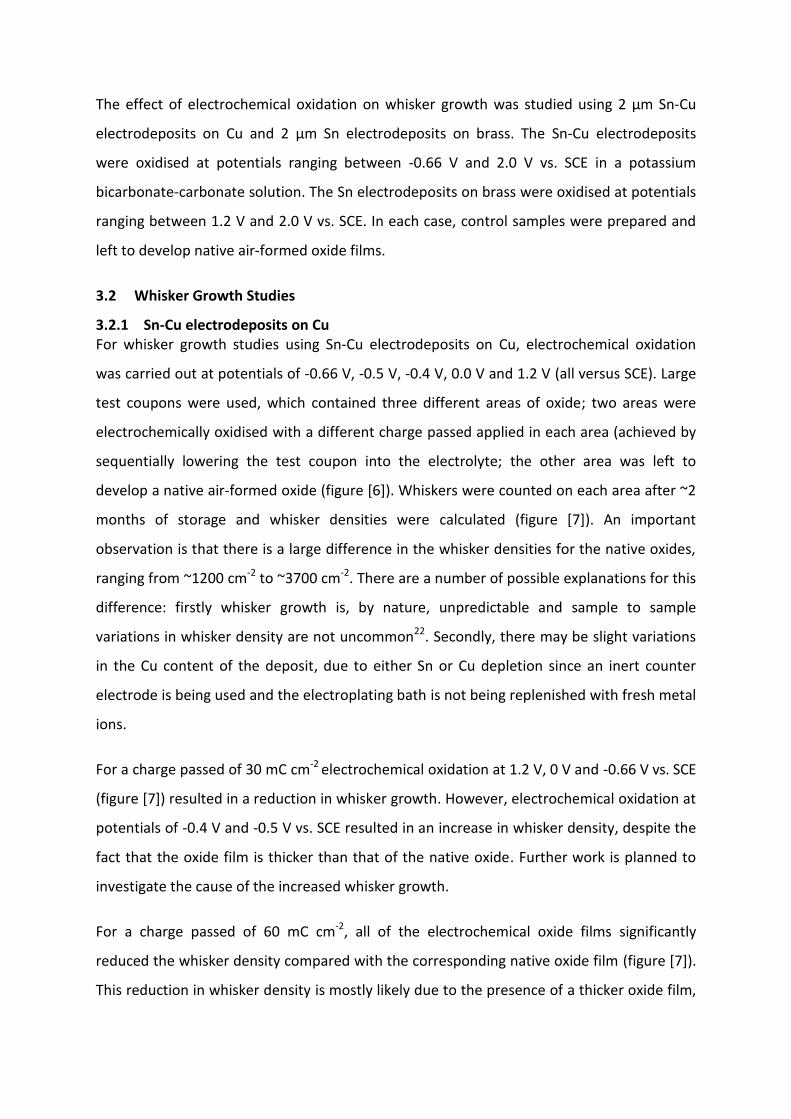
Figure [8] shows FIB cross-sections obtained from two Sn-Cu on Cu samples after storage at
room temperature for 24 months; the first left to develop a native oxide (figure [8a]) and
the second electrochemically oxidised at 1.2 V vs. SCE in potassium bicarbonate-carbonate
(figure [8b]). It can be seen that extensive intermetallic formation has occurred in both
samples, i.e. the presence of the electrochemical oxide has had no observable effect on
intermetallic growth, which is the primary driving force for whisker growth in these
samples8,23,24. This suggests that the reduced whisker growth observed for the
electrochemically oxidised samples results from the thicker electrochemical oxide providing
an enhanced physical barrier to the growth of whiskers rather than the driving force for
whisker growth being reduced. This observation supports Tu’s theory1,10,11, which proposed
that a thicker oxide will mitigate whisker growth by acting as a physical barrier and reduce
the risk of localised cracking.
XPS depth profiles obtained from the surface of these samples are shown in figure [9],
together with a one day old native oxide. After storage at room temperature for ~24 months
the Sn oxide thickness is greatly increased for the sample left to develop the native oxide
and is approaching the thickness of the electrochemically oxidised sample. The more
gradual reduction in oxygen content with depth for the sample with the native oxide after
~24 months storage (figure [9b]) indicates that significant inward diffusion of oxygen into
the electrodeposit has occurred. In comparison, the oxygen content drops off more rapidly
for the electrochemically oxidised sample. This suggests that the electrochemical oxide film
may act as a diffusion barrier to prevent the inward diffusion of oxygen into the
electrodeposit.
3.2.2 Sn electrodeposits on brass
For electrochemical oxidation at potentials of 1.2 V, 1.6 V and 2.0 V (vs. SCE), samples with
an electroplated area of 2 x 2 cm were used. Table [3] shows that for Sn electrodeposits on
brass, whisker growth is dramatically reduced by the electrochemical oxidation treatments.
Furthermore, as the applied oxidation potential is increased the whisker density is further
decreased. The slight reduction in whisker growth at the higher oxidation potentials can be
directly related to the relative intensities of the Sn3d5 oxide and Sn3d5 metals peaks shown
in previous work17 which indicated that oxidation at potentials greater than 1.2 V vs. SCE
resulted in an increase in oxide thickness.
To more fully understand the whisker mitigation mechanism, FIB analysis was carried on Sn
electrodeposits on brass after storage at room temperature for ~30 months.
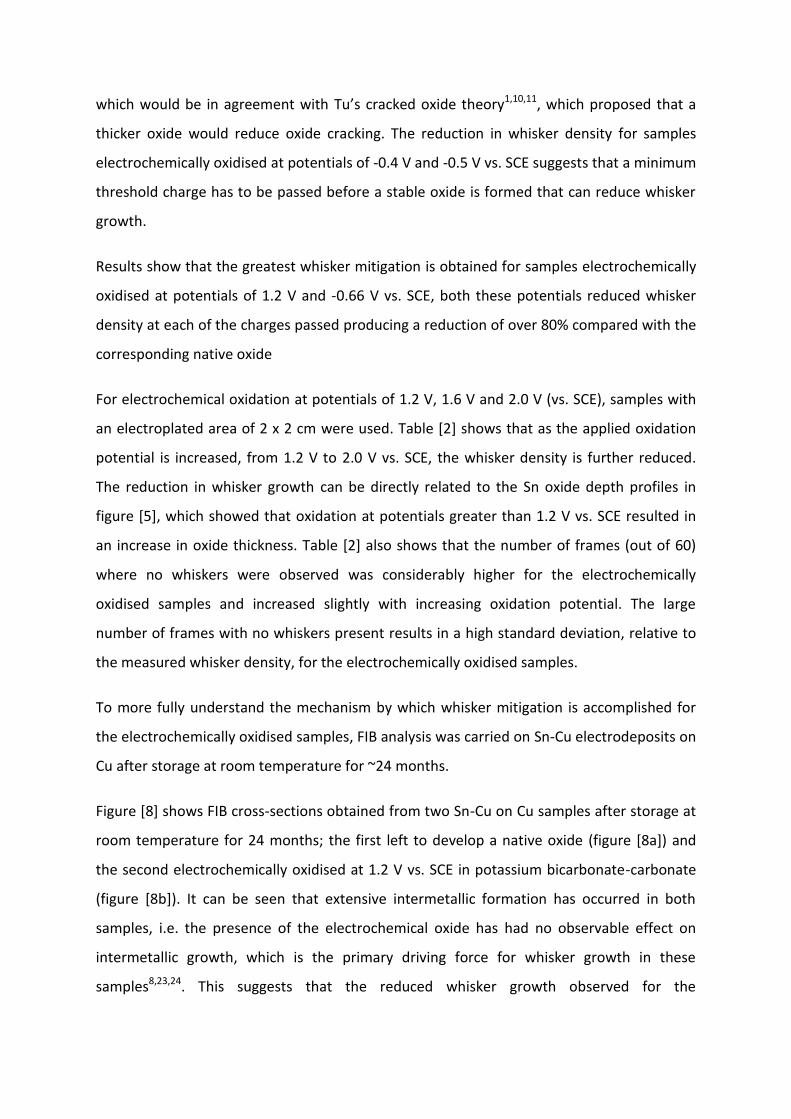
Figure [10] shows FIB cross-sections of two Sn on brass samples, with the first left to
develop a native oxide (figure [10a]) and the second with an electrochemical oxide formed
at 1.2 V vs. SCE in borate buffer (figure [10b]). Figure [10a] clearly shows both zinc oxide, at
the deposit surface, and Cu6Sn5 intermetallic formation at the Sn-brass interface, both of
which are known to cause whisker growth8,17,23–25, by generating internal stresses within the
electrodeposited coating. In comparison figure [10b] shows that no zinc oxide formation has
occurred at the surface of the electrochemically oxidised electrodeposit and only limited
intermetallic formation has occurred at the Sn-Cu interface after ~30 months of storage.
XPS depth profiles obtained from the same samples are shown in figure [11] together with a
depth profile, measured after ~24 hours, from a tin electrodeposit on brass left to develop a
native oxide (figure [11a]). Comparison of the samples left to develop native oxides after 1
day and 30 months shows that the amount of zinc and oxygen present at the deposit
surface greatly increases, which corresponds to the formation of zinc oxide at the surface.
By comparison, zinc diffusion to the surface of the electrochemically oxidised deposit is
prevented by the presence of the thicker Sn oxide film, which was produced shortly after
the deposition of the Sn17. Since high zinc concentrations are built up beneath the Sn oxide,
but FIB analyses suggest that no zinc oxide is present within the electrochemically oxidised
Sn, it may be inferred that the electrochemically formed Sn oxide is preventing the inward
diffusion of oxygen atoms into the electrodeposit.
These results demonstrate that the electrochemically formed oxide acts as a diffusion
barrier and prevents the formation of zinc oxide at the electrodeposit surface, which
prevents the development of internal stresses. The effect of the electrochemical oxidation
treatment on the development of the Cu6Sn5 intermetallic is, perhaps, more surprising,
since it was not expected that the electrochemically formed oxide would have an influence
on the Cu6Sn5 intermetallic growth.
4 Conclusions
The application of an electrochemical oxidation treatment has been demonstrated to
successfully mitigate whisker growth for both Sn-Cu deposits on Cu and pure Sn deposits on
brass.
For Sn-Cu deposits on Cu, the presence of the electrochemical oxide has no influence on the
principal driving force for whisker growth, i.e. intermetallic formation, and whisker
mitigation is derived from the thicker electrochemical oxide providing an enhanced physical
barrier. The presence of a thicker oxide layer mitigates whisker growth by reducing the risk
of localised cracking in the oxide film through which whiskers may subsequently grow.
For electrochemically oxidised pure Sn deposits on brass, whisker mitigation is achieved by
preventing the formation of zinc oxide at the deposit surface and also by greatly reducing
the growth of Cu6Sn5 intermetallic at the Sn-Cu interface, i.e. the driving forces for whisker
growth are diminished. The electrochemical oxide may also function as a physical barrier to
whisker growth in a manner analogous to that observed for the Sn-Cu deposits.
The thickness of the electrochemically formed oxide film is directly related to the applied
potential and the total amount of charge passed. For an equivalent charge passed, the
thickest oxide film, and most effective whisker mitigation, was obtained for samples
electrochemically oxidised at the highest potentials studied, i.e. 1.2-2.0 V vs. SCE.
5 Acknowledgements
The authors would like to both the UK EPSRC Innovative Electronics Manufacturing Research
Centre for funding this research through the WHISKERMIT programme and the
Loughborough University Materials Research School.
6 References
1. Tu K-N. Irreversible processes of spontaneous whisker growth in bimetallic Cu-Sn thin film reactions. Phys. Rev. 1994;49(3):2030–2034.
2. Galyon GT. Annotated Tin Whisker Bibliography and Anthology. Trans. on Elect. Pack. Manu. 2005;28(1):94–122.
3. Compton KG, Medizza A, Arnold SM. Filamentary growths on metal surfaces – whiskers. Corrosion. 1951;7(10):327–334.
4. Chason E, Jadhav N, Pei F, Buchovecky E, Bower A. Growth of whiskers from Sn surfaces: Driving forces and growth mechanisms. Progress in Surface Science. 2013;88(2):103–131.
5. Zhang P, Zhang YM, Sun ZM. Spontaneous Growth of Metal Whiskers on Surfaces of Solids: A Review. J. Mat. Sci. & Tech. 2015;31(7):675–698.
6. Han S, Osterman M, Pecht M. Likelihood of Metal Vapor Arc by Tin Whiskers. SMT Magazine. 2012 Aug:48–56.
7. Arnold SM. Repressing the Growth of Tin Whiskers. Plating. 1966;53(1):96–99.
8. Boettinger WJ, Johnson C, Bendersky L, Moon K, Williams M, Stafford G. Whisker and hillock formation on Sn, Sn-Cu and Sn-Pb electrodeposits’. Acta Materialia. 2005;53(19):5033–5050.
9. Osterman M. Mitigation strategies for tin whiskers. CALCE EPSC. 2002 [accessed 2015 Jun 8]. http://www.calce.umd.edu/tin-whiskers/TINWHISKERMITIGATION.pdf
10. Tu K-N, Zeng K. Reliability Issues of Pb-free Solder Joints in Electronic Packaging Technology. Proceedings of the IEEE Electronic Components and Technology Conference,. 2002:1194–1200.
11. Tu K-N, Chen C, Wu AT. Stress analysis of spontaneous Sn whisker growth. J. Mat. Sci. 2007;18(1-3):269–281.
12. Kumar KS, Reinbold L, Bower AF, Chason E. Plastic deformation processes in Cu/Sn bimetallic films. J. Mat. Res. 2008;23(11):2916–2934.
13. Lee BZ, Lee DN. Spontaneous growth mechanism of tin whiskers. Acta Materialia. 1998;46(10):3701–3714.
14. Chang CY, Vook RW. The effect of surface aluminum oxide films on thermally induced hillock formation. Thin Solid Films. 1993;228(1-2):205–209.
15. Moon K-W, Johnson CE, Williams ME, Kongstein O, Stafford GR, Handwerker CA, Boettinger WJ. Observed Correlation of Sn Oxide Film to Sn Whisker Growth in Sn-Cu Electrodeposit for Pb-Free Solders. J. Electron. Mat. 2005;34(9):L31–L33.
16. Su C-H, Chen H, Lee H-Y, Liu CY, Ku C-S, Wu AT. Kinetic Analysis of Spontaneous Whisker Growth on Pret-treated Surfaces with Weak Oxide. J. Electron. Mat. 2014;43(9):3290–3295.
17. Ashworth MA, Haspel D, Wu L, Wilcox GD, Mortimer RJ. An Investigation into the Effect of a Post-electroplating Electrochemical Oxidation Treatment on Tin Whisker Formation. J. Electron. Mat. 2015;44(1):442–456.
18. Alvarez P, Ribotta S, Folquer M. Potentiodynamic behaviour of tin in different buffer solutions. Corr. Sci. 2002;44(1):49–65.
19. Drogowska M, Ménard H, Brossard L. Electrochemical behaviour of tin in bicarbonate solution at pH 8. J. Appl. Electrochem. 1991;21(1):84–90.
20. Díaz R, Díez-Pérez I, Gorostiza P, Sanz F, Morante JR. An Electrochemical Study of Tin Oxide Thin Film in Borate Buffer Solutions. J. Braz. Chem. Soc. 2003;14(4):523–529.
21. NIST. X-ray Photoelectron Spectroscopy Database. NIST Stand. Ref. Database 20, Version 20. [accessed 2015 Sep 3]. http://srdata.nist.gov/xps/
22. Ashworth MA, Wilcox GD, Higginson RL, Heath RJ, Liu C, Mortimer RJ. The effect of electroplating parameters and substrate material on tin whisker formation. Microelectronics Reliability. 2015;55(1):180–191.
23. Tu K-N, Suh J, Wu AT-C, Tamura N, Tung C-H. Mechanism and Prevention of Spontaneous Tin Whisker Growth. Mat. Trans. 2005;46(11):2300–2308.
24. Chason E, Jadhav N, Chan WL, Reinbold L, Kumar KS. Whisker formation in Sn and Pb-Sn coatings; Role of intermetallic growth, stress evolution, and plastic deformation processes. Appl. Phys. Lett. 2008;92(17):171901–171901–3.
25. Ashworth MA, Wilcox GD, Higginson RL, Heath RJ, Liu C. An investigation into Zinc diffusion and tin whisker growth for electroplated tin deposits on brass. J. Electron. Mat. 2014;43(4):1005–1016.
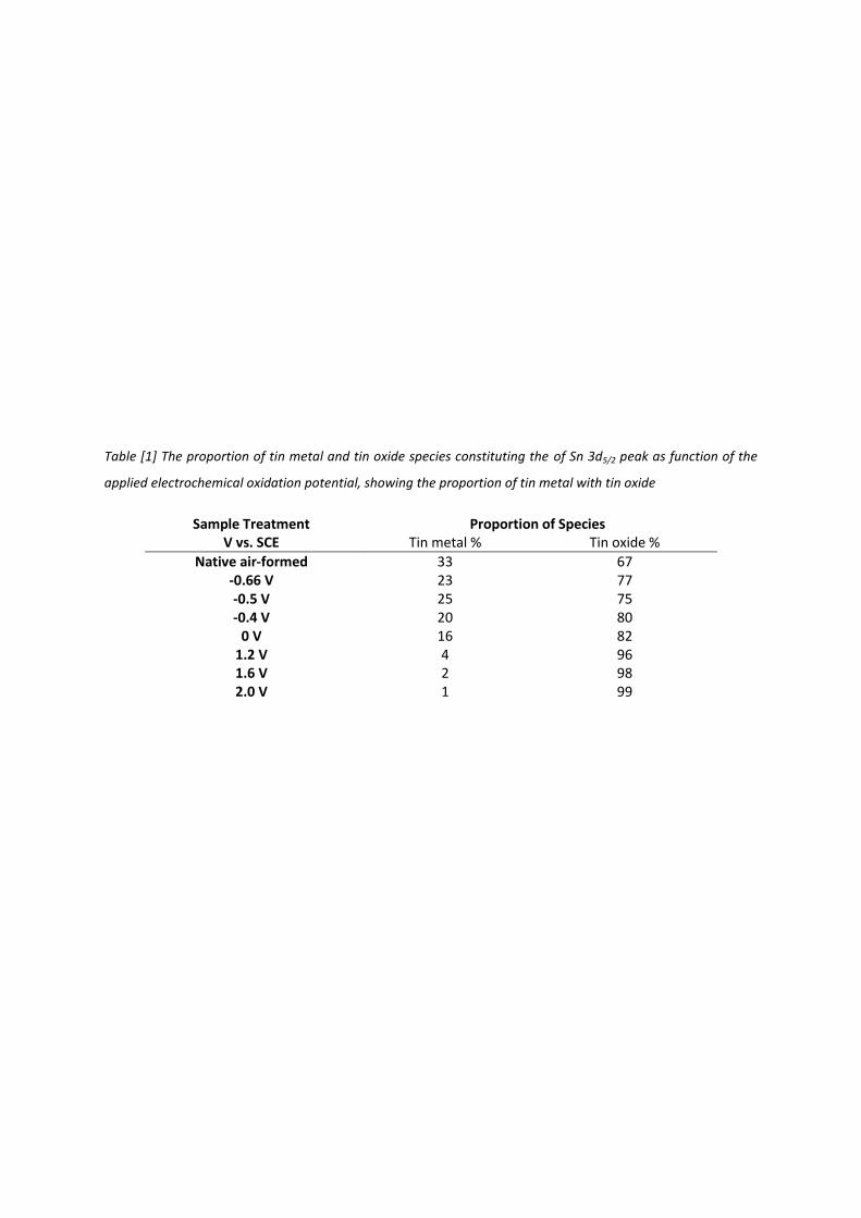
Table [1] The proportion of tin metal and tin oxide species constituting the of Sn 3d5/2 peak as function of the
applied electrochemical oxidation potential, showing the proportion of tin metal with tin oxide
Sample Treatment V vs. SCE
Proportion of Species Tin metal % Tin oxide %
Native air-formed 33 67
-0.66 V 23 77
-0.5 V 25 75
-0.4 V 20 80
0 V 16 82
1.2 V 4 96
1.6 V 2 98
2.0 V 1 99
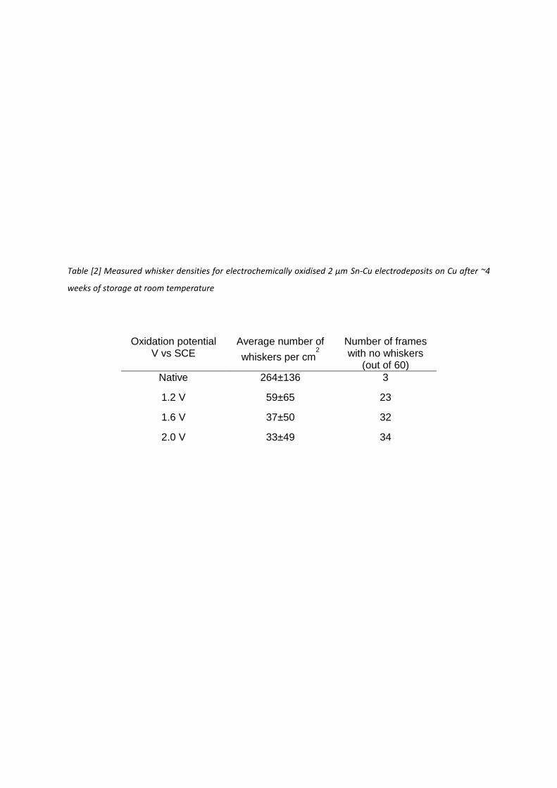
Table [2] Measured whisker densities for electrochemically oxidised 2 µm Sn-Cu electrodeposits on Cu after ~4
weeks of storage at room temperature
Oxidation potential V vs SCE
Average number of
whiskers per cm2
Number of frames with no whiskers
(out of 60)
Native 264±136 3
1.2 V 59±65 23
1.6 V 37±50 32
2.0 V 33±49 34
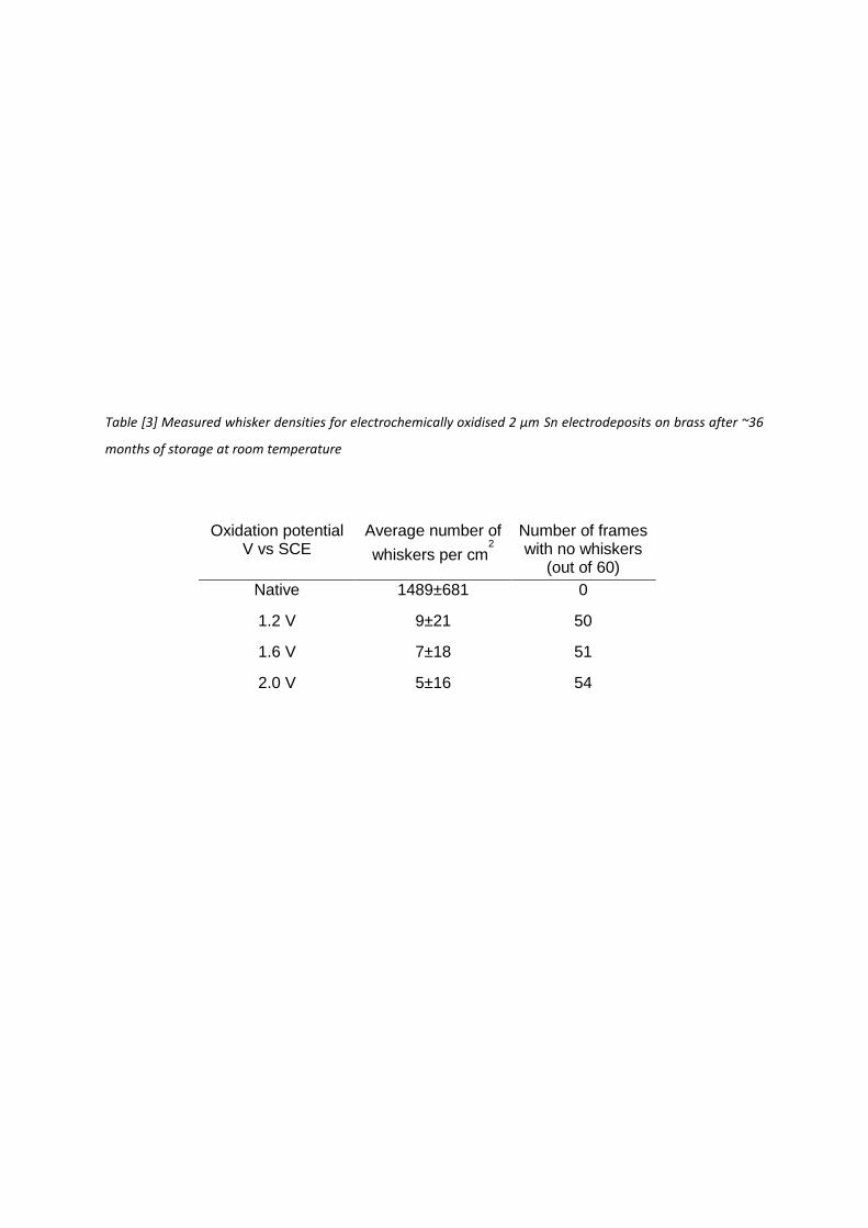
Table [3] Measured whisker densities for electrochemically oxidised 2 µm Sn electrodeposits on brass after ~36
months of storage at room temperature
Oxidation potential V vs SCE
Average number of
whiskers per cm2
Number of frames with no whiskers
(out of 60)
Native 1489±681 0
1.2 V 9±21 50
1.6 V 7±18 51
2.0 V 5±16 54
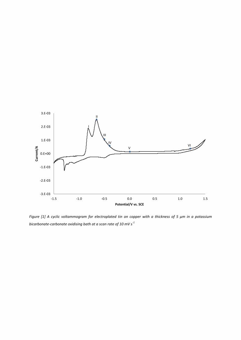
Figure [1] A cyclic voltammogram for electroplated tin on copper with a thickness of 5 µm in a potassium
bicarbonate-carbonate oxidising bath at a scan rate of 10 mV s-1
-3.E-03
-2.E-03
-1.E-03
0.E+00
1.E-03
2.E-03
3.E-03
-1.5 -1.0 -0.5 0.0 0.5 1.0 1.5
Cu
rre
nt/
A
Potential/V vs. SCE
I
II
III
IV
V VI
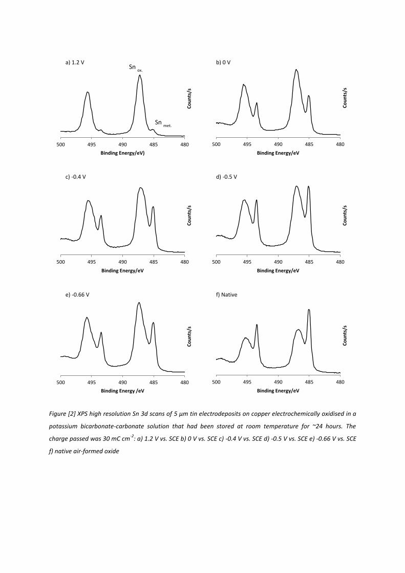
Figure [2] XPS high resolution Sn 3d scans of 5 µm tin electrodeposits on copper electrochemically oxidised in a
potassium bicarbonate-carbonate solution that had been stored at room temperature for ~24 hours. The
charge passed was 30 mC cm-2
: a) 1.2 V vs. SCE b) 0 V vs. SCE c) -0.4 V vs. SCE d) -0.5 V vs. SCE e) -0.66 V vs. SCE
f) native air-formed oxide
480485490495500
Co
un
ts/s
Binding Energy/eV
480485490495500
Co
un
ts/s
Binding Energy/eV)
480485490495500
Co
un
ts/s
Binding Energy/eV
480485490495500
Co
un
ts/s
Binding Energy/eV
480485490495500
Co
un
ts/s
Binding Energy/eV
480485490495500
Co
un
ts/s
Binding Energy /eV
a) 1.2 V b) 0 V
c) -0.4 V d) -0.5 V
e) -0.66 V f) Native
Sn ox.
Sn met.
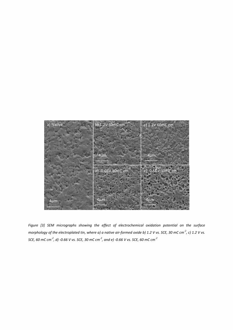
Figure [3] SEM micrographs showing the effect of electrochemical oxidation potential on the surface
morphology of the electroplated tin, where a) a native air-formed oxide b) 1.2 V vs. SCE, 30 mC cm-2
, c) 1.2 V vs.
SCE, 60 mC cm-2
, d) -0.66 V vs. SCE, 30 mC cm-2
, and e) -0.66 V vs. SCE, 60 mC cm-2
b) 1.2V 30mC cm-2
4µm
d) -0.66V 30mC cm-2
4µm
c) 1.2V 60mC cm-2
4µm
e) -0.66V 60mC cm-2
4µm 4µm
a) Native
Figure [4] XPS high resolution scans of the Sn 3d peaks after electrochemical oxidation in a potassium
bicarbonate-carbonate solution at potentials of 1.2 V (solid), 1.6 V (square dot) and 2.0 V (dash) all versus SCE
480485490495500
Co
un
ts/s
Binding Energy/eV
1.2V
1.6V
2.0V
small energy shift in the oxide peak
Reduction in metal peak with increasing potential
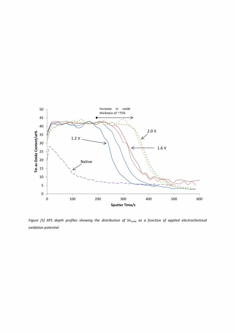
Figure [5] XPS depth profiles showing the distribution of Snoxide as a function of applied electrochemical
oxidation potential
0
5
10
15
20
25
30
35
40
45
50
0 100 200 300 400 500 600
Tin
as
Oxi
de
Co
nte
nt/
at%
Sputter Time/s
Increase in oxide thickness of ~75%
Native
2.0 V
1.6 V
1.2 V
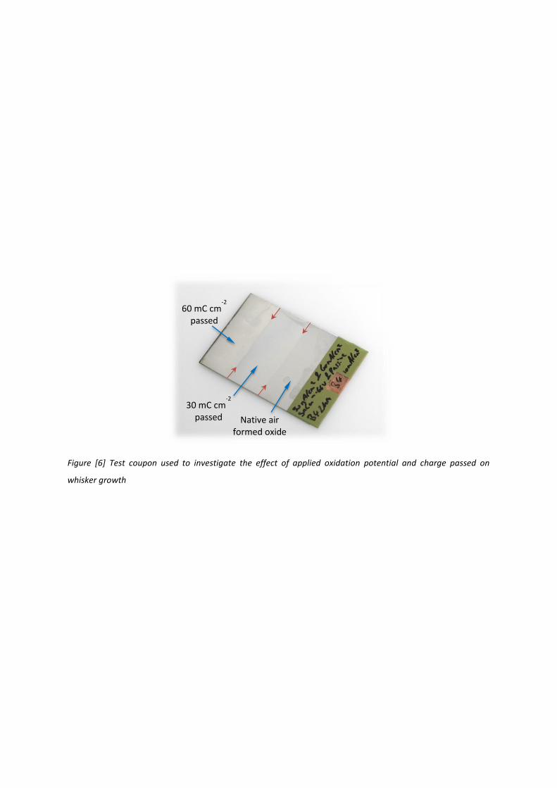
Figure [6] Test coupon used to investigate the effect of applied oxidation potential and charge passed on
whisker growth
Native air formed oxide
30 mC cm-2
passed
60 mC cm-2
passed
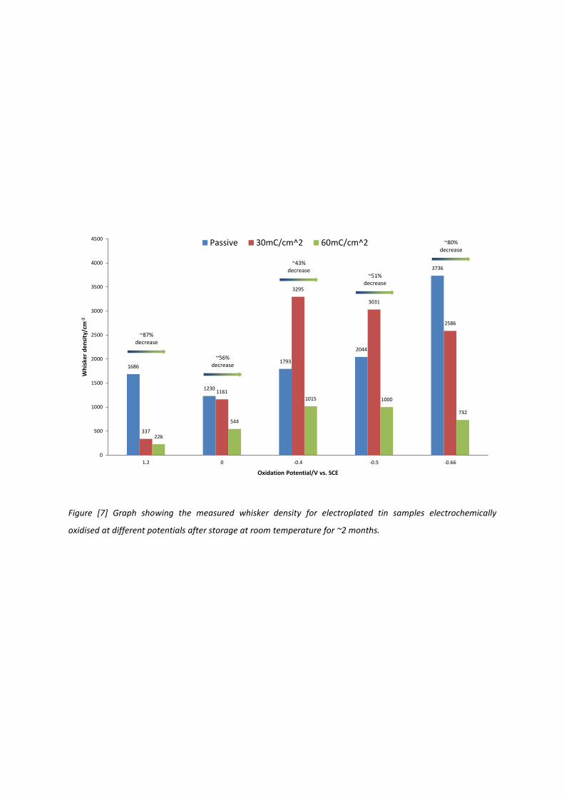
Figure [7] Graph showing the measured whisker density for electroplated tin samples electrochemically
oxidised at different potentials after storage at room temperature for ~2 months.
1686
1230
1793
2044
3736
337
1161
3295
3031
2586
226
544
1015 1000
732
0
500
1000
1500
2000
2500
3000
3500
4000
4500
1.2 0 -0.4 -0.5 -0.66
Wh
iske
r d
ensi
ty/c
m-2
Oxidation Potential/V vs. SCE
Passive 30mC/cm^2 60mC/cm^2
~43% decrease
~56% decrease
~87% decrease
~51% decrease
~80% decrease
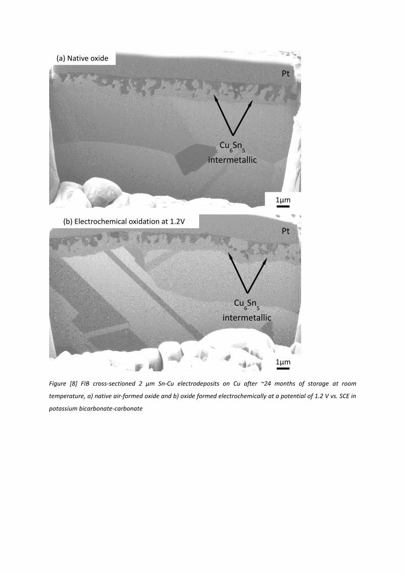
Figure [8] FIB cross-sectioned 2 µm Sn-Cu electrodeposits on Cu after ~24 months of storage at room
temperature, a) native air-formed oxide and b) oxide formed electrochemically at a potential of 1.2 V vs. SCE in
potassium bicarbonate-carbonate
1µm
1µm
(a) Native oxide
(b) Electrochemical oxidation at 1.2V
Cu6Sn
5
intermetallic
Cu6Sn
5
intermetallic
Pt
Pt
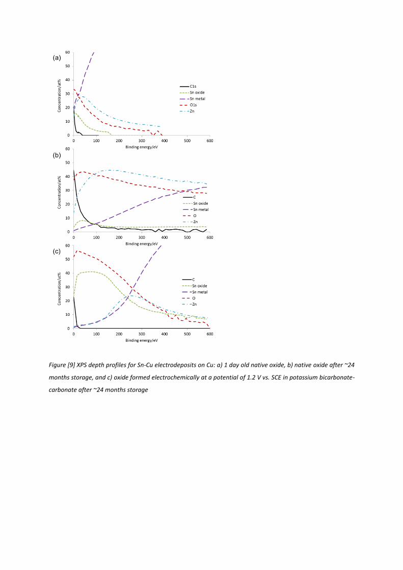
Figure [9] XPS depth profiles for Sn-Cu electrodeposits on Cu: a) 1 day old native oxide, b) native oxide after ~24
months storage, and c) oxide formed electrochemically at a potential of 1.2 V vs. SCE in potassium bicarbonate-
carbonate after ~24 months storage
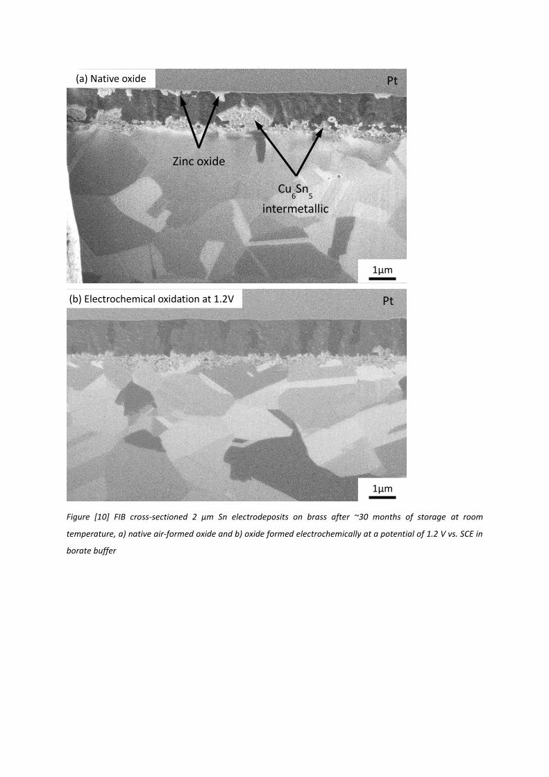
Figure [10] FIB cross-sectioned 2 µm Sn electrodeposits on brass after ~30 months of storage at room
temperature, a) native air-formed oxide and b) oxide formed electrochemically at a potential of 1.2 V vs. SCE in
borate buffer
1µm
1µm
(a) Native oxide
(b) Electrochemical oxidation at 1.2V
Zinc oxide
Cu6Sn
5
intermetallic
Pt
Pt
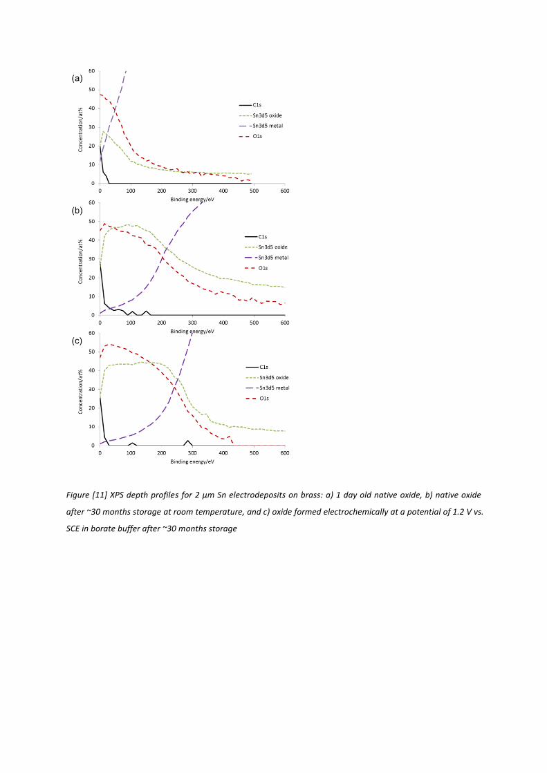
Figure [11] XPS depth profiles for 2 µm Sn electrodeposits on brass: a) 1 day old native oxide, b) native oxide
after ~30 months storage at room temperature, and c) oxide formed electrochemically at a potential of 1.2 V vs.
SCE in borate buffer after ~30 months storage


