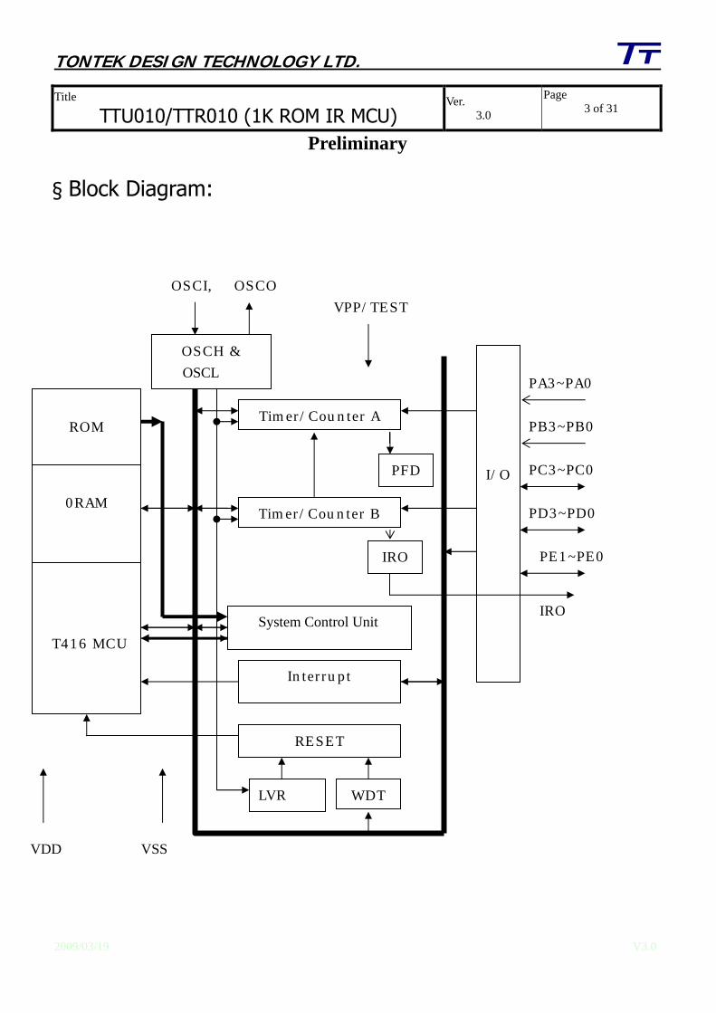
TONTEK DESIGN TECHNOLOGY LTD. Title TTU010/TTR010 (1K ROM IR MCU) Ver. 3.0 Page 1 of 31 Preliminary 2009/03/19 V3.0 TTU010 / TTR010 (IR remote 1K MCU) § General Description: TTU10/TTR010 MCU is an easy-used 4-bit CPU base microcontroller. It contains 1K-word ROM、48-nibble RAM、timer/Counter、interrupt service 、IO control hardware、 carrier generation timer which is especially designed for infrared remote appliance. § Features: 1. Tontek RISC 4-bit CPU core 2. Total 24 crucial instructions and two addressing mode 3. Most instructions need 1 word and 1 machine cycle(2 system clocks) except read table instruction(RTB) 4. advance CMOS process 5. Working memory with 1K*16 program ROM and 48*4 SRAM 6. 1-level stacks 7. Operating voltage: 1.8V~3.6V for resonator oscillator (400KHz~4MHz) 8. System operating frequency: (at VDD=3V ) . High speed system oscillator (OSCH): Resonator mode: 400KHz~4MHz for SR010/SU010 .Low speed peripheral oscillator (OSCL): Built-in RC oscillator: 16KHz(typical) 9. Offers 18 general open drain I/O or input pins 8 input port with wakeup function 8 open drain IO port 2 open drain IO port with CMOS/NMOS output option Offering typical 350mA output driver directly drive IR LED 10. Two 8-bit auto-reload timer/counter One special timer for carrier generation(duty & frequency) One standard timer offers interrupt request 11. MCU system protection: Built-in watch dog timer (WDT) circuit Low voltage Reset(LVR) 12. Provides 2 interrupt sources Internal: Timer/counter A & B
Transcript
TONTEK DESIGN TECHNOLOGY LTD. Title
TTU010/TTR010 (1K ROM IR MCU) Ver. 3.0
Page 1 of 31
Preliminary
2009/03/19 V3.0
TTU010 / TTR010 (IR remote 1K MCU)
§ General Description: TTU10/TTR010 MCU is an easy-used 4-bit CPU base microcontroller. It contains
1K-word ROM、48-nibble RAM、timer/Counter、interrupt service 、IO control hardware、
carrier generation timer which is especially designed for infrared remote appliance.
§ Features: 1. Tontek RISC 4-bit CPU core 2. Total 24 crucial instructions and two addressing mode 3. Most instructions need 1 word and 1 machine cycle(2 system clocks) except read table
instruction(RTB) 4. advance CMOS process 5. Working memory with 1K*16 program ROM and 48*4 SRAM 6. 1-level stacks 7. Operating voltage: 1.8V~3.6V for resonator oscillator (400KHz~4MHz) 8. System operating frequency: (at VDD=3V )
. High speed system oscillator (OSCH): Resonator mode: 400KHz~4MHz for SR010/SU010
9. Offers 18 general open drain I/O or input pins 8 input port with wakeup function 8 open drain IO port 2 open drain IO port with CMOS/NMOS output option Offering typical 350mA output driver directly drive IR LED
10. Two 8-bit auto-reload timer/counter One special timer for carrier generation(duty & frequency) One standard timer offers interrupt request
11. MCU system protection: Built-in watch dog timer (WDT) circuit Low voltage Reset(LVR)
12. Provides 2 interrupt sources Internal: Timer/counter A & B
TONTEK DESIGN TECHNOLOGY LTD. Title
TTU010/TTR010 (1K ROM IR MCU) Ver. 3.0
Page 2 of 31
Preliminary
2009/03/19 V3.0
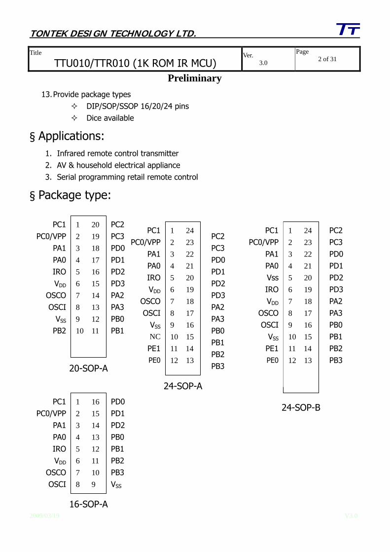
13. Provide package types DIP/SOP/SSOP 16/20/24 pins Dice available
§ Applications: 1. Infrared remote control transmitter 2. AV & household electrical appliance 3. Serial programming retail remote control
§ IO Cell type Description: Pin Name I/O Type Description
PA0~PA3,PB0~PB3 Figure IO-E Input Port PC0~PC3,PD0~PD3, PE0~PE1
Figure IO-F STD open drain IO Port
IRO Figure IO-G STD Output Port
§ Absolute Maximum ratings: ITEM SYMBOL RATING UNIT
Operating Temperature Top -20 ~ +70
Storage Temperature Tst -50 ~ +125
Supply Voltage VDD VSS-0.3 ~VSS+6.0 V
OTP Supply Voltage VPP VSS-0.3 ~ VSS+12.5 V
Input Voltage Vin VSS -0.3 to VDD+0.3 V
Human Body Mode ESD >3 KV
Note: VSS symbolizes for system ground
TONTEK DESIGN TECHNOLOGY LTD. Title
TTU010/TTR010 (1K ROM IR MCU) Ver. 3.0
Page 6 of 31
Preliminary
2009/03/19 V3.0
§ DC Characteristics: (Test condition at room temperature=25oC)
Parameter Symbol Test Condition Min. Typ. Max. UnitOperating Voltage VDD Resonator/Crystal
FOSCH=400K~4MHz1.8 - 3.6 V
Ind1 VDD=3.0V, no load, FOSCH=2MHz,
-
1.0
2.0
Operating Current
(Normal Mode, CPU working,
I/O no load ) Ind3 VDD=3.0V, no load,
FOSCH=455KHz, 0.4 0.7
mA
Standby Current Istb I/O no load, FOSCH & FOSCL stop
-
-
1.0
uA
Input Ports VIL Input Low Voltage 0 - 0.2 VDDInput Ports VIH Input High Voltage 0.8 - 1.0 VDD
PC,PD Sink Current IOL1 VDD=3.0V, Vol=0.6V 2 4 - mAIRO Sink Current IOL2 VDD=3V, VOL=0.6V 300 350 - mA
PD2,PD3 output source current IOH VDD=3.0V, Voh=-0.0V 10 - 30 uA PA,PB pull-high Resistor RPH VDD=3.0V 50 100 150 KΩ Oscillator Start up voltage VST FOSC=455k~2M 1.8 - 2.0 V Oscillator Sustain voltage VSU FOSC=455K~2M 1.3 - 1.5 V
TONTEK DESIGN TECHNOLOGY LTD. Title
TTU010/TTR010 (1K ROM IR MCU) Ver. 3.0
Page 7 of 31
Preliminary
2009/03/19 V3.0
§ AC Characteristics: Parameter Test Condition Min Typ. Max Unit
Wake up input Low active pulse width twkup,
Application de-bounce should be manipulated by user’ software
2 - - OSCL
System Oscillator Frequency
FOSCH(Crystal) VDD=3.0V 400K - 4M Hz
Startup Period of Oscillators
TOSCH (Crystal) wake-up from offmode
- 4 - FOSCH
System Stable Time after Power up
After power up, the system needs to initialize the configured state and
OST.
32 35 40 ms
§ Memory Map:
ROM ADDRESS RAM ADDRESS Function Block
000H~3FFH Program ROM [1K*16]
000H ~ 007H File Registers
008H~01FH Peripheral registers (I)
020H~04FH Working RAM [48*4]
§ Interrupt Vectors: Interrupt Vectors Function Description
$000 hardware RESETB
$001 Hardware IRQB /Soft IRQB
TONTEK DESIGN TECHNOLOGY LTD. Title
TTU010/TTR010 (1K ROM IR MCU) Ver. 3.0
Page 8 of 31
Preliminary
2009/03/19 V3.0
§ File registers: Address Symbol R/W Default Description
000H (DP1) R/W - Indirect addressing register
001H ACC R/W - Accumulator & Read Table 1st data
002H TB1 R/W - Read Table 2nd data
003H TB2 R/W - Read Table 3rd data
004H TB3 R/W - Read Table 4th data
005H DPL R/W - Data Pointer low nibble
006H DPM R/W - Data Pointer middle nibble
007H DPH R/W - Data Pointer high nibble
TONTEK DESIGN TECHNOLOGY LTD. Title
TTU010/TTR010 (1K ROM IR MCU) Ver. 3.0
Page 9 of 31
Preliminary
2009/03/19 V3.0
§ Peripheral registers: Interrupt request flag register Address Symbol R/W Default Description
008H PS R/W 0100 CPU power saving control register
009H INTC R/W 0000 Interrupt enable control register
00AH INTF R/W 0000 Interrupt request flag register
00CH TCPAC W ---- TCPA Timer/counter A control register
00DH TCPAL W 0000 TCPA Timer/counter A data low register
00EH TCPAH W 0000 TCPA Timer/counter A data high register
00FH PA R ---- I/O port A data register
010H PB R ---- I/O port B data register
011H PC R/W 0000 I/O port C data register
012H PD R/W 0000 I/O port D data register
013H TCPBC W ---- TCPB Timer/counter B control register
014H TCPBLL W 0000 TCPB Timer/counter B low data low nibble register
015H TCPBLH W 0000 TCPB Timer/counter B low data high nibble register
016H TCPBHL W 0000 TCPB Timer/counter B high data low nibble register
017H TCPBHH W 0000 TCPB Timer/counter B high data high nibble register
018H PSP R/W ---0 Peripheral power saving control register
019H PE R/W --00 I/O port E data register
Note: a. Default means initial value after power on or reset. b. R is “read” only, W is “write” only, R/W is both of “read” & “write”.
TONTEK DESIGN TECHNOLOGY LTD. Title
TTU010/TTR010 (1K ROM IR MCU) Ver. 3.0
Page 10 of 31
Preliminary
2009/03/19 V3.0
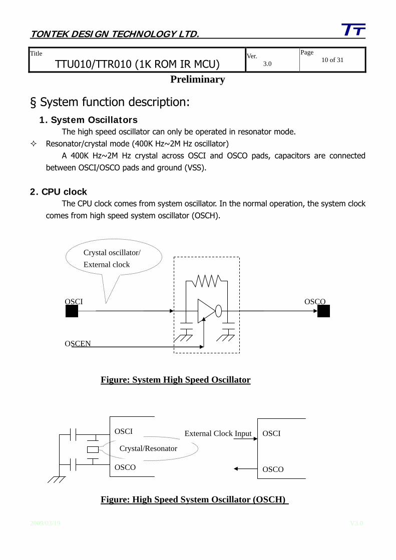
§ System function description: 1. System Oscillators
The high speed oscillator can only be operated in resonator mode. Resonator/crystal mode (400K Hz~2M Hz oscillator)
A 400K Hz~2M Hz crystal across OSCI and OSCO pads, capacitors are connected between OSCI/OSCO pads and ground (VSS).
2. CPU clock The CPU clock comes from system oscillator. In the normal operation, the system clock
comes from high speed system oscillator (OSCH).
OSCO OSCI
Crystal oscillator/ External clock
OSCEN
Figure: System High Speed Oscillator
Crystal/Resonator
OSCO
OSCI External Clock Input
OSCO
OSCI
Figure: High Speed System Oscillator (OSCH)
TONTEK DESIGN TECHNOLOGY LTD. Title
TTU010/TTR010 (1K ROM IR MCU) Ver. 3.0
Page 11 of 31
Preliminary
2009/03/19 V3.0
4. Power saving mode (Stop mode) The CPU enters stop mode is operated by writing CPU power saving register (PS). During the power saving mode, CPU holds the internal status of the system. In stop mode, the oscillator clocks will be stopped and system need a warm-up time for the stability of system clock running after wake up. As system wake up from stop mode will cause a CPU reset. Software program will restart from reset vector.
5. MCU System Operation Modes The MCU has 2 operating modes, including high speed operation, stop modes. After
power on reset, the MCU will go into high speed operation mode automatically. After wake up from stop mode, the MCU will resume the last operation mode.
STOP/ wake up
Reset release
Reset
Reset
STOP mode OSCH off
High speed operating mode
OSCH on
RESET
Figure: System Operation State Diagram
TONTEK DESIGN TECHNOLOGY LTD. Title
TTU010/TTR010 (1K ROM IR MCU) Ver. 3.0
Page 12 of 31
Preliminary
2009/03/19 V3.0
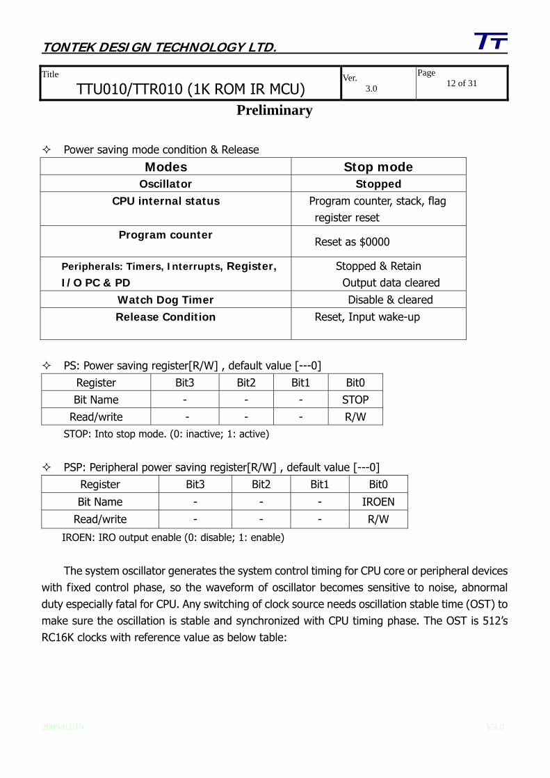
Power saving mode condition & Release
Modes Stop mode Oscillator Stopped
CPU internal status Program counter, stack, flag register reset
Program counter Reset as $0000
Peripherals: Timers, Interrupts, Register, I/O PC & PD
PSP: Peripheral power saving register[R/W] , default value [---0]
Register Bit3 Bit2 Bit1 Bit0
Bit Name - - - IROEN
Read/write - - - R/W
IROEN: IRO output enable (0: disable; 1: enable)
The system oscillator generates the system control timing for CPU core or peripheral devices
with fixed control phase, so the waveform of oscillator becomes sensitive to noise, abnormal duty especially fatal for CPU. Any switching of clock source needs oscillation stable time (OST) to make sure the oscillation is stable and synchronized with CPU timing phase. The OST is 512’s RC16K clocks with reference value as below table:
TONTEK DESIGN TECHNOLOGY LTD. Title
TTU010/TTR010 (1K ROM IR MCU) Ver. 3.0
Page 13 of 31
Preliminary
2009/03/19 V3.0
6 .Interrupts The CPU provides only 1 interrupt vector ($001H) and no priority, but can expand to multi-sources.
Interrupt source includes two timer/counter interrupts (TCPAINT &TCPBINT). The interrupt control
registers (INTC) contain the interrupt control bits to enable and disable corresponding interrupt request
and the corresponding interrupt request flags in the (INTF) registers. Before finishing the INT service
routine, another INT request will keep waiting until program return from interrupt routine.
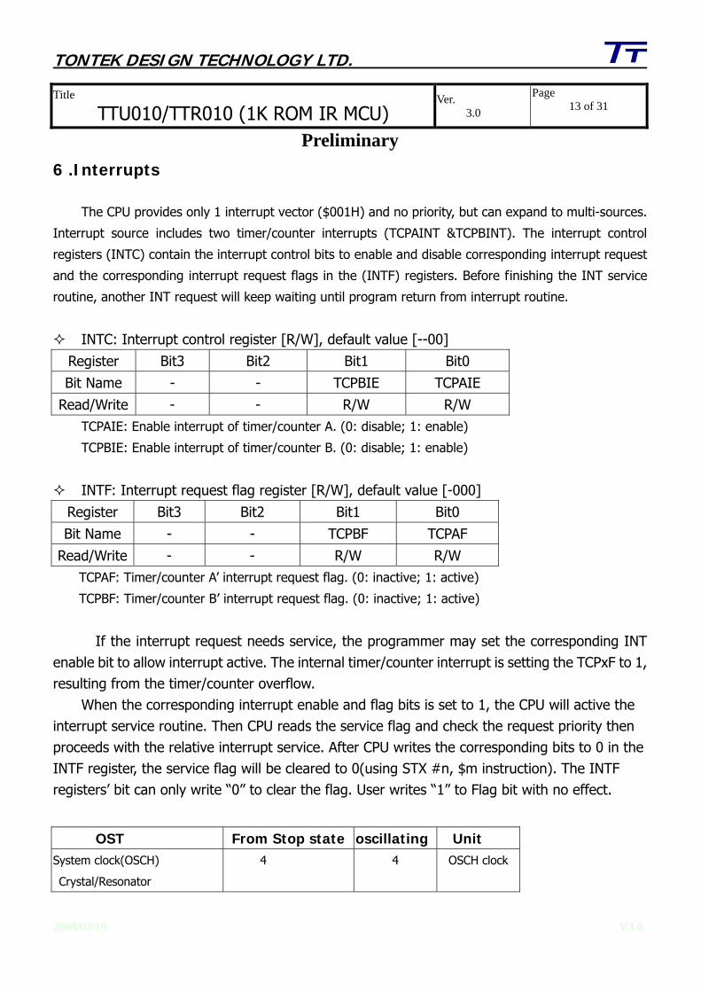
INTC: Interrupt control register [R/W], default value [--00] Register Bit3 Bit2 Bit1 Bit0 Bit Name - - TCPBIE TCPAIE
Read/Write - - R/W R/W TCPAIE: Enable interrupt of timer/counter A. (0: disable; 1: enable)
TCPBIE: Enable interrupt of timer/counter B. (0: disable; 1: enable)
INTF: Interrupt request flag register [R/W], default value [-000] Register Bit3 Bit2 Bit1 Bit0 Bit Name - - TCPBF TCPAF
If the interrupt request needs service, the programmer may set the corresponding INT enable bit to allow interrupt active. The internal timer/counter interrupt is setting the TCPxF to 1, resulting from the timer/counter overflow.
When the corresponding interrupt enable and flag bits is set to 1, the CPU will active the interrupt service routine. Then CPU reads the service flag and check the request priority then proceeds with the relative interrupt service. After CPU writes the corresponding bits to 0 in the INTF register, the service flag will be cleared to 0(using STX #n, $m instruction). The INTF registers’ bit can only write “0” to clear the flag. User writes “1” to Flag bit with no effect.
OST From Stop state oscillating Unit System clock(OSCH)
Crystal/Resonator
4 4 OSCH clock
TONTEK DESIGN TECHNOLOGY LTD. Title
TTU010/TTR010 (1K ROM IR MCU) Ver. 3.0
Page 14 of 31
Preliminary
2009/03/19 V3.0
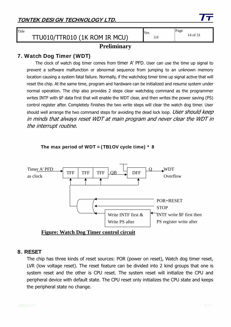
7. Watch Dog Timer (WDT) The clock of watch dog timer comes from timer A’ PFD. User can use the time up signal to
prevent a software malfunction or abnormal sequence from jumping to an unknown memory
location causing a system fatal failure. Normally, if the watchdog timer time up signal active that will
reset the chip. At the same time, program and hardware can be initialized and resume system under
normal operation. The chip also provides 2 steps clear watchdog command as the programmer
writes INTF with $F data first that will enable the WDT clear, and then writes the power saving (PS)
control register after. Completely finishes the two write steps will clear the watch dog timer. User
should well arrange the two command steps for avoiding the dead lock loop. User should keep in minds that always reset WDT at main program and never clear the WDT in the interrupt routine.
The max period of WDT =(TB1OV cycle time) * 8
8. RESET The chip has three kinds of reset sources: POR (power on reset), Watch dog timer reset, LVR (low voltage reset). The reset feature can be divided into 2 kind groups that one is system reset and the other is CPU reset. The system reset will initialize the CPU and peripheral device with default state. The CPU reset only initializes the CPU state and keeps the peripheral state no change.
QQB
WDT Overflow
TFF TFF TFF
POR+RESET STOP INTF write $F first thenPS register write after
DFFTimer A’ PFD as clock
Figure: Watch Dog Timer control circuit
Write INTF first & Write PS after
TONTEK DESIGN TECHNOLOGY LTD. Title
TTU010/TTR010 (1K ROM IR MCU) Ver. 3.0
Page 15 of 31
Preliminary
2009/03/19 V3.0
S-8a System reset
.POR (power on reset)
The chip provides automatic reset function when the power is turned on. The VDD should be below 1.4V and its rising slope (from 0.1VDD up to o.9VDD) needs less than 10ms.
S-8b CPU reset
.Watch Dog Timer Reset
The reset signal will generate automatically when the watchdog timer runs overflow. If the watchdog timer is cleared regularly by user’s program, no watchdog reset will occur. Unless the MCU is forced into abnormal state, the software controlled procedure is disrupted and causing watch dog timer overflow, then it will generate reset signal to initializes the chip returning to normal operation.
. LVR (low voltage reset)
The LVR is a low system voltage detector. As the operating voltage falls below the detected window then the system reset will start the system reset procedure.
For OTP type, hardware needs to down load the mask options into register and the events are caused by power on reset, watch dog overflow reset and LVR reset.
LVR System RESET Detected Vop 0 1 active 1.2V~1.8V 1 0 disable >1.8V
TONTEK DESIGN TECHNOLOGY LTD. Title
TTU010/TTR010 (1K ROM IR MCU) Ver. 3.0
Page 16 of 31
Preliminary
2009/03/19 V3.0
§ Peripheral function description: 1. 8 bits Carrier Timer (TCP) for TCPB
One 8-bits timer (TCP) with system clock source and preload data buffer can implement as a timer, IRO is programmable frequency divider can support IR carrier generator. TCPOV is the timer overflow signal and the rising edge will set the relative INT flag.
TCPC: Timer control register[W], default value [----] Register Bit3 Bit2 Bit1 Bit0
Bit Name - - - -
Read/Write - - - -
As writing the TCPC address, the timer will reload the high latch data into counter that means PFD will be initialized for choosing high latch data.
TCPDLL: TCP low nibble for low data register[R/W], default value [0000] Register Bit3 Bit2 Bit1 Bit0
Bit Name TCPDL3 TCPDL2 TCPDL1 TCPDL0
Read/Write W W W W
TCPD3~TCPD0: TCPD low nibble of data buffer. TCPDLH: TCP high nibble for low data register[R/W], default value [0000]
Register Bit3 Bit2 Bit1 Bit0
Bit Name TCPDL7 TCPDL6 TCPDL5 TCPDL4
Read/Write W W W W
TCPD7~TCPD4: TCPD high nibble of data buffer. TCPDHL: TCP low nibble for high data register[R/W], default value [0000]
Register Bit3 Bit2 Bit1 Bit0
Bit Name TCPDH3 TCPDH2 TCPDH1 TCPDH0
Read/Write W W W W
TCPDH3~TCPDH0: TCPDH low nibble of data buffer. TCPDHH: TCP high nibble for high data register[R/W], default value [0000]
Register Bit3 Bit2 Bit1 Bit0
Bit Name TCPDH7 TCPDH6 TCPDH5 TCPDH4
Read/Write W W W W
TCPDH7~TCPDH4: TCPDH high nibble of data buffer.
TONTEK DESIGN TECHNOLOGY LTD. Title
TTU010/TTR010 (1K ROM IR MCU) Ver. 3.0
Page 17 of 31
Preliminary
2009/03/19 V3.0
TCPDL: Like a 8 bit TCP low data register, default value [00H] TCPDL Bit7 Bit6 Bit5 Bit4 Bit3 Bit2 Bit1 Bit0
Bit Name TCPDL7 TCPDL6 TCPDL5 TCPDL4 TCPDL3 TCPDL2 TCPDL1 TCPDL0
TCPDH: Like a 8 bit TCP high data register, default value [00H] TCPDH Bit7 Bit6 Bit5 Bit4 Bit3 Bit2 Bit1 Bit0
Bit Name TCPDH7 TCPDH6 TCPDH5 TCPDH4 TCPDH3 TCPDH2 TCPDH1 TCPDH0
.Timer When TCP works as a Timer, user needs give the preload data TCPDH (output high
level)/TCPDL (output low level) for periodic waveform generation. After initial setting, user starts the TCP counting by setting TCPEN=1, the TCP cycle period is:
Tc = (selected clock cycle) * (TCPDH+TCPDL) When user writes data to the TCPDH & TCPDL, the data just keep in TCPDxL/H register.
During the TCPEN=1 command executed, the TCPD 1’s complement value will load the TCPDHx into counter TCP as initial value and start the timer function. Necessary keeps in auto reload mode, timer run with reload feature as TCP up counts and reaches the value 0f “FFH” or 255. The next reload data is TCPDLx for carrier low level. The procedure keeps alternately and Infrared carrier generation & PWM output are easily implemented.
TONTEK DESIGN TECHNOLOGY LTD. Title
TTU010/TTR010 (1K ROM IR MCU) Ver. 3.0
Page 18 of 31
Preliminary
2009/03/19 V3.0
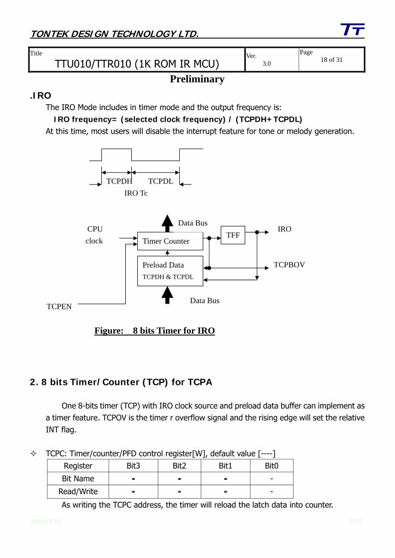
.IRO The IRO Mode includes in timer mode and the output frequency is: IRO frequency= (selected clock frequency) / (TCPDH+TCPDL) At this time, most users will disable the interrupt feature for tone or melody generation.
2. 8 bits Timer/Counter (TCP) for TCPA
One 8-bits timer (TCP) with IRO clock source and preload data buffer can implement as a timer feature. TCPOV is the timer r overflow signal and the rising edge will set the relative INT flag.
TCPC: Timer/counter/PFD control register[W], default value [----]
Register Bit3 Bit2 Bit1 Bit0
Bit Name - - - -
Read/Write - - - -
As writing the TCPC address, the timer will reload the latch data into counter.
IRO
TCPBOV
CPU clock Timer Counter
TFF
Preload Data TCPDH & TCPDL
Data Bus
Data Bus
Figure: 8 bits Timer for IRO
TCPEN
TCPDH TCPDL IRO Tc
TONTEK DESIGN TECHNOLOGY LTD. Title
TTU010/TTR010 (1K ROM IR MCU) Ver. 3.0
Page 19 of 31
Preliminary
2009/03/19 V3.0
TCPDL: TCP low nibble data register[W], default value [0000] Register Bit3 Bit2 Bit1 Bit0
Bit Name TCPD3 TCPD2 TCPD1 TCPD0
Read/Write W W W W
TCPD3~TCPD0:TCPD low nibble of data buffer.
TCPDH: TCP high nibble data register[W], default value [0000] Register Bit3 Bit2 Bit1 Bit0
Bit Name TCPD7 TCPD6 TCPD5 TCPD4
Read/Write W W W W
TCPD7~TCPD4: TCPD high nibble of data buffer. TCPD: Like a 8 bit TCP data register[W], default value [00H] Register Bit7 Bit6 Bit5 Bit4 Bit3 Bit2 Bit1 Bit0
Bit Name TCPD7 TCPD6 TCPD5 TCPD4 TCPD3 TCPD2 TCPD1 TCPD0 Read/Write
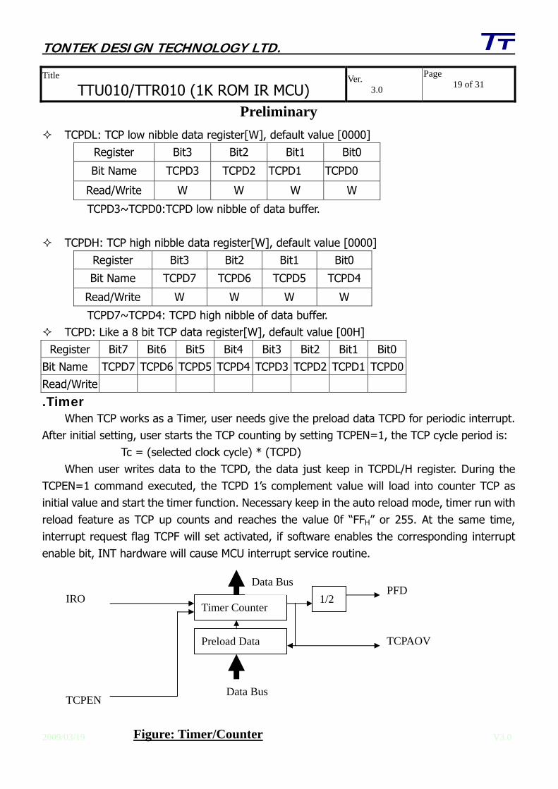
.Timer When TCP works as a Timer, user needs give the preload data TCPD for periodic interrupt.
After initial setting, user starts the TCP counting by setting TCPEN=1, the TCP cycle period is: Tc = (selected clock cycle) * (TCPD) When user writes data to the TCPD, the data just keep in TCPDL/H register. During the
TCPEN=1 command executed, the TCPD 1’s complement value will load into counter TCP as initial value and start the timer function. Necessary keep in the auto reload mode, timer run with reload feature as TCP up counts and reaches the value 0f “FFH” or 255. At the same time, interrupt request flag TCPF will set activated, if software enables the corresponding interrupt enable bit, INT hardware will cause MCU interrupt service routine.
PFD
TCPAOV
Timer Counter 1/2
Preload Data
Data Bus
Data Bus
Figure: Timer/Counter
TCPEN
IRO
TONTEK DESIGN TECHNOLOGY LTD. Title
TTU010/TTR010 (1K ROM IR MCU) Ver. 3.0
Page 20 of 31
Preliminary
2009/03/19 V3.0
.. IO Pad Cells The main features of pad cell are including ESD/EFT protection and general I/O access. An
open drain I/O pad cell can be used as input with or without pull-up resistor, or working as a CMOS or NMOS output driver. The input pad cell must have pull-up resistor for avoiding a floating state when user doesn’t care or not be used. For concerning the standby current, user can use data register or I/O control register to fit the application.
. I/O File Register PA: Port A input port [R], default value [----]
Register Bit3 Bit2 Bit1 Bit0Bit Name PA3 PA2 PA1 PA0
Read/Write R R R R PA3~PA0: port A’ input port.
PB: Port B input port [R], default value [----] Register Bit3 Bit2 Bit1 Bit0
Bit Name PB3 PB2 PB1 PB0
Read/Write R R R R
PB3~PB0: port B input port. PC: Port C data register [R/W], default value [0000]
Register Bit3 Bit2 Bit1 Bit0 Bit Name PC3 PC2 PC1 PC0
Read/Write R/W R/W R/W R/W
PC3~PC0: port C data register NMOS output only. PD: Port D data register [R/W], default value [0000]
Register Bit3 Bit2 Bit1 Bit0 Bit Name PD3 PD2 PD1 PD0
Read/Write R/W R/W R/W R/W PD1~PD0: port D data register. NMOS output only PD3~PD2: port D data register. With CMOS or NMOS output optional.
PE: Port E data register [R/W], default value [--00] Register Bit3 Bit2 Bit1 Bit0 Bit Name - - PE1 PE0
Read/Write - - R/W R/W PE1~PE0: port E data register NMOS output only.
TONTEK DESIGN TECHNOLOGY LTD. Title
TTU010/TTR010 (1K ROM IR MCU) Ver. 3.0
Page 21 of 31
Preliminary
2009/03/19 V3.0
. I/O PAD Cell Structure & Function Description
.. Input Port The input port always has the pull high resistor and input data can read by port
reading command. A wake-up function also offers the system wake up feature for keys or special external triggers.
Input Data Read Data Wake-up
0 0 Active 1 1 Non-active
Floating 1 Non-active
PAD (PA, PB)
Figure IO-E: Input Port
Pull-High R
Data
Wake-up
Read
P
TONTEK DESIGN TECHNOLOGY LTD. Title
TTU010/TTR010 (1K ROM IR MCU) Ver. 3.0
Page 22 of 31
Preliminary
2009/03/19 V3.0
.. Output Port The output driver has drive capability for heavy load. The output enable option is a control signal for disable output feature and pad can release to use as input or another request.
Internal signal Data Output option enable PAD Data x disable Floating 0 enable 0 1 enable 1
.. Standard open drain IO Port The standard open drain IO port has no I/O control register for switching input or output
mode and use output data register to change the IO mode. If output data=1, the I/O port is programmed as input with pull-up resister or not dependant on CMOS type or NMOS type output.
Note: In the STOP mode IO port data register will be cleared that is for key scan with wake up feature.
Output Type Output Register data PAD data Pull-up CMOS 0 0 No CMOS 1 Input mode Yes NMOS 0 0 No NMOS 1 Input mode No
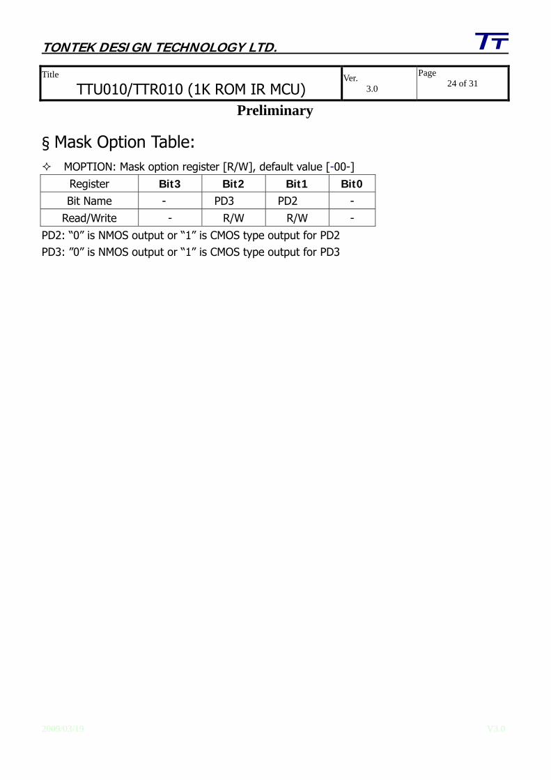
Read/Write - R/W R/W - PD2: “0” is NMOS output or “1” is CMOS type output for PD2 PD3: ”0” is NMOS output or “1” is CMOS type output for PD3
TONTEK DESIGN TECHNOLOGY LTD. Title
TTU010/TTR010 (1K ROM IR MCU) Ver. 3.0
Page 25 of 31
Preliminary
2009/03/19 V3.0
§ Package & PAD Information: 20-SOP
24-SOP
TONTEK DESIGN TECHNOLOGY LTD. Title
TTU010/TTR010 (1K ROM IR MCU) Ver. 3.0
Page 26 of 31
Preliminary
2009/03/19 V3.0
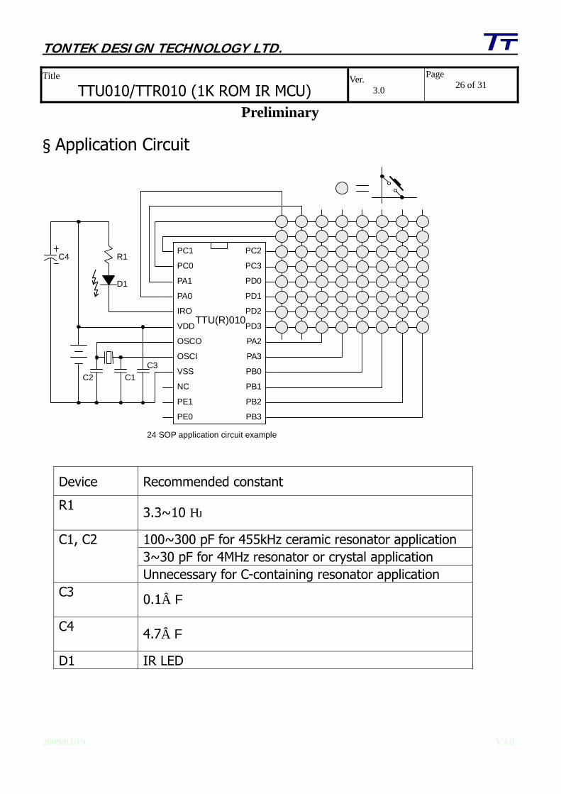
§ Application Circuit
TTU(R)010
R1
D1
C3 C1 C2
C4 PC2
PC3
PD0
PD1
PD2
PD3
PA2
PA3
PB0
PB1
PB2
PB3
PC1
PC0
PA1
PA0
IRO
VDD
OSCO
OSCI
VSS
NC
PE1
PE0
24 SOP application circuit example
Device Recommended constant
R1 3.3~10 Ω
100~300 pF for 455kHz ceramic resonator application 3~30 pF for 4MHz resonator or crystal application
C1, C2
Unnecessary for C-containing resonator application C3 0.1μF
C4 4.7μF
D1 IR LED
TONTEK DESIGN TECHNOLOGY LTD. Title
TTU010/TTR010 (1K ROM IR MCU) Ver. 3.0
Page 27 of 31
Preliminary
2009/03/19 V3.0
PC1
PC0
PA1
PA0
IRO
VDD
OSCO
OSCI
VSS
PA6
PC2
PC3
PD0
PD1
PD2
PD3
PA2
PA3
PB0
PB1
TTU(R)010
R1
D1
C3 C1 C2
C4
20 SOP application circuit example
Device Recommended constant
R1 3.3~10 Ω
100~300 pF for 455kHz ceramic resonator application 3~30 pF for 4MHz resonator or crystal application
C1, C2
Unnecessary for C-containing resonator application C3 0.1μF
C4 4.7μF
D1 IR LED
TONTEK DESIGN TECHNOLOGY LTD. Title
TTU010/TTR010 (1K ROM IR MCU) Ver. 3.0
Page 28 of 31
Preliminary
2009/03/19 V3.0
TTU(R)010
R1
D1
C3 C1 C2
C4
DICE application circuit example
PA1
PA0
IRO
OSCI
OSCO
PC0PC1PC2PC3
VDD
VSSPE1PE0PB3PB2
PD0
PD1
PD2
PD3
PA2
PA3
PB1
PB0
Device Recommended constant
R1 3.3~10 Ω
100~300 pF for 455kHz ceramic resonator application 3~30 pF for 4MHz resonator or crystal application
C1, C2
Unnecessary for C-containing resonator application C3 0.1μF
C4 4.7μF
D1 IR LED
TONTEK DESIGN TECHNOLOGY LTD. Title
TTU010/TTR010 (1K ROM IR MCU) Ver. 3.0
Page 29 of 31
Preliminary
2009/03/19 V3.0
§Appendix: For the remote control application, the IR transmission may cause the variations in current
from a few hundred uA to a few hundred mA. This current variation will generate overshoot and undershoot noise on the power line to cause the system malfunction.
To reduce the noise and stabilize the operation of the chip, we recommend the application designer design the PCB for the remote controller as follows to reduce the overshoot and undershoot of the IR LED drive current.
Oscillator circuit (resonator & capacitors) should be located as near as possible to
the chip PCB pattern for VDD & VSS should be as wide and short as possible IR LED should be located as far as possible from the chip Power supply battery and power capacitor (0.1uF & 47uF) should be located as
near as possible to the chip The VDD pattern of the IR LED and the power pins of the chip (VDD & VSS) should be
separated and connected directly with the battery terminal The power capacitors (0.1uF & 47uF) is recommend to reduce the noise Keeping substrate floating and L/F pad connects to VSS power line in dice form The recommended R1/R2 is 15Ω
TONTEK DESIGN TECHNOLOGY LTD. Title
TTU010/TTR010 (1K ROM IR MCU) Ver. 3.0
Page 30 of 31
Preliminary
2009/03/19 V3.0
Recommended PCB layout for dice
C6
C8
C7
C5
X2
D2
R2
OSCO
OSCI
455K
Vss
VDD
IRO
300P
300P
4.7uF
0.1uF
IR LED
--Battery --
+Battery +
Recommended PCB layout for package
C2
C4
C3
C1
X1
D1
R1
815 16 17 18 19 20 21 22 232412
3
4
5
6
7
1411 13
109
300P
300P
4.7uF
0.1uF
IR LED
455K-- Battery --
OSCO
L/F PAD
PC2
PE1
VSSOSCI
IRO
PA0
PA1PC1PC0
VDD
+ Battery + PC3 PD0
PD1 PD2 PD3 PA2 PA3 PB0 PB1
PB2PB312PE0
TONTEK DESIGN TECHNOLOGY LTD. Title
TTU010/TTR010 (1K ROM IR MCU) Ver. 3.0
Page 31 of 31
Preliminary
2009/03/19 V3.0
§ Ordering Form: a. Package form : TTU(R)010-zzz
b. Chip form : TCU(R)010-zzz c. Wafer base : TDU(R)010-zzz