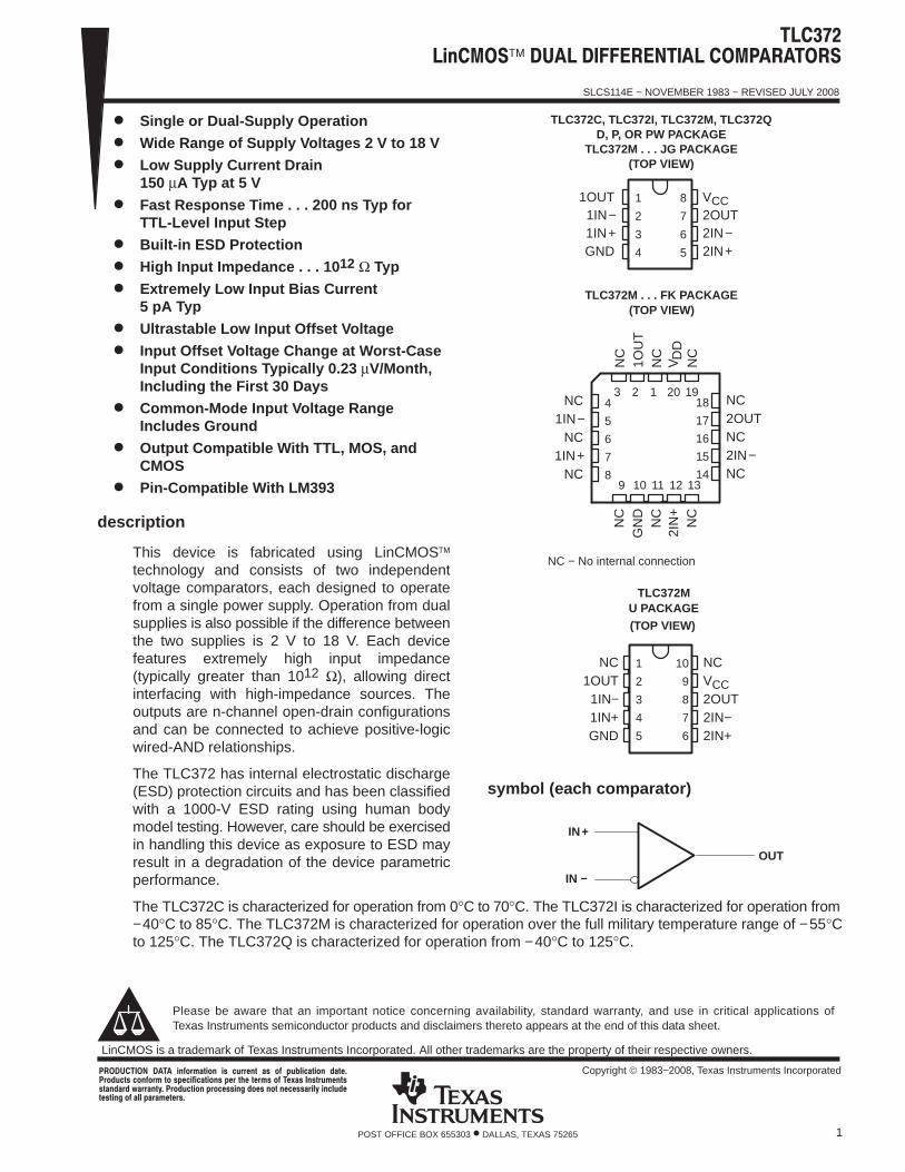
TLC372 LinCMOSDUAL DIFFERENTIAL COMPARATORS SLCS114E - NOVEMBER 1983 - REVISED JULY 2008 1 POST OFFICE BOX 655303 • DALLAS, TEXAS 75265 D Single or Dual-Supply Operation D Wide Range of Supply Voltages 2 V to 18 V D Low Supply Current Drain 150 µA Typ at 5 V D Fast Response Time . . . 200 ns Typ for TTL-Level Input Step D Built-in ESD Protection D High Input Impedance . . . 10 12 Ω Typ D Extremely Low Input Bias Current 5 pA Typ D Ultrastable Low Input Offset Voltage D Input Offset Voltage Change at Worst-Case Input Conditions Typically 0.23 µV/Month, Including the First 30 Days D Common-Mode Input Voltage Range Includes Ground D Output Compatible With TTL, MOS, and CMOS D Pin-Compatible With LM393 description This device is fabricated using LinCMOStechnology and consists of two independent voltage comparators, each designed to operate from a single power supply. Operation from dual supplies is also possible if the difference between the two supplies is 2 V to 18 V. Each device features extremely high input impedance (typically greater than 10 12 Ω), allowing direct interfacing with high-impedance sources. The outputs are n-channel open-drain configurations and can be connected to achieve positive-logic wired-AND relationships. The TLC372 has internal electrostatic discharge (ESD) protection circuits and has been classified with a 1000-V ESD rating using human body model testing. However, care should be exercised in handling this device as exposure to ESD may result in a degradation of the device parametric performance. The TLC372C is characterized for operation from 0°C to 70°C. The TLC372I is characterized for operation from -40°C to 85°C. The TLC372M is characterized for operation over the full military temperature range of - 55°C to 125°C. The TLC372Q is characterized for operation from - 40°C to 125°C. Please be aware that an important notice concerning availability, standard warranty, and use in critical applications of Texas Instruments semiconductor products and disclaimers thereto appears at the end of this data sheet. Copyright 1983-2008, Texas Instruments Incorporated PRODUCTION DATA information is current as of publication date. Products conform to specifications per the terms of Texas Instruments standard warranty. Production processing does not necessarily include testing of all parameters. 1 2 3 4 8 7 6 5 1OUT 1IN- 1IN+ GND V CC 2OUT 2IN- 2IN+ TLC372C, TLC372I, TLC372M, TLC372Q D, P, OR PW PACKAGE TLC372M . . . JG PACKAGE (TOP VIEW) 3 2 1 20 19 9 10 11 12 13 4 5 6 7 8 18 17 16 15 14 NC 2OUT NC 2IN- NC NC 1IN- NC 1IN+ NC TLC372M . . . FK PACKAGE (TOP VIEW) NC 1OUT NC 2IN+ NC NC NC GND NC OUT IN+ symbol (each comparator) IN - NC - No internal connection V DD 1 2 3 4 5 10 9 8 7 6 NC 1OUT 1IN- 1IN+ GND NC V CC 2OUT 2IN- 2IN+ TLC372M U PACKAGE (TOP VIEW) LinCMOS is a trademark of Texas Instruments Incorporated. All other trademarks are the property of their respective owners.
Transcript
SLCS114E − NOVEMBER 1983 − REVISED JULY 2008
1POST OFFICE BOX 655303 • DALLAS, TEXAS 75265
Single or Dual-Supply Operation
Wide Range of Supply Voltages 2 V to 18 V
Low Supply Current Drain 150 µA Typ at 5 V
Fast Response Time . . . 200 ns Typ for TTL-Level Input Step
Built-in ESD Protection
High Input Impedance . . . 1012 Ω Typ
Extremely Low Input Bias Current 5 pA Typ
Ultrastable Low Input Offset Voltage
Input Offset Voltage Change at Worst-CaseInput Conditions Typically 0.23 µV/Month,Including the First 30 Days
Common-Mode Input Voltage RangeIncludes Ground
Output Compatible With TTL, MOS, and CMOS
Pin-Compatible With LM393
description
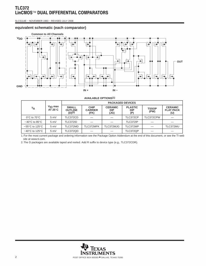
This device is fabricated using LinCMOStechnology and consists of two independentvoltage comparators, each designed to operatefrom a single power supply. Operation from dualsupplies is also possible if the difference betweenthe two supplies is 2 V to 18 V. Each devicefeatures extremely high input impedance(typically greater than 1012 Ω), allowing directinterfacing with high-impedance sources. Theoutputs are n-channel open-drain configurationsand can be connected to achieve positive-logicwired-AND relationships.
The TLC372 has internal electrostatic discharge(ESD) protection circuits and has been classifiedwith a 1000-V ESD rating using human bodymodel testing. However, care should be exercisedin handling this device as exposure to ESD mayresult in a degradation of the device parametricperformance.
The TLC372C is characterized for operation from 0°C to 70°C. The TLC372I is characterized for operation from−40°C to 85°C. The TLC372M is characterized for operation over the full military temperature range of −55°Cto 125°C. The TLC372Q is characterized for operation from −40°C to 125°C.
Please be aware that an important notice concerning availability, standard warranty, and use in critical applications ofTexas Instruments semiconductor products and disclaimers thereto appears at the end of this data sheet.
1.For the most current package and ordering information see the Package Option Addendum at the end of this document, or see the TI website at www.ti.com.
2.The D packages are available taped and reeled. Add R suffix to device type (e.g., TLC372CDR).
SLCS114E − NOVEMBER 1983 − REVISED JULY 2008
3POST OFFICE BOX 655303 • DALLAS, TEXAS 75265
absolute maximum ratings over operating free-air temperature range (unless otherwise noted) †
Storage temperature range −65°C to 150°C. . . . . . . . . . . . . . . . . . . . . . . . . . . . . . . . . . . . . . . . . . . . . . . . . . . . . . . . Case temperature for 60 seconds: FK package 260°C. . . . . . . . . . . . . . . . . . . . . . . . . . . . . . . . . . . . . . . . . . . . . . Lead temperature 1,6 mm (1/16 inch) from case for 10 seconds: D, P, or PW package 260°C. . . . . . . . . . . . Lead temperature 1,6 mm (1/16 inch) from case for 60 seconds: JG or U package 300°C. . . . . . . . . . . . . . .
† Stresses beyond those listed under “absolute maximum ratings” may cause permanent damage to the device. These are stress ratings only, andfunctional operation of the device at these or any other conditions beyond those indicated under “recommended operating conditions” is notimplied. Exposure to absolute-maximum-rated conditions for extended periods may affect device reliability.
NOTES: 3. All voltage values except differential voltages are with respect to network ground.4. Differential voltages are at IN+ with respect to IN −.5. Short circuits from outputs to VDD can cause excessive heating and eventual device destruction.6. Maximum power dissipation is a function of TJ(max), θJA, and TA. The maximum allowable power dissipation at any allowable
ambient temperature is PD = (TJ(max) − TA)/θJA. Operating at the absolute maximum TJ of 150°C can affect reliability.7. The package thermal impedance is calculated in accordance with JESD 51-7 (plastic) or MIL-STD-883 Method 1012 (ceramic).
Operating free-air temperature, TA 0 70 −40 85 −55 125 −40 125 °C
SLCS114E − NOVEMBER 1983 − REVISED JULY 2008
Template Release Date: 7−11−94
****
4 POST OFFICE BOX 655303 DALLAS, TEXAS 75265•
elec
tric
al c
hara
cter
istic
s at
spe
cifie
d fr
ee-a
ir te
mpe
ratu
re, V
DD
= 5
V (
unle
ss o
ther
wis
e no
ted)
PA
RA
ME
TE
RT
ES
T C
ON
DIT
ION
ST A
†T
LC37
2CT
LC37
2IT
LC37
2M, T
LC37
2QU
NIT
PA
RA
ME
TE
RT
ES
T C
ON
DIT
ION
ST A
†M
INT
YP
MA
XM
INT
YP
MA
XM
INT
YP
MA
XU
NIT
VIO
Inpu
t offs
et v
olta
geV
IC =
VIC
Rm
in,
See
Not
e 4
25°C
15
15
15
mV
VIO
Inpu
t offs
et v
olta
geV
IC =
VIC
Rm
in,
See
Not
e 4
Ful
l ran
ge6.
57
10m
V
I IOIn
put o
ffset
cur
rent
25°C
11
1pA
I IOIn
put o
ffset
cur
rent
MA
X0.
31
10nA
I IBIn
put b
ias
curr
ent
25°C
55
5pA
I IBIn
put b
ias
curr
ent
MA
X0.
62
20nA
VIC
RC
omm
on-m
ode
inpu
t25
°C
0 to
VD
D−
1
0 to
VD
D−
1
0 to
VD
D−
1V
VIC
RC
omm
on-m
ode
inpu
tvo
ltage
ran
geF
ull r
ange
0
toV
DD
−1.
5
0 to
VD
D−
1.5
0
toV
DD
−1.
5
V
I OH
Hig
h-le
vel o
utpu
t cur
rent
VID
= 1
VV
OH
= 5
V25
°C0.
10.
10.
1nA
I OH
Hig
h-le
vel o
utpu
t cur
rent
VID
= 1
VV
OH
= 1
5 V
Ful
l ran
ge1
13
µA
VO
LLo
w-le
vel o
utpu
t vol
tage
VID
= −
1 V,
I OL
= 4
mA
25°C
150
400
150
400
150
400
mV
VO
LLo
w-le
vel o
utpu
t vol
tage
VID
= −
1 V,
I OL
= 4
mA
Ful
l ran
ge70
070
070
0m
V
I OL
Low
-leve
l out
put c
urre
ntV
ID =
−1
V,V
OL
= 1
.5 V
25°C
616
616
616
mA
I DD
Sup
ply
curr
ent
VID
= 1
V,
No
load
25°C
150
300
150
300
150
300
µAI D
DS
uppl
y cu
rren
t(t
wo
com
para
tors
)V
ID =
1 V
,N
o lo
adF
ull r
ange
400
400
400
µA
†A
ll ch
arac
teris
tics
are
mea
sure
d w
ith z
ero
com
mon
-mod
e in
put v
olta
ge u
nles
s ot
herw
ise
note
d. F
ull r
ange
is 0
°C to
70°
C fo
r T
LC37
2C, −
40°C
to 8
5°C
for
TLC
372I
, and
−55
°C to
125°
C fo
r T
LC37
2M a
nd −
40°C
to 1
25°C
for
TLC
372Q
. IM
PO
RTA
NT:
See
Par
amet
er M
easu
rem
ent I
nfor
mat
ion.
NO
TE
8:
The
offs
et v
olta
ge li
mits
giv
en a
re th
e m
axim
um v
alue
s re
quire
d to
driv
e th
e ou
tput
abo
ve 4
V o
r bel
ow 4
00 m
V w
ith a
10-
kΩ r
esis
tor
betw
een
the
outp
ut a
nd V
DD
. The
y ca
nbe
ver
ified
by
appl
ying
the
limit
valu
e to
the
inpu
t and
che
ckin
g fo
r th
e ap
prop
riate
out
put s
tate
.
switc
hing
cha
ract
eris
tics,
VD
D =
5 V
, TA
= 2
5°C
PA
RA
ME
TE
RT
ES
T C
ON
DIT
ION
SM
INT
YP
MA
XU
NIT
Res
pons
e tim
eR
L co
nnec
ted
to 5
V th
roug
h 5.
1 kΩ
,C
L =
15
pF‡ ,
10
0-m
V in
put s
tep
with
5-m
V o
verd
rive
650
nsR
espo
nse
time
RL
conn
ecte
d to
5 V
thro
ugh
5.1
kΩ,
CL
= 1
5 pF
‡ ,
See
Not
e 5
TT
L-le
vel i
nput
ste
p20
0ns
‡C
L in
clud
es p
robe
and
jig
capa
cita
nce.
NO
TE
9:
The
res
pons
e tim
e sp
ecifi
ed is
the
inte
rval
bet
wee
n th
e in
put s
tep
func
tion
and
the
inst
ant w
hen
the
outp
ut c
ross
es 1
.4 V
.
SLCS114E − NOVEMBER 1983 − REVISED JULY 2008
5POST OFFICE BOX 655303 • DALLAS, TEXAS 75265
electrical characteristics at specified free-air temperature, V DD = 5 V, TA = 25°C (unless otherwisenoted)
PARAMETER TEST CONDITIONS†TLC372Y
UNITPARAMETER TEST CONDITIONS†MIN TYP MAX
UNIT
VIO Input offset voltage VIC = VICRmin, See Note 4 1 5 mV
IIO Input offset current 1 pA
IIB Input bias current 5 pA
VICR Common-mode input voltage range 0 toVDD−1 V
IOH High-level output current VID = 1 V, VOH = 5 V 0.1 nA
VOL Low-level output voltage VID = −1 V, IOL = 4 mA 150 400 mV
IOL Low-level output current VID = −1 V, VOL = 1.5 V 6 16 mA
IDD Supply current (two comparators) VID = 1 V, No load 150 300 µA
† All characteristics are measured with zero common-mode input voltage unless otherwise noted. IMPORTANT: See Parameter MeasurementInformation.
NOTE 4: The offset voltage limits given are the maximum values required to drive the output above 4 V or below 400 mV with a 10-kΩ resistorbetween the output and VDD. They can be verified by applying the limit value to the input and checking for the appropriate output state.
PARAMETER MEASUREMENT INFORMATION
The digital output stage of the TLC372 can be damaged if it is held in the linear region of the transfer curve.Conventional operational amplifier/comparator testing incorporates the use of a servo loop that is designed to forcethe device output to a level within this linear region. Since the servo-loop method of testing cannot be used, thefollowing alternatives for measuring parameters such as input offset voltage, common-mode rejection, etc., areoffered.
To verify that the input offset voltage falls within the limits specified, the limit value is applied to the input as shownin Figure 1(a). With the noninverting input positive with respect to the inverting input, the output should be high. Withthe input polarity reversed, the output should be low.
A similar test can be made to verify the input offset voltage at the common-mode extremes. The supply voltages canbe slewed as shown in Figure 1(b) for the VICR test, rather than changing the input voltages, to provide greateraccuracy.
5 V
5.1 kΩ
VO
Applied V IOLimit
VO
5.1 kΩ
1 V
−4 V
−
+
−
+
(a) VIO WITH VIC = 0 (b) VIO WITH VIC = 4 V
Applied V IOLimit
Figure 1. Method for Verifying That Input Offset Voltage is Within Specified Limits
SLCS114E − NOVEMBER 1983 − REVISED JULY 2008
6 POST OFFICE BOX 655303 • DALLAS, TEXAS 75265
PARAMETER MEASUREMENT INFORMATION
A close approximation of the input offset voltage can be obtained by using a binary search method to vary thedifferential input voltage while monitoring the output state. When the applied input voltage differential is equal, butopposite in polarity, to the input offset voltage, the output changes states.
Figure 2 illustrates a practical circuit for direct dc measurement of input offset voltage that does not bias thecomparator into the linear region. The circuit consists of a switching-mode servo loop in which U1a generates atriangular waveform of approximately 20-mV amplitude. U1b acts as a buffer, with C2 and R4 removing any residualdc offset. The signal is then applied to the inverting input of the comparator under test, while the noninverting inputis driven by the output of the integrator formed by U1c through the voltage divider formed by R9 and R10. The loopreaches a stable operating point when the output of the comparator under test has a duty cycle of exactly 50%, whichcan only occur when the incoming triangle wave is sliced symmetrically or when the voltage at the noninverting inputexactly equals the input offset voltage.
Voltage divider R9 and R10 provides a step up of the input offset voltage by a factor of 100 to make measurementeasier. The values of R5, R8, R9, and R10 can significantly influence the accuracy of the reading; therefore, it issuggested that their tolerance level be 1% or lower.
Measuring the extremely low values of input current requires isolation from all other sources of leakage current andcompensation for the leakage of the test socket and board. With a good picoammeter, the socket and board leakagecan be measured with no device in the socket. Subsequently, this open-socket leakage value can be subtracted fromthe measurement obtained with a device in the socket to obtain the actual input current of the device.
R65.1 kΩBuffer
U1b1/4 TLC274C
R1240 kΩ
C21 µF
R447 kΩ
U1a1/4 TLC274CN
U1c1/4 TLC274CN
R210 kΩR3
100 kΩ
C10.1 µF
R10100 Ω, 1%
R910 kΩ, 1%
R71 MΩ
R81.8 kΩ, 1%
R51.8 kΩ, 1%
VDD
DUT
Integrator
VIO(X100)
C30.68 µF
C40.1 µF
TriangleGenerator
−
+
−
+
−
+
Figure 2. Circuit for Input Offset Voltage Measurement
SLCS114E − NOVEMBER 1983 − REVISED JULY 2008
7POST OFFICE BOX 655303 • DALLAS, TEXAS 75265
PARAMETER MEASUREMENT INFORMATION
Response time is defined as the interval between the application of an input step function and the instant when theoutput reaches 50% of its maximum value. Response time, low-to-high level output, is measured from the leadingedge of the input pulse, while response time, high-to-low level output, is measured from the trailing edge of the inputpulse. Response-time measurement at low input signal levels can be greatly affected by the input offset voltage. Theoffset voltage should be balanced by the adjustment at the inverting input as shown in Figure 3, so that the circuitis just at the transition point. Then a low signal, for example 105-mV or 5-mV overdrive, causes the output to changestate.
ÁÁÁLow-to-High-Level Output
DUT
5.1 kΩ 1 µF
0.1 µF
1 kΩ
50 Ω
CL(see Note A)
VDD
PulseGenerator
Input Offset VoltageCompensation Adjustment
10 Ω10 Turn
1 V
−1 V
Overdrive
Input
100 mV
Overdrive
Input
tftPHL
10%
50%
90%90%
50%
trtPLH
High-to-Low-Level Output
TEST CIRCUIT
VOLTAGE WAVEFORMS
10%
100 mV
NOTE A: CL includes probe and jig capacitance.
Figure 3. Response, Rise, and Fall Times Circuit and Voltage Waveforms
SLCS114E − NOVEMBER 1983 − REVISED JULY 2008
8 POST OFFICE BOX 655303 • DALLAS, TEXAS 75265
PRINCIPLES OF OPERATION
LinCMOS process
The LinCMOS process is a Linear polysilicon-gate complementary-MOS process. Primarily designed forsingle-supply applications, LinCMOS products facilitate the design of a wide range of high-performanceanalog functions, from operational amplifiers to complex mixed-mode converters.
While digital designers are experienced with CMOS, MOS technologies are relatively new for analog designers.This short guide is intended to answer the most frequently asked questions related to the quality and reliabilityof LinCMOS products. Further questions should be directed to the nearest Texas Instruments field sales office.
electrostatic discharge
CMOS circuits are prone to gate oxide breakdown when exposed to high voltages even if the exposure is onlyfor very short periods of time. Electrostatic discharge (ESD) is one of the most common causes of damage toCMOS devices. It can occur when a device is handled without proper consideration for environmentalelectrostatic charges, e.g. during board assembly. If a circuit in which one amplifier from a dual operationalamplifier is being used and the unused pins are left open, high voltages tends to develop. If there is no provisionfor ESD protection, these voltages may eventually punch through the gate oxide and cause the device to fail.To prevent voltage buildup, each pin is protected by internal circuitry.
Standard ESD-protection circuits safely shunt the ESD current by providing a mechanism whereby one or moretransistors break down at voltages higher than the normal operating voltages but lower than the breakdownvoltage of the input gate. This type of protection scheme is limited by leakage currents which flow through theshunting transistors during normal operation after an ESD voltage has occurred. Although these currents aresmall, on the order of tens of nanoamps, CMOS amplifiers are often specified to draw input currents as low astens of picoamps.
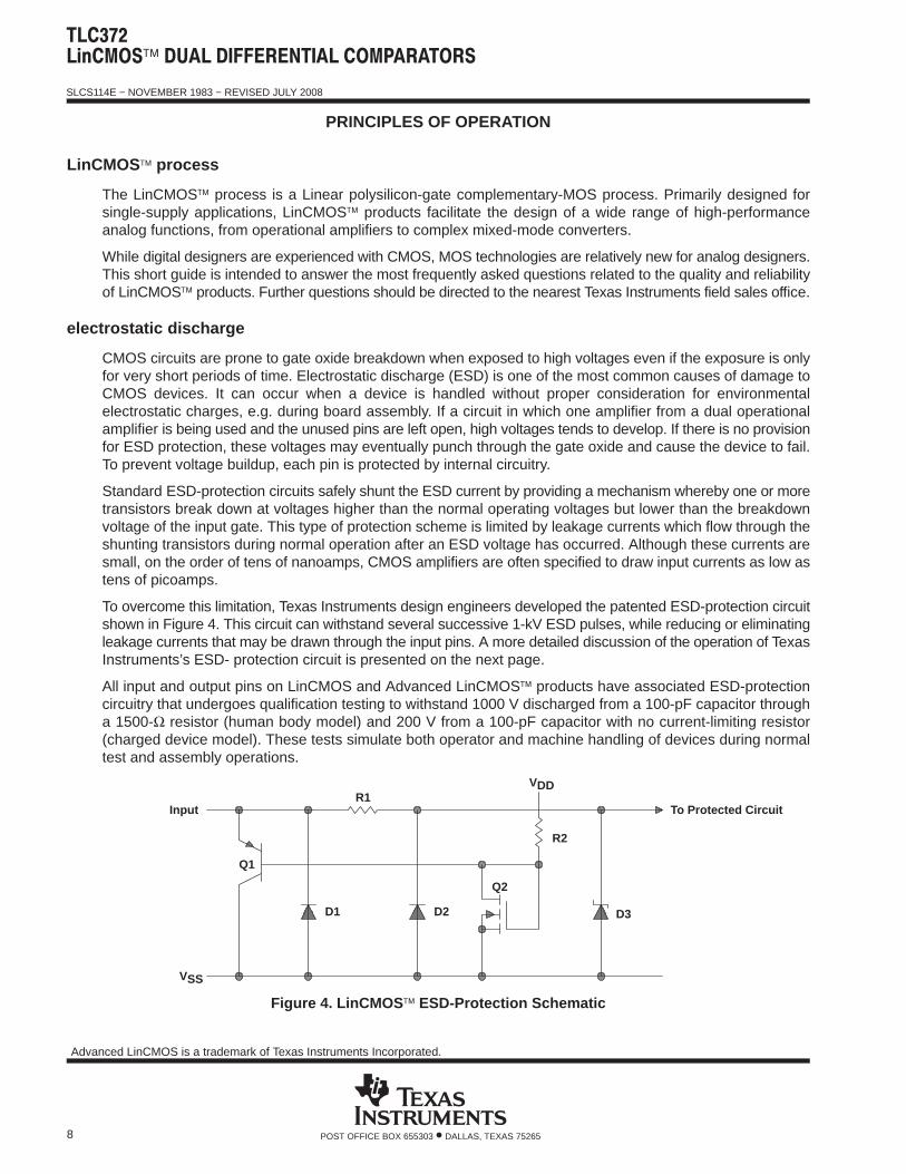
To overcome this limitation, Texas Instruments design engineers developed the patented ESD-protection circuitshown in Figure 4. This circuit can withstand several successive 1-kV ESD pulses, while reducing or eliminatingleakage currents that may be drawn through the input pins. A more detailed discussion of the operation of TexasInstruments’s ESD- protection circuit is presented on the next page.
All input and output pins on LinCMOS and Advanced LinCMOS products have associated ESD-protectioncircuitry that undergoes qualification testing to withstand 1000 V discharged from a 100-pF capacitor througha 1500-Ω resistor (human body model) and 200 V from a 100-pF capacitor with no current-limiting resistor(charged device model). These tests simulate both operator and machine handling of devices during normaltest and assembly operations.
D3
R2
Q2
To Protected Circuit
VDD
D2D1
Q1
R1Input
VSS
Figure 4. LinCMOS ESD-Protection Schematic
Advanced LinCMOS is a trademark of Texas Instruments Incorporated.
SLCS114E − NOVEMBER 1983 − REVISED JULY 2008
9POST OFFICE BOX 655303 • DALLAS, TEXAS 75265
PRINCIPLES OF OPERATION
input protection circuit operation
Texas Instruments’ patented protection circuitry allows for both positive-and negative-going ESD transients.These transients are characterized by extremely fast rise times and usually low energies, and can occur bothwhen the device has all pins open and when it is installed in a circuit.
positive ESD transients
Initial positive charged energy is shunted through Q1 to VSS. Q1 turns on when the voltage at the input risesabove the voltage on the VDD pin by a value equal to the VEB of Q1. The base current increases through R2with input current as Q1 saturates. The base current through R2 forces the voltage at the drain and gate of Q2to exceed its threshold level (VT ~ 22 V to 26 V) and turn Q2 on. The shunted input current through Q1 to VSSis now shunted through the n-channel enhancement-type MOSFET Q2 to VSS. If the voltage on the input pincontinues to rise, the breakdown voltage of the zener diode D3 is exceeded, and all remaining energy isdissipated in R1 and D3. The breakdown voltage of D3 is designed to be 24 V to 27 V, which is well below thegate oxide voltage of the circuit to be protected.
negative ESD transients
The negative charged ESD transients are shunted directly through D1. Additional energy is dissipated in R1and D2 as D2 becomes forward biased. The voltage seen by the protected circuit is −0.3 V to −1 V (the forwardvoltage of D1 and D2).
circuit-design considerations
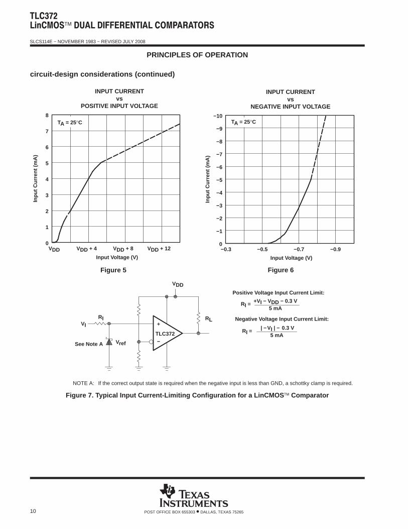
LinCMOS products are being used in actual circuit environments that have input voltages that exceed therecommended common-mode input voltage range and activate the input protection circuit. Even under normaloperation, these conditions occur during circuit power up or power down, and in many cases, when the deviceis being used for a signal conditioning function. The input voltages can exceed VICR and not damage the deviceonly if the inputs are current limited. The recommended current limit shown on most product data sheets is±5 mA. Figure 5 and Figure 6 show typical characteristics for input voltage versus input current.
Normal operation and correct output state can be expected even when the input voltage exceeds the positivesupply voltage. Again, the input current should be externally limited even though internal positive current limitingis achieved in the input protection circuit by the action of Q1. When Q1 is on, it saturates and limits the currentto approximately 5-mA collector current by design. When saturated, Q1 base current increases with inputcurrent. This base current is forced into the VDD pin and into the device IDD or the VDD supply through R2producing the current limiting effects shown in Figure 5. This internal limiting lasts only as long as the inputvoltage is below the VT of Q2.
When the input voltage exceeds the negative supply voltage, normal operation is affected and output voltagestates may not be correct. Also, the isolation between channels of multiple devices (duals and quads) can beseverely affected. External current limiting must be used since this current is directly shunted by D1 and D2 andno internal limiting is achieved. If normal output voltage states are required, an external input voltage clamp isrequired (see Figure 7).
SLCS114E − NOVEMBER 1983 − REVISED JULY 2008
10 POST OFFICE BOX 655303 • DALLAS, TEXAS 75265
PRINCIPLES OF OPERATION
circuit-design considerations (continued)
Figure 5
VDD0
Inpu
t Cur
rent
(m
A)
Input Voltage (V)
8
1
2
3
4
5
6
7
VDD + 4 VDD + 8 VDD + 12
TA = 25°C
INPUT CURRENTvs
POSITIVE INPUT VOLTAGE
Figure 6
TA = 25°C
−0.9−0.7−0.5
Input Voltage (V)
0−0.3
−1
−2
−3
−4
−5
−6
−7
−8
−9
−10
INPUT CURRENTvs
NEGATIVE INPUT VOLTAGE
Inpu
t Cur
rent
(m
A)
−
+
Vref
TLC372
RL
VDD
RI
See Note A
VI
Positive Voltage Input Current Limit:
Negative Voltage Input Current Limit:
RI =+VI − VDD − 0.3 V
5 mA
RI =| −VI | − 0.3 V
5 mA
NOTE A: If the correct output state is required when the negative input is less than GND, a schottky clamp is required.
Figure 7. Typical Input Current-Limiting Configuration for a LinCMOS Comparator
PACKAGE OPTION ADDENDUM
www.ti.com 17-Mar-2017
Addendum-Page 1
PACKAGING INFORMATION
Orderable Device Status(1)
Package Type PackageDrawing
Pins PackageQty
Eco Plan(2)
Lead/Ball Finish(6)
MSL Peak Temp(3)
Op Temp (°C) Device Marking(4/5)
Samples
5962-87658012A ACTIVE LCCC FK 20 1 TBD POST-PLATE N / A for Pkg Type -55 to 125 5962-87658012ATLC372MFKB
5962-8765801PA ACTIVE CDIP JG 8 1 TBD A42 N / A for Pkg Type -55 to 125 8765801PATLC372M
5962-9554901NXD ACTIVE SOIC D 8 2500 Green (RoHS& no Sb/Br)
CU NIPDAU Level-1-260C-UNLIM -55 to 125 Q372M
5962-9554901NXDR ACTIVE SOIC D 8 2500 Green (RoHS& no Sb/Br)
CU NIPDAU Level-1-260C-UNLIM -55 to 125 Q372M
TLC372CD ACTIVE SOIC D 8 75 Green (RoHS& no Sb/Br)
CU NIPDAU Level-1-260C-UNLIM 0 to 70 372C
TLC372CDG4 ACTIVE SOIC D 8 75 Green (RoHS& no Sb/Br)
CU NIPDAU Level-1-260C-UNLIM 0 to 70 372C
TLC372CDR ACTIVE SOIC D 8 2500 Green (RoHS& no Sb/Br)
CU NIPDAU Level-1-260C-UNLIM 0 to 70 372C
TLC372CDRG4 ACTIVE SOIC D 8 2500 Green (RoHS& no Sb/Br)
CU NIPDAU Level-1-260C-UNLIM 0 to 70 372C
TLC372CP ACTIVE PDIP P 8 50 Pb-Free(RoHS)
CU NIPDAU N / A for Pkg Type 0 to 70 TLC372CP
TLC372CPSR ACTIVE SO PS 8 2000 Green (RoHS& no Sb/Br)
CU NIPDAU Level-1-260C-UNLIM 0 to 70 P372
TLC372CPSRG4 ACTIVE SO PS 8 2000 Green (RoHS& no Sb/Br)
CU NIPDAU Level-1-260C-UNLIM 0 to 70 P372
TLC372CPW ACTIVE TSSOP PW 8 150 Green (RoHS& no Sb/Br)
CU NIPDAU Level-1-260C-UNLIM 0 to 70 P372
TLC372CPWG4 ACTIVE TSSOP PW 8 150 Green (RoHS& no Sb/Br)
CU NIPDAU Level-1-260C-UNLIM 0 to 70 P372
TLC372CPWR ACTIVE TSSOP PW 8 2000 Green (RoHS& no Sb/Br)
CU NIPDAU Level-1-260C-UNLIM 0 to 70 P372
TLC372CPWRG4 ACTIVE TSSOP PW 8 2000 Green (RoHS& no Sb/Br)
CU NIPDAU Level-1-260C-UNLIM 0 to 70 P372
TLC372ID ACTIVE SOIC D 8 75 Green (RoHS& no Sb/Br)
(1) The marketing status values are defined as follows:ACTIVE: Product device recommended for new designs.LIFEBUY: TI has announced that the device will be discontinued, and a lifetime-buy period is in effect.NRND: Not recommended for new designs. Device is in production to support existing customers, but TI does not recommend using this part in a new design.PREVIEW: Device has been announced but is not in production. Samples may or may not be available.OBSOLETE: TI has discontinued the production of the device.
(2) Eco Plan - The planned eco-friendly classification: Pb-Free (RoHS), Pb-Free (RoHS Exempt), or Green (RoHS & no Sb/Br) - please check http://www.ti.com/productcontent for the latest availabilityinformation and additional product content details.TBD: The Pb-Free/Green conversion plan has not been defined.Pb-Free (RoHS): TI's terms "Lead-Free" or "Pb-Free" mean semiconductor products that are compatible with the current RoHS requirements for all 6 substances, including the requirement thatlead not exceed 0.1% by weight in homogeneous materials. Where designed to be soldered at high temperatures, TI Pb-Free products are suitable for use in specified lead-free processes.Pb-Free (RoHS Exempt): This component has a RoHS exemption for either 1) lead-based flip-chip solder bumps used between the die and package, or 2) lead-based die adhesive used betweenthe die and leadframe. The component is otherwise considered Pb-Free (RoHS compatible) as defined above.Green (RoHS & no Sb/Br): TI defines "Green" to mean Pb-Free (RoHS compatible), and free of Bromine (Br) and Antimony (Sb) based flame retardants (Br or Sb do not exceed 0.1% by weightin homogeneous material)
(3) MSL, Peak Temp. - The Moisture Sensitivity Level rating according to the JEDEC industry standard classifications, and peak solder temperature.
(4) There may be additional marking, which relates to the logo, the lot trace code information, or the environmental category on the device.
(5) Multiple Device Markings will be inside parentheses. Only one Device Marking contained in parentheses and separated by a "~" will appear on a device. If a line is indented then it is a continuationof the previous line and the two combined represent the entire Device Marking for that device.
(6) Lead/Ball Finish - Orderable Devices may have multiple material finish options. Finish options are separated by a vertical ruled line. Lead/Ball Finish values may wrap to two lines if the finishvalue exceeds the maximum column width.
Important Information and Disclaimer:The information provided on this page represents TI's knowledge and belief as of the date that it is provided. TI bases its knowledge and belief on informationprovided by third parties, and makes no representation or warranty as to the accuracy of such information. Efforts are underway to better integrate information from third parties. TI has taken andcontinues to take reasonable steps to provide representative and accurate information but may not have conducted destructive testing or chemical analysis on incoming materials and chemicals.TI and TI suppliers consider certain information to be proprietary, and thus CAS numbers and other limited information may not be available for release.
In no event shall TI's liability arising out of such information exceed the total purchase price of the TI part(s) at issue in this document sold by TI to Customer on an annual basis.
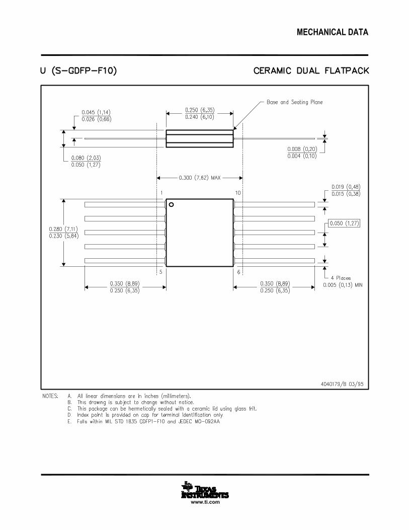
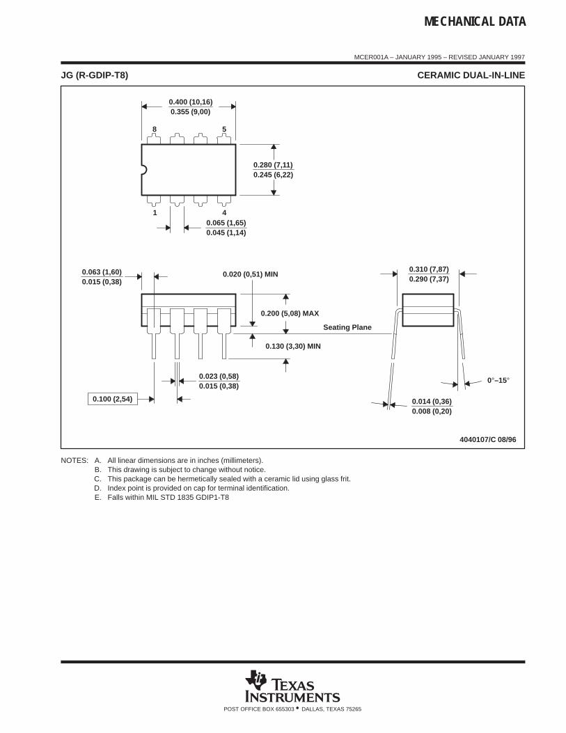
NOTES: A. All linear dimensions are in inches (millimeters).B. This drawing is subject to change without notice.C. This package can be hermetically sealed with a ceramic lid using glass frit.D. Index point is provided on cap for terminal identification.E. Falls within MIL STD 1835 GDIP1-T8
www.ti.com
PACKAGE OUTLINE
C
TYP6.66.2
1.2 MAX
6X 0.65
8X 0.300.19
2X1.95
0.150.05
(0.15) TYP
0 - 8
0.25GAGE PLANE
0.750.50
A
NOTE 3
3.12.9
BNOTE 4
4.54.3
4221848/A 02/2015
TSSOP - 1.2 mm max heightPW0008ASMALL OUTLINE PACKAGE
NOTES: 1. All linear dimensions are in millimeters. Any dimensions in parenthesis are for reference only. Dimensioning and tolerancing per ASME Y14.5M. 2. This drawing is subject to change without notice. 3. This dimension does not include mold flash, protrusions, or gate burrs. Mold flash, protrusions, or gate burrs shall not exceed 0.15 mm per side. 4. This dimension does not include interlead flash. Interlead flash shall not exceed 0.25 mm per side.5. Reference JEDEC registration MO-153, variation AA.
18
0.1 C A B
54
PIN 1 IDAREA
SEATING PLANE
0.1 C
SEE DETAIL A
DETAIL ATYPICAL
SCALE 2.800
www.ti.com
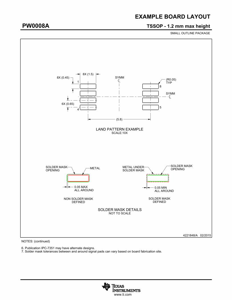
EXAMPLE BOARD LAYOUT
(5.8)
0.05 MAXALL AROUND
0.05 MINALL AROUND
8X (1.5)8X (0.45)
6X (0.65)
(R )TYP
0.05
4221848/A 02/2015
TSSOP - 1.2 mm max heightPW0008ASMALL OUTLINE PACKAGE
SYMM
SYMM
LAND PATTERN EXAMPLESCALE:10X
1
45
8
NOTES: (continued) 6. Publication IPC-7351 may have alternate designs. 7. Solder mask tolerances between and around signal pads can vary based on board fabrication site.
METALSOLDER MASKOPENING
NON SOLDER MASKDEFINED
SOLDER MASK DETAILSNOT TO SCALE
SOLDER MASKOPENING
METAL UNDERSOLDER MASK
SOLDER MASKDEFINED
www.ti.com
EXAMPLE STENCIL DESIGN
(5.8)
6X (0.65)
8X (0.45)8X (1.5)
(R ) TYP0.05
4221848/A 02/2015
TSSOP - 1.2 mm max heightPW0008ASMALL OUTLINE PACKAGE
NOTES: (continued) 8. Laser cutting apertures with trapezoidal walls and rounded corners may offer better paste release. IPC-7525 may have alternate design recommendations. 9. Board assembly site may have different recommendations for stencil design.
SYMM
SYMM
1
45
8
SOLDER PASTE EXAMPLEBASED ON 0.125 mm THICK STENCIL
SCALE:10X
IMPORTANT NOTICE
Texas Instruments Incorporated (TI) reserves the right to make corrections, enhancements, improvements and other changes to itssemiconductor products and services per JESD46, latest issue, and to discontinue any product or service per JESD48, latest issue. Buyersshould obtain the latest relevant information before placing orders and should verify that such information is current and complete.TI’s published terms of sale for semiconductor products (http://www.ti.com/sc/docs/stdterms.htm) apply to the sale of packaged integratedcircuit products that TI has qualified and released to market. Additional terms may apply to the use or sale of other types of TI products andservices.Reproduction of significant portions of TI information in TI data sheets is permissible only if reproduction is without alteration and isaccompanied by all associated warranties, conditions, limitations, and notices. TI is not responsible or liable for such reproduceddocumentation. Information of third parties may be subject to additional restrictions. Resale of TI products or services with statementsdifferent from or beyond the parameters stated by TI for that product or service voids all express and any implied warranties for theassociated TI product or service and is an unfair and deceptive business practice. TI is not responsible or liable for any such statements.Buyers and others who are developing systems that incorporate TI products (collectively, “Designers”) understand and agree that Designersremain responsible for using their independent analysis, evaluation and judgment in designing their applications and that Designers havefull and exclusive responsibility to assure the safety of Designers' applications and compliance of their applications (and of all TI productsused in or for Designers’ applications) with all applicable regulations, laws and other applicable requirements. Designer represents that, withrespect to their applications, Designer has all the necessary expertise to create and implement safeguards that (1) anticipate dangerousconsequences of failures, (2) monitor failures and their consequences, and (3) lessen the likelihood of failures that might cause harm andtake appropriate actions. Designer agrees that prior to using or distributing any applications that include TI products, Designer willthoroughly test such applications and the functionality of such TI products as used in such applications.TI’s provision of technical, application or other design advice, quality characterization, reliability data or other services or information,including, but not limited to, reference designs and materials relating to evaluation modules, (collectively, “TI Resources”) are intended toassist designers who are developing applications that incorporate TI products; by downloading, accessing or using TI Resources in anyway, Designer (individually or, if Designer is acting on behalf of a company, Designer’s company) agrees to use any particular TI Resourcesolely for this purpose and subject to the terms of this Notice.TI’s provision of TI Resources does not expand or otherwise alter TI’s applicable published warranties or warranty disclaimers for TIproducts, and no additional obligations or liabilities arise from TI providing such TI Resources. TI reserves the right to make corrections,enhancements, improvements and other changes to its TI Resources. TI has not conducted any testing other than that specificallydescribed in the published documentation for a particular TI Resource.Designer is authorized to use, copy and modify any individual TI Resource only in connection with the development of applications thatinclude the TI product(s) identified in such TI Resource. NO OTHER LICENSE, EXPRESS OR IMPLIED, BY ESTOPPEL OR OTHERWISETO ANY OTHER TI INTELLECTUAL PROPERTY RIGHT, AND NO LICENSE TO ANY TECHNOLOGY OR INTELLECTUAL PROPERTYRIGHT OF TI OR ANY THIRD PARTY IS GRANTED HEREIN, including but not limited to any patent right, copyright, mask work right, orother intellectual property right relating to any combination, machine, or process in which TI products or services are used. Informationregarding or referencing third-party products or services does not constitute a license to use such products or services, or a warranty orendorsement thereof. Use of TI Resources may require a license from a third party under the patents or other intellectual property of thethird party, or a license from TI under the patents or other intellectual property of TI.TI RESOURCES ARE PROVIDED “AS IS” AND WITH ALL FAULTS. TI DISCLAIMS ALL OTHER WARRANTIES ORREPRESENTATIONS, EXPRESS OR IMPLIED, REGARDING RESOURCES OR USE THEREOF, INCLUDING BUT NOT LIMITED TOACCURACY OR COMPLETENESS, TITLE, ANY EPIDEMIC FAILURE WARRANTY AND ANY IMPLIED WARRANTIES OFMERCHANTABILITY, FITNESS FOR A PARTICULAR PURPOSE, AND NON-INFRINGEMENT OF ANY THIRD PARTY INTELLECTUALPROPERTY RIGHTS. TI SHALL NOT BE LIABLE FOR AND SHALL NOT DEFEND OR INDEMNIFY DESIGNER AGAINST ANY CLAIM,INCLUDING BUT NOT LIMITED TO ANY INFRINGEMENT CLAIM THAT RELATES TO OR IS BASED ON ANY COMBINATION OFPRODUCTS EVEN IF DESCRIBED IN TI RESOURCES OR OTHERWISE. IN NO EVENT SHALL TI BE LIABLE FOR ANY ACTUAL,DIRECT, SPECIAL, COLLATERAL, INDIRECT, PUNITIVE, INCIDENTAL, CONSEQUENTIAL OR EXEMPLARY DAMAGES INCONNECTION WITH OR ARISING OUT OF TI RESOURCES OR USE THEREOF, AND REGARDLESS OF WHETHER TI HAS BEENADVISED OF THE POSSIBILITY OF SUCH DAMAGES.Unless TI has explicitly designated an individual product as meeting the requirements of a particular industry standard (e.g., ISO/TS 16949and ISO 26262), TI is not responsible for any failure to meet such industry standard requirements.Where TI specifically promotes products as facilitating functional safety or as compliant with industry functional safety standards, suchproducts are intended to help enable customers to design and create their own applications that meet applicable functional safety standardsand requirements. Using products in an application does not by itself establish any safety features in the application. Designers mustensure compliance with safety-related requirements and standards applicable to their applications. Designer may not use any TI products inlife-critical medical equipment unless authorized officers of the parties have executed a special contract specifically governing such use.Life-critical medical equipment is medical equipment where failure of such equipment would cause serious bodily injury or death (e.g., lifesupport, pacemakers, defibrillators, heart pumps, neurostimulators, and implantables). Such equipment includes, without limitation, allmedical devices identified by the U.S. Food and Drug Administration as Class III devices and equivalent classifications outside the U.S.TI may expressly designate certain products as completing a particular qualification (e.g., Q100, Military Grade, or Enhanced Product).Designers agree that it has the necessary expertise to select the product with the appropriate qualification designation for their applicationsand that proper product selection is at Designers’ own risk. Designers are solely responsible for compliance with all legal and regulatoryrequirements in connection with such selection.Designer will fully indemnify TI and its representatives against any damages, costs, losses, and/or liabilities arising out of Designer’s non-compliance with the terms and provisions of this Notice.


![CC1310 Integrated Passive Component for 779-928 MHz …8.6 8.7 8.8 8.9 9 9.1 9.2 9.3 x 10 8-60-55-50-45-40-35-30 Frequency [Hz] 5th harmonic [dBm] Min Typ Cond Avg Typ Cond Max Typ](https://static.documents.pub/doc/80x56/60fefb0cc8f3965e93560e26/cc1310-integrated-passive-component-for-779-928-mhz-86-87-88-89-9-91-92-93.jpg)


