35
Automotive Power Data Sheet Rev.1.3.1, 2011-06-27 TLE 6270 R Quad Low Side Injector Driver TLE6270R
Automot ive Power
Data Sheet Rev.1.3.1, 2011-06-27
TLE 6270 RQuad Low Side Injector Driver
TLE6270R
TLE 6270 RQuad Low Side Injector Driver
Table of Contents
Table of Contents
1 Overview . . . . . . . . . . . . . . . . . . . . . . . . . . . . . . . . . . . . . . . . . . . . . . . . . . . . . . . . . . . . . . . . . . . . . . . 4Features . . . . . . . . . . . . . . . . . . . . . . . . . . . . . . . . . . . . . . . . . . . . . . . . . . . . . . . . . . . . . . . . . . . . 4Application . . . . . . . . . . . . . . . . . . . . . . . . . . . . . . . . . . . . . . . . . . . . . . . . . . . . . . . . . . . . . . . . . . . 4General Description . . . . . . . . . . . . . . . . . . . . . . . . . . . . . . . . . . . . . . . . . . . . . . . . . . . . . . . . . . . . 4
2 Block Diagram . . . . . . . . . . . . . . . . . . . . . . . . . . . . . . . . . . . . . . . . . . . . . . . . . . . . . . . . . . . . . . . . . . . 6
3 Pin Configuration . . . . . . . . . . . . . . . . . . . . . . . . . . . . . . . . . . . . . . . . . . . . . . . . . . . . . . . . . . . . . . . . 73.1 Pin Assignment . . . . . . . . . . . . . . . . . . . . . . . . . . . . . . . . . . . . . . . . . . . . . . . . . . . . . . . . . . . . . . . . . . . 73.2 Pin Definitions and Functions . . . . . . . . . . . . . . . . . . . . . . . . . . . . . . . . . . . . . . . . . . . . . . . . . . . . . . . . 8
4 General Product Characteristics . . . . . . . . . . . . . . . . . . . . . . . . . . . . . . . . . . . . . . . . . . . . . . . . . . . . 94.1 Absolute Maximum Ratings . . . . . . . . . . . . . . . . . . . . . . . . . . . . . . . . . . . . . . . . . . . . . . . . . . . . . . . . . 94.2 Functional Range . . . . . . . . . . . . . . . . . . . . . . . . . . . . . . . . . . . . . . . . . . . . . . . . . . . . . . . . . . . . . . . . 104.3 Thermal Resistance . . . . . . . . . . . . . . . . . . . . . . . . . . . . . . . . . . . . . . . . . . . . . . . . . . . . . . . . . . . . . . 10
5 Functional Description . . . . . . . . . . . . . . . . . . . . . . . . . . . . . . . . . . . . . . . . . . . . . . . . . . . . . . . . . . . 115.1 List of Functionalities . . . . . . . . . . . . . . . . . . . . . . . . . . . . . . . . . . . . . . . . . . . . . . . . . . . . . . . . . . . . . 115.2 Load Control . . . . . . . . . . . . . . . . . . . . . . . . . . . . . . . . . . . . . . . . . . . . . . . . . . . . . . . . . . . . . . . . . . . . 115.3 Output Current Control . . . . . . . . . . . . . . . . . . . . . . . . . . . . . . . . . . . . . . . . . . . . . . . . . . . . . . . . . . . . 12
Current Control Configurations according to NON and Pch Signals . . . . . . . . . . . . . . . . . . . . . . 135.4 Diagnostic . . . . . . . . . . . . . . . . . . . . . . . . . . . . . . . . . . . . . . . . . . . . . . . . . . . . . . . . . . . . . . . . . . . . . . 145.4.1 Failures Detection . . . . . . . . . . . . . . . . . . . . . . . . . . . . . . . . . . . . . . . . . . . . . . . . . . . . . . . . . . . . . . 15
OFF State open load Functionality . . . . . . . . . . . . . . . . . . . . . . . . . . . . . . . . . . . . . . . . . . . . . . . 16OFF State Overvoltage Functionality: . . . . . . . . . . . . . . . . . . . . . . . . . . . . . . . . . . . . . . . . . . . . . 16HS Diag Filter Functionality: . . . . . . . . . . . . . . . . . . . . . . . . . . . . . . . . . . . . . . . . . . . . . . . . . . . . 16Diagnostic Control Circuit Functionality: . . . . . . . . . . . . . . . . . . . . . . . . . . . . . . . . . . . . . . . . . . . 16SCn/OLn Definition Circuit Table: . . . . . . . . . . . . . . . . . . . . . . . . . . . . . . . . . . . . . . . . . . . . . . . . 17
5.4.2 Failures Information (via SPI) . . . . . . . . . . . . . . . . . . . . . . . . . . . . . . . . . . . . . . . . . . . . . . . . . . . . . 17Failure Register . . . . . . . . . . . . . . . . . . . . . . . . . . . . . . . . . . . . . . . . . . . . . . . . . . . . . . . . . . . . . . 17Output Coder . . . . . . . . . . . . . . . . . . . . . . . . . . . . . . . . . . . . . . . . . . . . . . . . . . . . . . . . . . . . . . . . 17Input Coder . . . . . . . . . . . . . . . . . . . . . . . . . . . . . . . . . . . . . . . . . . . . . . . . . . . . . . . . . . . . . . . . . 18Shift Register . . . . . . . . . . . . . . . . . . . . . . . . . . . . . . . . . . . . . . . . . . . . . . . . . . . . . . . . . . . . . . . . 19SPI Control . . . . . . . . . . . . . . . . . . . . . . . . . . . . . . . . . . . . . . . . . . . . . . . . . . . . . . . . . . . . . . . . . 19SDO Driver . . . . . . . . . . . . . . . . . . . . . . . . . . . . . . . . . . . . . . . . . . . . . . . . . . . . . . . . . . . . . . . . . 20
5.5 Protections . . . . . . . . . . . . . . . . . . . . . . . . . . . . . . . . . . . . . . . . . . . . . . . . . . . . . . . . . . . . . . . . . . . . . 215.5.1 All Inputs/Outputs . . . . . . . . . . . . . . . . . . . . . . . . . . . . . . . . . . . . . . . . . . . . . . . . . . . . . . . . . . . . . . 215.5.2 T1, T4 Power Transistors . . . . . . . . . . . . . . . . . . . . . . . . . . . . . . . . . . . . . . . . . . . . . . . . . . . . . . . . 215.6 Reset . . . . . . . . . . . . . . . . . . . . . . . . . . . . . . . . . . . . . . . . . . . . . . . . . . . . . . . . . . . . . . . . . . . . . . . . . 21
6 Electrical Characteristics . . . . . . . . . . . . . . . . . . . . . . . . . . . . . . . . . . . . . . . . . . . . . . . . . . . . . . . . . 226.1 Supply Current . . . . . . . . . . . . . . . . . . . . . . . . . . . . . . . . . . . . . . . . . . . . . . . . . . . . . . . . . . . . . . . . . . 226.2 Inputs . . . . . . . . . . . . . . . . . . . . . . . . . . . . . . . . . . . . . . . . . . . . . . . . . . . . . . . . . . . . . . . . . . . . . . . . . 226.3 Outputs . . . . . . . . . . . . . . . . . . . . . . . . . . . . . . . . . . . . . . . . . . . . . . . . . . . . . . . . . . . . . . . . . . . . . . . . 236.4 Current Control . . . . . . . . . . . . . . . . . . . . . . . . . . . . . . . . . . . . . . . . . . . . . . . . . . . . . . . . . . . . . . . . . . 256.5 Current Control Timings . . . . . . . . . . . . . . . . . . . . . . . . . . . . . . . . . . . . . . . . . . . . . . . . . . . . . . . . . . . 266.6 Diagnostic and Protections . . . . . . . . . . . . . . . . . . . . . . . . . . . . . . . . . . . . . . . . . . . . . . . . . . . . . . . . . 266.7 SPI Timings . . . . . . . . . . . . . . . . . . . . . . . . . . . . . . . . . . . . . . . . . . . . . . . . . . . . . . . . . . . . . . . . . . . . 27
7 Diagrams . . . . . . . . . . . . . . . . . . . . . . . . . . . . . . . . . . . . . . . . . . . . . . . . . . . . . . . . . . . . . . . . . . . . . . 297.1 Typical Laws . . . . . . . . . . . . . . . . . . . . . . . . . . . . . . . . . . . . . . . . . . . . . . . . . . . . . . . . . . . . . . . . . . . . 297.2 Output Timings Diagram . . . . . . . . . . . . . . . . . . . . . . . . . . . . . . . . . . . . . . . . . . . . . . . . . . . . . . . . . . . 30
Data Sheet 2 Rev.1.3.1, 2011-06-27

TLE 6270 RQuad Low Side Injector Driver
Table of Contents
8 Application Information . . . . . . . . . . . . . . . . . . . . . . . . . . . . . . . . . . . . . . . . . . . . . . . . . . . . . . . . . . 318.1 Principle Diagram of Injection System . . . . . . . . . . . . . . . . . . . . . . . . . . . . . . . . . . . . . . . . . . . . . . . . 318.2 Typical Waveform Diagrams for One and Two Outputs Control . . . . . . . . . . . . . . . . . . . . . . . . . . . . . 32
9 Package Outlines . . . . . . . . . . . . . . . . . . . . . . . . . . . . . . . . . . . . . . . . . . . . . . . . . . . . . . . . . . . . . . . 33Green Product (RoHS compliant) . . . . . . . . . . . . . . . . . . . . . . . . . . . . . . . . . . . . . . . . . . . . . . . . 33
10 Revision History . . . . . . . . . . . . . . . . . . . . . . . . . . . . . . . . . . . . . . . . . . . . . . . . . . . . . . . . . . . . . . . . 34
Data Sheet 3 Rev.1.3.1, 2011-06-27
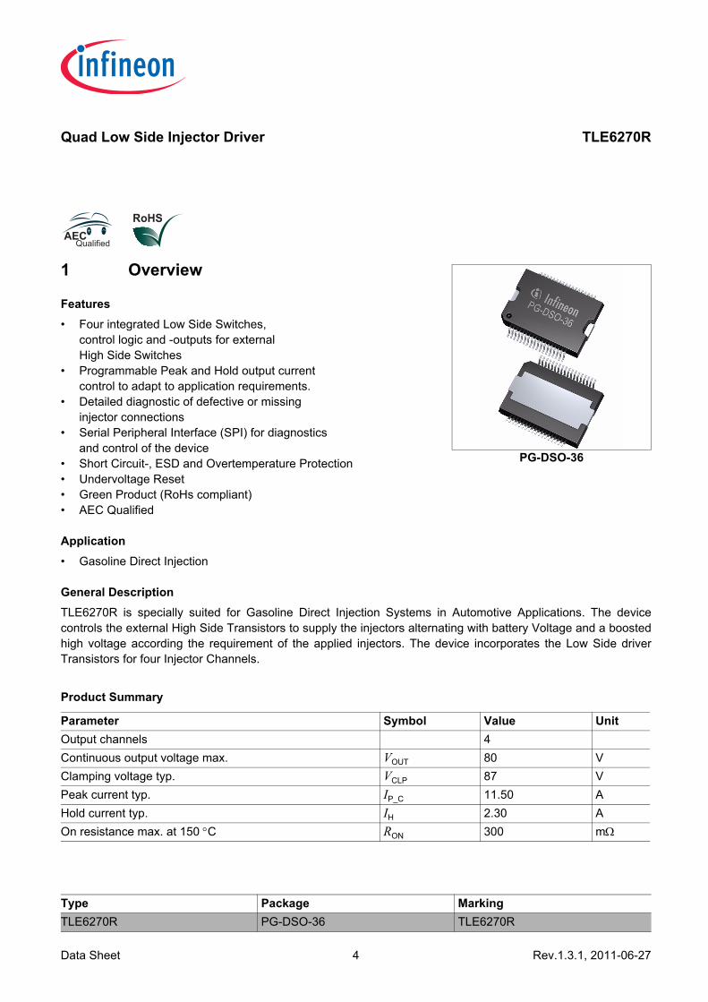
Quad Low Side Injector Driver
TLE6270R
PG-DSO-36
1 Overview
Features• Four integrated Low Side Switches,
control logic and -outputs for external High Side Switches
• Programmable Peak and Hold output current control to adapt to application requirements.
• Detailed diagnostic of defective or missing injector connections
• Serial Peripheral Interface (SPI) for diagnostics and control of the device
• Short Circuit-, ESD and Overtemperature Protection• Undervoltage Reset• Green Product (RoHs compliant)• AEC Qualified
Application• Gasoline Direct Injection
General DescriptionTLE6270R is specially suited for Gasoline Direct Injection Systems in Automotive Applications. The devicecontrols the external High Side Transistors to supply the injectors alternating with battery Voltage and a boostedhigh voltage according the requirement of the applied injectors. The device incorporates the Low Side driverTransistors for four Injector Channels.
Product Summary
Parameter Symbol Value UnitOutput channels 4Continuous output voltage max. VOUT 80 VClamping voltage typ. VCLP 87 VPeak current typ. IP_C 11.50 AHold current typ. IH 2.30 AOn resistance max. at 150 °C RON 300 mΩ
Type Package MarkingTLE6270R PG-DSO-36 TLE6270R
Data Sheet 4 Rev.1.3.1, 2011-06-27
TLE 6270 RQuad Low Side Injector Driver
Overview
Figure 1 Application Diagram
Micro controller
TLE 6270 R
5 KΩ
Loads5V
HS diagnosis circuitry
Bank A Bank B
HS diagnosis circuitry
5 KΩ
Loads
Batt80V
SPI
Inputs
Reset
Programming resistors
External oscillator
Data Sheet 5 Rev.1.3.1, 2011-06-27
Data Sheet 6 Rev.1.3.1, 2011-06-27
TLE 6270 RQuad Low Side Injector Driver
Block Diagram
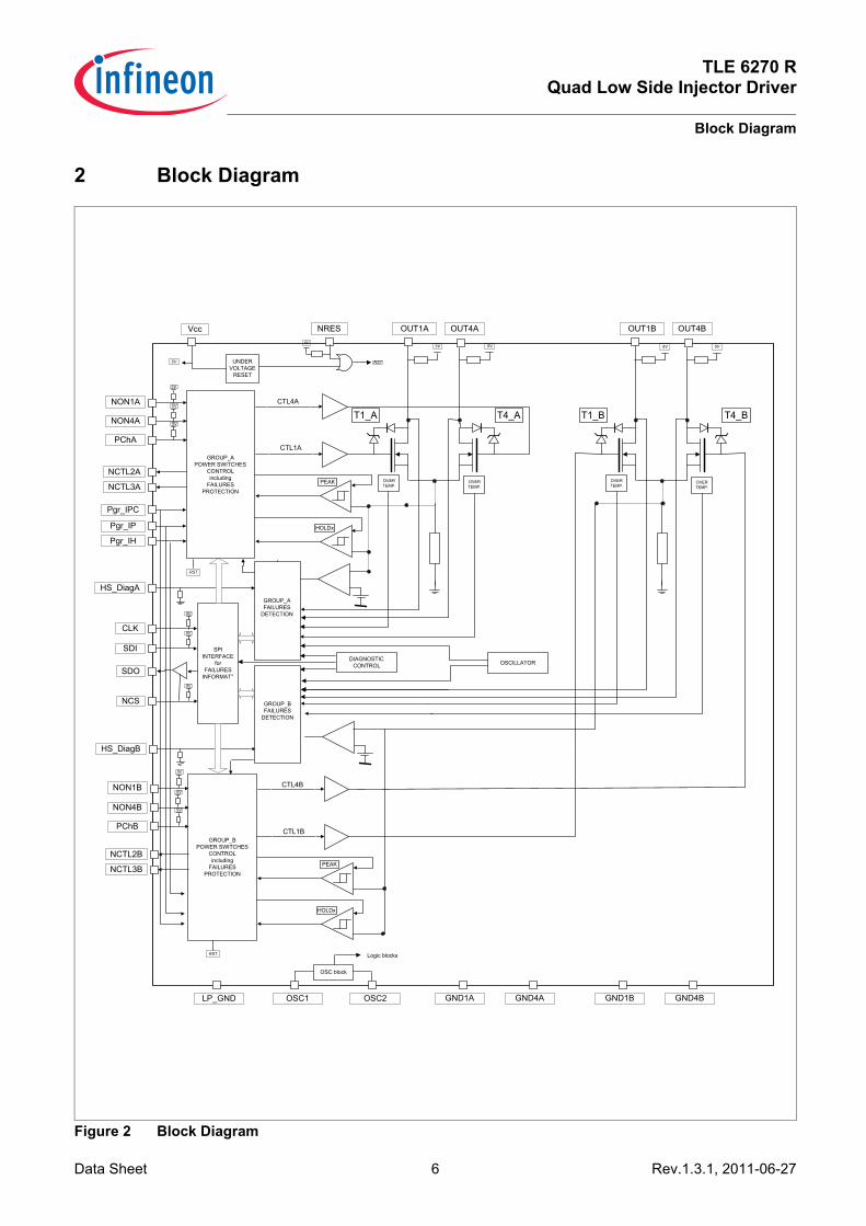
2 Block Diagram
Figure 2 Block Diagram
GROUP_APOWER SWITCHES
CONTROLincluding
FAILURESPROTECTION
GROUP_AFAILURES
DETECTION
PEAK
HOLDx
NON1A
NON4A
PChA
NCTL2A
NCTL3A
Pgr_IP
Pgr_IH
HS_DiagA
CLK
SDI
SDO
NCS
SPIINTERFACE
forFAILURES
INFORMAT°
NRES OUT1A OUT4AVcc
UNDERVOLTAGE
RESET
RST5V
LP_GND
RST
T1_A T4_A
Pgr_IPC
GROUP_BPOWER SWITCHES
CONTROLincluding
FAILURESPROTECTION
PEAK
HOLDx
NON1B
NON4B
PChB
NCTL2B
NCTL3B
HS_DiagB
RST
OVERTEMP.
OVERTEMP.
OUT1B OUT4B
T1_B T4_B
OVERTEMP.
OVERTEMP.
GROUP_BFAILURES
DETECTION
GND1A GND4A GND1B GND4B
5V5V5V5V
DIAGNOSTICCONTROL OSCILLATOR
5V
5V
5V
5V
5V
5V
5V
5V
5V
5V
CTL4A
CTL1A
CTL4B
CTL1B
OSC block
OSC1
Logic blocks
OSC2
TLE 6270 RQuad Low Side Injector Driver
Pin Configuration
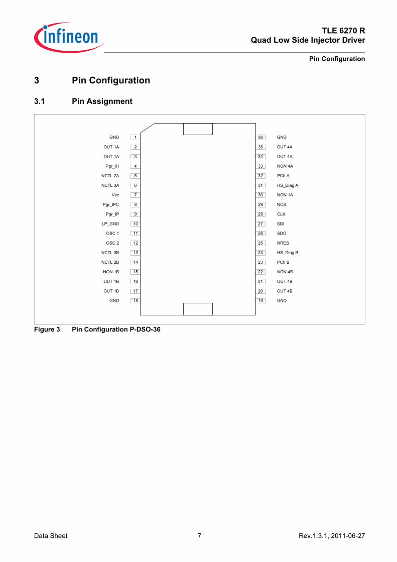
3 Pin Configuration
3.1 Pin Assignment
Figure 3 Pin Configuration P-DSO-36
Vcc
LP_GND
Pgr_IP
Pgr_IPC
Pgr_IH
OSC 2
OSC 1
NON 1B
NCTL 2A
NCTL 3A
OUT 1B
NCTL 2B
NCTL 3B
OUT 1A
GND
GND
OUT 1A
OUT 1B
1
2
3
4
5
6
7
8
9
10
11
12
13
14
15
16
17
18
NON 4A
NON 1A
PCh A
NRES
NON 4B
PCh B
CLK
NCS
SDI
SDO
OUT 4B
OUT 4A
HS_Diag A
HS_Diag B
GND
GND
OUT 4A
OUT 4B
19
20
21
22
23
24
25
26
27
28
29
30
31
32
33
36
35
34
Data Sheet 7 Rev.1.3.1, 2011-06-27
TLE 6270 RQuad Low Side Injector Driver
Pin Configuration
3.2 Pin Definitions and Functions
Pin Symbol Function7 VCC 5 V Power Supply10 LPGND Low Power Ground1 GND High Power Ground18 GND High Power Ground19 GND High Power Ground36 GND High Power Ground2 OUT1A OUTPUT channel 1A3 OUT1A OUTPUT channel 1A34 OUT4A OUTPUT channel 4A35 OUT4A OUTPUT channel 4A16 OUT1B OUTPUT channel 1B17 OUT1B OUTPUT channel 1B20 OUT4B OUTPUT channel 4B21 OUT4B OUTPUT channel 4B30 NON1A Control input channel 1A33 NON4A Control input channel 4A15 NON1B Control input channel 1B22 NON4B Control input channel 4B32 PChA Pre-charge input group A23 PChB Pre-charge input group B8 Pgr_IPC IPC programming input1)
1) If there is no pre-charge resistor this pin has to be connected to VCC on the PCB
9 Pgr_IP IP programming input4 Pgr_IH IH programming input5 NCTL2A Control output high side 2A6 NCTL3A Control output high side 3A14 NCTL2B Control output high side 2B13 NCTL3B Control output high side 3B31 HS_Diag A High side diagnostic input A24 HS_Diag B High side diagnostic input B25 NRES Reset input27 SDI Serial Data Input26 SDO Serial Data Output28 CLK Clock input for serial interface29 NCS Chip-select input11 OSC1 External resonator input12 OSC2 External resonator output– Case Note: Has to be connected to GND on the PCB
Data Sheet 8 Rev.1.3.1, 2011-06-27
TLE 6270 RQuad Low Side Injector Driver
General Product Characteristics
4 General Product Characteristics
4.1 Absolute Maximum Ratings
Note: Stresses above the ones listed here may cause permanent damage to the device. Exposure to absolute maximum rating conditions for extended periods may affect device reliability.
Note: Integrated protection functions are designed to prevent IC destruction under fault conditions described in the data sheet. Fault conditions are considered as “outside” normal operating range. Protection functions are not designed for continuous repetitive operation.
Figure 4 Energy Repetitive Pulse and Energy Single Pulse
Absolute Maximum Ratings 1)
TJ = -40 °C to +150 °C; all voltages with respect to ground, positive current flowing into pin(unless otherwise specified)
1) Not subject to production test, specified by design.
Pos. Parameter Symbol Limit Values Unit ConditionsMin. Max.
4.1.1 Supply voltage VCC -0.3 7 V –Outputs4.1.2 Continuous output voltage VOUT -1.5 80 V –4.1.3 Continuous output current, one output
activeIOUTC -5 5 A –
4.1.4 Peak output current IOUTP -10 20 A see Chapter 5.54.1.5 Clamping energy repetitive pulse WOFFr – 30 mJ all T°, see Figure 44.1.6 Clamping energy single pulse WOFFs – 130 mJ all T°, see Figure 4Inputs and NCTL, SDO outputs4.1.7 Continuous voltage VIN -0.3 7 V –All pinsESD Susceptibility4.1.8 Electrostatic discharge VESD -2000 2000 V R = 1.5 kΩ;
C = 100 pF;HBM2)
2) ESD susceptibility, HBM according to EIA/JESD 22-A114B
Operating Range4.1.9 Operating Temperature Range TJ -40 150 °C 1)
4.1.10 Storage Temperature Range TJ -55 150 °C 1)
250 us
100ns
10%
90% 240 W
P
t
f=1 kHz
500 us
100ns
10%
90%520 W
P
t
Data Sheet 9 Rev.1.3.1, 2011-06-27
TLE 6270 RQuad Low Side Injector Driver
General Product Characteristics
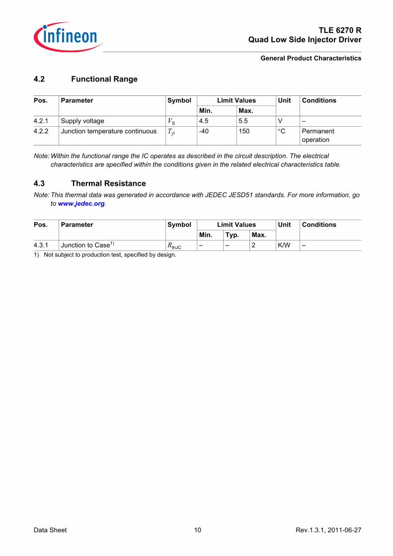
4.2 Functional Range
Note: Within the functional range the IC operates as described in the circuit description. The electrical characteristics are specified within the conditions given in the related electrical characteristics table.
4.3 Thermal ResistanceNote: This thermal data was generated in accordance with JEDEC JESD51 standards. For more information, go
to www.jedec.org.
Pos. Parameter Symbol Limit Values Unit ConditionsMin. Max.
4.2.1 Supply voltage VS 4.5 5.5 V –4.2.2 Junction temperature continuous Tj1 -40 150 °C Permanent
operation
Pos. Parameter Symbol Limit Values Unit ConditionsMin. Typ. Max.
4.3.1 Junction to Case1)
1) Not subject to production test, specified by design.RthJC – – 2 K/W –
Data Sheet 10 Rev.1.3.1, 2011-06-27

TLE 6270 RQuad Low Side Injector Driver
Functional Description
5 Functional Description
5.1 List of FunctionalitiesThe device performs the following functionalities:• Load control
– 4 low side power transistors driven by 4 parallel CMOS compatible inputs.• Output current control
– output current comparators and logic circuit to generate high side switches control signals NCTL2 and NCTL3.
– current thresholds programmable by external resistor.• Diagnostic of defective or missing injector connections and overtemperature
– comparators and logic circuit to interpret unexpected current, voltages and HSDiag input status as short circuit or disconnection of the injector.
– 4 thermal sensors for independent overtemperature detection on the 4 channels.• Protection
– all inputs/outputs: protection against ESD (all input and output pins)– T1, T4, internal power transistors: protection against overvoltage and Transients (Schaffner test pulses)…– external transistors connected via NCTL2 and CLT3: protection against overvoltage and Transients
(Schaffner test pulses)…• Reset
– external reset (reset pin)– internal reset (undervoltage reset)
• Electro Magnetic Compatibility (EMC)These functionalities are described in the next chapters.
5.2 Load ControlEach output transistor is switched on and off by an individual control signal (NON input).In normal operation, when NON is low, the transistor is ON and when NON is high the transistor is OFF. Also afterpower up, the outputs must have the status defined by the NON input.The logic level of the input is CMOS compatible.As there is an internal pull-up, the output transistor is switched off when the input is not connected.It is possible to drive two separate loads simultaneously as far as they do not belong to the same bank.
Data Sheet 11 Rev.1.3.1, 2011-06-27
TLE 6270 RQuad Low Side Injector Driver
Functional Description
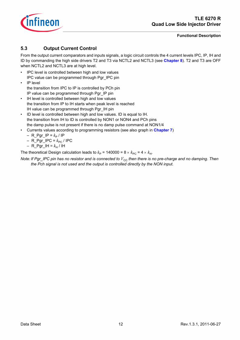
5.3 Output Current ControlFrom the output current comparators and inputs signals, a logic circuit controls the 4 current levels IPC, IP, IH andID by commanding the high side drivers T2 and T3 via NCTL2 and NCTL3 (see Chapter 8). T2 and T3 are OFFwhen NCTL2 and NCTL3 are at high level.• IPC level is controlled between high and low values
IPC value can be programmed through Pgr_IPC pin• IP level
the transition from IPC to IP is controlled by PCh pinIP value can be programmed through Pgr_IP pin
• IH level is controlled between high and low valuesthe transition from IP to IH starts when peak level is reachedIH value can be programmed through Pgr_IH pin
• ID level is controlled between high and low values. ID is equal to IH.the transition from IH to ID is controlled by NON1 or NON4 and PCh pinsthe damp pulse is not present if there is no damp pulse command at NON1/4
• Currents values according to programming resistors (see also graph in Chapter 7)– R_Pgr_IP = kP / IP – R_Pgr_IPC = kPC / IPC– R_Pgr_IH = kH / IH
The theoretical Design calculation leads to kP = 140000 = 8 × kPC = 4 × kH.Note: If Pgr_IPC pin has no resistor and is connected to VCC then there is no pre-charge and no damping. Then
the Pch signal is not used and the output is controlled directly by the NON input.
Data Sheet 12 Rev.1.3.1, 2011-06-27
TLE 6270 RQuad Low Side Injector Driver
Functional Description
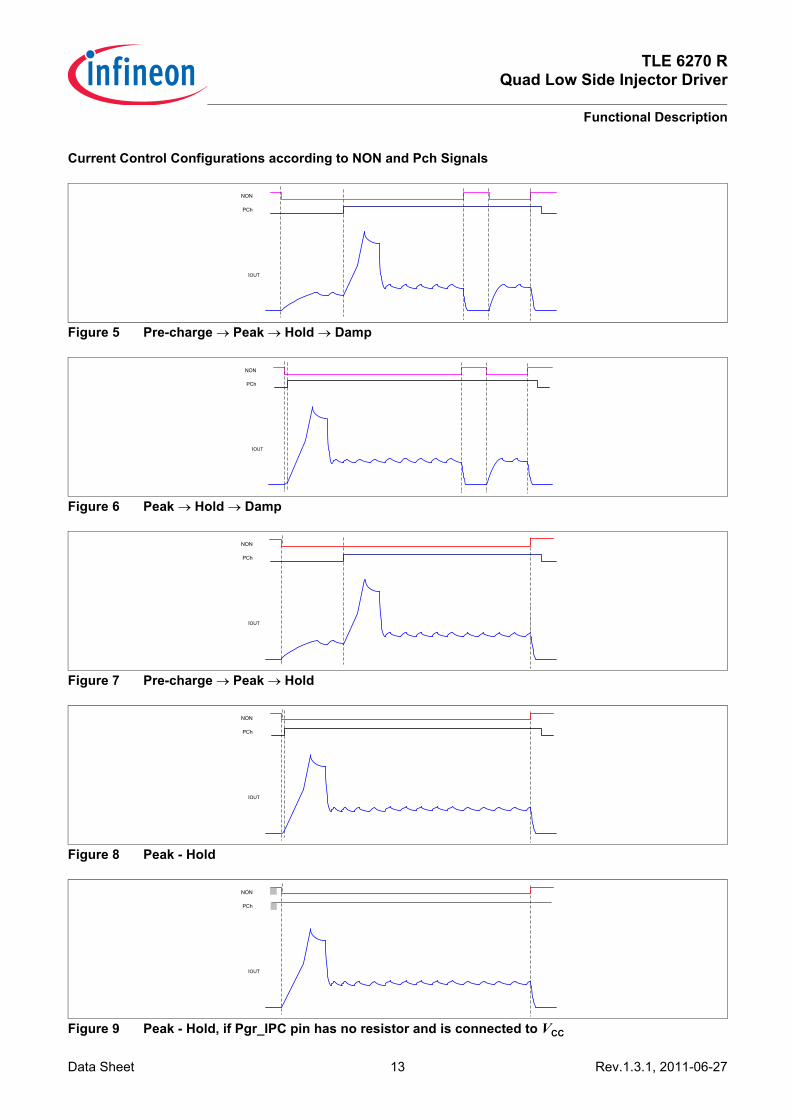
Current Control Configurations according to NON and Pch Signals
Figure 5 Pre-charge → Peak → Hold → Damp
Figure 6 Peak → Hold → Damp
Figure 7 Pre-charge → Peak → Hold
Figure 8 Peak - Hold
Figure 9 Peak - Hold, if Pgr_IPC pin has no resistor and is connected to VCC
NON
PCh
IOUT
NON
PCh
IOUT
NON
PCh
IOUT
NON
PCh
IOUT
NON
PCh
IOUT
Data Sheet 13 Rev.1.3.1, 2011-06-27
TLE 6270 RQuad Low Side Injector Driver
Functional Description
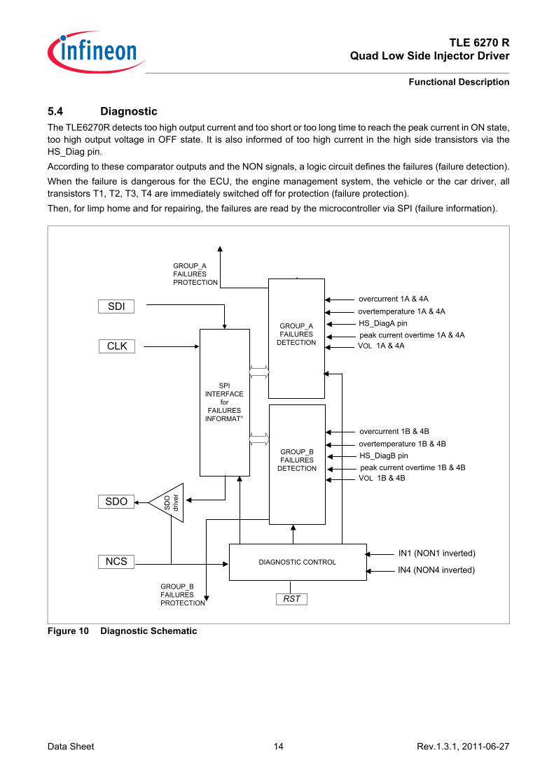
5.4 DiagnosticThe TLE6270R detects too high output current and too short or too long time to reach the peak current in ON state,too high output voltage in OFF state. It is also informed of too high current in the high side transistors via theHS_Diag pin.According to these comparator outputs and the NON signals, a logic circuit defines the failures (failure detection).When the failure is dangerous for the ECU, the engine management system, the vehicle or the car driver, alltransistors T1, T2, T3, T4 are immediately switched off for protection (failure protection).Then, for limp home and for repairing, the failures are read by the microcontroller via SPI (failure information).
Figure 10 Diagnostic Schematic
GROUP_AFAILURES
DETECTIONCLK
SDI
SDO
NCS
SDO
driv
er
SPIINTERFACE
forFAILURES
INFORMAT°
GROUP_BFAILURES
DETECTION
DIAGNOSTIC CONTROL
GROUP_AFAILURESPROTECTION
GROUP_BFAILURESPROTECTION RST
IN1 (NON1 inverted)
IN4 (NON4 inverted)
overcurrent 1A & 4Aovertemperature 1A & 4AHS_DiagA pinpeak current overtime 1A & 4AVOL 1A & 4A
overcurrent 1B & 4Bovertemperature 1B & 4BHS_DiagB pinpeak current overtime 1B & 4BVOL 1B & 4B
Data Sheet 14 Rev.1.3.1, 2011-06-27
TLE 6270 RQuad Low Side Injector Driver
Functional Description
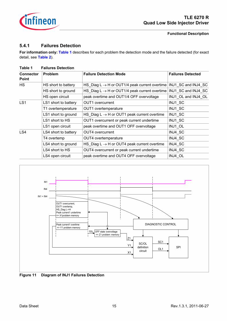
5.4.1 Failures DetectionFor information only: Table 1 describes for each problem the detection mode and the failure detected (for exactdetail, see Table 2).
Figure 11 Diagram of INJ1 Failures Detection
Table 1 Failures DetectionConnector Point
Problem Failure Detection Mode Failures Detected
HS HS short to battery HS_Diag L → H or OUT1/4 peak current overtime INJ1_SC and INJ4_SCHS short to ground HS_Diag L → H or OUT1/4 peak current overtime INJ1_SC and INJ4_SCHS open circuit peak overtime and OUT1/4 OFF overvoltage INJ1_OL and INJ4_OL
LS1 LS1 short to battery OUT1 overcurrent INJ1_SCT1 overtemperature OUT1 overtemperature INJ1_SCLS1 short to ground HS_Diag L → H or OUT1 peak current overtime INJ1_SCLS1 short to HS OUT1 overcurrent or peak current undertime INJ1_SCLS1 open circuit peak overtime and OUT1 OFF overvoltage INJ1_OL
LS4 LS4 short to battery OUT4 overcurrent INJ4_SCT4 overtemp OUT4 overtemperature INJ4_SCLS4 short to ground HS_Diag L → H or OUT4 peak current overtime INJ4_SCLS4 short to HS OUT4 overcurrent or peak current undertime INJ4_SCLS4 open circuit peak overtime and OUT4 OFF overvoltage INJ4_OL
IN1
IN1 + IN4
IN4
OUT1 overcurrent, OUT1 overtemp, HS_Diag L->H Peak current1 undertime => X1problem memory
Peak current1 overtime => Y1 problem memory
tOL OFF state overvoltage => Z1 problem memory
SC/OLdefinition
circuit
SC1
OL1
DIAGNOSTIC CONTROL
SPI
Z1
Y1
X1
Data Sheet 15 Rev.1.3.1, 2011-06-27
TLE 6270 RQuad Low Side Injector Driver
Functional Description
OFF State open load FunctionalityThe TLE6270GR is able to detect a missing load in OFF-state using a pull-up resistor connected at the outputwhen the both outputs of the correspoding bank are turned off.For the correct functionality of this feature a 5KΩ resistor has to be connected in parallel with the freewheelingdiode of each bank.
OFF State Overvoltage Functionality:• Comparator:
– There is one comparator for two channels. A low level on the comparator output (called VOFF) means no failure.
– The voltage on OUT1 (resp. OUT4) is checked at the OFF state between OUT1 and OUT4 ON states (resp. between OUT4 and OUT1 ON states).
• Filter time: For OUT1 (resp. OUT4), the filter time starts:– at H → L transition on IN1 (resp. IN4)– if VOFF is high when this first filter time is finished– at every L → H transition on VOFF
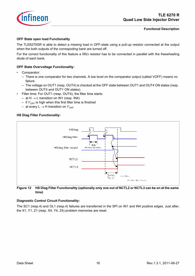
HS Diag Filter Functionality:
Figure 12 HS Diag Filter Functionality (optionally only one out of NCTL2 or NCTL3 can be on at the same time)
Diagnostic Control Circuit Functionality:The SC1 (resp.4) and OL1 (resp.4) failures are transferred in the SPI on IN1 and IN4 positive edges. Just after,the X1, Y1, Z1 (resp. X4, Y4, Z4) problem memories are reset.
Min. 50ns, max.250ns
Data Sheet 16 Rev.1.3.1, 2011-06-27

TLE 6270 RQuad Low Side Injector Driver
Functional Description
SCn/OLn Definition Circuit Table:
5.4.2 Failures Information (via SPI)The failures detected are communicated to the microcontroller via a Serial/Peripheral Interface (SPI) in order tominimize the pin number.The SPI contains a failure register, a coder, a shift register, and a SDO driver:
Figure 13 Failures Information
Failure RegisterEach failure is stored in an individual register (this cannot be done directly in the shift register because a failurecan occur while the shift register is being read).If the failure occurs, it remains until the SPI is read.The failure register is cleared when the SPI is read (FR_CLEAR signal).
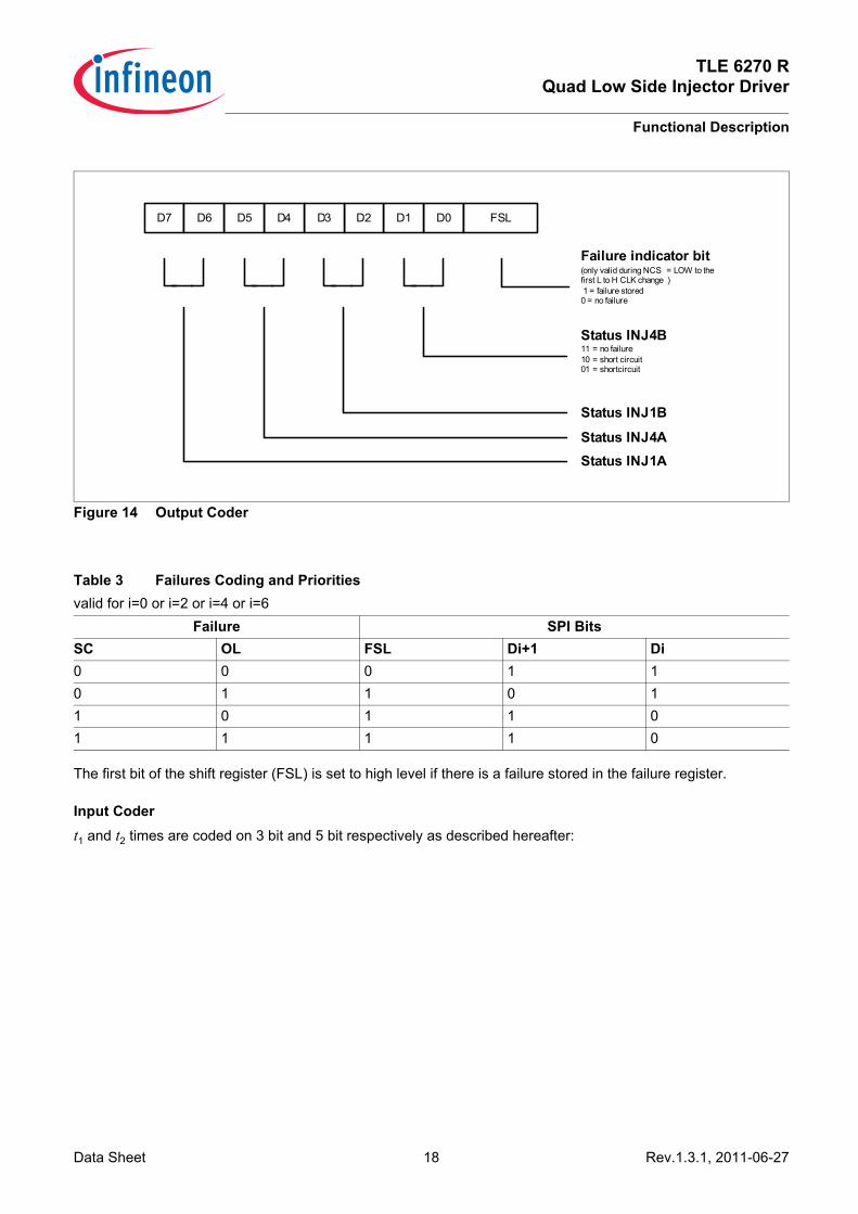
Output CoderThe SC and OL failures of the 4 outputs are coded on an 8 bit word described hereafter:
Table 2 SC/OL Definition Circuitvalid for n=1 or n=4
Memories FailuresXn Yn Zn SCn OLn0 0 0 0 00 0 1 0 00 1 0 1 00 1 1 0 11 0 0 1 01 0 1 1 01 1 0 1 01 1 1 1 0
FAILUREREGISTERCODERSHIFT
REGISTER
CLK
SDI
SDO
NCS
D0
FSL
D3
D2
D1
D4
D5
D7
D6
DIAGNOSTIC_CONTROL
SDODRIVER
INJ1A_OL
INJ1A_SC
INJ4A_OL
INJ4A_SC
INJ4B_OL
INJ4B_SC
INJ1B_OL
INJ1B_SC
INJ1A_OL_stored
INJ1A_SC_stored
INJ4A_OL_stored
INJ4A_SC_stored
INJ4B_OL_stored
INJ4B_SC_stored
INJ1B_OL_stored
INJ1B_SC_stored
Data Sheet 17 Rev.1.3.1, 2011-06-27
TLE 6270 RQuad Low Side Injector Driver
Functional Description
Figure 14 Output Coder
The first bit of the shift register (FSL) is set to high level if there is a failure stored in the failure register.
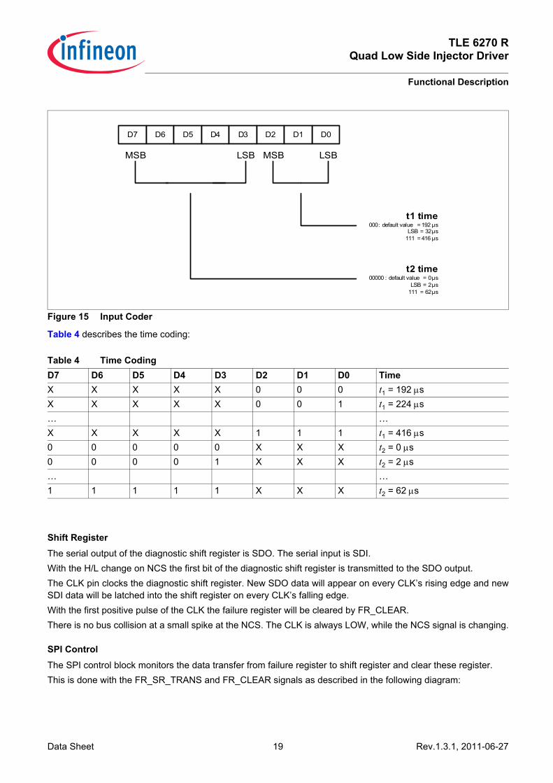
Input Codert1 and t2 times are coded on 3 bit and 5 bit respectively as described hereafter:
Table 3 Failures Coding and Prioritiesvalid for i=0 or i=2 or i=4 or i=6
Failure SPI BitsSC OL FSL Di+1 Di0 0 0 1 10 1 1 0 11 0 1 1 01 1 1 1 0
D7 D0D1D2D3D4D5D6 FSL
Status INJ4B11 = no failure10 = short circuit01 = shortcircuit
Status INJ1B
Failure indicator bit(only valid during NCS = LOW to the first L to H CLK change ) 1 = failure stored0 = no failure
Status INJ4AStatus INJ1A
Data Sheet 18 Rev.1.3.1, 2011-06-27
TLE 6270 RQuad Low Side Injector Driver
Functional Description
Figure 15 Input Coder
Table 4 describes the time coding:
Shift RegisterThe serial output of the diagnostic shift register is SDO. The serial input is SDI.With the H/L change on NCS the first bit of the diagnostic shift register is transmitted to the SDO output.The CLK pin clocks the diagnostic shift register. New SDO data will appear on every CLK’s rising edge and newSDI data will be latched into the shift register on every CLK’s falling edge.With the first positive pulse of the CLK the failure register will be cleared by FR_CLEAR.There is no bus collision at a small spike at the NCS. The CLK is always LOW, while the NCS signal is changing.
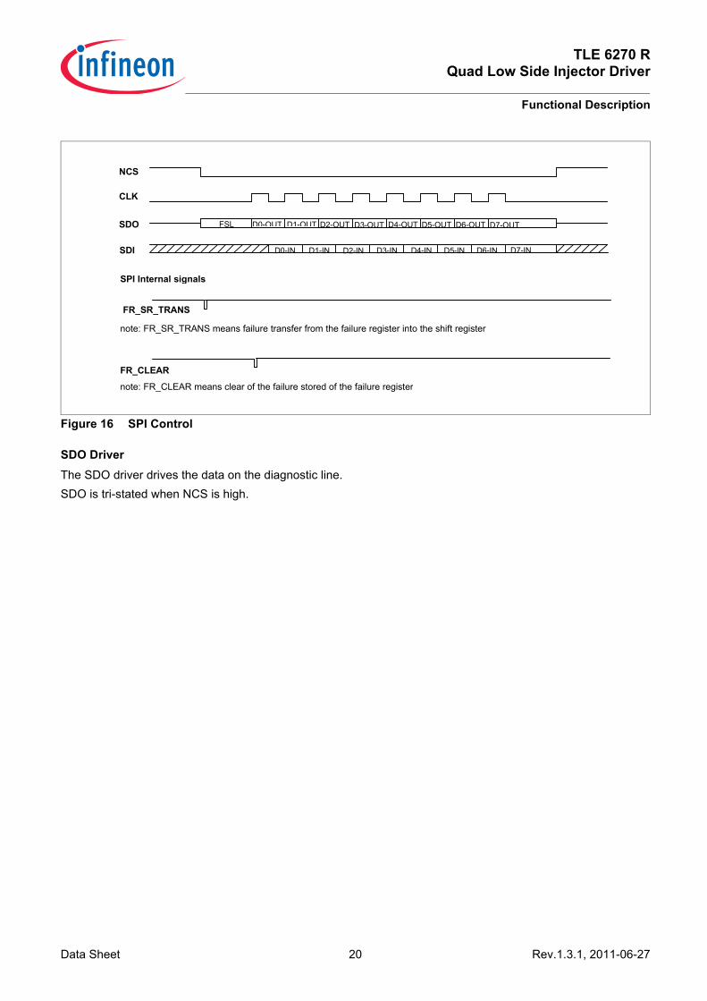
SPI ControlThe SPI control block monitors the data transfer from failure register to shift register and clear these register.This is done with the FR_SR_TRANS and FR_CLEAR signals as described in the following diagram:
Table 4 Time CodingD7 D6 D5 D4 D3 D2 D1 D0 TimeX X X X X 0 0 0 t1 = 192 μsX X X X X 0 0 1 t1 = 224 μs… …X X X X X 1 1 1 t1 = 416 μs0 0 0 0 0 X X X t2 = 0 μs0 0 0 0 1 X X X t2 = 2 μs… …1 1 1 1 1 X X X t2 = 62 μs
D0D7 D6 D5 D4 D3 D2 D1
t1 time000: default value = 192 µs
LSB = 32µs111 = 416 µs
t2 time00000 : default value = 0µs
LSB = 2µs111 = 62µs
LSBMSBMSB LSB
Data Sheet 19 Rev.1.3.1, 2011-06-27
TLE 6270 RQuad Low Side Injector Driver
Functional Description
Figure 16 SPI Control
SDO DriverThe SDO driver drives the data on the diagnostic line.SDO is tri-stated when NCS is high.
CLK
NCS
SDO D0-OUTFSL D1-OUT D2-OUT D3-OUT D6-OUTD5-OUTD4-OUT D7-OUT
D7-IND6-IND5-IND3-IN D4-IND0-IN D1-IN D2-INSDI
FR_SR_TRANS
note: FR_SR_TRANS means failure transfer from the failure register into the shift register
FR_CLEAR
note: FR_CLEAR means clear of the failure stored of the failure register
SPI Internal signals
Data Sheet 20 Rev.1.3.1, 2011-06-27
TLE 6270 RQuad Low Side Injector Driver
Functional Description
5.5 Protections
5.5.1 All Inputs/OutputsAll pins are protected against ESD 2kV Human body model.
5.5.2 T1, T4 Power Transistors• Protection against damaging failures
Note: The protection latches are reset when the NON input is at high level.
• Protection against overvoltageA clamping circuit limits the output voltage to a defined value (Vclp) in order to avoid the breakdown of the output transistor when the solenoid load is switched off.
• Protection against turn on due to fast voltage ramp on output.A very fast voltage slope on the output can turn on the power transistor (capacitive effects) especially when the normal gate pull-down structure is not active (IC not supplied, VCC too low …). In this case, the transistor is turned off immediately. This function is guaranteed for VCC between 0 and 5.5 V.
5.6 ResetThere are two different reset functions:• Undervoltage reset• NRES reset pinIf one or several of the following conditions are present:• VCC lower than VCCRES,• NRES pin at low level,the low side T1, T4 are switched off, NCTL2 and NCTL3 set to high level, all diagnostic registers are reset and theSDO is tri-stated.
Table 5 Protection against Damaging FailuresProblem detected Transistors switched offT1 or T4 overcurrent T1, T4 (internally) and T2, T3 (via NCTL2, NCTL3)T1 or T4 overtemperature T1, T4 (internally) and T2, T3 (via NCTL2, NCTL3)HS_Diag L → H T1, T4 (internally) and T2, T3 (via NCTL2, NCTL3)T1 or T4 peak current undertime T1, T4 (internally) and T2, T3 (via NCTL2, NCTL3)T1 or T4 peak current overtime T1, T4 (internally) and T2, T3 (via NCTL2, NCTL3) and t2 starts.
Data Sheet 21 Rev.1.3.1, 2011-06-27
TLE 6270 RQuad Low Side Injector Driver
Electrical Characteristics
6 Electrical Characteristics
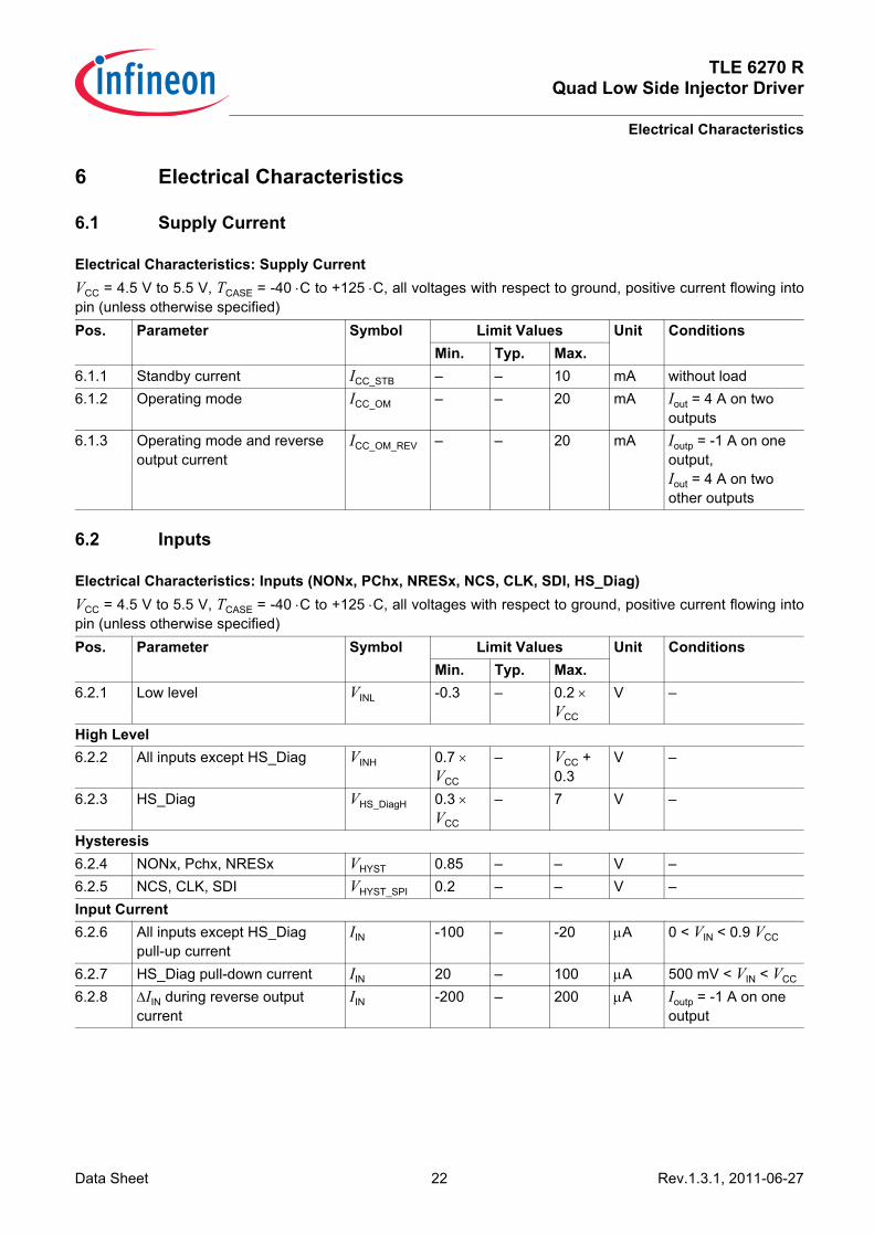
6.1 Supply Current
6.2 Inputs
Electrical Characteristics: Supply CurrentVCC = 4.5 V to 5.5 V, TCASE = -40 ⋅C to +125 ⋅C, all voltages with respect to ground, positive current flowing intopin (unless otherwise specified)Pos. Parameter Symbol Limit Values Unit Conditions
Min. Typ. Max.6.1.1 Standby current ICC_STB – – 10 mA without load6.1.2 Operating mode ICC_OM – – 20 mA Iout = 4 A on two
outputs6.1.3 Operating mode and reverse
output currentICC_OM_REV – – 20 mA Ioutp = -1 A on one
output,Iout = 4 A on two other outputs
Electrical Characteristics: Inputs (NONx, PChx, NRESx, NCS, CLK, SDI, HS_Diag)VCC = 4.5 V to 5.5 V, TCASE = -40 ⋅C to +125 ⋅C, all voltages with respect to ground, positive current flowing intopin (unless otherwise specified)Pos. Parameter Symbol Limit Values Unit Conditions
Min. Typ. Max.6.2.1 Low level VINL -0.3 – 0.2 ×
VCC
V –
High Level6.2.2 All inputs except HS_Diag VINH 0.7 ×
VCC
– VCC + 0.3
V –
6.2.3 HS_Diag VHS_DiagH 0.3 × VCC
– 7 V –
Hysteresis6.2.4 NONx, Pchx, NRESx VHYST 0.85 – – V –6.2.5 NCS, CLK, SDI VHYST_SPI 0.2 – – V –Input Current6.2.6 All inputs except HS_Diag
pull-up currentIIN -100 – -20 μA 0 < VIN < 0.9 VCC
6.2.7 HS_Diag pull-down current IIN 20 – 100 μA 500 mV < VIN < VCC
6.2.8 ΔIIN during reverse output current
IIN -200 – 200 μA Ioutp = -1 A on one output
Data Sheet 22 Rev.1.3.1, 2011-06-27

TLE 6270 RQuad Low Side Injector Driver
Electrical Characteristics
6.3 Outputs
Electrical Characteristics: Serial Data Output (SDO)VCC = 4.5 V to 5.5 V, TCASE = -40 ⋅C to +125 ⋅C, all voltages with respect to ground, positive current flowing intopin (unless otherwise specified)Pos. Parameter Symbol Limit Values Unit Conditions
Min. Typ. Max.6.3.1 High output level VSDOH VCC -
0.4– – V ISDO = -2 mA
6.3.2 Low output level VSDOL – – 0.4 V ISDO = 3.2 mA6.3.3 Tristate leakage current ISDOL -10 – 10 μA NCS = HIGH;
VSDO = 0 … VCC
Electrical Characteristics: Control HS Outputs (NCTLx)VCC = 4.5 V to 5.5 V, TCASE = -40 ⋅C to +125 ⋅C, all voltages with respect to ground, positive current flowing intopin (unless otherwise specified)Pos. Parameter Symbol Limit Values Unit Conditions
Min. Typ. Max.6.3.4 High output level VNCTLH VCC - 1 – – V INCTL = -10 mA6.3.5 Low output level VNCTLL – – 0.1 V INCTL = 1 mA6.3.6 Peak current at L → H transition IP_NCTL_LH – – -35 mA VNCTL = VCC - 4 V6.3.7 Peak current at H → L transition IP_NCTL_HL 40 – – mA VNCTL = 4 V
Electrical Characteristics: Power Outputs (OUTx)VCC = 4.5 V to 5.5 V, TCASE = -40 ⋅C to +125 ⋅C, all voltages with respect to ground, positive current flowing intopin (unless otherwise specified)Pos. Parameter Symbol Limit Values Unit Conditions
Min. Typ. Max.6.3.8 ON resistance at VCC = 5 V RDSON1 – – 300 mΩ 1)
Iout = 5 A;VCC = 5 V;Tj = 150 °C
6.3.9 Clamp voltage VCLP1 80 87 94 V 1)
IOUT = 4 A6.3.10 Clamp voltage at -1 A on neighbor
outputVCLPR – – 94 V test current 100 mA
6.3.11 Matching clamp voltage VCLPM VCLP - 7 – VCLP + 7
V –
6.3.12 Leakage current IOUTL – – 10 μA VOUT = 18 V6.3.13 Neg. output voltage ramp
(75% × Vbat … 25% × Vbat, inductive load)
OVRn – 20 100 V/μs see Chapter 7.21)2)
6.3.14 Pos. output voltage ramp(25% × Vbat … 70 V, inductive load)
OVRp – 100 200 V/μs see Chapter 7.2 1)2)3)
Data Sheet 23 Rev.1.3.1, 2011-06-27
TLE 6270 RQuad Low Side Injector Driver
Electrical Characteristics
6.3.15 Turn ON delay(NON 50%; Vout = 25% × Vbat inductive load)
tdON 1.5 μs see Chapter 7.21)2)
6.3.16 Turn OFF delay (NON 50%; Vout = 70 V, inductive load)
tdOFF 1.5 μs see Chapter 7.21)2)
1) Characteristics tested in different conditions than the specification and guaranteed by correlation.2) Measured with resistive load.3) The design is optimized for low EM emissions (no clamp overshoot).
Electrical Characteristics: Power Outputs Reverse DiodeVCC = 4.5 V to 5.5 V, TCASE = -40 ⋅C to +125 ⋅C, all voltages with respect to ground, positive current flowing intopin (unless otherwise specified)Pos. Parameter Symbol Limit Values Unit Conditions
Min. Typ. Max.6.3.17 Reverse voltage drop VRDa 0.8 – 1.5 V for Iout = -5.0 A
(200 μs pulse)6.3.18 Reverse voltage drop VRDb 0.6 – 1.5 V for Iout = -2.5 A
(200 μs pulse)
Electrical Characteristics: Power Outputs (OUTx) (cont’d)VCC = 4.5 V to 5.5 V, TCASE = -40 ⋅C to +125 ⋅C, all voltages with respect to ground, positive current flowing intopin (unless otherwise specified)Pos. Parameter Symbol Limit Values Unit Conditions
Min. Typ. Max.
Data Sheet 24 Rev.1.3.1, 2011-06-27
TLE 6270 RQuad Low Side Injector Driver
Electrical Characteristics
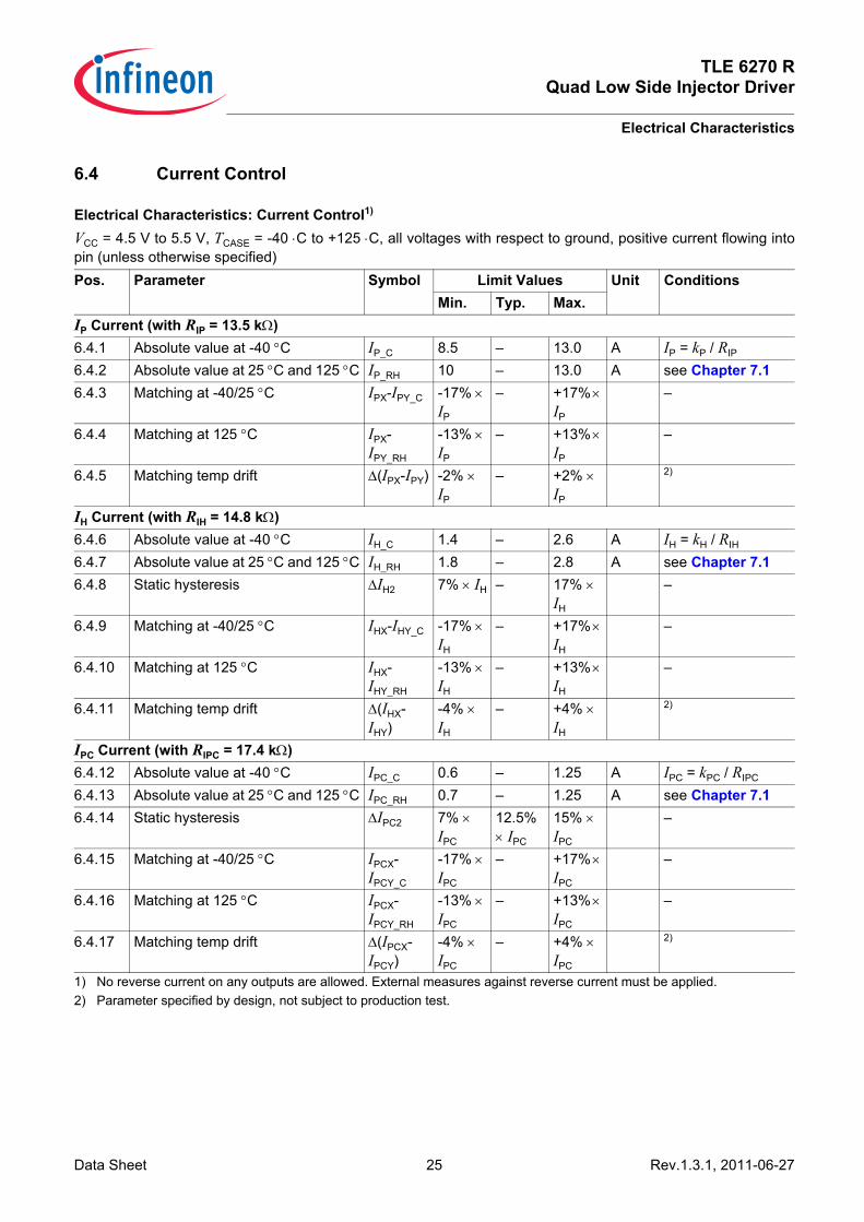
6.4 Current Control
Electrical Characteristics: Current Control1)
VCC = 4.5 V to 5.5 V, TCASE = -40 ⋅C to +125 ⋅C, all voltages with respect to ground, positive current flowing intopin (unless otherwise specified)
1) No reverse current on any outputs are allowed. External measures against reverse current must be applied.
Pos. Parameter Symbol Limit Values Unit ConditionsMin. Typ. Max.
IP Current (with RIP = 13.5 kΩ)6.4.1 Absolute value at -40 °C IP_C 8.5 – 13.0 A IP = kP / RIP
6.4.2 Absolute value at 25 °C and 125 °C IP_RH 10 – 13.0 A see Chapter 7.16.4.3 Matching at -40/25 °C IPX-IPY_C -17% ×
IP– +17% ×
IP–
6.4.4 Matching at 125 °C IPX-IPY_RH
-13% × IP
– +13% × IP
–
6.4.5 Matching temp drift Δ(IPX-IPY) -2% × IP
– +2% × IP
2)
2) Parameter specified by design, not subject to production test.
IH Current (with RIH = 14.8 kΩ)6.4.6 Absolute value at -40 °C IH_C 1.4 – 2.6 A IH = kH / RIH
6.4.7 Absolute value at 25 °C and 125 °C IH_RH 1.8 – 2.8 A see Chapter 7.16.4.8 Static hysteresis ΔIH2 7% × IH – 17% ×
IH–
6.4.9 Matching at -40/25 °C IHX-IHY_C -17% × IH
– +17% × IH
–
6.4.10 Matching at 125 °C IHX-IHY_RH
-13% × IH
– +13% × IH
–
6.4.11 Matching temp drift Δ(IHX-IHY)
-4% × IH
– +4% × IH
2)
IPC Current (with RIPC = 17.4 kΩ)6.4.12 Absolute value at -40 °C IPC_C 0.6 – 1.25 A IPC = kPC / RIPC
6.4.13 Absolute value at 25 °C and 125 °C IPC_RH 0.7 – 1.25 A see Chapter 7.16.4.14 Static hysteresis ΔIPC2 7% ×
IPC
12.5% × IPC
15% × IPC
–
6.4.15 Matching at -40/25 °C IPCX-IPCY_C
-17% × IPC
– +17% × IPC
–
6.4.16 Matching at 125 °C IPCX-IPCY_RH
-13% × IPC
– +13% × IPC
–
6.4.17 Matching temp drift Δ(IPCX-IPCY)
-4% × IPC
– +4% × IPC
2)
Data Sheet 25 Rev.1.3.1, 2011-06-27

TLE 6270 RQuad Low Side Injector Driver
Electrical Characteristics
6.5 Current Control Timings
6.6 Diagnostic and Protections
Electrical Characteristics: Current Control Timings (Load capacitor at NCTLx = 100 pF)VCC = 4.5 V to 5.5 V, TCASE = -40 ⋅C to +125 ⋅C, all voltages with respect to ground, positive current flowing intopin (unless otherwise specified)Pos. Parameter Symbol Limit Values Unit Conditions
Min. Typ. Max.NCTL2 Current Control Delay6.5.1 delay from Pch14 50% × VCC
to NCTL2 50% × VCC
tdNCTL2a – – 200 ns –
6.5.2 delay from HS_diag 50% × VCCto NCTL2 50% × VCC
tdNCTL2c – – 500 ns –
NCTL3 Current Control Delay6.5.3 delay from HS_diag 50% × VCC
to NCTL3 50% × VCC
tdNCTL3c – – 500 ns –
Electrical Characteristics: Diagnostic and ProtectionsVCC = 4.5 V to 5.5 V, TCASE = -40 ⋅C to +125 ⋅C, all voltages with respect to ground, positive current flowing intopin (unless otherwise specified)Pos. Parameter Symbol Limit Values Unit Conditions
Min. Typ. Max.6.6.1 Overcurrent threshold IOFF 1.18 ×
IP1.4 × IP 1.62 ×
IPA 1)
1) Not subject to production test, specified by design.
6.6.2 Overtemperature threshold TOFF 155 – 185 °C 2)3)
2) Characteristics tested at wafer level only (with special testpads), not on packaged parts.3) Characteristics tested in different conditions than the specification and guaranteed by correlation.
6.6.3 HS diag input: filter and setup time tHS 50 – 250 ns –6.6.4 Overcurrent / Overtemperature
Shutdown filter and delay timetOFF 8 – 18 μs 1)
6.6.5 Pull-up resistor RPULL-UP 40 – 150 kΩ –6.6.6 OFF state overvoltage threshold VOL 0.6 ×
VCC
– 0.7 × VCC
V –
6.6.7 OFF state overvoltage filter and delay time
tOL 3.5 – 4.5 ms –
6.6.8 Peak current overtime threshold tPmax – t1 – μs –6.6.9 Peak current undertime threshold tPmin 10 – 60 μs –6.6.10 VCC undervoltage VCCRES 3.35 – 3.95 V –6.6.11 Undervoltage protection
Max ON-time after a output voltage ramp from:0 V to 25 V at VCC = 0 V to 5.5 V
trpON – – 100 μs –
Data Sheet 26 Rev.1.3.1, 2011-06-27
TLE 6270 RQuad Low Side Injector Driver
Electrical Characteristics
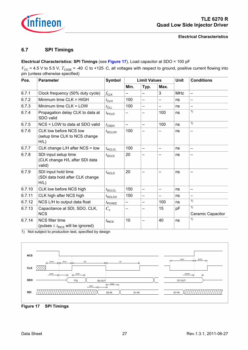
6.7 SPI Timings
Figure 17 SPI Timings
Electrical Characteristics: SPI Timings (see Figure 17), Load capacitor at SDO = 100 pFVCC = 4.5 V to 5.5 V, TCASE = -40 ⋅C to +125 ⋅C, all voltages with respect to ground, positive current flowing intopin (unless otherwise specified)Pos. Parameter Symbol Limit Values Unit Conditions
Min. Typ. Max.6.7.1 Clock frequency (50% duty cycle) fCLK – – 3 MHz –6.7.2 Minimum time CLK = HIGH tCLH 100 – – ns –6.7.3 Minimum time CLK = LOW tCLL 100 – – ns –6.7.4 Propagation delay CLK to data at
SDO validtPCLD – – 100 ns 1)
6.7.5 NCS = LOW to data at SDO valid tCSDV – – 100 ns 1)
1) Not subject to production test, specified by design
6.7.6 CLK low before NCS low (setup time CLK to NCS change H/L)
tSCLCH 100 – – ns –
6.7.7 CLK change L/H after NCS = low tHCLCL 100 – – ns –6.7.8 SDI input setup time
(CLK change H/L after SDI data valid)
tSCLD 20 – – ns –
6.7.9 SDI input hold time(SDI data hold after CLK change H/L)
tHCLD 20 – – ns –
6.7.10 CLK low before NCS high tSCLCL 150 – – ns –6.7.11 CLK high after NCS high tHCLCH 150 – – ns –6.7.12 NCS L/H to output data float tPCHDZ – – 100 ns 1)
6.7.13 Capacitance at SDI, SDO, CLK, NCS
Cx – – 15 pF 1)
Ceramic Capacitor6.7.14 NCS filter time
(pulses ≤ tfNCS will be ignored)tfNCS 10 – 40 ns 1)
thclchtsclcltclltclhtsclch thclcl
NCS
CLK
SDO
SDI
FSL
tcsdv tpcld
D0-OUT
tscldthcld
D0-IN D1-IN D7-IN
D7-OUT
tpchdz
Data Sheet 27 Rev.1.3.1, 2011-06-27

TLE 6270 RQuad Low Side Injector Driver
Electrical Characteristics
Attention: To avoid any unknown logic state, t1 and t2 values must be latched at the end of t2 time. Moreover, one latch is needed for each group (A and B) for overlapping reasons. At last, as t1 and t2 can be whenever changed, t1 and t2 should be stored in TLE6270R to release the SPI bus prior to being taken into account by the internal counters.
Figure 18 Application Hint: Example of Resonator
Electrical Characteristics: Internal Clock(see SMD ceramic resonator specification n° S108 058 007 / 65 92 36.20.89, Figure 18)VCC = 4.5 V to 5.5 V, TCASE = -40 ⋅C to +125 ⋅C, all voltages with respect to ground, positive current flowing intopin (unless otherwise specified)Pos. Parameter Symbol Limit Values Unit Conditions
Min. Typ. Max.6.7.15 External resonator frequency fOSC – 8 – MHz –6.7.16 Internal frequency tolerance ΔfOSC -3% – +3% fOSC –
Electrical Characteristics: Programmable TimingsVCC = 4.5 V to 5.5 V, TCASE = -40 ⋅C to +125 ⋅C, all voltages with respect to ground, positive current flowing intopin (unless otherwise specified)Pos. Parameter Symbol Limit Values Unit Conditions
Min. Typ. Max.t1 Time6.7.17 Number of coding bit via SPI – 3 – –6.7.18 t1 default value t1_0 – 192 – μs (0, 0, 0)6.7.19 t1 LSB (Least Significant Bit) t1_lsb – 32 – μs –6.7.20 t1 max value t1_max – 416 – μs (1, 1, 1)t2 Time6.7.21 Number of coding bit via SPI – 5 – –6.7.22 t2 default value t2_0 – 0 – μs (0, 0, 0, 0, 0)6.7.23 t2 LSB (Least Significant Bit) t2_lsb – 2 – μs –6.7.24 t2 max value t2_max – 62 – μs (1, 1, 1, 1, 1)
ResonatorElectrical CharacteristicsNominal Oscillating Frequency 8.000MHzOscillating Frequency Tolerance +/-0.5%Built-in Capacitance value 30pF +/-20%Resonant Impedance
Maximum Resonant Impedance 40Ohm max.Variation by Temperature Change 10Ohm max. at 170°C, 6sec.
Insulation Resistance 500MOhm min (at 10VDC)Withstanding Voltage 100VDC, 5 sec. max.Absolute Maximum Voltage
Maximum DC Voltage 6VDCMaximum Input Voltage 15Vpp
Temperature Characteristic (-40 to +125°C) +/-0.4% max.Operating Temperature Range -40 to +125°CStorage Temperature Range -55 to +125°C
Application Diagram
Data Sheet 28 Rev.1.3.1, 2011-06-27

TLE 6270 RQuad Low Side Injector Driver
Diagrams
7 Diagrams
7.1 Typical Laws
Figure 19 IP(RIP) (temp = 25 °C)
Figure 20 IPC(RIPC) (temp = 25 °C)
Figure 21 IH(RIH) (temp = 25 °C)
IP=f(RIP)
y = 155/x
99,510
10,511
11,512
12,513
11,0 12,0 13,0 14,0 15,0 16,0 17,0 18,0RIP (kohm)
IP(A)
IPC=f(RIPC)y = 17,4/x
0,8
0,85
0,9
0,95
1
1,05
1,1
1,15
1,2
14,0 15,0 16,0 17,0 18,0 19,0 20,0 21,0 22,0
RIP (kohm)
IPC(A)
IH=f(RIH)y = 32,5/x
1,8
2
2,2
2,4
2,6
2,8
3
3,2
3,4
3,6
9,0 10,0 11,0 12,0 13,0 14,0 15,0 16,0 17,0 18,0 19,0
RIH (kohm)
IH(A)
Data Sheet 29 Rev.1.3.1, 2011-06-27
TLE 6270 RQuad Low Side Injector Driver
Diagrams
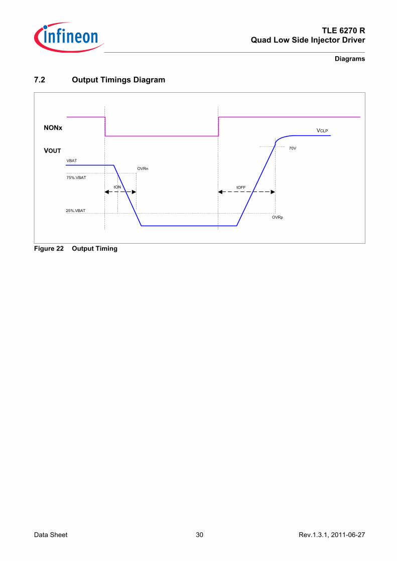
7.2 Output Timings Diagram
Figure 22 Output Timing
VOUT
VCLPNONx
25%.VBAT
75%.VBAT
VBAT
OVRn
OVRp
tON tOFF
70V
Data Sheet 30 Rev.1.3.1, 2011-06-27
TLE 6270 RQuad Low Side Injector Driver
Application Information
8 Application InformationNote: The following information is given as a hint for the implementation of the device only and shall not be
regarded as a description or warranty of a certain functionality, condition or quality of the device.
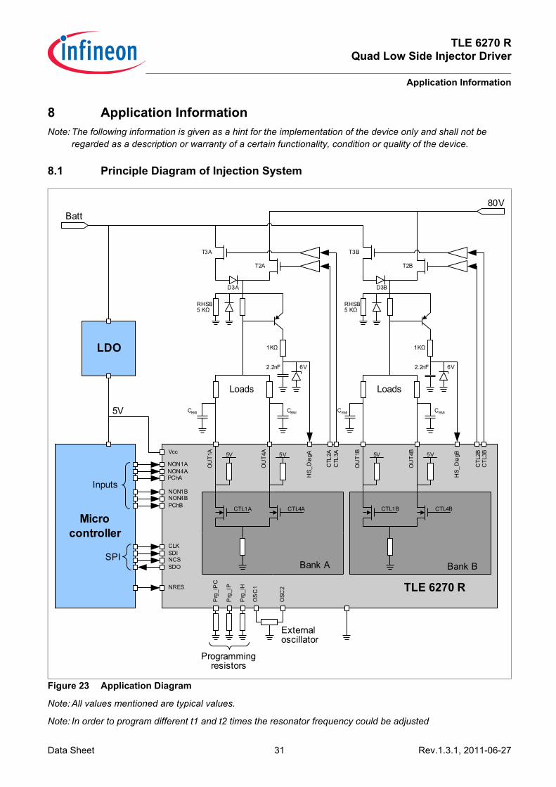
8.1 Principle Diagram of Injection System
Figure 23 Application Diagram
Note: All values mentioned are typical values.
Note: In order to program different t1 and t2 times the resonator frequency could be adjusted
TLE 6270 R
Loads Loads
Programming resistors
External oscillator
RHSB5 KΩ
LDO
Batt80V
RHSB5 KΩ
Micro controller
5V
SPI
Inputs
SDO
NRES
CLKSDINCS
NON1ANON4APChA
NON1BNON4BPChB
Vcc
OU
T1A
OU
T4A
Prg
_IP
C
Prg
_IP
Prg
_IH
OS
C1
OSC
2
OU
T1B
OU
T4B
Bank A Bank B
HS_
Dia
gA
CTL
3AC
TL2A
CTL
3BC
TL2B
HS_
Dia
gB
T3A
T2A T2B
T3B
D3B
6V 6V2.2nF 2.2nF
1KΩ 1KΩ
CEMI CEMI CEMI CEMI
5V 5V 5V 5V
CTL1A CTL4A CTL1B CTL4B
D3A
Data Sheet 31 Rev.1.3.1, 2011-06-27
TLE 6270 RQuad Low Side Injector Driver
Application Information
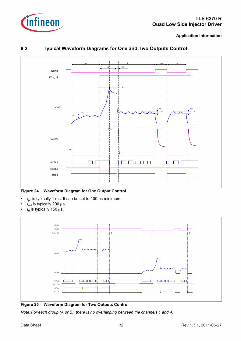
8.2 Typical Waveform Diagrams for One and Two Outputs Control
Figure 24 Waveform Diagram for One Output Control
• tpc is typically 1 ms. It can be set to 100 ns minimum.• twd is typically 200 μs.• td is typically 150 μs.
Figure 25 Waveform Diagram for Two Outputs Control
Note: For each group (A or B), there is no overlapping between the channels 1 and 4.
VCLP
tPC ti tWD tD
NON1
PCh_14
IOUT1
VOUT1
NCTL3
NCTL2
CTL1
IPC
ΔIPC
IP
IHΔIH
IDΔID
t1 t2
NON1
PCh_14
NCTL3
NCTL2
CTL1
CTL4
IOUT1
IOUT4
NON4
Data Sheet 32 Rev.1.3.1, 2011-06-27
TLE 6270 RQuad Low Side Injector Driver
Package Outlines
Data Sheet 33 Rev.1.3.1, 2011-06-27
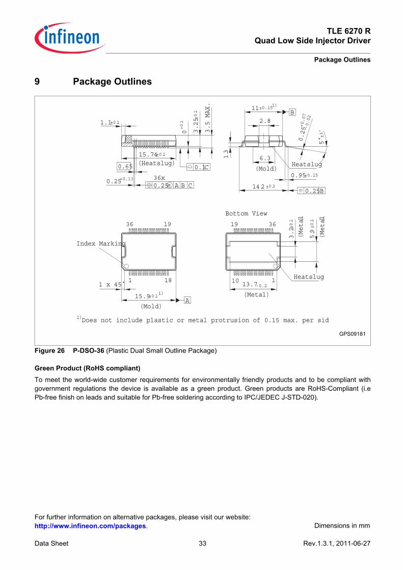
9 Package Outlines
Figure 26 P-DSO-36 (Plastic Dual Small Outline Package)
Green Product (RoHS compliant)To meet the world-wide customer requirements for environmentally friendly products and to be compliant withgovernment regulations the device is available as a green product. Green products are RoHS-Compliant (i.ePb-free finish on leads and suitable for Pb-free soldering according to IPC/JEDEC J-STD-020).
Bottom View
Does not include plastic or metal protrusion of 0.15 max. per sid
1 18
0.25
±0.11.1
36
+0.13
0.2536x
19
M
(Heatslug)15.74
0.65
±0.1
CA B
19
C
3.25
3.5 MAX.
+0.1
0
0.1
±0.1
36
2.8B
11±0.151)
1.3
5˚0.25
±3˚
-0.02
+0.07
6.3
14.2
(Mold)
±0.3B
±0.15
0.25
Heatslug
0.95
Heatslug
±0.1
5.9
3.2
(Metal)
±0.1
(Metal)
13.7
(Metal)
10 1-0.2
Index Marking
(Mold)
15.9 1)±0.1A
1 x 45˚
1)
GPS09181
For further information on alternative packages, please visit our website: http://www.infineon.com/packages. Dimensions in mm

Data Sheet 34 Rev.1.3.1, 2011-06-27
TLE 6270 RQuad Low Side Injector Driver
Revision History
10 Revision History
Revision Date Changes1.3.1 2011-06-27 Cover updated according to new template
Figure 1: editedFigure 23: edited, changed D3A, D3B placement
1.3 2008-10-22 Updated data sheet to newest template revisionFigure 1: changed Chapter 5.2: added detailsChapter 5.4.1: added paragraph regarding open load detectionTable 2: modifiedTable 3: modifiedFigure 15: modifiedTable 4: modifiedChapter 8: application information chapter movedFigure 23: changed and second note addedAll pages: editorial changes
1.1 2008-08-25 Initial version of RoHS-compliant derivate of TLE6270RDatasheet converted to green
Edition 2011-06-27Published byInfineon Technologies AG81726 Munich, Germany© 2011 Infineon Technologies AGAll Rights Reserved.
Legal DisclaimerThe information given in this document shall in no event be regarded as a guarantee of conditions or characteristics. With respect to any examples or hints given herein, any typical values stated herein and/or any information regarding the application of the device, Infineon Technologies hereby disclaims any and all warranties and liabilities of any kind, including without limitation, warranties of non-infringement of intellectual property rights of any third party.
InformationFor further information on technology, delivery terms and conditions and prices, please contact the nearest Infineon Technologies Office (www.infineon.com).
WarningsDue to technical requirements, components may contain dangerous substances. For information on the types in question, please contact the nearest Infineon Technologies Office.Infineon Technologies components may be used in life-support devices or systems only with the express written approval of Infineon Technologies, if a failure of such components can reasonably be expected to cause the failure of that life-support device or system or to affect the safety or effectiveness of that device or system. Life support devices or systems are intended to be implanted in the human body or to support and/or maintain and sustain and/or protect human life. If they fail, it is reasonable to assume that the health of the user or other persons may be endangered.


![Yamaha RX-V765 Htr-6270 Sm [ET]](https://static.documents.pub/doc/80x56/55cf968d550346d0338c3d71/yamaha-rx-v765-htr-6270-sm-et.jpg)


