TMS320C6201, TMS320C6201B DIGITAL SIGNAL PROCESSORS SPRS051D – JANUARY 1997 – REVISED AUGUST 1998 1 POST OFFICE BOX 1443 • HOUSTON, TEXAS 77251–1443 Highest Performance Fixed-Point Digital Signal Processor (DSP) TMS320C6201 – 5-ns Instruction Cycle Time – 200-MHz Clock Rate – Eight 32-Bit Instructions/Cycle – 1 600 MIPS Highest Performance Fixed-Point Digital Signal Processor (DSP) TMS320C6201B – 4.3-ns Instruction Cycle Time – 167-, 200-, and 233-MHz Clock Rates – Eight 32-Bit Instructions/Cycle – Over 1 860 MIPS VelociTIAdvanced Very Long Instruction Word (VLIW) ’C6200 CPU Core – Eight Independent Functional Units: – Six ALUs (32-/40-Bit) – Two 16-Bit Multipliers (32-Bit Results) – Load-Store Architecture With 32 32-Bit General-Purpose Registers – Instruction Packing Reduces Code Size – All Instructions Conditional Instruction Set Features – Byte-Addressable (8-, 16-, 32-Bit Data) – 32-Bit Address Range – 8-Bit Overflow Protection – Saturation – Bit-Field Extract, Set, Clear – Bit-Counting – Normalization 1M-Bit On-Chip SRAM – 512K-Bit Internal Program/Cache (16K 32-Bit Instructions) – 512K-Bit Dual-Access Internal Data (64K Bytes) Organized as a Single Block (’6201) – 512K-Bit Dual-Access Internal Data (64K Bytes) Organized as Two Blocks for Improved Concurrency (’6201B) 32-Bit External Memory Interface (EMIF) – Glueless Interface to Synchronous Memories: SDRAM and SBSRAM – Glueless Interface to Asynchronous Memories: SRAM and EPROM Four-Channel Bootloading Direct-Memory-Access (DMA) Controller with an Auxiliary Channel 16-Bit Host-Port Interface (HPI) – Access to Entire Memory Map Two Multichannel Buffered Serial Ports (McBSPs) – Direct Interface to T1/E1, MVIP, SCSA Framers – ST-Bus-Switching Compatible – Up to 256 Channels Each – AC97-Compatible – Serial Peripheral Interface (SPI) Compatible (Motorola) Two 32-Bit General-Purpose Timers Flexible Phase-Locked Loop (PLL) Clock Generator IEEE-1149.1 (JTAG ² ) Boundary-Scan Compatible 352-Pin BGA Package (GGP Suffix) (’6201) 352-Pin BGA Package (GJC Suffix) (’6201B) 352-Pin BGA Package (GJL Suffix) (’6201B) CMOS Technology – 0.25-μm/5-Level Metal Process (’6201) – 0.18-μm/5-Level Metal Process (’6201B) 3.3-V I/Os, 2.5-V Internal (’6201) 3.3-V I/Os, 1.8-V Internal (’6201B) Please be aware that an important notice concerning availability, standard warranty, and use in critical applications of Texas Instruments semiconductor products and disclaimers thereto appears at the end of this data sheet. VelociTI is a trademark of Texas Instruments Incorporated. Motorola is a trademark of Motorola, Inc. ² IEEE Standard 1149.1-1990 Standard-Test-Access Port and Boundary Scan Architecture. Copyright 1998, Texas Instruments Incorporated UNLESS OTHERWISE NOTED this document contains PRODUCTION DATA information current as of publication date. Products conform to specifications per the terms of Texas Instruments standard warranty. Production processing does not necessarily include testing of all parameters. GJC/GJL/GGP 352-PIN BALL GRID ARRAY (BGA) PACKAGES (BOTTOM VIEW) AF AD AB AA AC W Y U V AE R N P L H J K M F G D E B A C T 25 26 22 23 20 19 21 17 15 16 12 13 14 18 10 9 8 7 5 6 4 3 2 1 11 24
Transcript
TMS320C6201, TMS320C6201BDIGITAL SIGNAL PROCESSORS
(16K 32-Bit Instructions)– 512K-Bit Dual-Access Internal Data
(64K Bytes) Organized as a Single Block(’6201)
– 512K-Bit Dual-Access Internal Data(64K Bytes) Organized as Two Blocks forImproved Concurrency (’6201B)
32-Bit External Memory Interface (EMIF)– Glueless Interface to Synchronous
Memories: SDRAM and SBSRAM– Glueless Interface to Asynchronous
Memories: SRAM and EPROM
Four-Channel BootloadingDirect-Memory-Access (DMA) Controllerwith an Auxiliary Channel
16-Bit Host-Port Interface (HPI)– Access to Entire Memory Map
Two Multichannel Buffered Serial Ports(McBSPs)– Direct Interface to T1/E1, MVIP, SCSA
Framers– ST-Bus-Switching Compatible– Up to 256 Channels Each– AC97-Compatible– Serial Peripheral Interface (SPI)
Compatible (Motorola )
Two 32-Bit General-Purpose Timers
Flexible Phase-Locked Loop (PLL) ClockGenerator
IEEE-1149.1 (JTAG†) Boundary-ScanCompatible
352-Pin BGA Package (GGP Suffix) (’6201)
352-Pin BGA Package (GJC Suffix) (’6201B)
352-Pin BGA Package (GJL Suffix) (’6201B)
CMOS Technology– 0.25-µm/5-Level Metal Process (’6201)– 0.18-µm/5-Level Metal Process (’6201B)
3.3-V I/Os, 2.5-V Internal (’6201)
3.3-V I/Os, 1.8-V Internal (’6201B)
Please be aware that an important notice concerning availability, standard warranty, and use in critical applications ofTexas Instruments semiconductor products and disclaimers thereto appears at the end of this data sheet.
VelociTI is a trademark of Texas Instruments Incorporated.Motorola is a trademark of Motorola, Inc.† IEEE Standard 1149.1-1990 Standard-Test-Access Port and Boundary Scan Architecture.
Copyright 1998, Texas Instruments IncorporatedUNLESS OTHERWISE NOTED this document contains PRODUCTIONDATA information current as of publication date. Products conform tospecifications per the terms of Texas Instruments standard warranty.Production processing does not necessarily include testing of allparameters.
GJC/GJL/GGP352-PIN BALL GRID ARRAY (BGA) PACKAGES
(BOTTOM VIEW)
AF
AD
ABAA
AC
WY
UV
AE
R
NP
L
HJK
M
FG
DE
BA
C
T
252622
2320
19 2117151612
1314 1810
98
7564
32
1 1124
TMS320C6201, TMS320C6201BDIGITAL SIGNAL PROCESSORS
SPRS051D – JANUARY 1997 – REVISED AUGUST 1998
2 POST OFFICE BOX 1443 • HOUSTON, TEXAS 77251–1443
Signal DescriptionsSIGNAL
†NAME
GGP, GJCPIN NO.
GJL PIN NO.
TYPE† DESCRIPTION
CLOCK/PLL
CLKIN C10 B9 I Clock Input
CLKOUT1 AF22 AC18 O Clock output at full device speed
CLKOUT2 AF20 AC16 O Clock output at half of device speed
CLKMODE1 C6 D8I
Clock-mode select
CLKMODE0 C5 C7I
• Selects whether the CPU clock frequency = input clock frequency x4 or x1
PLLFREQ3 A9 A9 PLL frequency range (3, 2, and 1)
PLLFREQ2 D11 D11 I• The target range for CLKOUT1 frequency is determined by the 3-bit value of thePLLFREQ pins.
PLLFREQ1 B10 B10
PLLV‡ D12 B11 A§ PLL analog VCC connection for the low-pass filter
PLLG‡ C12 C12 A§ PLL analog GND connection for the low-pass filter
PLLF A11 D12 A§ PLL low-pass filter connection to external components and a bypass capacitor
JTAG EMULATION
TMS L3 L3 I JTAG test port mode select (features an internal pullup)
TDO W2 U4 O/Z JTAG test port data out
TDI R4 T2 I JTAG test port data in (features an internal pullup)
TCK R3 R3 I JTAG test port clock
TRST T1 R4 I JTAG test port reset (features an internal pulldown)
EMU1 Y1 V3 I/O/Z Emulation pin 1, pullup with a dedicated 20-kΩ resistor
EMU0 W3 W2 I/O/Z Emulation pin 0, pullup with a dedicated 20-kΩ resistor
IACK Y2 Y1 O Interrupt acknowledge for all active interrupts serviced by the CPU
INUM3 AA1 V4
INUM2 W4 Y2O
Active interrupt identification number• Valid during IACK for all active interrupts (not just external)
INUM1 AA2 AA1O • Valid during IACK for all active interrupts (not just external)
• Encoding order follows the interrupt-service fetch-packet orderingINUM0 AB1 W4
• Encoding order follows the interru t service fetch acket ordering
LITTLE ENDIAN/BIG ENDIAN
LENDIAN H3 G2 IIf high, LENDIAN selects little-endian byte/half-word addressing order within a wordIf low, LENDIAN selects big-endian addressing
POWER-DOWN STATUS
PD D3 E2 O Power-down mode 2 or 3 (active if high)† I = Input, O = Output, Z = High Impedance, S = Supply Voltage, GND = Ground‡ PLLV and PLLG are not part of external voltage supply or ground. See the clock PLL section for information on how to connect these pins.§ A = Analog Signal (PLL Filter)
TMS320C6201, TMS320C6201BDIGITAL SIGNAL PROCESSORS
SPRS051D – JANUARY 1997 – REVISED AUGUST 1998
3POST OFFICE BOX 1443 • HOUSTON, TEXAS 77251–1443
Signal Descriptions (Continued)SIGNAL
†NAME
GGP, GJCPIN NO.
GJL PIN NO.
TYPE† DESCRIPTION
HOST-PORT INTERFACE (HPI)
HINT H26 J26 O Host interrupt (from DSP to host)
HCNTL1 F23 G24 I Host control – selects between control, address, or data registers
HCNTL0 D25 F25 I Host control – selects between control, address, or data registers
HHWIL C26 E26 I Host half-word select – first or second half-word (not necessarily high or low order)
HBE1 E23 F24 I Host byte select within word or half-word
HBE0 D24 E25 I Host byte select within word or half-word
HR/W C23 B22 I Host read or write select
HD15 B13 A12
HD14 B14 D13
HD13 C14 C13
HD12 B15 D14
HD11 D15 B15
HD10 B16 C15
HD9 A17 D15
HD8 B17 B16I/O/Z Host port data (used for transfer of data address and control)
HD7 D16 C16I/O/Z Host-port data (used for transfer of data, address, and control)
HD6 B18 B17
HD5 A19 D16
HD4 C18 A18
HD3 B19 B18
HD2 C19 D17
HD1 B20 C18
HD0 B21 A20
HAS C22 C20 I Host address strobe
HCS B23 B21 I Host chip select
HDS1 D22 C21 I Host data strobe 1
HDS2 A24 D20 I Host data strobe 2
HRDY J24 J25 O Host ready (from DSP to host)
BOOT MODE
BOOTMODE4 D8 C8
BOOTMODE3 B4 B6
BOOTMODE2 A3 D7 I Boot mode
BOOTMODE1 D5 C6
BOOTMODE0 C4 B5† I = Input, O = Output, Z = High Impedance, S = Supply Voltage, GND = Ground
TMS320C6201, TMS320C6201BDIGITAL SIGNAL PROCESSORS
SPRS051D – JANUARY 1997 – REVISED AUGUST 1998
4 POST OFFICE BOX 1443 • HOUSTON, TEXAS 77251–1443
Signal Descriptions (Continued)SIGNAL
†NAME
GGP, GJCPIN NO.
GJL PIN NO.
TYPE† DESCRIPTION
EMIF – CONTROL SIGNALS COMMON TO ALL TYPES OF MEMORY
CE3 AE22 AD20
CE2 AD26 AA24O/Z
Memory space enables
CE1 AB24 AB26O/Z
• Enabled by bits 24 and 25 of the word address
CE0 AC26 AA25 • Only one asserted during any external data access
BE3 AB25 Y24 Byte-enable control
BE2 AA24 W23O/Z
• Decoded from the two lowest bits of the internal address
BE1 Y23 AA26O/Z
• Byte-write enables for most types of memory
BE0 AA26 W25 • Can be directly connected to SDRAM read and write mask signal (SDQM)
EMIF – ADDRESS
EA21 J26 K25
EA20 K25 L24
EA19 L24 L25
EA18 K26 M23
EA17 M26 M25
EA16 M25 M24
EA15 P25 N23
EA14 P24 P24
EA13 R25 P23
EA12 T26 R25O/Z External address (word address)
EA11 R23 R24O/Z External address (word address)
EA10 U26 R23
EA9 U25 T25
EA8 T23 T24
EA7 V26 U25
EA6 V25 T23
EA5 W26 V26
EA4 V24 V25
EA3 W25 U23
EA2 Y26 V24† I = Input, O = Output, Z = High Impedance, S = Supply Voltage, GND = Ground
TMS320C6201, TMS320C6201BDIGITAL SIGNAL PROCESSORS
TMS320C6201, TMS320C6201BDIGITAL SIGNAL PROCESSORS
SPRS051D – JANUARY 1997 – REVISED AUGUST 1998
16 POST OFFICE BOX 1443 • HOUSTON, TEXAS 77251–1443
CPU description
The CPU fetches VelociTI advanced very-long instruction words (VLIW) (256 bits wide) to supply up to eight32-bit instructions to the eight functional units during every clock cycle. The VelociTI VLIW architecture featurescontrols by which all eight units do not have to be supplied with instructions if they are not ready to execute. Thefirst bit of every 32-bit instruction determines if the next instruction belongs to the same execute packet as theprevious instruction, or whether it should be executed in the following clock as a part of the next execute packet.Fetch packets are always 256 bits wide; however, the execute packets can vary in size. The variable-lengthexecute packets are a key memory-saving feature, distinguishing the ’C6200† CPU from other VLIWarchitectures.
The CPU features two sets of functional units. Each set contains four units and a register file. One set containsfunctional units .L1, .S1, .M1, and .D1; the other set contains units .D2, .M2, .S2, and .L2. The two register fileseach contain 16 32-bit registers for a total of 32 general-purpose registers. The two sets of functional units, alongwith two register files, compose sides A and B of the CPU (see Figure 3 and Figure 4). The four functional unitson each side of the CPU can freely share the 16 registers belonging to that side. Additionally, each side featuresa single data bus connected to all the registers on the other side, by which the two sets of functional units canaccess data from the register files on the opposite side. While register access by functional units on the sameside of the CPU as the register file can service all the units in a single clock cycle, register access using theregister file across the CPU supports one read and one write per cycle.
Another key feature of the ’C6200 CPU is the load/store architecture, where all instructions operate on registers(as opposed to data in memory). Two sets of data-addressing units (.D1 and .D2) are responsible for all datatransfers between the register files and the memory. The data address driven by the .D units allows dataaddresses generated from one register file to be used to load or store data to or from the other register file. The’C6200 CPU supports a variety of indirect addressing modes using either linear- or circular-addressing modeswith 5- or 15-bit offsets. All instructions are conditional, and most can access any one of the 32 registers. Someregisters, however, are singled out to support specific addressing or to hold the condition for conditionalinstructions (if the condition is not automatically “true”). The two .M functional units are dedicated for multiplies.The two .S and .L functional units perform a general set of arithmetic, logical, and branch functions with resultsavailable every clock cycle.
The processing flow begins when a 256-bit-wide instruction fetch packet is fetched from a program memory.The 32-bit instructions destined for the individual functional units are “linked” together by “1” bits in the leastsignificant bit (LSB) position of the instructions. The instructions that are “chained” together for simultaneousexecution (up to eight in total) compose an execute packet. A “0” in the LSB of an instruction breaks the chain,effectively placing the instructions that follow it in the next execute packet. If an execute packet crosses the fetchpacket boundary (256 bits wide), the assembler places it in the next fetch packet, while the remainder of thecurrent fetch packet is padded with NOP instructions. The number of execute packets within a fetch packet canvary from one to eight. Execute packets are dispatched to their respective functional units at the rate of one perclock cycle and the next 256-bit fetch packet is not fetched until all the execute packets from the current fetchpacket have been dispatched. After decoding, the instructions simultaneously drive all active functional unitsfor a maximum execution rate of eight instructions every clock cycle. While most results are stored in 32-bitregisters, they can be subsequently moved to memory as bytes or half-words as well. All load and storeinstructions are byte-, half-word, or word-addressable.
† Where unique device characteristics are specified, TMS320C6201 and TMS320C6201B identifiers are used. For generic characteristics, noidentifiers are needed, ’C62xx is used, or ’C6200 is used.
TMS320C6201, TMS320C6201BDIGITAL SIGNAL PROCESSORS
All of the ’C62xx clocks are generated from a single source through the CLKIN pin. This source clock eitherdrives the PLL, which generates the internal CPU clock, or bypasses the PLL to become the CPU clock.
To use the PLL to generate the CPU clock, the filter circuit shown in Figure 5 must be properly designed. Notethat for ’C6201, the EMI filter must be powered by the core voltage (2.5 V), and for ’C6201B, it must be poweredby the I/O voltage (3.3 V).
To configure the ’C62xx PLL clock for proper operation, see Figure 5 and Table 1. To minimize the clock jitter,a single clean power supply should power both the ’C62x device and the external clock oscillator circuit. Theminimum CLKIN rise and fall times should also be observed. See the input and output clocks section for inputclock timing requirements.
CLKIN
PLLV
PLLF
PLLG
0 1 0 – ’C6201B CLKOUT1 Frequency Range 130–233 MHz
0 0 1 – ’C6201B CLKOUT1 Frequency Range 65–200 MHz
0 0 0 – ’C6201B CLKOUT1 Frequency Range 50–140 MHz
PLL
FR
EQ
3
’C6201 CLKOUT1 Frequency Range 40–200 MHz –
’C6201 CLKOUT1 Frequency Range 35–160 MHz –
’C6201 CLKOUT1 Frequency Range 25–135 MHz –
PLL
FR
EQ
2P
LLF
RE
Q1
CLKOUT
1 1
0 1
1 0
0 0
– MULT ×4
– Reserved
– Reserved
– MULT ×1
f(CLKOUT)= f(CLKIN) ×4
f(CLKOUT)= f(CLKIN)
10 µF 0.1 µF(Bypass)
C1 C2
R1
3.3 VC
LKM
OD
E0
CLK
MO
DE
1
CLKOUT1
CLKOUT2
SSCLK
SDCLK
EMIF
’320C6201/C6201B2.5 V
GND
21 IN
3 OUT
EM
I Filt
er
NOTES: A. For the ’C6201 CLKMODE x4, values for C1, C2, and R1 depend on CLKIN and CLKOUT frequencies.For the ’C6201B CLKMODE x4, values for C1, C2, and R1 are fixed and apply to all valid frequency ranges of CLKIN and CLKOUT.
B. For CLKMODE x1, the PLL is bypassed and all six external PLL components can be removed. For this case, the PLLV terminal hasto be connected to a clean supply and the PLLG and PLLF terminals should be tied together.
C. Due to overlap of frequency ranges when choosing the PLLFREQ, more than one frequency range can contain the CLKOUT1frequency. Choose the lowest frequency range that includes the desired frequency. For example, CLKOUT1 = 133 MHz, aPLLFREQ value of 000b should be used for both the ’C6201 and the ’C6201B. For CLKOUT1 = 200 MHz, PLLFREQ should be setto 010b for the ’C6201 or 001b for the ’C6201B. PLLFREQ values other than 000b, 001b, and 010b are reserved.
D. EMI filter manufacturer TDK part number ACF451832-153-TE. For the ’C6201B, the 3.3-V supply for the EMI filter (and PLLV) must be from the same 3.3-V power plane supplying the I/O voltage,
DVDD.
Figure 5. PLL Block Diagram
TMS320C6201, TMS320C6201BDIGITAL SIGNAL PROCESSORS
SPRS051D – JANUARY 1997 – REVISED AUGUST 1998
20 POST OFFICE BOX 1443 • HOUSTON, TEXAS 77251–1443
10 x4 25 100 10 0.47 8200 TDK #153 68† For CLKMODE x1, the PLL is bypassed and all six external PLL components can be removed. For this case, the PLLV terminal has to be
connected to a clean supply and the PLLG and PLLF terminals should be tied together.‡ Full EMI filter part number : ACF 451832-153-T§ Under some operating conditions, the maximum PLL lock time may vary as much as 150% from the specified typical value. For example, if the
typical lock time is specified as 100 µs, the maximum value may be as long as 250 µs.
x4 60.4 27 560 TDK #153 75† For CLKMODE x1, the PLL is bypassed and all six external PLL components can be removed. For this case, the PLLV terminal has to be
connected to a clean supply and the PLLG and PLLF terminals should be tied together.‡ Full EMI filter part number : ACF 451832-153-T§ Under some operating conditions, the maximum PLL lock time may vary as much as 150% from the specified typical value. For example, if the
typical lock time is specified as 100 µs, the maximum value may be as long as 250 µs.
power supply sequencing
For the ’C6201 device, the 2.5-V supply powers the core and the 3.3-V supply powers the I/O buffers. For the’C6201B device, the 1.8-V supply powers the core and the 3.3-V supply powers the I/O buffers. The core supplyshould be powered up first, or at the same time as the I/O buffers. This is to ensure that the I/O buffers havevalid inputs from the core before the output buffers are powered up, thus preventing bus contention with otherchips on the board.
TMS320C6201, TMS320C6201BDIGITAL SIGNAL PROCESSORS
Texas Instruments (TI ) offers an extensive line of development tools for the ’C6200 generation of DSPs,including tools to evaluate the performance of the processors, generate code, develop algorithmimplementations, and fully integrate and debug software and hardware modules.
The following products support development of ’C6200-based applications:
Software Development Tools:Assembly optimizerAssembler/LinkerSimulatorOptimizing ANSI C compilerApplication algorithmsC/Assembly debugger and code profiler
Hardware Development Tools:Extended development system (XDS ) emulator (supports ’C6200 multiprocessor system debug)EVM (Evaluation Module)
The TMS320 DSP Development Support Reference Guide (SPRU011) contains information aboutdevelopment-support products for all TMS320 family member devices, including documentation. See thisdocument for further information on TMS320 documentation or any TMS320 support products from TexasInstruments. An additional document, the TMS320 Third-Party Support Reference Guide (SPRU052), containsinformation about TMS320-related products from other companies in the industry. To receive TMS320 literature,contact the Literature Response Center at 800/477-8924.
See Table 3 for a complete listing of development-support tools for the ’C6200. For information on pricing andavailability, contact the nearest TI field sales office or authorized distributor.
Table 3. TMS320C6xx Development-Support Tools
DEVELOPMENT TOOL PLATFORM PART NUMBER
Software
C Compiler/Assembler/Linker/Assembly Optimizer Win32 TMDX3246855-07
C Compiler/Assembler/Linker/Assembly Optimizer SPARC Solaris TMDX324655-07
Simulator Win32 TMDS3246851-07
Simulator SPARC Solaris TMDS3246551-07
XDS510 Debugger/Emulation Software Win32, Windows NT TMDX324016X-07
Hardware
XDS510 Emulator† PC TMDS00510
XDS510WS Emulator‡ SCSI TMDS00510WS
Software/Hardware
EVM Evaluation Kit PC/Win95/Windows NT TMDX3260A6201
EVM Evaluation Kit (including TMDX3246855–07) PC/Win95/Windows NT TMDX326006201† Includes XDS510 board and JTAG emulation cable. TMDX324016X-07 C-source Debugger/Emulation software is not included.‡ Includes XDS510WS box, SCSI cable, power supply, and JTAG emulation cable.
TI, XDS, XDS510, and XDS510WS are trademarks of Texas Instruments Incorporated.Win32 and Windows NT are trademarks of Microsoft Corporation.SPARC is a trademark of SPARC International, Inc.Solaris is a trademark of Sun Microsystems, Inc.
TMS320C6201, TMS320C6201BDIGITAL SIGNAL PROCESSORS
SPRS051D – JANUARY 1997 – REVISED AUGUST 1998
22 POST OFFICE BOX 1443 • HOUSTON, TEXAS 77251–1443
device and development-support tool nomenclature
To designate the stages in the product development cycle, TI assigns prefixes to the part numbers of all TMS320devices and support tools. Each TMS320 member has one of three prefixes: TMX, TMP, or TMS. TexasInstruments recommends two of three possible prefix designators for support tools: TMDX and TMDS. Theseprefixes represent evolutionary stages of product development from engineering prototypes (TMX/TMDX)through fully qualified production devices/tools (TMS/TMDS). This development flow follows.
Device development evolutionary flow:
TMX Experimental device that is not necessarily representative of the final device’s electricalspecifications
TMP Final silicon die that conforms to the device’s electrical specifications but has not completedquality and reliability verification
TMS Fully qualified production device
Support tool development evolutionary flow:
TMDX Development-support product that has not yet completed Texas Instruments internal qualificationtesting.
TMDS Fully qualified development-support product
TMX and TMP devices and TMDX development-support tools are shipped against the following disclaimer:
“Developmental product is intended for internal evaluation purposes.”
TMS devices and TMDS development-support tools have been characterized fully, and the quality and reliabilityof the device have been demonstrated fully. TI’s standard warranty applies.
Predictions show that prototype devices (TMX or TMP) have a greater failure rate than the standard productiondevices. Texas Instruments recommends that these devices not be used in any production system because theirexpected end-use failure rate still is undefined. Only qualified production devices are to be used.
TI device nomenclature also includes a suffix with the device family name. This suffix indicates the package type(for example, GGP, GJC, or GJL) and the device speed range in megahertz (for example, -200 is 200 MHz).Figure 6 provides a legend for reading the complete device name for any TMS320 family member.
TMS320C6201, TMS320C6201BDIGITAL SIGNAL PROCESSORS
TMS320C6201, TMS320C6201BDIGITAL SIGNAL PROCESSORS
SPRS051D – JANUARY 1997 – REVISED AUGUST 1998
24 POST OFFICE BOX 1443 • HOUSTON, TEXAS 77251–1443
documentation support
Extensive documentation supports all TMS320 family generations of devices from product announcementthrough applications development. The types of documentation available include: data sheets, such as thisdocument, with design specifications; complete user’s reference guides for all devices; technical briefs;development-support tools; and hardware and software applications. The following is a brief, descriptive list ofsupport documentation specific to the ’C6x devices:
The TMS320C62x/C67x CPU and Instruction Set Reference Guide (literature number SPRU189) describes the’C62x/C67x CPU architecture, instruction set, pipeline, and associated interrupts.
The TMS320C6201/C6701 Peripherals Reference Guide (literature number SPRU190) describes functionallythe peripherals available on ’C6x devices, such as the external memory interface (EMIF), host-port interface(HPI), multichannel buffered serial ports (McBSPs), direct-memory-access (DMA) controller, clocking andphase-locked loop (PLL); and power-down modes. This guide also includes information on internal data andprogram memories.
The TMS320C62x/C67x Programmer’s Guide (literature number SPRU198) describes ways to optimize C andassembly code for ’C6x devices and includes application program examples.
The TMS320C6x Optimizing C Compiler User’s Guide (literature number SPRU187) describes the ’C6xC compiler and the assembly optimizer, explaining that the C compiler accepts ANSI standard C source code,and produces assembly language source code for the ’C6x generation devices, and that the assembly optimizerhelps to optimize the programmer’s assembly code.
The TMS320C6x C Source Debugger User’s Guide (literature number SPRU188) describes how to invoke the’C6x simulator and emulator versions of the C source debugger interface and discusses various aspects of thedebugger, including: command entry, code execution, data management, breakpoints, profiling, and analysis.
The TMS320C6x Peripheral Support Library Programmer’s Reference (literature number SPRU273) describesthe contents of the ’C6x peripheral support library of functions and macros. It lists functions and macros bothby header file and alphabetically, provides a complete description of each, and gives code examples to showhow they are used.
The TMS320C6x Evaluation Module Reference Guide (literature number SPRU269) provides instructions forinstalling and operating the ’C6x evaluation module. It also includes support software documentation,application programming interfaces, and technical reference material.
The TMS320C62x/C67x Technical Brief (literature number SPRU197) gives an introduction to the ’C62x/C67xdevices, associated development tools, and third-party support.
A series of DSP textbooks is published by Prentice-Hall and John Wiley & Sons to support DSP research andeducation. The TMS320 newsletter, Details on Signal Processing, is published quarterly and distributed toupdate TMS320 customers on product information. The TMS320 DSP bulletin board service (BBS) providesaccess to information pertaining to the TMS320 family, including documentation, source code, and object codefor many DSP algorithms and utilities. The BBS can be reached at 281/274-2323.
Information regarding TI DSP products is also available on the Worldwide Web at http://www.ti.com uniformresource locator (URL).
TMS320C6201, TMS320C6201BDIGITAL SIGNAL PROCESSORS
† Stresses beyond those listed under “absolute maximum ratings” may cause permanent damage to the device. These are stress ratings only, andfunctional operation of the device at these or any other conditions beyond those indicated under “recommended operating conditions” is notimplied. Exposure to absolute-maximum-rated conditions for extended periods may affect device reliability.
NOTE 1: All voltage values are with respect to VSS.
recommended operating conditions
’C6201 ’C6201BUNIT
MIN NOM MAX MIN NOM MAXUNIT
CVDD Supply voltage 2.38 2.50 2.62 1.71 1.8 1.89 V
DVDD Supply voltage 3.14 3.30 3.46 3.14 3.30 3.46 V
VSS Supply ground 0 0 0 0 0 0 V
VIH High-level input voltage 2.0 2.0 V
VIL Low-level input voltage 0.8 0.8 V
IOH High-level output current –12 –12 mA
IOL Low-level output current 12 12 mA
TC Operating case temperature 0 90 0 90 C
PRODUCT PREVIEW information concerns products in the formative ordesign phase of development. Characteristic data and otherspecifications are design goals. Texas Instruments reserves the right tochange or discontinue these products without notice.
TMS320C6201, TMS320C6201BDIGITAL SIGNAL PROCESSORS
SPRS051D – JANUARY 1997 – REVISED AUGUST 1998
26 POST OFFICE BOX 1443 • HOUSTON, TEXAS 77251–1443
electrical characteristics over recommended ranges of supply voltage and operating casetemperature (unless otherwise noted)
PARAMETER TEST CONDITIONS’C6201 ’C6201B
UNITPARAMETER TEST CONDITIONSMIN TYP MAX MIN TYP MAX
UNIT
VOH High-level output voltageDVDD = MIN,IOH = MAX
2.4 2.4 V
VOL Low-level output voltageDVDD = MIN,IOL = MAX
0.6 0.6 V
II Input current† VI = VSS to DVDD ±10 ±10 uA
IOZ Off-state output current VO = DVDD or 0 V ±10 ±10 uA
† TMS and TDI are not included due to internal pullups.TRST is not included due to internal pulldown.
‡ Measured with average CPU activity:50% of time: 8 instructions per cycle, 32-bit DMEM access per cycle50% of time: 2 instructions per cycle, 16-bit DMEM access per cycle
§ Measured with average peripheral activity:50% of time: Timers at max rate
McBSPs at E1 rateDMA burst transfer between DMEM and SDRAM
50% of time: Timers at max rateMcBSPs at E1 rateDMA servicing McBSPs
¶ Measured with average I/O activity (30-pF load, SDCLK on):25% of time: Reads from external SDRAM25% of time: Writes to external SDRAM50% of time: No activity
PRODUCT PREVIEW information concerns products in the formative ordesign phase of development. Characteristic data and otherspecifications are design goals. Texas Instruments reserves the right tochange or discontinue these products without notice.
TMS320C6201, TMS320C6201BDIGITAL SIGNAL PROCESSORS
† The reference points for the rise and fall transitions are measured at 20% and 80%, respectively, of VIH.
timing requirements for CLKIN (see Figure 9) (’C6201B)
’C6201B-167 ’C6201B-200 ’C6201B-233
NO.CLKMODE
= x4CLKMODE
= x1CLKMODE
= x4CLKMODE
= x1CLKMODE
= x4CLKMODE
= x1 UNIT
MIN MAX MIN MAX MIN MAX MIN MAX MIN MAX MIN MAX
1 tc(CLKIN)Cycle time,CLKIN
24 6 20 5 17.2 4.3 ns
2 tw(CLKINH)Pulse duration,CLKIN high
9.8 2.7 8 2.25 6.9 1.9 ns
3 tw(CLKINL)Pulse duration,CLKIN low
9.8 2.7 8 2.25 6.9 1.9 ns
4 tt(CLKIN)Transition time,CLKIN
5 0.6 5 0.6 5 0.6 ns
CLKIN
1
2
3
4
4
Figure 9. CLKIN Timings
PRODUCT PREVIEW information concerns products in the formative ordesign phase of development. Characteristic data and otherspecifications are design goals. Texas Instruments reserves the right tochange or discontinue these products without notice.
TMS320C6201, TMS320C6201BDIGITAL SIGNAL PROCESSORS
† PH is the high period of CLKOUT1 in ns and PL is the low period of CLKOUT1 in ns.‡ P = 1/CPU clock frequency in nanoseconds (ns).
CLKOUT1
1
2
3
4
4
Figure 10. CLKOUT1 Timings
PRODUCT PREVIEW information concerns products in the formative ordesign phase of development. Characteristic data and otherspecifications are design goals. Texas Instruments reserves the right tochange or discontinue these products without notice.
TMS320C6201, TMS320C6201BDIGITAL SIGNAL PROCESSORS
SPRS051D – JANUARY 1997 – REVISED AUGUST 1998
30 POST OFFICE BOX 1443 • HOUSTON, TEXAS 77251–1443
INPUT AND OUTPUT CLOCKS (CONTINUED)
switching characteristics for CLKOUT2 † (see Figure 11)
2 tw(CKO2H) Pulse duration, CLKOUT2 high P – 0.7 P + 0.7 P – 0.7 P + 0.7 ns
3 tw(CKO2L) Pulse duration, CLKOUT2 low P – 0.7 P + 0.7 P – 0.7 P + 0.7 ns
4 tt(CKO2) Transition time, CLKOUT2 0.6 0.6 ns
† P = 1/CPU clock frequency in ns.
CLKOUT2
1
2
3
4
4
Figure 11. CLKOUT2 Timings
SDCLK, SSCLK timing parameters
SDCLK timing parameters are the same as CLKOUT2 parameters.
SSCLK timing parameters are the same as CLKOUT1 or CLKOUT2 parameters, depending on SSCLKconfiguration.
switching characteristics for the relation of SSCLK, SDCLK, and CLKOUT2 to CLKOUT1(see Figure 12) †
NO. PARAMETER
’C6201-167’C6201-200
’C6201B-167’C6201B-200’C6201B-233 UNIT
MIN MAX MIN MAX
1 td(CKO1-SSCLK) Delay time, CLKOUT1 edge to SSCLK edge –1.2 1.6 (P/2) + 0.2 (P/2) + 4.2 ns
2 td(CKO1-SSCLK1/2)Delay time, CLKOUT1 edge to SSCLK edge(1/2 clock rate)
–1.0 2.4 (P/2) – 1 (P/2) + 2.4 ns
3 td(CKO1-CKO2) Delay time, CLKOUT1 edge to CLKOUT2 edge –1.0 2.4 (P/2) – 1 (P/2) + 2.4 ns
4 td(CKO1-SDCLK) Delay time, CLKOUT1 edge to SDCLK edge –1.0 2.4 (P/2) – 1 (P/2) + 2.4 ns
† P = 1/CPU clock frequency in ns.
PRODUCT PREVIEW information concerns products in the formative ordesign phase of development. Characteristic data and otherspecifications are design goals. Texas Instruments reserves the right tochange or discontinue these products without notice.
TMS320C6201, TMS320C6201BDIGITAL SIGNAL PROCESSORS
Figure 12. Relation of CLKOUT2, SDCLK, and SSCLK to CLKOUT1
TMS320C6201, TMS320C6201BDIGITAL SIGNAL PROCESSORS
SPRS051D – JANUARY 1997 – REVISED AUGUST 1998
32 POST OFFICE BOX 1443 • HOUSTON, TEXAS 77251–1443
ASYNCHRONOUS MEMORY TIMING
timing requirements for asynchronous memory cycles † (see Figure 13 and Figure 14)
NO.
’C6201-167’C6201-200 ’C6201B-167
’C6201B-200’C6201B-233 UNIT
MIN MAX MIN MAX MIN MAX
6 tsu(EDV-CKO1H)Setup time, read EDx valid before CLKOUT1high
5.0 5.0 4.0 ns
7 th(CKO1H-EDV) Hold time, read EDx valid after CLKOUT1 high 0 0 0.8 ns
10 tsu(ARDY-CKO1H) Setup time, ARDY valid before CLKOUT1 high 5.0 5.0 4.0 ns
11 th(CKO1H-ARDY) Hold time, ARDY valid after CLKOUT1 high 0 0 0.8 ns
† To ensure data setup time, simply program the strobe width wide enough. ARDY is internally synchronized. If ARDY does meet setup or holdtime, it may be recognized in the current cycle or the next cycle. Thus, ARDY can be an asynchronous input.
switching characteristics for asynchronous memory cycles ‡ (see Figure 13 and Figure 14)
NO. PARAMETER
’C6201-167’C6201-200 ’C6201B-167
’C6201B-200’C6201B-233 UNIT
MIN MAX MIN MAX MIN MAX
1 td(CKO1H-CEV) Delay time, CLKOUT1 high to CEx valid –1.0 5.0 –1.0 5.0 –0.2 4.0 ns
2 td(CKO1H-BEV) Delay time, CLKOUT1 high to BEx valid –1.0 5.0 –1.0 5.0 –0.2 4.0 ns
3 td(CKO1H-BEIV) Delay time, CLKOUT1 high to BEx invalid –1.0 5.0 –1.0 5.0 –0.2 4.0 ns
4 td(CKO1H-EAV) Delay time, CLKOUT1 high to EAx valid –1.0 5.0 –1.0 5.0 –0.2 4.0 ns
5 td(CKO1H-EAIV) Delay time, CLKOUT1 high to EAx invalid –1.0 5.0 –1.0 5.0 –0.2 4.0 ns
8 td(CKO1H-AOEV) Delay time, CLKOUT1 high to AOE valid –1.0 5.0 –1.0 5.0 –0.2 4.0 ns
9 td(CKO1H-AREV) Delay time, CLKOUT1 high to ARE valid –1.0 5.0 –1.0 5.0 –0.2 4.0 ns
12 td(CKO1H-EDV) Delay time, CLKOUT1 high to EDx valid 5.0 5.0 4.0 ns
13 td(CKO1H-EDIV) Delay time, CLKOUT1 high to EDx invalid –1.0 –1.0 –0.2 ns
14 td(CKO1H-AWEV) Delay time, CLKOUT1 high to AWE valid –1.0 5.0 –1.0 5.0 –0.2 4.0 ns
‡ The minimum delay is also the minimum output hold after CLKOUT1 high.
PRODUCT PREVIEW information concerns products in the formative ordesign phase of development. Characteristic data and otherspecifications are design goals. Texas Instruments reserves the right tochange or discontinue these products without notice.
TMS320C6201, TMS320C6201BDIGITAL SIGNAL PROCESSORS
TMS320C6201, TMS320C6201BDIGITAL SIGNAL PROCESSORS
SPRS051D – JANUARY 1997 – REVISED AUGUST 1998
34 POST OFFICE BOX 1443 • HOUSTON, TEXAS 77251–1443
SYNCHRONOUS-BURST MEMORY TIMING
timing requirements for synchronous-burst SRAM cycles (full-rate SSCLK) (see Figure 15)
NO.
’C6201-167’C6201-200
’C6201B-167’C6201B-200’C6201B-233 UNIT
MIN MAX MIN MAX
7 tsu(EDV-SSCLKH) Setup time, read EDx valid before SSCLK high 1.5 1.5 ns
8 th(SSCLKH-EDV) Hold time, read EDx valid after SSCLK high 1.2 1.5 ns
switching characteristics for synchronous-burst SRAM cycles † (full-rate SSCLK)(see Figure 15 and Figure 16)
NO. PARAMETER
’C6201-167’C6201-200
’C6201B-167’C6201B-200’C6201B-233 UNIT
MIN MAX MIN MAX
1 tsu(CEV-SSCLKH) Setup time, CEx valid before SSCLK high P – 4 0.5P – 1.3 ns
2 toh(SSCLKH-CEV) Output hold time, CEx valid after SSCLK high 0 0.5P – 2.3 ns
3 tsu(BEV-SSCLKH) Setup time, BEx valid before SSCLK high P – 4 0.5P – 1.3 ns
4 toh(SSCLKH-BEIV) Output hold time, BEx invalid after SSCLK high 1 0.5P – 2.3 ns
5 tsu(EAV-SSCLKH) Setup time, EAx valid before SSCLK high P – 4 0.5P – 1.3 ns
6 toh(SSCLKH-EAIV) Output hold time, EAx invalid after SSCLK high 1 0.5P – 2.3 ns
9 tsu(ADSV-SSCLKH) Setup time, SSADS valid before SSCLK high P – 3 0.5P – 1.3 ns
10 toh(SSCLKH-ADSV) Output hold time, SSADS valid after SSCLK high 0 0.5P – 2.3 ns
11 tsu(OEV-SSCLKH) Setup time, SSOE valid before SSCLK high P – 4 0.5P – 1.3 ns
12 toh(SSCLKH-OEV) Output hold time, SSOE valid after SSCLK high 0 0.5P – 2.3 ns
13 tsu(EDV-SSCLKH) Setup time, EDx valid before SSCLK high P – 4 0.5P – 1.3 ns
14 toh(SSCLKH-EDIV) Output hold time, EDx invalid after SSCLK high 1 0.5P – 2.3 ns
15 tsu(WEV-SSCLKH) Setup time, SSWE valid before SSCLK high P – 3 0.5P – 1.3 ns
16 toh(SSCLKH-WEV) Output hold time, SSWE valid after SSCLK high 0 0.5P – 2.3 ns
† The effects of internal clock jitter are included at test. There is no need to adjust timing numbers for internal clock jitter or SSCLK duty cycle.P = 1/CPU clock frequency in ns. For example, when running parts at 200 MHz, use P = 5 ns.
PRODUCT PREVIEW information concerns products in the formative ordesign phase of development. Characteristic data and otherspecifications are design goals. Texas Instruments reserves the right tochange or discontinue these products without notice.
TMS320C6201, TMS320C6201BDIGITAL SIGNAL PROCESSORS
7 tsu(EDV-SSCLKH) Setup time, read EDx valid before SSCLK high 3.6 3.6 ns
8 th(SSCLKH-EDV) Hold time, read EDx valid after SSCLK high 1.2 1.2 ns
switching characteristics for synchronous-burst SRAM cycles † (half-rate SSCLK)(see Figure 17 and Figure 18) (’C6201)
NO PARAMETER’C6201-167 ’C6201-200
UNITNO. PARAMETERMIN MAX MIN MAX
UNIT
1 tsu(CEV-SSCLKH) Setup time, CEx valid before SSCLK high P – 3.4 P – 3.4 ns
2 toh(SSCLKH-CEV) Output hold time, CEx valid after SSCLK high P – 5 P – 4 ns
3 tsu(BEV-SSCLKH) Setup time, BEx valid before SSCLK high P – 3.3 P – 2.3 ns
4 toh(SSCLKH-BEIV) Output hold time, BEx invalid after SSCLK high P – 5 P – 4 ns
5 tsu(EAV-SSCLKH) Setup time, EAx valid before SSCLK high P – 3.3 P – 2.3 ns
6 toh(SSCLKH-EAIV) Output hold time, EAx invalid after SSCLK high P – 5 P – 4 ns
9 tsu(ADSV-SSCLKH) Setup time, SSADS valid before SSCLK high P – 3.3 P – 2.3 ns
10 toh(SSCLKH-ADSV) Output hold time, SSADS valid after SSCLK high P – 5 P – 4 ns
11 tsu(OEV-SSCLKH) Setup time, SSOE valid before SSCLK high P – 3.3 P – 3.1 ns
12 toh(SSCLKH-OEV) Output hold time, SSOE valid after SSCLK high P – 5 P – 4 ns
13 tsu(EDV-SSCLKH) Setup time, EDx valid before SSCLK high P – 3.3 P – 2.3 ns
14 toh(SSCLKH-EDIV) Output hold time, EDx invalid after SSCLK high P – 5 P – 4 ns
15 tsu(WEV-SSCLKH) Setup time, SSWE valid before SSCLK high P – 3.3 P – 2.3 ns
16 toh(SSCLKH-WEV) Output hold time, SSWE valid after SSCLK high P – 5 P – 4 ns
† The effects of internal clock jitter are included at test. There is no need to adjust timing numbers for internal clock jitter or SSCLK duty cycle.P = 1/CPU clock frequency in ns. For example, when running parts at 200 MHz, use P = 5 ns.
TMS320C6201, TMS320C6201BDIGITAL SIGNAL PROCESSORS
7 tsu(EDV-SSCLKH) Setup time, read EDx valid before SSCLK high 3.5 2.5 1.1 ns
8 th(SSCLKH-EDV) Hold time, read EDx valid after SSCLK high 1.5 1.5 1.5 ns
switching characteristics for synchronous-burst SRAM cycles † (half-rate SSCLK)(see Figure 17 and Figure 18) (’C6201B)
NO PARAMETER’C6201B-167 ’C6201B-200 ’C6201B-233
UNITNO. PARAMETERMIN MAX MIN MAX MIN MAX
UNIT
1 tsu(CEV-SSCLKH)Setup time, CExvalid before SSCLK high
1.5P – 4.5 1.5P – 3 1.5P – 2.2 ns
2 toh(SSCLKH-CEV)Output hold time, CEx validafter SSCLK high
0.5P – 2 0.5P – 1.5 0.5P – 1.1 ns
3 tsu(BEV-SSCLKH)Setup time, BExvalid before SSCLK high
1.5P – 4.5 1.5P – 3 1.5P – 2.2 ns
4 toh(SSCLKH-BEIV)Output hold time, BEx invalidafter SSCLK high
0.5P – 2 0.5P – 1.5 0.5P – 1.1 ns
5 tsu(EAV-SSCLKH)Setup time, EAxvalid before SSCLK high
1.5P – 4.5 1.5P – 3 1.5P – 2.2 ns
6 toh(SSCLKH-EAIV)Output hold time, EAx invalidafter SSCLK high
0.5P – 2 0.5P – 1.5 0.5P – 1.1 ns
9 tsu(ADSV-SSCLKH)Setup time, SSADS validbefore SSCLK high
1.5P – 4.5 1.5P – 3 1.5P – 2.2 ns
10 toh(SSCLKH-ADSV)Output hold time, SSADS validafter SSCLK high
0.5P – 2 0.5P – 1.5 0.5P – 1.1 ns
11 tsu(OEV-SSCLKH)Setup time, SSOE valid beforeSSCLK high
1.5P – 4.5 1.5P – 3 1.5P – 2.2 ns
12 toh(SSCLKH-OEV)Output hold time, SSOE validafter SSCLK high
0.5P – 2 0.5P – 1.5 0.5P – 1.1 ns
13 tsu(EDV-SSCLKH)Setup time, EDx valid beforeSSCLK high
1.5P – 4.5 1.5P – 3 1.5P – 2.2 ns
14 toh(SSCLKH-EDIV)Output hold time, EDx invalidafter SSCLK high
0.5P – 2 0.5P – 1.5 0.5P – 1.1 ns
15 tsu(WEV-SSCLKH)Setup time, SSWE valid beforeSSCLK high
1.5P – 4.5 1.5P – 3 1.5P – 2.2 ns
16 toh(SSCLKH-WEV)Output hold time, SSWE validafter SSCLK high
0.5P – 2 0.5P – 1.5 0.5P – 1.1 ns
† The effects of internal clock jitter are included at test. There is no need to adjust timing numbers for internal clock jitter or SSCLK duty cycle.P = 1/CPU clock frequency in ns. For example, when running parts at 200 MHz, use P = 5 ns.
PRODUCT PREVIEW information concerns products in the formative ordesign phase of development. Characteristic data and otherspecifications are design goals. Texas Instruments reserves the right tochange or discontinue these products without notice.
PR
OD
UC
T P
RE
VIE
W
TMS320C6201, TMS320C6201BDIGITAL SIGNAL PROCESSORS
SPRS051D – JANUARY 1997 – REVISED AUGUST 1998
38 POST OFFICE BOX 1443 • HOUSTON, TEXAS 77251–1443
SYNCHRONOUS-BURST MEMORY TIMING (CONTINUED)
BE1 BE2 BE3 BE4
A1 A2 A3 A4
Q1 Q2 Q3 Q4
1211
109
87
65
43
21
SSCLK
CEx
BE[3:0]
EA[21:2]
ED[31:0]
SSADS
SSOE
SDWE
Figure 17. SBSRAM Read Timing (1/2 Rate SSCLK)
BE1 BE2 BE3 BE4
A1 A2 A3 A4
Q1 Q2 Q3 Q4
1615
109
1413
65
43
21
SSCLK
CEx
BE[3:0]
EA[21:2]
ED[31:0]
SSADS
SSOE
SSWE
Figure 18. SBSRAM Write Timing (1/2 Rate SSCLK)
TMS320C6201, TMS320C6201BDIGITAL SIGNAL PROCESSORS
timing requirements for synchronous DRAM cycles (see Figure 19) (’C6201)
NO’C6201-167 ’C6201-200
UNITNO.MIN MAX MIN MAX
UNIT
7 tsu(EDV-SDCLKH) Setup time, read EDx valid before SDCLK high 3.5 1.5 ns
8 th(SDCLKH-EDV) Hold time, read EDx valid after SDCLK high 1.2 1.2 ns
switching characteristics for synchronous DRAM cycles † (see Figure 19–Figure 24) (’C6201)
NO PARAMETER’C6201-167 ’C6201-200
UNITNO. PARAMETERMIN MAX MIN MAX
UNIT
1 tsu(CEV-SDCLKH) Setup time, CEx valid before SDCLK high P – 3.5 P – 2.5 ns
2 toh(SDCLKH-CEV) Output hold time, CEx valid after SDCLK high P – 4.5 P – 3.5 ns
3 tsu(BEV-SDCLKH) Setup time, BEx valid before SDCLK high P – 3.5 P – 2.5 ns
4 toh(SDCLKH-BEIV) Output hold time, BEx invalid after SDCLK high P – 4.5 P – 3.5 ns
5 tsu(EAV-SDCLKH) Setup time, EAx valid before SDCLK high P – 3.5 P – 2.5 ns
6 toh(SDCLKH-EAIV) Output hold time, EAx invalid after SDCLK high P – 4.5 P – 3.5 ns
9 tsu(SDCAS-SDCLKH) Setup time, SDCAS valid before SDCLK high P – 3.5 P – 2.5 ns
10 toh(SDCLKH-SDCAS) Output hold time, SDCAS valid after SDCLK high P – 4.5 P – 3.5 ns
11 tsu(EDV-SDCLKH) Setup time, EDx valid before SDCLK high P – 3.5 P – 2.5 ns
12 toh(SDCLKH-EDIV) Output hold time, EDx invalid after SDCLK high P – 4.5 P – 3.5 ns
13 tsu(SDWE-SDCLKH) Setup time, SDWE valid before SDCLK high P – 3.5 P – 2.5 ns
14 toh(SDCLKH-SDWE) Output hold time, SDWE valid after SDCLK high P – 4.5 P – 3.5 ns
15 tsu(SDA10V-SDCLKH) Setup time, SDA10 valid before SDCLK high P – 3.5 P – 2.5 ns
16 toh(SDCLKH-SDA10IV) Output hold time, SDA10 invalid after SDCLK high P – 4.5 P – 3.5 ns
17 tsu(SDRAS-SDCLKH) Setup time, SDRAS valid before SDCLK high P – 3.5 P – 2.5 ns
18 toh(SDCLKH-SDRAS) Output hold time, SDRAS valid after SDCLK high P – 4.5 P – 3.5 ns
† The effects of internal clock jitter are included at test. There is no need to adjust timing numbers for internal clock jitter or SDCLK duty cycle.P = 1/CPU clock frequency in ns. For example, when running parts at 200 MHz, use P = 5 ns.
TMS320C6201, TMS320C6201BDIGITAL SIGNAL PROCESSORS
SPRS051D – JANUARY 1997 – REVISED AUGUST 1998
40 POST OFFICE BOX 1443 • HOUSTON, TEXAS 77251–1443
SYNCHRONOUS DRAM TIMING (CONTINUED)
timing requirements for synchronous DRAM cycles (see Figure 19) (’C6201B)
NO’C6201B-167 ’C6201B-200 ’C6201B-233
UNITNO.MIN MAX MIN MAX MIN MAX
UNIT
7 tsu(EDV-SDCLKH) Setup time, read EDx valid before SDCLK high 1.5 1 1 ns
8 th(SDCLKH-EDV) Hold time, read EDx valid after SDCLK high 3 3 3 ns
switching characteristics for synchronous DRAM cycles † (see Figure 19–Figure 24) (’C6201B)
NO PARAMETER’C6201B-167 ’C6201B-200 ’C6201B-233
UNITNO. PARAMETERMIN MAX MIN MAX MIN MAX
UNIT
1 tsu(CEV-SDCLKH)Setup time, CEx validbefore SDCLK high
1.5P – 4 1.5P – 3.5 1.5P – 2.4 ns
2 toh(SDCLKH-CEV)Output hold time, CEx validafter SDCLK high
0.5P – 1.5 0.5P – 1 0.5P – 0.6 ns
3 tsu(BEV-SDCLKH)Setup time, BEx validbefore SDCLK high
1.5P – 4 1.5P – 3.5 1.5P – 2.4 ns
4 toh(SDCLKH-BEIV)Output hold time, BExinvalid after SDCLK high
0.5P – 1.5 0.5P – 1 0.5P – 0.6 ns
5 tsu(EAV-SDCLKH)Setup time, EAx validbefore SDCLK high
1.5P – 4 1.5P – 3.5 1.5P – 2.4 ns
6 toh(SDCLKH-EAIV)Output hold time, EAxinvalid after SDCLK high
0.5P – 1.5 0.5P – 1 0.5P – 0.6 ns
9 tsu(SDCAS-SDCLKH)Setup time, SDCAS validbefore SDCLK high
1.5P – 4 1.5P – 3.5 1.5P – 2.4 ns
10 toh(SDCLKH-SDCAS)Output hold time, SDCASvalid after SDCLK high
0.5P – 1.5 0.5P – 1 0.5P – 0.6 ns
11 tsu(EDV-SDCLKH)Setup time, EDx validbefore SDCLK high
1.5P – 4 1.5P – 3.5 1.5P – 2.4 ns
12 toh(SDCLKH-EDIV)Output hold time, EDxinvalid after SDCLK high
0.5P – 1.5 0.5P – 1 0.5P – 0.6 ns
13 tsu(SDWE-SDCLKH)Setup time, SDWE validbefore SDCLK high
1.5P – 4 1.5P – 3.5 1.5P – 2.4 ns
14 toh(SDCLKH-SDWE)Output hold time, SDWEvalid after SDCLK high
0.5P – 1.5 0.5P – 1 0.5P – 0.6 ns
15 tsu(SDA10V-SDCLKH)Setup time, SDA10 validbefore SDCLK high
1.5P – 4 1.5P – 3.5 1.5P – 2.4 ns
16 toh(SDCLKH-SDA10IV)Output hold time, SDA10invalid after SDCLK high
0.5P – 1.5 0.5P – 1 0.5P – 0.6 ns
17 tsu(SDRAS-SDCLKH)Setup time, SDRAS validbefore SDCLK high
1.5P – 4 1.5P – 3.5 1.5P – 2.4 ns
18 toh(SDCLKH-SDRAS)Output hold time, SDRASvalid after SDCLK high
0.5P – 1.5 0.5P – 1 0.5P – 0.6 ns
† The effects of internal clock jitter are included at test. There is no need to adjust timing numbers for internal clock jitter or SDCLK duty cycle.P = 1/CPU clock frequency in ns. For example, when running parts at 200 MHz, use P = 5 ns.
PR
OD
UC
T P
RE
VIE
W
PRODUCT PREVIEW information concerns products in the formative ordesign phase of development. Characteristic data and otherspecifications are design goals. Texas Instruments reserves the right tochange or discontinue these products without notice.
TMS320C6201, TMS320C6201BDIGITAL SIGNAL PROCESSORS
TMS320C6201, TMS320C6201BDIGITAL SIGNAL PROCESSORS
SPRS051D – JANUARY 1997 – REVISED AUGUST 1998
44 POST OFFICE BOX 1443 • HOUSTON, TEXAS 77251–1443
HOLD/HOLDA TIMING
timing requirements for the HOLD /HOLDA cycles † (see Figure 25)
NO.
’C6201-167’C6201-200
’C6201B-167’C6201B-200’C6201B-233 UNIT
MIN MAX MIN MAX
1 tsu(HOLDH-CKO1H) Setup time, HOLD high before CLKOUT1 high 5 1 ns
2 th(CKO1H-HOLDL) Hold time, HOLD low after CLKOUT1 high 2 4 ns
† HOLD is synchronized internally. Therefore, if setup and hold times are not met, it will either be recognized in the current cycle or in the next cycle.Thus, HOLD can be an asynchronous input.
switching characteristics for the HOLD /HOLDA cycles (see Figure 25)
NO. PARAMETER
’C6201-167’C6201-200
’C6201B-167’C6201B-200’C6201B-233 UNIT
MIN MAX MIN MAX
3 tR(HOLDL-BHZ) Response time, HOLD low to EMIF Bus high impedance 4 ‡ 4 ‡ CLKOUT1cycles
4 tR(BHZ-HOLDAL) Response time, EMIF Bus high impedance to HOLDA low 1 2 1 2CLKOUT1
cycles
5 tR(HOLDH-HOLDAH) Response time, HOLD high to HOLDA high 4 6 4 7CLKOUT1
cycles
6 td(CKO1H-HOLDAL) Delay time, CLKOUT1 high to HOLDA valid –1 5 1 8 ns
7 td(CKO1H-BHZ) Delay time, CLKOUT1 high to EMIF Bus high impedance§ –1 5 3 11 ns
8 td(CKO1H-BLZ) Delay time, CLKOUT1 high to EMIF Bus low impedance§ –1 5 3 11 ns
9 tR(HOLDH-BLZ) Response time, HOLD high to EMIF Bus low impedance 3 5 3 6CLKOUT1
cycles
‡ All pending EMIF transactions are allowed to complete before HOLDA is asserted. The worst cases for this is an asynchronous read or writewith external ARDY used or a minimum of eight consecutive SDRAM reads or writes when RBTR8 = 1. If no bus transactions are occurring, thenthe minimum delay time can be achieved. Also, bus hold can be indefinitely delayed by setting NOHOLD = 1.
§ EMIF Bus consists of CE[3:0], BE[3:0], ED[31:0], EA[21:2], ARE, AOE, AWE, SSADS, SSOE, SSWE, SDA10, SDRAS, SDCAS, and SDWE.
DSP Owns Bus External Requester DSP Owns Bus
’C62x Ext Req ’C62x8
7
34
66
12
CLKOUT1
HOLD
HOLDA
EMIF Bus †
1
59
2
† EMIF Bus consists of CE[3:0], BE[3:0], ED[31:0], EA[21:2], ARE, AOE, AWE, SSADS, SSOE, SSWE, SDA10, SDRAS, SDCAS, and SDWE.
Figure 25. HOLD /HOLDA Timing
PRODUCT PREVIEW information concerns products in the formative ordesign phase of development. Characteristic data and otherspecifications are design goals. Texas Instruments reserves the right tochange or discontinue these products without notice.
TMS320C6201, TMS320C6201BDIGITAL SIGNAL PROCESSORS
1 tw(RST)Width of the RESET pulse (PLL stable) 10 10
CLKOUT1cyclesw(RST)
Width of the RESET pulse (PLL needs to sync up)† 250 250 µs
† The RESET signal is not connected internally to the clock PLL circuit. The PLL, however, may need up to 250 µs to stabilize following devicepowerup or after PLL configuration has been changed. During that time, RESET must be asserted to ensure proper device operation. See theclock PLL section for PLL lock times.
switching characteristics during reset ‡ (see Figure 26)
NO. PARAMETER
’C6201-167’C6201-200
’C6201B-167’C6201B-200’C6201B-233 UNIT
MIN MAX MIN MAX
2 tR(RST) Response time to change of value in RESET signal 2 2CLKOUT1
cycles
3 td(CKO1H-CKO2IV) Delay time, CLKOUT1 high to CLKOUT2 invalid –1 10 –1 10 ns
4 td(CKO1H-CKO2V) Delay time, CLKOUT1 high to CLKOUT2 valid –1 10 –1 10 ns
5 td(CKO1H-SDCLKIV) Delay time, CLKOUT1 high to SDCLK invalid –1 10 –1 10 ns
6 td(CKO1H-SDCLKV) Delay time, CLKOUT1 high to SDCLK valid –1 10 –1 10 ns
7 td(CKO1H-SSCKIV) Delay time, CLKOUT1 high to SSCLK invalid –1 10 –1 10 ns
8 td(CKO1H-SSCKV) Delay time, CLKOUT1 high to SSCLK valid –1 10 –1 10 ns
9 td(CKO1H-LOWIV) Delay time, CLKOUT1 high to low group invalid –1 10 –1 10 ns
10 td(CKO1H-LOWV) Delay time, CLKOUT1 high to low group valid –1 –1 ns
11 td(CKO1H-HIGHIV) Delay time, CLKOUT1 high to high group invalid –1 10 –1 10 ns
12 td(CKO1H-HIGHV) Delay time, CLKOUT1 high to high group valid –1 –1 ns
13 td(CKO1H-ZHZ) Delay time, CLKOUT1 high to Z group high impedance –1 10 –1 10 ns
14 td(CKO1H-ZV) Delay time, CLKOUT1 high to Z group valid –1 –1 ns
‡ Low group consists of: IACK, INUM[3:0], DMAC[3:0], PD, TOUT0, and TOUT1High group consists of: HRDY and HINTZ group consists of: EA[21:2], ED[31:0], CE[3:0], BE[3:0], ARE, AWE, AOE, SSADS, SSOE, SSWE, SDA10, SDRAS, SDCAS,
PRODUCT PREVIEW information concerns products in the formative ordesign phase of development. Characteristic data and otherspecifications are design goals. Texas Instruments reserves the right tochange or discontinue these products without notice.
TMS320C6201, TMS320C6201BDIGITAL SIGNAL PROCESSORS
SPRS051D – JANUARY 1997 – REVISED AUGUST 1998
46 POST OFFICE BOX 1443 • HOUSTON, TEXAS 77251–1443
RESET TIMING (CONTINUED)
122
1413
1211
109
87
65
43
CLKOUT1
RESET
CLKOUT2
SDCLK
SSCLK
LOW GROUP†
HIGH GROUP†
Z GROUP†
† Low group consists of: IACK, INUM[3:0], DMAC[3:0], PD, TOUT0, and TOUT1High group consists of: HRDY and HINTZ group consists of: EA[21:2], ED[31:0], CE[3:0], BE[3:0], ARE, AWE, AOE, SSADS, SSOE, SSWE, SDA10, SDRAS, SDCAS,
timing requirements for interrupt response cycles † (see Figure 27)
NO.
’C6201-167’C6201-200
’C6201B-167’C6201B-200’C6201B-233 UNIT
MIN MAX MIN MAX
3 tw(ILOW) Width of the interrupt pulse low 2 2CLKOUT1
cycles
4 tw(IHIGH) Width of the interrupt pulse high 2 2CLKOUT1
cycles† Interrupt signals are synchronized internally and are potentially recognized one cycle later if setup and hold times are violated. Thus, they can
be connected to asynchronous inputs.
switching characteristics during interrupt response cycles (see Figure 27)
NO. PARAMETER
’C6201-167’C6201-200
’C6201B-167’C6201B-200’C6201B-233 UNIT
MIN MAX MIN MAX
1 tR(EINTH-IACKH) Response time, EXT_INTx high to IACK high 9‡ 9‡ CLKOUT1cycles
2 tR(ISFP)Response time, interrupt service fetch packet execution afterEXT_INTx high
11‡ 11‡ CLKOUT1cycles
5 td(CKO2L-IACKV) Delay time, CLKOUT2 low to IACK valid 0 10 0 10 ns
6 td(CKO2L-INUMV) Delay time, CLKOUT2 low to INUMx valid 0 10 0 10 ns
7 td(CKO2L-INUMIV) Delay time, CLKOUT2 low to INUMx invalid 0 10 0 10 ns
‡ Add two CLKOUT1 cycles to this parameter if the interrupt is recognized during the high half of CLKOUT2
1 2 3 4 5 PG PS PW PR DP DC E1
Interrupt Number76
55
4
3
12
CLKOUT1
EXT_INTx, NMI
Interrupt Flag
IACK
INUMx
CLKOUT2
Figure 27. Interrupt Timing
PRODUCT PREVIEW information concerns products in the formative ordesign phase of development. Characteristic data and otherspecifications are design goals. Texas Instruments reserves the right tochange or discontinue these products without notice.
TMS320C6201, TMS320C6201BDIGITAL SIGNAL PROCESSORS
SPRS051D – JANUARY 1997 – REVISED AUGUST 1998
48 POST OFFICE BOX 1443 • HOUSTON, TEXAS 77251–1443
HOST-PORT INTERFACE TIMING
timing requirements for host-port interface cycles † (see Figure 28, Figure 29, Figure 30, andFigure 31)
NO.
’C6201-167’C6201-200
’C6201B-167’C6201B-200’C6201B-233 UNIT
MIN MAX MIN MAX
1 tsu(SEL-HSTBL) Setup time, select signals‡ valid before HSTROBE low 1 1 ns
2 th(HSTBL-SEL) Hold time, select signals‡ valid after HSTROBE low 2 2 ns
4 tw(HSTBH)Pulse duration, HSTROBE high between consecutive
accesses2 2
CLKOUT1cycles
10 tsu(SEL-HASL) Setup time, select signals‡ valid before HAS low 1 1 ns
11 th(HASL-SEL) Hold time, select signals‡ valid after HAS low 2 2 ns
12 tsu(HDV-HSTBH) Setup time, host data valid before HSTROBE high 1 1 ns
13 th(HSTBH-HDV) Hold time, host data valid after HSTROBE high 1 1 ns
14 th(HRDYL-HSTBL)
Hold time, HSTROBE low after HRDY low. HSTROBE
should not be inactivated until HRDY is active (low);
otherwise, HPI writes will not complete properly.
1 1 ns
† HSTROBE refers to the following logical operation on HCS, HDS1, and HDS2: [NOT(HDS1 XOR HDS2)] OR HCS.‡ Select signals include: HCNTRL[1:0], HR/W, and HHWIL.
switching characteristics during host-port interface cycles †§ (see Figure 28, Figure 29, Figure 30,and Figure 31)
NO. PARAMETER
’C6201-167’C6201-200
’C6201B-167’C6201B-200’C6201B-233 UNIT
MIN MAX MIN MAX
5 td(HCS-HRDY) Delay time, HCS to HRDY¶ 1 7 1 7 ns
6 td(HSTBL-HRDYH) Delay time, HSTROBE low to HRDY high# 3 12 3 12 ns
7 toh(HSTBL-HDLZ)Output hold time, HD low impedance after HSTROBE lowfor an HPI read
4 4 ns
8 td(HDV-HRDYL) Delay time, HD valid to HRDY low P – 2 P P – 2 P ns
9 toh(HSTBH-HDV) Output hold time, HD valid after HSTROBE high 3 12 3 12 ns
15 td(HSTBH-HDHZ) Delay time, HSTROBE high to HD high impedance 3 12 3 12 ns
16 td(HSTBL-HDV) Delay time, HSTROBE low to HD valid 3 12 3 12 ns
17 td(HSTBH-HRDYH) Delay time, HSTROBE high to HRDY high|| 3 12 3 12 ns
† HSTROBE refers to the following logical operation on HCS, HDS1, and HDS2: [NOT(HDS1 XOR HDS2)] OR HCS.§ The effects of internal clock jitter are included at test. There is no need to adjust timing numbers for internal clock jitter. P = 1/CPU clock frequency
in ns. For example, when running parts at 200 MHz, use P = 5 ns.¶ HCS enables HRDY, and HRDY is always low when HCS is high. The case where HRDY goes high when HCS falls indicates that HPI is busy
completing a previous HPID write or READ with autoincrement.# This parameter is used during an HPID read. At the beginning of the first half-word transfer on the falling edge of HSTROBE, the HPI sends the
request to the DMA auxiliary channel, and HRDY remains high until the DMA auxiliary channel loads the requested data into HPID.|| This parameter is used after the second half-word of an HPID write or autoincrement read. HRDY remains low if the access is not an HPID write
or autoincrement read. Reading or writing to HPIC or HPIA does not affect the HRDY signal.
PRODUCT PREVIEW information concerns products in the formative ordesign phase of development. Characteristic data and otherspecifications are design goals. Texas Instruments reserves the right tochange or discontinue these products without notice.
TMS320C6201, TMS320C6201BDIGITAL SIGNAL PROCESSORS
2 tc(CKRX) Cycle time, CLKR/X CLKR/X ext 2 2CLKOUT1
cycles
3 tw(CKRX)Pulse duration, CLKR/X high or CLKR/Xlow
CLKR/X ext P – 1 P – 1 ns
5 t (FRH CKRL)Setup time, external FSR high before CLKR int 13 9
ns5 tsu(FRH-CKRL), g
CLKR low CLKR ext 4 1ns
6 th(CKRL FRH)Hold time, external FSR high after CLKR CLKR int 7 6
ns6 th(CKRL-FRH), g
low CLKR ext 3 3ns
7 t (DRV CKRL) Setup time DR valid before CLKR lowCLKR int 10 8
ns7 tsu(DRV-CKRL) Setup time, DR valid before CLKR lowCLKR ext 1 0
ns
8 th(CKRL DRV) Hold time DR valid after CLKR lowCLKR int 4 3
ns8 th(CKRL-DRV) Hold time, DR valid after CLKR lowCLKR ext 4 3
ns
10 t (FXH CKXL)Setup time, external FSX high before CLKX int 13 9
ns10 tsu(FXH-CKXL), g
CLKX low CLKX ext 4 1ns
11 th(CKXL FXH)Hold time, external FSX high after CLKX CLKX int 7 6
ns11 th(CKXL-FXH), g
low CLKX ext 3 3ns
† CLKRP = CLKXP = FSRP = FSXP = 0. If polarity of any of the signals is inverted, then the timing references of that signal are also inverted.‡ The effects of internal clock jitter are included at test. There is no need to adjust timing numbers for internal clock jitter or SSCLK duty cycle.
P = 1/CPU clock frequency in ns. For example, when running parts at 200 MHz, use P = 5 ns.
PRODUCT PREVIEW information concerns products in the formative ordesign phase of development. Characteristic data and otherspecifications are design goals. Texas Instruments reserves the right tochange or discontinue these products without notice.
TMS320C6201, TMS320C6201BDIGITAL SIGNAL PROCESSORS
SPRS051D – JANUARY 1997 – REVISED AUGUST 1998
52 POST OFFICE BOX 1443 • HOUSTON, TEXAS 77251–1443
MULTICHANNEL BUFFERED SERIAL PORT TIMING (CONTINUED)
switching characteristics for McBSP †‡ (see Figure 32)
NO. PARAMETER
’C6201-167’C6201-200
’C6201B-167’C6201B-200’C6201B-233 UNIT
MIN MAX MIN MAX
1 td(CKSH-CKRXH)
Delay time, CLKS high to CLKR/Xhigh for internalCLKR/X generated from CLKSinput
4 15 4 10 ns
2 tc(CKRX) Cycle time, CLKR/X CLKR/X int 2 2CLKOUT1
cycles
3 tw(CKRX)Pulse duration, CLKR/X high orCLKR/X low
CLKR/X int C – 1¶ C + 1¶ C – 1¶ C + 1¶ ns
4 td(CKRH-FRV)Delay time, CLKR high to internalFSR valid
CLKR int –2 4 –2 3 ns
9 td(CKXH FXV)Delay time, CLKX high to internal CLKX int 0 4 –2 3
ns9 td(CKXH-FXV)y , g
FSX valid CLKX ext 3 16 3 9ns
12 tdi (CKXH DXHZ)
Disable time, DX high impedancefollowing last data bit from CLKX
CLKX int 0 4 –1 4ns12 tdis(CKXH-DXHZ) following last data bit from CLKX
high CLKX ext 3 16 3 9ns
13 td(CKXH DXV)
Delay time, CLKX high to DX valid
This is also specified by design butCLKX int 0 4 –1 4
ns13 td(CKXH-DXV)y g
not tested to be the delay time fordata to be low impedance on thefirst data bit.
CLKX ext 3 16 3 9
ns
14 td(FXH DXV)
Delay time, FSX high to DX valid
This is also specified by design butnot tested to be the delay time fordata to be low impedance on the
FSX int –2 4 –1 3
ns14 td(FXH-DXV) data to be low impedance on thefirst data bit.
ONLY applies when in datadelay 0 (XDATDLY = 00b) mode
FSX ext 3 16 3 9
ns
† CLKRP = CLKXP = FSRP = FSXP = 0. If polarity of any of the signals is inverted, then the timing references of that signal are also inverted.‡ Minimum delay times also represent minimum output hold times.¶ C = H or L
H = CLKX high pulse width = (CLKGDV/2 + 1) * TL = CLKX low pulse width = (CLKGDV/2) * T
PRODUCT PREVIEW information concerns products in the formative ordesign phase of development. Characteristic data and otherspecifications are design goals. Texas Instruments reserves the right tochange or discontinue these products without notice.
TMS320C6201, TMS320C6201BDIGITAL SIGNAL PROCESSORS
MULTICHANNEL BUFFERED SERIAL PORT TIMING (CONTINUED)
Bit(n-1) (n-2) (n-3)
Bit 0 Bit(n-1) (n-2) (n-3)
141312
1110
9
33
2
87
65
44
3
1
32
CLKS
CLKR
FSR (int)
FSR (ext)
DR
CLKX
FSX (int)
FSX (ext)
FSX (XDATDLY=00b)
DX
13
Figure 32. McBSP Timings
TMS320C6201, TMS320C6201BDIGITAL SIGNAL PROCESSORS
SPRS051D – JANUARY 1997 – REVISED AUGUST 1998
54 POST OFFICE BOX 1443 • HOUSTON, TEXAS 77251–1443
MULTICHANNEL BUFFERED SERIAL PORT TIMING (CONTINUED)
timing requirements for FSR when GSYNC = 1 (see Figure 33)
NO.
’C6201-167’C6201-200
’C6201B-167’C6201B-200’C6201B-233 UNIT
MIN MAX MIN MAX
1 tsu(FRH-CKSH) Setup time, FSR high before CLKS high 4 4 ns
2 th(CKSH-FRH) Hold time, FSR high after CLKS high 4 4 ns
21
CLKS
FSR external
CLKR/X (no need to resync)
CLKR/X(needs resync)
Figure 33. FSR Timing When GSYNC = 1
PRODUCT PREVIEW information concerns products in the formative ordesign phase of development. Characteristic data and otherspecifications are design goals. Texas Instruments reserves the right tochange or discontinue these products without notice.
TMS320C6201, TMS320C6201BDIGITAL SIGNAL PROCESSORS
MULTICHANNEL BUFFERED SERIAL PORT TIMING (CONTINUED)
timing requirements for McBSP as SPI master or slave: CLKSTP = 10b, CLKXP = 0 †‡ (see Figure 34)(’C6201)
NO
’C6201-167’C6201-200
UNITNO.MASTER SLAVE
UNIT
MIN MAX MIN MAX
4 tsu(DRV-CKXL) Setup time, DR valid before CLKX low 12 2 – 3P ns
5 th(CKXL-DRV) Hold time, DR valid after CLKX low 4 5 + 6P ns
† The effects of internal clock jitter are included at test. There is no need to adjust timing numbers for internal clock jitter. P = 1/CPU clock frequencyin ns. For example, when running parts at 200 MHz, use P = 5 ns.
‡ For all SPI slave modes, CLKG is programmed as 1/2 of the CPU clock by setting CLKSM = CLKGDV = 1.
switching characteristics for McBSP as SPI master or slave: CLKSTP = 10b, CLKXP = 0 †‡(see Figure 34) (’C6201)
NO PARAMETER
’C6201-167’C6201-200
UNITNO. PARAMETERMASTER§ SLAVE
UNIT
MIN MAX MIN MAX
1 th(CKXL-FXL) Hold time, FSX low after CLKX low¶ T – 2 T + 3 ns
2 td(FXL-CKXH) Delay time, FSX low to CLKX high# L – 2 L + 3 ns
3 td(CKXH-DXV)
Delay time, CLKX high to DX valid
This is also specified by design but not tested to be the delaytime for data to be low impedance on the first data bit.
–2 4 3P + 4 5P + 17 ns
6 tdis(CKXL-DXHZ)Disable time, DX high impedance following last data bit fromCLKX low
L – 2 L + 3 ns
7 tdis(FXH-DXHZ)Disable time, DX high impedance following last data bit fromFSX high
P + 4 3P + 17 ns
8 td(FXL-DXV) Delay time, FSX low to DX valid 2P + 4 4P + 17 ns
† The effects of internal clock jitter are included at test. There is no need to adjust timing numbers for internal clock jitter. P = 1/CPU clock frequencyin ns. For example, when running parts at 200 MHz, use P = 5 ns.
‡ For all SPI slave modes, CLKG is programmed as 1/2 of the CPU clock by setting CLKSM = CLKGDV = 1.§ T = CLKX period = (1 + CLKGDV) * P; if CLKSM = 1, then P = 1/CPU clock frequency
= CLKX period = (1 + CLKGDV) * P_clks; if CLKSM = 0, then P_clks = CLKS period.H = CLKX high pulse width = (CLKGDV/2 + 1) * TL = CLKX low pulse width = (CLKGDV/2) * T
¶ FSRP = FSXP = 1. As a SPI master, FSX is inverted to provide active-low slave-enable output. As a slave, the active-low signal input on FSXand FSR is inverted before being used internally.CLKXM = FSXM = 1, CLKRM = FSRM = 0 for master McBSPCLKXM = CLKRM = FSXM = FSRM = 0 for slave McBSP
# FSX should be low before the rising edge of clock to enable slave devices and then begin a SPI transfer at the rising edge of the master clock(CLKX).
TMS320C6201, TMS320C6201BDIGITAL SIGNAL PROCESSORS
SPRS051D – JANUARY 1997 – REVISED AUGUST 1998
56 POST OFFICE BOX 1443 • HOUSTON, TEXAS 77251–1443
MULTICHANNEL BUFFERED SERIAL PORT TIMING (CONTINUED)
timing requirements for McBSP as SPI master or slave: CLKSTP = 10b, CLKXP = 0 †‡(see Figure 34) (’C6201B)
NO.
’C6201B-167’C6201B-200’C6201B-233 UNITNO.
MASTER SLAVEUNIT
MIN MAX MIN MAX
4 tsu(DRV-CKXL) Setup time, DR valid before CLKX low 12 2 – 3P ns
5 th(CKXL-DRV) Hold time, DR valid after CLKX low 4 5 + 6P ns
† The effects of internal clock jitter are included at test. There is no need to adjust timing numbers for internal clock jitter. P = 1/CPU clock frequencyin ns. For example, when running parts at 200 MHz, use P = 5 ns.
‡ For all SPI slave modes, CLKG is programmed as 1/2 of the CPU clock by setting CLKSM = CLKGDV = 1.
switching characteristics for McBSP as SPI master or slave: CLKSTP = 10b, CLKXP = 0 †‡(see Figure 34) (’C6201B)
1 th(CKXL-FXL) Hold time, FSX low after CLKX low¶ T – 2 T + 3 ns
2 td(FXL-CKXH) Delay time, FSX low to CLKX high# L – 2 L + 3 ns
3 td(CKXH-DXV)
Delay time, CLKX high to DX valid
This is also specified by design but not tested to be the delaytime for data to be low impedance on the first data bit.
–2 4 3P + 4 5P + 17 ns
6 tdis(CKXL-DXHZ)Disable time, DX high impedance following last data bit fromCLKX low
L – 2 L + 3 ns
7 tdis(FXH-DXHZ)Disable time, DX high impedance following last data bit fromFSX high
P + 3 3P + 17 ns
8 td(FXL-DXV) Delay time, FSX low to DX valid 2P + 2 4P + 17 ns
† The effects of internal clock jitter are included at test. There is no need to adjust timing numbers for internal clock jitter. P = 1/CPU clock frequencyin ns. For example, when running parts at 200 MHz, use P = 5 ns.
‡ For all SPI slave modes, CLKG is programmed as 1/2 of the CPU clock by setting CLKSM = CLKGDV = 1.§ T = CLKX period = (1 + CLKGDV) * P; if CLKSM = 1, then P = 1/CPU clock frequency
= CLKX period = (1 + CLKGDV) * P_clks; if CLKSM = 0, then P_clks = CLKS period.H = CLKX high pulse width = (CLKGDV/2 + 1) * TL = CLKX low pulse width = (CLKGDV/2) * T
¶ FSRP = FSXP = 1. As a SPI master, FSX is inverted to provide active-low slave-enable output. As a slave, the active-low signal input on FSXand FSR is inverted before being used internally.CLKXM = FSXM = 1, CLKRM = FSRM = 0 for master McBSPCLKXM = CLKRM = FSXM = FSRM = 0 for slave McBSP
# FSX should be low before the rising edge of clock to enable slave devices and then begin a SPI transfer at the rising edge of the master clock(CLKX).
PRODUCT PREVIEW information concerns products in the formative ordesign phase of development. Characteristic data and otherspecifications are design goals. Texas Instruments reserves the right tochange or discontinue these products without notice.
PR
OD
UC
T P
RE
VIE
W
TMS320C6201, TMS320C6201BDIGITAL SIGNAL PROCESSORS
MULTICHANNEL BUFFERED SERIAL PORT TIMING (CONTINUED)
Bit 0 Bit(n-1) (n-2) (n-3) (n-4)
Bit 0 Bit(n-1) (n-2) (n-3) (n-4)5
4
387
6
21
CLKX
FSX
DX
DR
Figure 34. McBSP Timing as SPI Master or Slave: CLKSTP = 10b, CLKXP = 0
TMS320C6201, TMS320C6201BDIGITAL SIGNAL PROCESSORS
SPRS051D – JANUARY 1997 – REVISED AUGUST 1998
58 POST OFFICE BOX 1443 • HOUSTON, TEXAS 77251–1443
MULTICHANNEL BUFFERED SERIAL PORT TIMING (CONTINUED)
timing requirements for McBSP as SPI master or slave: CLKSTP = 11b, CLKXP = 0 †‡ (see Figure 35)(’C6201)
NO
’C6201-167’C6201-200
UNITNO.MASTER SLAVE
UNIT
MIN MAX MIN MAX
4 tsu(DRV-CKXH) Setup time, DR valid before CLKX high 12 2 – 3P ns
5 th(CKXH-DRV) Hold time, DR valid after CLKX high 4 5 + 6P ns
† The effects of internal clock jitter are included at test. There is no need to adjust timing numbers for internal clock jitter. P = 1/CPU clock frequencyin ns. For example, when running parts at 200 MHz, use P = 5 ns.
‡ For all SPI slave modes, CLKG is programmed as 1/2 of the CPU clock by setting CLKSM = CLKGDV = 1.
switching characteristics for McBSP as SPI master or slave: CLKSTP = 11b, CLKXP = 0 †‡(see Figure 35) (’C6201)
NO PARAMETER
’C6201-167’C6201-200
UNITNO. PARAMETERMASTER§ SLAVE
UNIT
MIN MAX MIN MAX
1 th(CKXL-FXL) Hold time, FSX low after CLKX low¶ L – 2 L + 3 ns
2 td(FXL-CKXH) Delay time, FSX low to CLKX high# T – 2 T + 3 ns
3 td(CKXL-DXV) Delay time, CLKX low to DX valid –2 4 3P + 4 5P + 17 ns
6 tdis(CKXL-DXHZ)Disable time, DX high impedance following last data bit fromCLKX low
–2 4 3P + 4 5P + 17 ns
7 td(FXL-DXV) Delay time, FSX low to DX valid H – 2 H + 4 2P + 4 4P + 17 ns
† The effects of internal clock jitter are included at test. There is no need to adjust timing numbers for internal clock jitter. P = 1/CPU clock frequencyin ns. For example, when running parts at 200 MHz, use P = 5 ns.
‡ For all SPI slave modes, CLKG is programmed as 1/2 of the CPU clock by setting CLKSM = CLKGDV = 1.§ T = CLKX period = (1 + CLKGDV) * P; if CLKSM = 1, then P = 1/CPU clock frequency
= CLKX period = (1 + CLKGDV) * P_clks; if CLKSM = 0, then P_clks = CLKS period.H = CLKX high pulse width = (CLKGDV/2 + 1) * TL = CLKX low pulse width = (CLKGDV/2) * T
¶ FSRP = FSXP = 1. As a SPI master, FSX is inverted to provide active-low slave-enable output. As a slave, the active-low signal input on FSXand FSR is inverted before being used internally.CLKXM = FSXM = 1, CLKRM = FSRM = 0 for master McBSPCLKXM = CLKRM = FSXM = FSRM = 0 for slave McBSP
# FSX should be low before the rising edge of clock to enable slave devices and then begin a SPI transfer at the rising edge of the master clock(CLKX).
TMS320C6201, TMS320C6201BDIGITAL SIGNAL PROCESSORS
MULTICHANNEL BUFFERED SERIAL PORT TIMING (CONTINUED)
timing requirements for McBSP as SPI master or slave: CLKSTP = 11b, CLKXP = 0 †‡ (see Figure 35)(’C6201B)
NO.
’C6201B-167’C6201B-200’C6201B-233 UNITNO.
MASTER SLAVEUNIT
MIN MAX MIN MAX
4 tsu(DRV-CKXH) Setup time, DR valid before CLKX high 12 2 – 3P ns
5 th(CKXH-DRV) Hold time, DR valid after CLKX high 4 5 + 6P ns
† The effects of internal clock jitter are included at test. There is no need to adjust timing numbers for internal clock jitter. P = 1/CPU clock frequencyin ns. For example, when running parts at 200 MHz, use P = 5 ns.
‡ For all SPI slave modes, CLKG is programmed as 1/2 of the CPU clock by setting CLKSM = CLKGDV = 1.
switching characteristics for McBSP as SPI master or slave: CLKSTP = 11b, CLKXP = 0 †‡(see Figure 35) (’C6201B)
1 th(CKXL-FXL) Hold time, FSX low after CLKX low¶ L – 2 L + 3 ns
2 td(FXL-CKXH) Delay time, FSX low to CLKX high# T – 2 T + 3 ns
3 td(CKXL-DXV) Delay time, CLKX low to DX valid –2 4 3P + 4 5P + 17 ns
6 tdis(CKXL-DXHZ)Disable time, DX high impedance following last data bit fromCLKX low
–2 4 3P + 3 5P + 17 ns
7 td(FXL-DXV) Delay time, FSX low to DX valid H – 2 H + 4 2P + 2 4P + 17 ns
† The effects of internal clock jitter are included at test. There is no need to adjust timing numbers for internal clock jitter. P = 1/CPU clock frequencyin ns. For example, when running parts at 200 MHz, use P = 5 ns.
‡ For all SPI slave modes, CLKG is programmed as 1/2 of the CPU clock by setting CLKSM = CLKGDV = 1.§ T = CLKX period = (1 + CLKGDV) * P; if CLKSM = 1, then P = 1/CPU clock frequency
= CLKX period = (1 + CLKGDV) * P_clks; if CLKSM = 0, then P_clks = CLKS period.H = CLKX high pulse width = (CLKGDV/2 + 1) * TL = CLKX low pulse width = (CLKGDV/2) * T
¶ FSRP = FSXP = 1. As a SPI master, FSX is inverted to provide active-low slave-enable output. As a slave, the active-low signal input on FSXand FSR is inverted before being used internally.CLKXM = FSXM = 1, CLKRM = FSRM = 0 for master McBSPCLKXM = CLKRM = FSXM = FSRM = 0 for slave McBSP
# FSX should be low before the rising edge of clock to enable slave devices and then begin a SPI transfer at the rising edge of the master clock(CLKX).
PR
OD
UC
T P
RE
VIE
W
PRODUCT PREVIEW information concerns products in the formative ordesign phase of development. Characteristic data and otherspecifications are design goals. Texas Instruments reserves the right tochange or discontinue these products without notice.
TMS320C6201, TMS320C6201BDIGITAL SIGNAL PROCESSORS
SPRS051D – JANUARY 1997 – REVISED AUGUST 1998
60 POST OFFICE BOX 1443 • HOUSTON, TEXAS 77251–1443
MULTICHANNEL BUFFERED SERIAL PORT TIMING (CONTINUED)
Bit 0 Bit(n-1) (n-2) (n-3) (n-4)
Bit 0 Bit(n-1) (n-2) (n-3) (n-4)
4
376
21
CLKX
FSX
DX
DR
5
Figure 35. McBSP Timing as SPI Master or Slave: CLKSTP = 11b, CLKXP = 0
TMS320C6201, TMS320C6201BDIGITAL SIGNAL PROCESSORS
MULTICHANNEL BUFFERED SERIAL PORT TIMING (CONTINUED)
timing requirements for McBSP as SPI master or slave: CLKSTP = 10b, CLKXP = 1 †‡ (see Figure 36)(’C6201)
NO
’C6201-167’C6201-200
UNITNO.MASTER SLAVE
UNIT
MIN MAX MIN MAX
4 tsu(DRV-CKXH) Setup time, DR valid before CLKX high 12 2 – 3P ns
5 th(CKXH-DRV) Hold time, DR valid after CLKX high 4 5 + 6P ns
† The effects of internal clock jitter are included at test. There is no need to adjust timing numbers for internal clock jitter. P = 1/CPU clock frequencyin ns. For example, when running parts at 200 MHz, use P = 5 ns.
‡ For all SPI slave modes, CLKG is programmed as 1/2 of the CPU clock by setting CLKSM = CLKGDV = 1.
switching characteristics for McBSP as SPI master or slave: CLKSTP = 10b, CLKXP = 1 †‡(see Figure 36) (’C6201)
NO PARAMETER
’C6201-167’C6201-200
UNITNO. PARAMETERMASTER§ SLAVE
UNIT
MIN MAX MIN MAX
1 th(CKXH-FXL) Hold time, FSX low after CLKX high¶ T – 2 T + 3 ns
2 td(FXL-CKXL) Delay time, FSX low to CLKX low# H – 2 H + 3 ns
3 td(CKXL-DXV)
Delay time, CLKX low to DX valid
This is also specified by design but not tested to be the delaytime for data to be low impedance on the first data bit.
–2 4 3P + 4 5P + 17 ns
6 tdis(CKXH-DXHZ)Disable time, DX high impedance following last data bit fromCLKX high
H – 2 H + 3 ns
7 tdis(FXH-DXHZ)Disable time, DX high impedance following last data bit fromFSX high
P + 4 3P + 17 ns
8 td(FXL-DXV) Delay time, FSX low to DX valid 2P + 4 4P + 17 ns
† The effects of internal clock jitter are included at test. There is no need to adjust timing numbers for internal clock jitter. P = 1/CPU clock frequencyin ns. For example, when running parts at 200 MHz, use P = 5 ns.
‡ For all SPI slave modes, CLKG is programmed as 1/2 of the CPU clock by setting CLKSM = CLKGDV = 1.§ T = CLKX period = (1 + CLKGDV) * P ; if CLKSM = 1, then P = 1/CPU clock frequency
= CLKX period = (1 + CLKGDV) * P_clks; if CLKSM = 0, then P_clks = CLKS period.H = CLKX high pulse width = (CLKGDV/2 + 1) * TL = CLKX low pulse width = (CLKGDV/2) * T
¶ FSRP = FSXP = 1. As a SPI master, FSX is inverted to provide active-low slave-enable output. As a slave, the active-low signal input on FSXand FSR is inverted before being used internally.CLKXM = FSXM = 1, CLKRM = FSRM = 0 for master McBSPCLKXM = CLKRM = FSXM = FSRM = 0 for slave McBSP
# FSX should be low before the rising edge of clock to enable slave devices and then begin a SPI transfer at the rising edge of the master clock(CLKX).
TMS320C6201, TMS320C6201BDIGITAL SIGNAL PROCESSORS
SPRS051D – JANUARY 1997 – REVISED AUGUST 1998
62 POST OFFICE BOX 1443 • HOUSTON, TEXAS 77251–1443
MULTICHANNEL BUFFERED SERIAL PORT TIMING (CONTINUED)
timing requirements for McBSP as SPI master or slave: CLKSTP = 10b, CLKXP = 1 †‡ (see Figure 36)(’C6201B)
NO.
’C6201B-167’C6201B-200’C6201B-233 UNITNO.
MASTER SLAVEUNIT
MIN MAX MIN MAX
4 tsu(DRV-CKXH) Setup time, DR valid before CLKX high 12 2 – 3P ns
5 th(CKXH-DRV) Hold time, DR valid after CLKX high 4 5 + 6P ns
† The effects of internal clock jitter are included at test. There is no need to adjust timing numbers for internal clock jitter. P = 1/CPU clock frequencyin ns. For example, when running parts at 200 MHz, use P = 5 ns.
‡ For all SPI slave modes, CLKG is programmed as 1/2 of the CPU clock by setting CLKSM = CLKGDV = 1.
switching characteristics for McBSP as SPI master or slave: CLKSTP = 10b, CLKXP = 1 †‡(see Figure 36) (’C6201B)
1 th(CKXH-FXL) Hold time, FSX low after CLKX high¶ T – 2 T + 3 ns
2 td(FXL-CKXL) Delay time, FSX low to CLKX low# H – 2 H + 3 ns
3 td(CKXL-DXV)
Delay time, CLKX low to DX valid
This is also specified by design but not tested to be the delaytime for data to be low impedance on the first data bit.
–2 4 3P + 4 5P + 17 ns
6 tdis(CKXH-DXHZ)Disable time, DX high impedance following last data bit fromCLKX high
H – 2 H + 3 ns
7 tdis(FXH-DXHZ)Disable time, DX high impedance following last data bit fromFSX high
P + 3 3P + 17 ns
8 td(FXL-DXV) Delay time, FSX low to DX valid 2P + 2 4P + 17 ns
† The effects of internal clock jitter are included at test. There is no need to adjust timing numbers for internal clock jitter. P = 1/CPU clock frequencyin ns. For example, when running parts at 200 MHz, use P = 5 ns.
‡ For all SPI slave modes, CLKG is programmed as 1/2 of the CPU clock by setting CLKSM = CLKGDV = 1.§ T = CLKX period = (1 + CLKGDV) * P; if CLKSM = 1, then P = 1/CPU clock frequency
= CLKX period = (1 + CLKGDV) * P_clks; if CLKSM = 0, then P_clks = CLKS period.H = CLKX high pulse width = (CLKGDV/2 + 1) * TL = CLKX low pulse width = (CLKGDV/2) * T
¶ FSRP = FSXP = 1. As a SPI master, FSX is inverted to provide active-low slave-enable output. As a slave, the active-low signal input on FSXand FSR is inverted before being used internally.CLKXM = FSXM = 1, CLKRM = FSRM = 0 for master McBSPCLKXM = CLKRM = FSXM = FSRM = 0 for slave McBSP
# FSX should be low before the rising edge of clock to enable slave devices and then begin a SPI transfer at the rising edge of the master clock(CLKX).
PRODUCT PREVIEW information concerns products in the formative ordesign phase of development. Characteristic data and otherspecifications are design goals. Texas Instruments reserves the right tochange or discontinue these products without notice.
PR
OD
UC
T P
RE
VIE
W
TMS320C6201, TMS320C6201BDIGITAL SIGNAL PROCESSORS
MULTICHANNEL BUFFERED SERIAL PORT TIMING (CONTINUED)
Bit 0 Bit(n-1) (n-2) (n-3) (n-4)
Bit 0 Bit(n-1) (n-2) (n-3) (n-4)54
387
6
21
CLKX
FSX
DX
DR
Figure 36. McBSP Timing as SPI Master or Slave: CLKSTP = 10b, CLKXP = 1
TMS320C6201, TMS320C6201BDIGITAL SIGNAL PROCESSORS
SPRS051D – JANUARY 1997 – REVISED AUGUST 1998
64 POST OFFICE BOX 1443 • HOUSTON, TEXAS 77251–1443
MULTICHANNEL BUFFERED SERIAL PORT TIMING (CONTINUED)
timing requirements for McBSP as SPI master or slave: CLKSTP = 11b, CLKXP = 1 †‡ (see Figure 37)(’C6201)
NO
’C6201-167’C6201-200
UNITNO.MASTER SLAVE
UNIT
MIN MAX MIN MAX
4 tsu(DRV-CKXL) Setup time, DR valid before CLKX low 12 2 – 3P ns
5 th(CKXL-DRV) Hold time, DR valid after CLKX low 4 5 + 6P ns
† The effects of internal clock jitter are included at test. There is no need to adjust timing numbers for internal clock jitter. P = 1/CPU clock frequencyin ns. For example, when running parts at 200 MHz, use P = 5 ns.
‡ For all SPI slave modes, CLKG is programmed as 1/2 of the CPU clock by setting CLKSM = CLKGDV = 1.
switching characteristics for McBSP as SPI master or slave: CLKSTP = 11b, CLKXP = 1 †‡(see Figure 37) (’C6201)
NO PARAMETER
’C6201-167’C6201-200
UNITNO. PARAMETERMASTER§ SLAVE
UNIT
MIN MAX MIN MAX
1 th(CKXH-FXL) Hold time, FSX low after CLKX high¶ H – 2 H + 3 ns
2 td(FXL-CKXL) Delay time, FSX low to CLKX low# T – 2 T + 1 ns
3 td(CKXH-DXV) Delay time, CLKX high to DX valid –2 4 3P + 4 5P + 17 ns
6 tdis(CKXH-DXHZ)Disable time, DX high impedance following last data bit fromCLKX high
–2 4 3P + 4 5P + 17 ns
7 td(FXL-DXV) Delay time, FSX low to DX valid L – 2 L + 4 2P + 4 4P + 17 ns
† The effects of internal clock jitter are included at test. There is no need to adjust timing numbers for internal clock jitter. P = 1/CPU clock frequencyin ns. For example, when running parts at 200 MHz, use P = 5 ns.
‡ For all SPI slave modes, CLKG is programmed as 1/2 of the CPU clock by setting CLKSM = CLKGDV = 1.§ T = CLKX period = (1 + CLKGDV) * P; if CLKSM = 1, then P = 1/CPU clock frequency
= CLKX period = (1 + CLKGDV) * P_clks; if CLKSM = 0, then P_clks = CLKS period.H = CLKX high pulse width = (CLKGDV/2 + 1) * TL = CLKX low pulse width = (CLKGDV/2) * T
¶ FSRP = FSXP = 1. As a SPI master, FSX is inverted to provide active-low slave-enable output. As a slave, the active-low signal input on FSXand FSR is inverted before being used internally.CLKXM = FSXM = 1, CLKRM = FSRM = 0 for master McBSPCLKXM = CLKRM = FSXM = FSRM = 0 for slave McBSP
# FSX should be low before the rising edge of clock to enable slave devices and then begin a SPI transfer at the rising edge of the master clock(CLKX).
TMS320C6201, TMS320C6201BDIGITAL SIGNAL PROCESSORS
MULTICHANNEL BUFFERED SERIAL PORT TIMING (CONTINUED)
timing requirements for McBSP as SPI master or slave: CLKSTP = 11b, CLKXP = 1 †‡ (see Figure 37)(’C6201B)
NO.
’C6201B-167’C6201B-200’C6201B-233 UNITNO.
MASTER SLAVEUNIT
MIN MAX MIN MAX
4 tsu(DRV-CKXL) Setup time, DR valid before CLKX low 12 2 – 3P ns
5 th(CKXL-DRV) Hold time, DR valid after CLKX low 4 5 + 6P ns
† The effects of internal clock jitter are included at test. There is no need to adjust timing numbers for internal clock jitter. P = 1/CPU clock frequencyin ns. For example, when running parts at 200 MHz, use P = 5 ns.
‡ For all SPI slave modes, CLKG is programmed as 1/2 of the CPU clock by setting CLKSM = CLKGDV = 1.
switching characteristics for McBSP as SPI master or slave: CLKSTP = 11b, CLKXP = 1 †‡(see Figure 37) (’C6201B)
1 th(CKXH-FXL) Hold time, FSX low after CLKX high¶ H – 2 H + 3 ns
2 td(FXL-CKXL) Delay time, FSX low to CLKX low# T – 2 T + 1 ns
3 td(CKXH-DXV) Delay time, CLKX high to DX valid –2 4 3P + 4 5P + 17 ns
6 tdis(CKXH-DXHZ)Disable time, DX high impedance following last data bit fromCLKX high
–2 4 3P + 3 5P + 17 ns
7 td(FXL-DXV) Delay time, FSX low to DX valid L – 2 L + 4 2P + 2 4P + 17 ns
† The effects of internal clock jitter are included at test. There is no need to adjust timing numbers for internal clock jitter. P = 1/CPU clock frequencyin ns. For example, when running parts at 200 MHz, use P = 5 ns.
‡ For all SPI slave modes, CLKG is programmed as 1/2 of the CPU clock by setting CLKSM = CLKGDV = 1.§ T = CLKX period = (1 + CLKGDV) * P; if CLKSM = 1, then P = 1/CPU clock frequency
= CLKX period = (1 + CLKGDV) * P_clks; if CLKSM = 0, then P_clks = CLKS period.H = CLKX high pulse width = (CLKGDV/2 + 1) * TL = CLKX low pulse width = (CLKGDV/2) * T
¶ FSRP = FSXP = 1. As a SPI master, FSX is inverted to provide active-low slave-enable output. As a slave, the active-low signal input on FSXand FSR is inverted before being used internally.CLKXM = FSXM = 1, CLKRM = FSRM = 0 for master McBSPCLKXM = CLKRM = FSXM = FSRM = 0 for slave McBSP
# FSX should be low before the rising edge of clock to enable slave devices and then begin a SPI transfer at the rising edge of the master clock(CLKX).
PR
OD
UC
T P
RE
VIE
W
PRODUCT PREVIEW information concerns products in the formative ordesign phase of development. Characteristic data and otherspecifications are design goals. Texas Instruments reserves the right tochange or discontinue these products without notice.
TMS320C6201, TMS320C6201BDIGITAL SIGNAL PROCESSORS
SPRS051D – JANUARY 1997 – REVISED AUGUST 1998
66 POST OFFICE BOX 1443 • HOUSTON, TEXAS 77251–1443
MULTICHANNEL BUFFERED SERIAL PORT TIMING (CONTINUED)
Bit 0 Bit(n-1) (n-2) (n-3) (n-4)
Bit 0 Bit(n-1) (n-2) (n-3) (n-4)54
376
21
CLKX
FSX
DX
DR
Figure 37. McBSP Timing as SPI Master or Slave: CLKSTP = 11b, CLKXP = 1
TMS320C6201, TMS320C6201BDIGITAL SIGNAL PROCESSORS
switching characteristics for DMAC outputs (see Figure 38)
NO. PARAMETER
’C6201-167’C6201-200
’C6201B-167’C6201B-200’C6201B-233 UNIT
MIN MAX MIN MAX
1 td(CKO1H-DMACV) Delay time, CLKOUT1 high to DMAC valid 2 7 2 7 ns
11
CLKOUT1
DMAC[0:3]
Figure 38. DMAC Timing
timing requirements for timer inputs (see Figure 39)
NO.
’C6201-167’C6201-200
’C6201B-167’C6201B-200’C6201B-233 UNIT
MIN MAX MIN MAX
1 tw(TINP) Pulse duration, TINP high or low 2 2CLKOUT1
cycles
switching characteristics for timer outputs (see Figure 39)
NO. PARAMETER
’C6201-167’C6201-200
’C6201B-167’C6201B-200’C6201B-233 UNIT
MIN MAX MIN MAX
2 td(CKO1H-TOUTV) Delay time, CLKOUT1 high to TOUT valid 3 9 3 9 ns
2
1
CLKOUT1
TINP
TOUT2
Figure 39. Timer Timing
PRODUCT PREVIEW information concerns products in the formative ordesign phase of development. Characteristic data and otherspecifications are design goals. Texas Instruments reserves the right tochange or discontinue these products without notice.
TMS320C6201, TMS320C6201BDIGITAL SIGNAL PROCESSORS
SPRS051D – JANUARY 1997 – REVISED AUGUST 1998
68 POST OFFICE BOX 1443 • HOUSTON, TEXAS 77251–1443
DMAC, TIMER, POWER-DOWN TIMING (CONTINUED)
switching characteristics for power-down outputs (see Figure 40)
NO. PARAMETER
’C6201-167’C6201-200
’C6201B-167’C6201B-200’C6201B-233 UNIT
MIN MAX MIN MAX
1 td(CKO1H-PDV) Delay time, CLKOUT1 high to PD valid 3 5 3 5 ns
11
CLKOUT1
PD
Figure 40. Power-Down Timing
PRODUCT PREVIEW information concerns products in the formative ordesign phase of development. Characteristic data and otherspecifications are design goals. Texas Instruments reserves the right tochange or discontinue these products without notice.
TMS320C6201, TMS320C6201BDIGITAL SIGNAL PROCESSORS
NOTES: A. All linear dimensions are in millimeters.B. This drawing is subject to change without notice.C. Thermally enhanced plastic package with metal heat slug (HSL).
NOTES: A. All linear dimensions are in millimeters.B. This drawing is subject to change without notice.C. Thermally enhanced plastic package with heat slug (HSL).D. Falls within JEDEC MO-151/BAR-2E. Flip chip application only.
NOTES: A. All linear dimensions are in millimeters.B. This drawing is subject to change without notice.C. Thermally enhanced plastic package with heat slug (HSL).D. Falls within JEDEC MO-151/AAL-1E. Flip chip application only.
Texas Instruments and its subsidiaries (TI) reserve the right to make changes to their products or to discontinueany product or service without notice, and advise customers to obtain the latest version of relevant informationto verify, before placing orders, that information being relied on is current and complete. All products are soldsubject to the terms and conditions of sale supplied at the time of order acknowledgement, including thosepertaining to warranty, patent infringement, and limitation of liability.
TI warrants performance of its semiconductor products to the specifications applicable at the time of sale inaccordance with TI’s standard warranty. Testing and other quality control techniques are utilized to the extentTI deems necessary to support this warranty. Specific testing of all parameters of each device is not necessarilyperformed, except those mandated by government requirements.
CERTAIN APPLICATIONS USING SEMICONDUCTOR PRODUCTS MAY INVOLVE POTENTIAL RISKS OFDEATH, PERSONAL INJURY, OR SEVERE PROPERTY OR ENVIRONMENTAL DAMAGE (“CRITICALAPPLICATIONS”). TI SEMICONDUCTOR PRODUCTS ARE NOT DESIGNED, AUTHORIZED, ORWARRANTED TO BE SUITABLE FOR USE IN LIFE-SUPPORT DEVICES OR SYSTEMS OR OTHERCRITICAL APPLICATIONS. INCLUSION OF TI PRODUCTS IN SUCH APPLICATIONS IS UNDERSTOOD TOBE FULLY AT THE CUSTOMER’S RISK.
In order to minimize risks associated with the customer’s applications, adequate design and operatingsafeguards must be provided by the customer to minimize inherent or procedural hazards.
TI assumes no liability for applications assistance or customer product design. TI does not warrant or representthat any license, either express or implied, is granted under any patent right, copyright, mask work right, or otherintellectual property right of TI covering or relating to any combination, machine, or process in which suchsemiconductor products or services might be or are used. TI’s publication of information regarding any thirdparty’s products or services does not constitute TI’s approval, warranty or endorsement thereof.
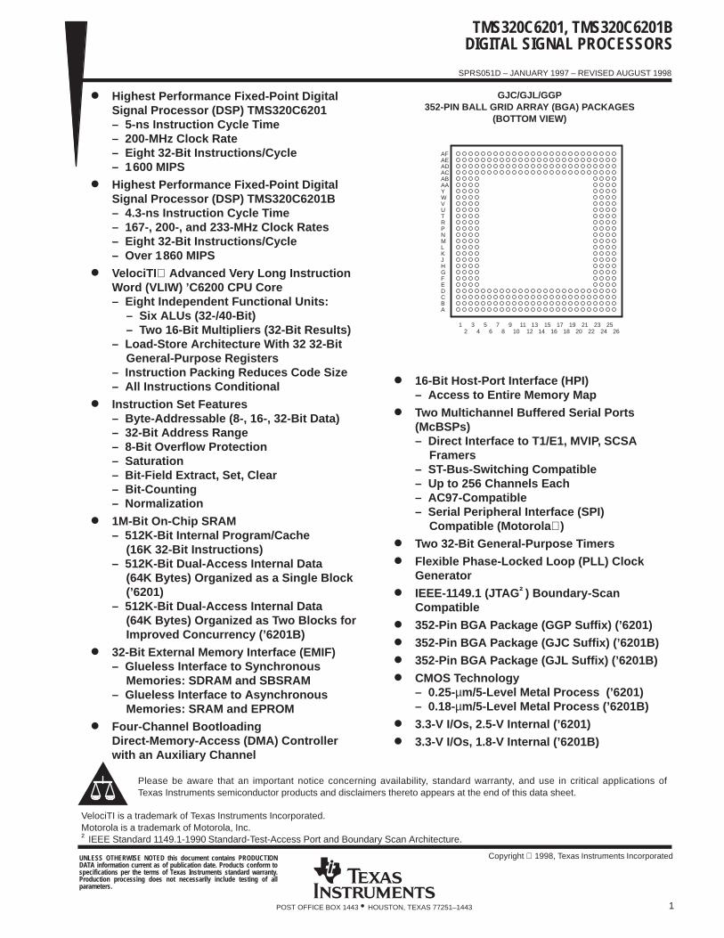
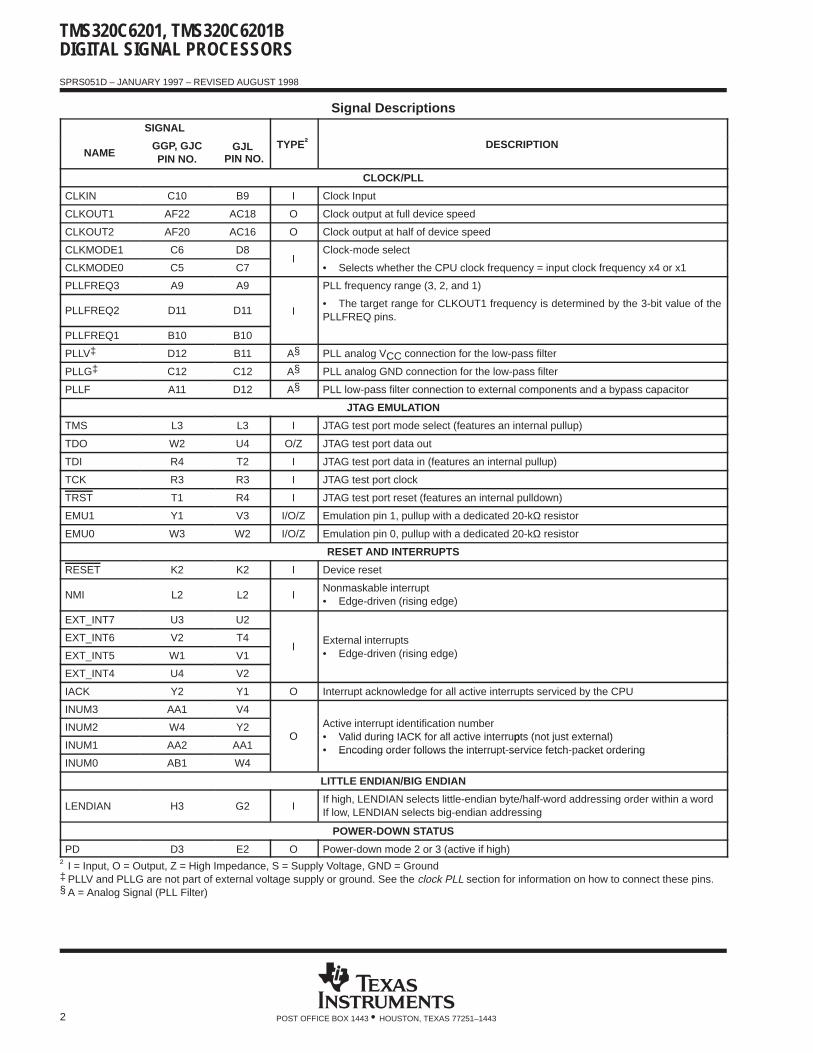
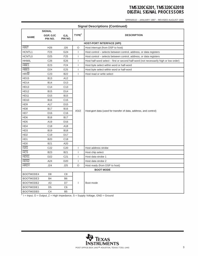
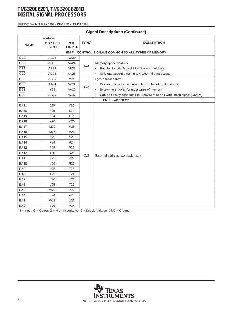
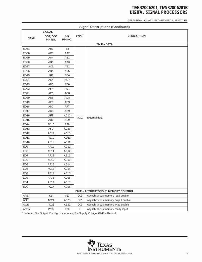

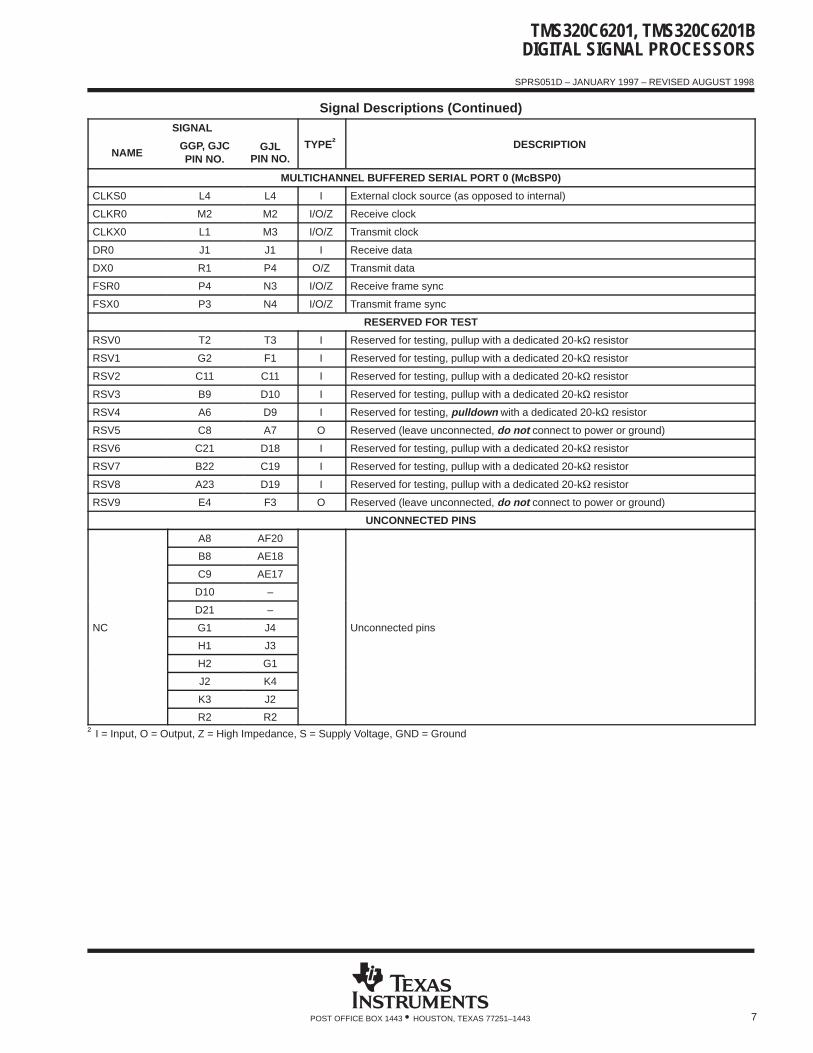
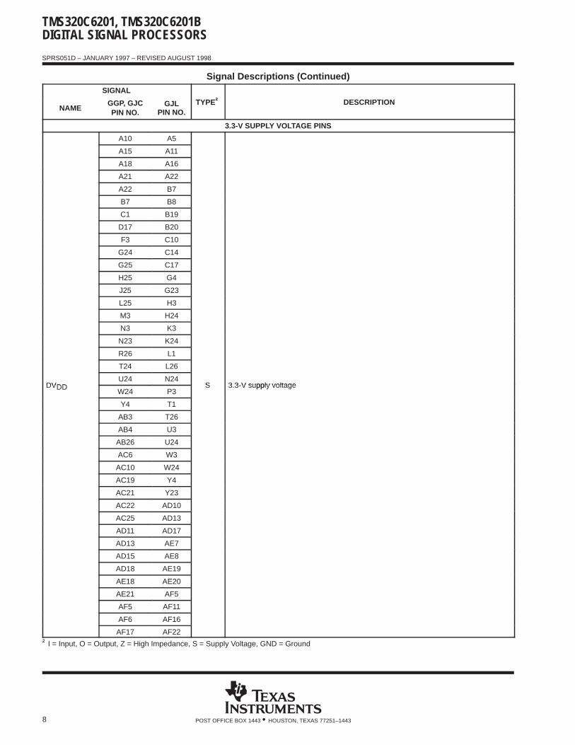

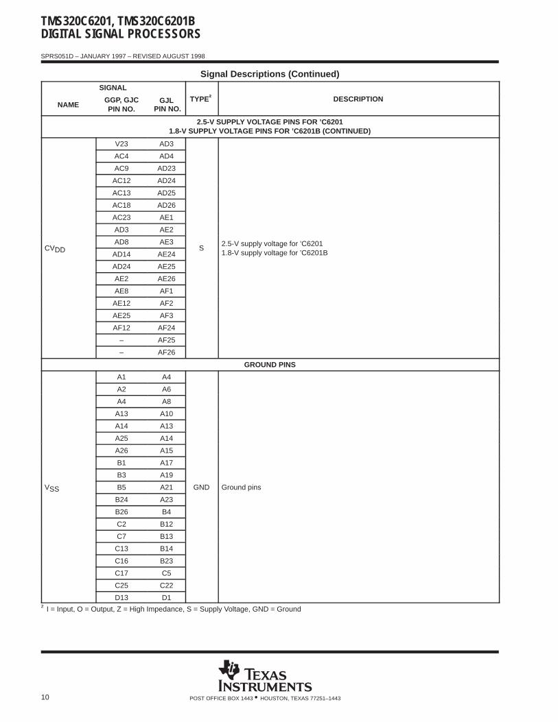
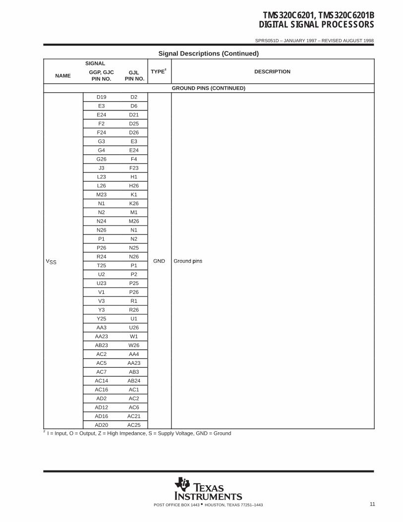
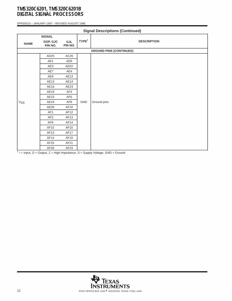

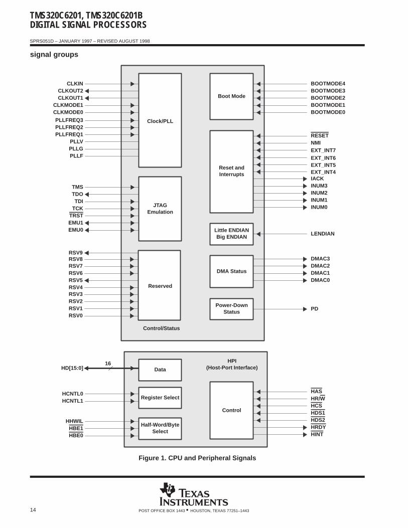

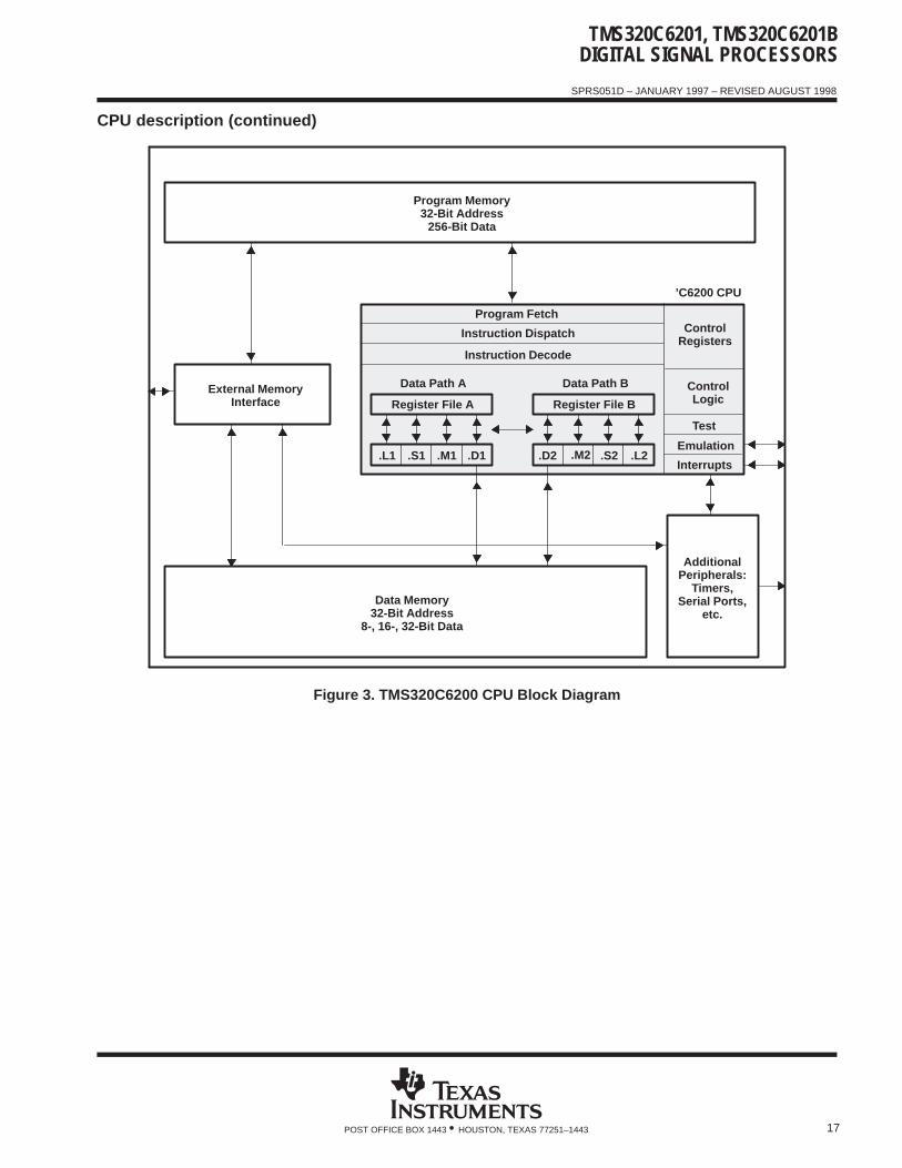
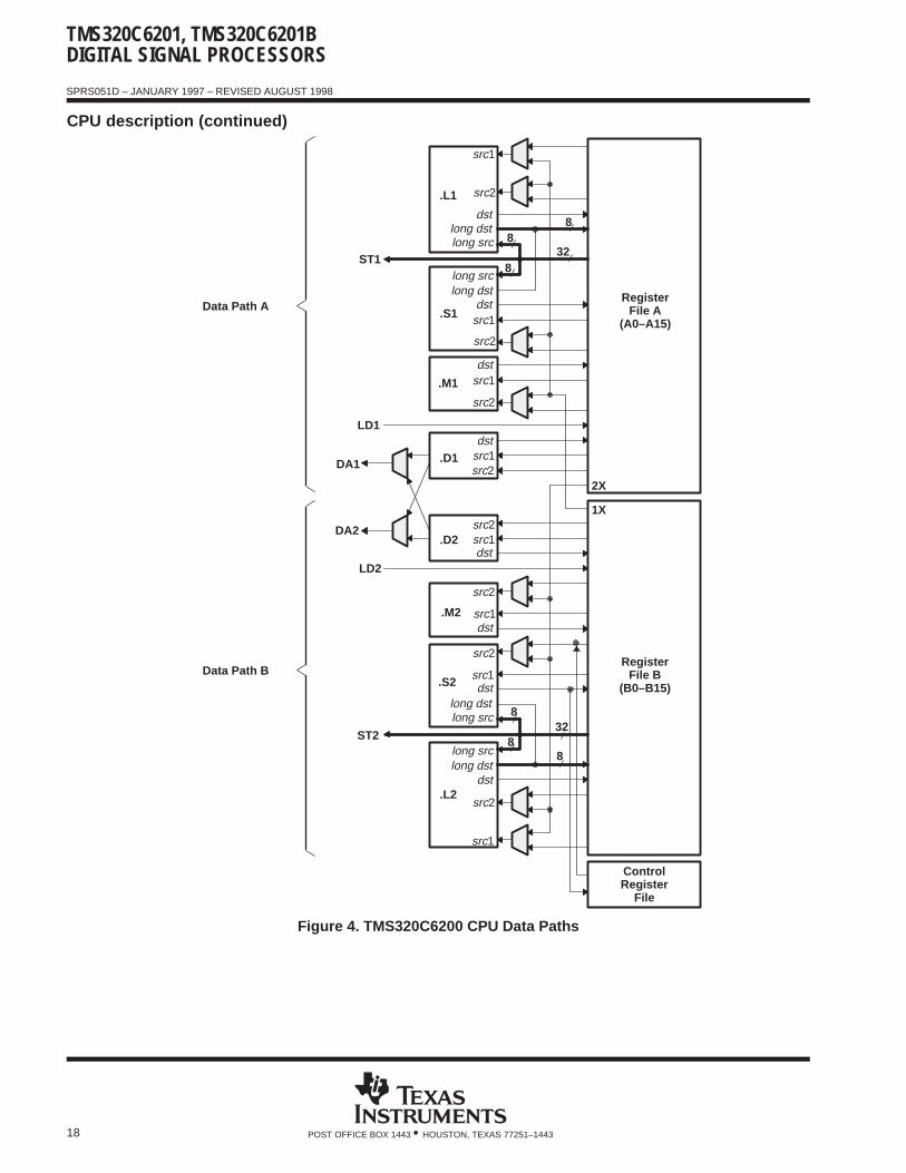
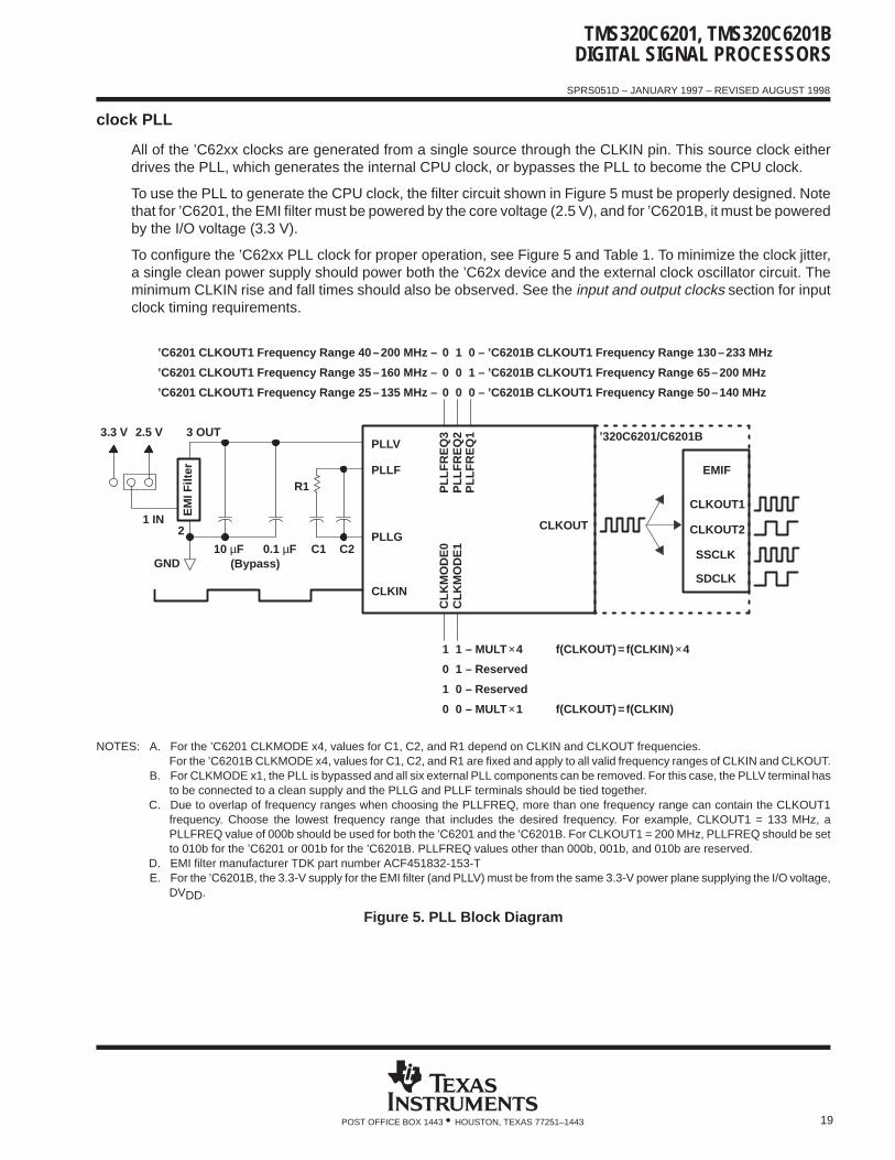

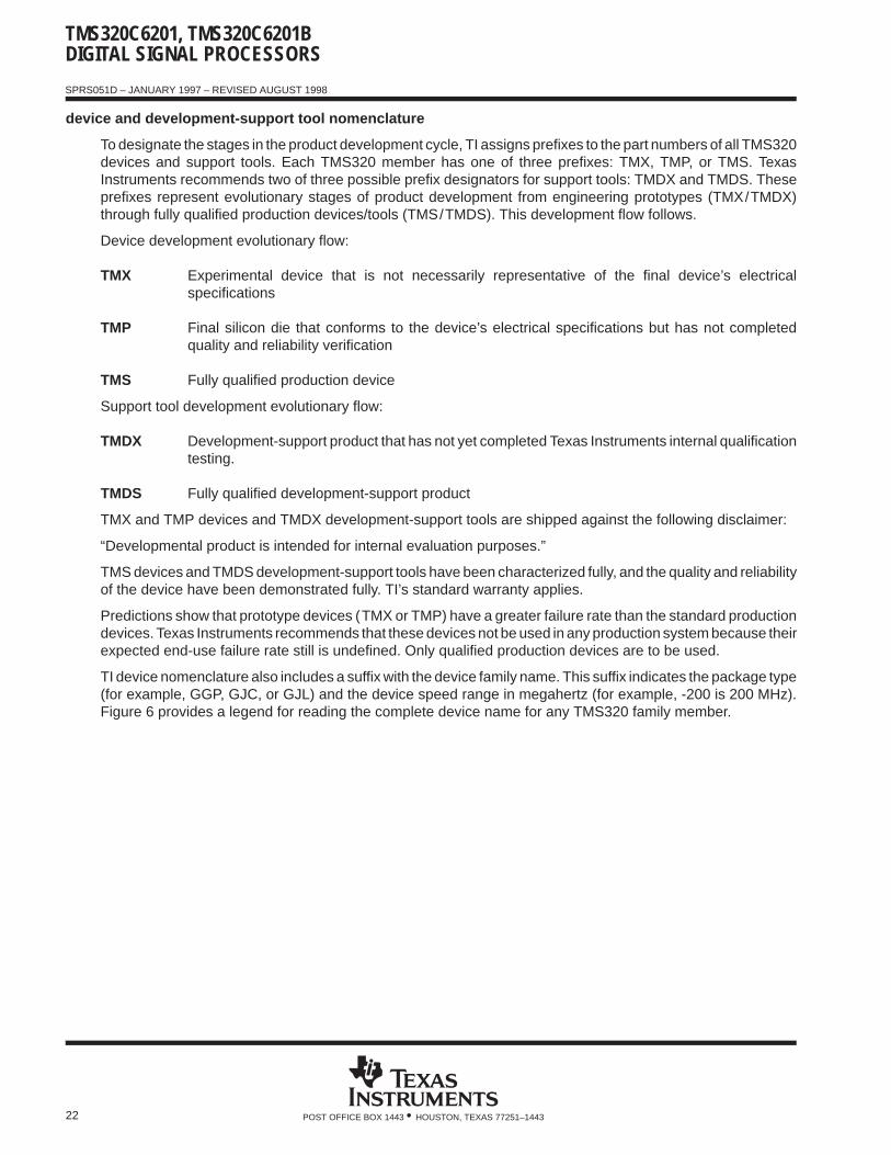
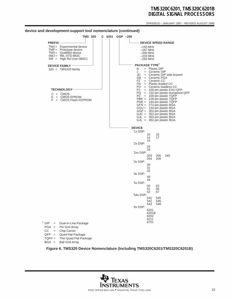
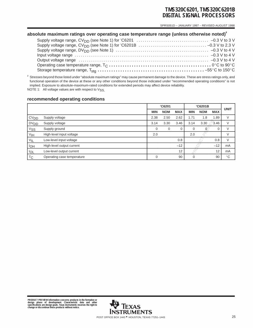
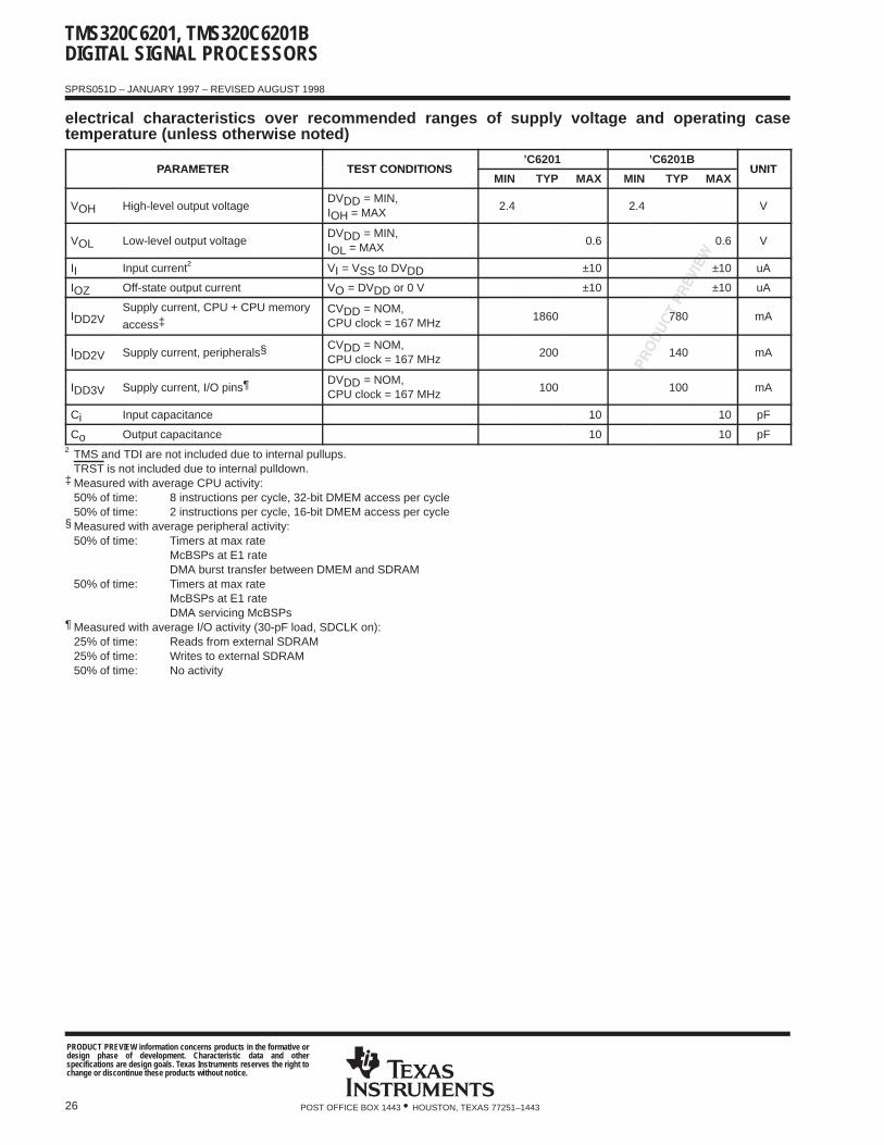
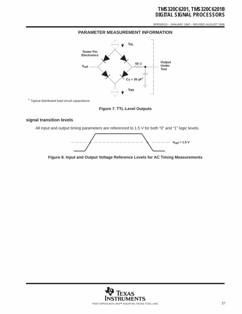
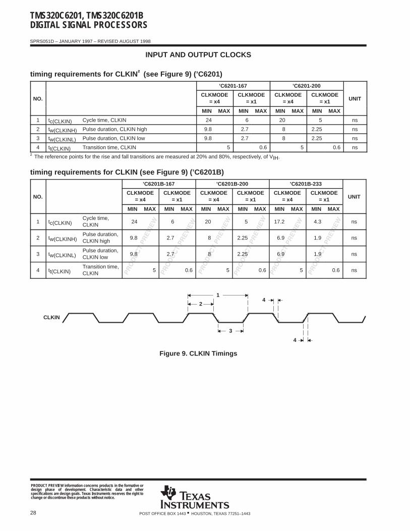

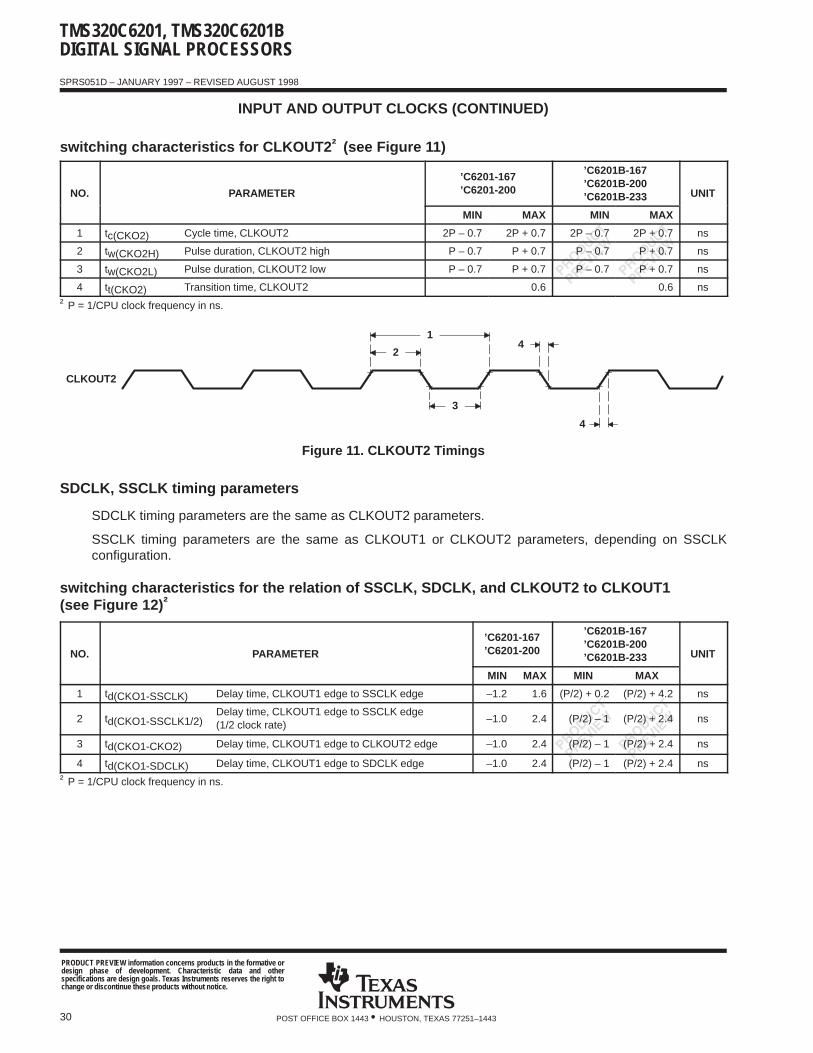

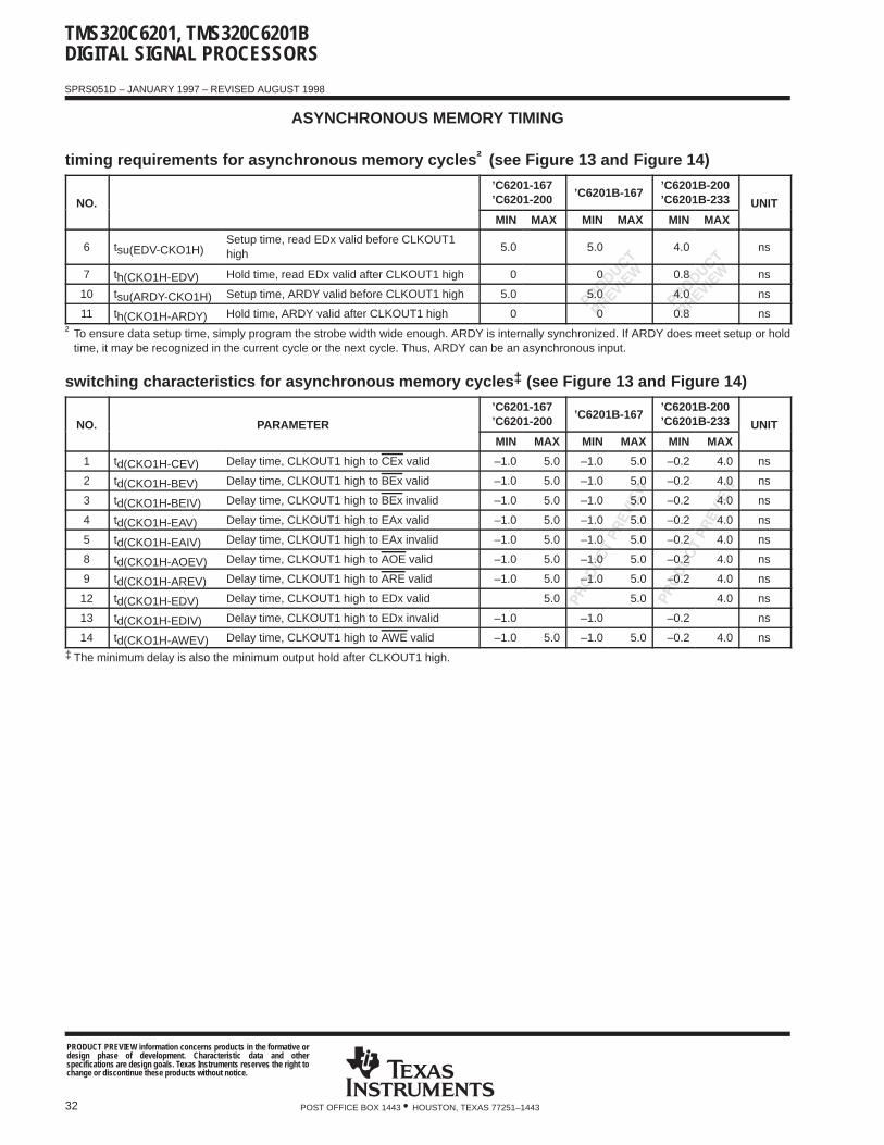
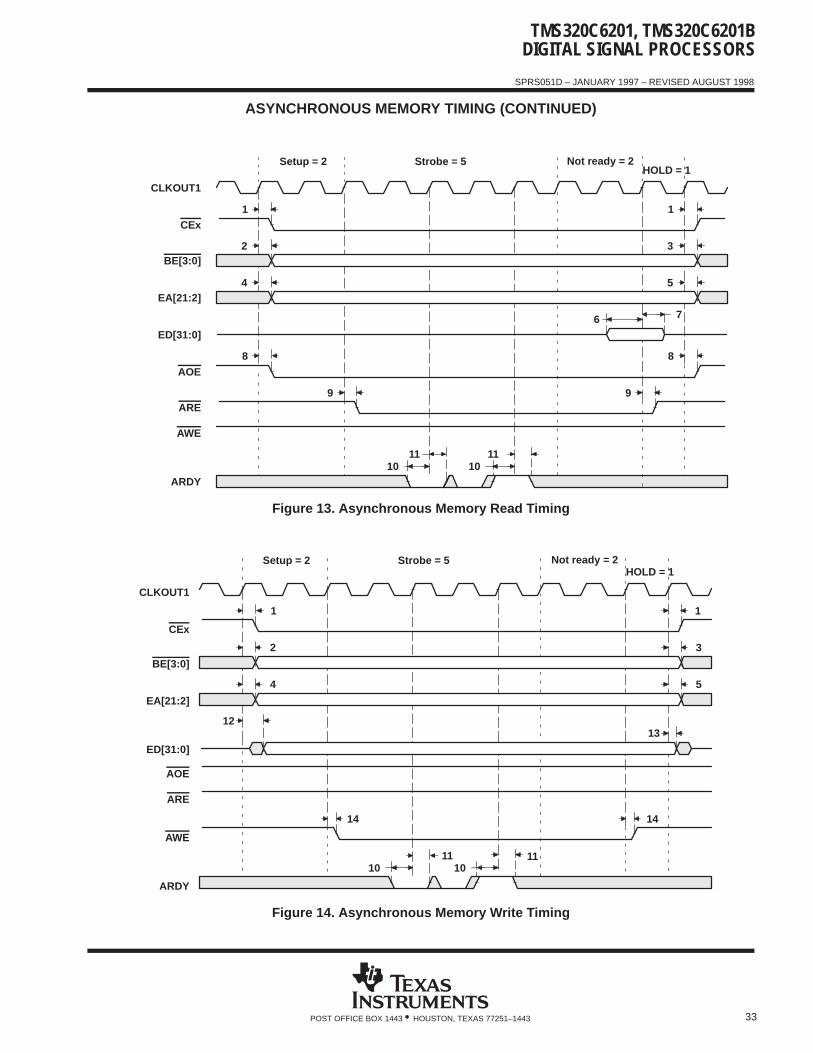
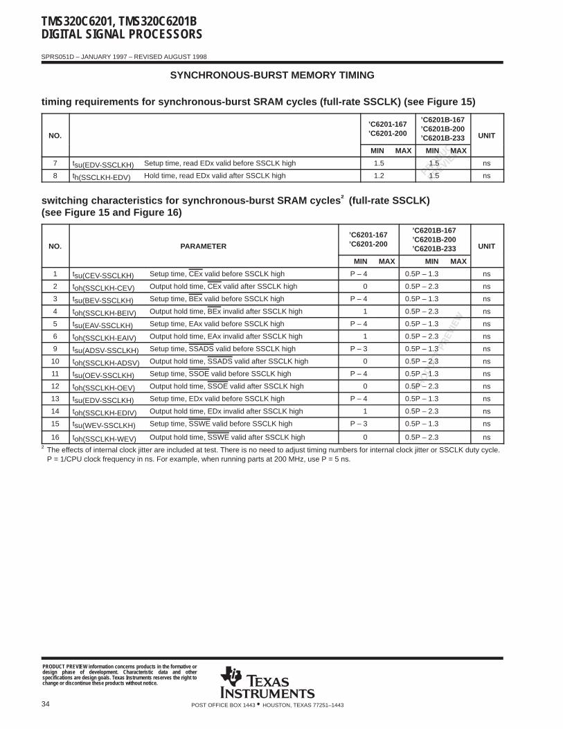
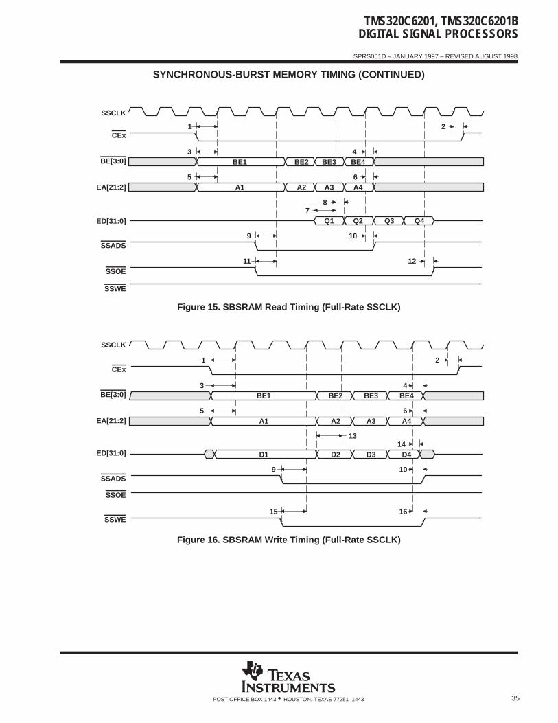
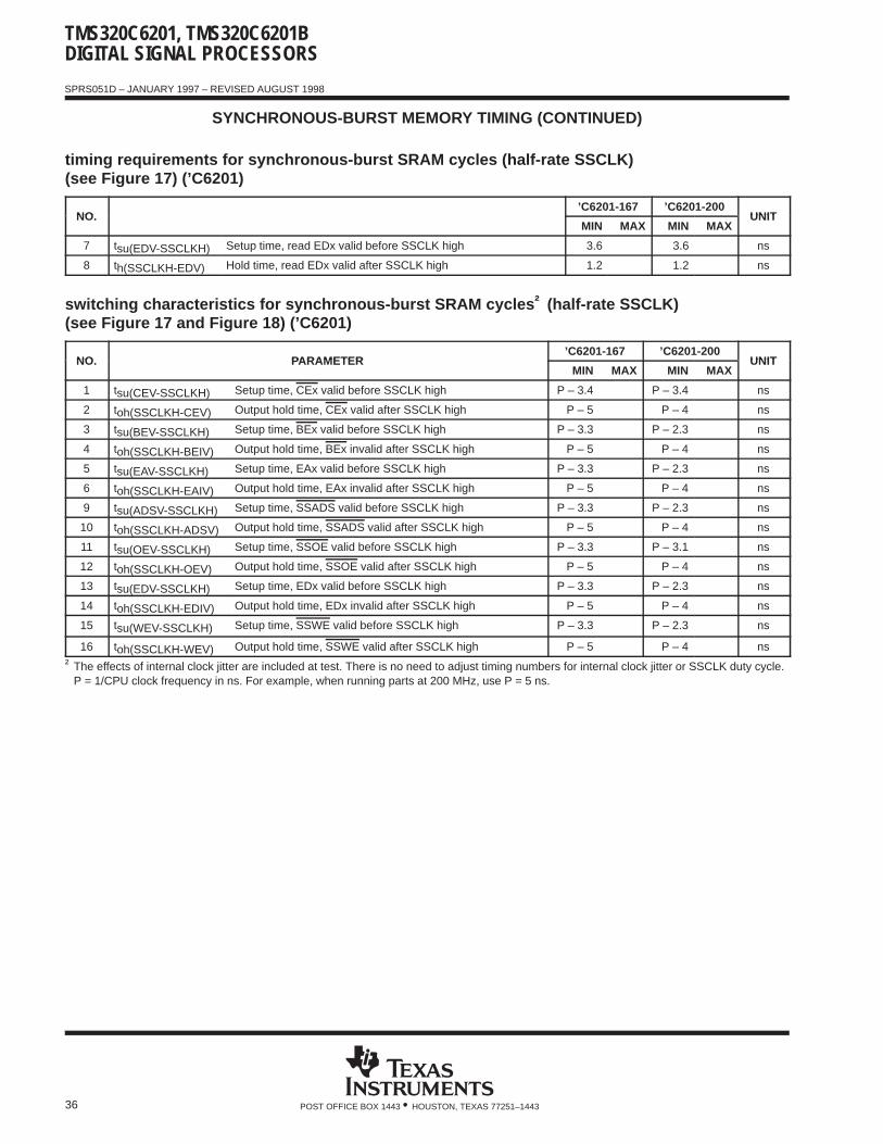
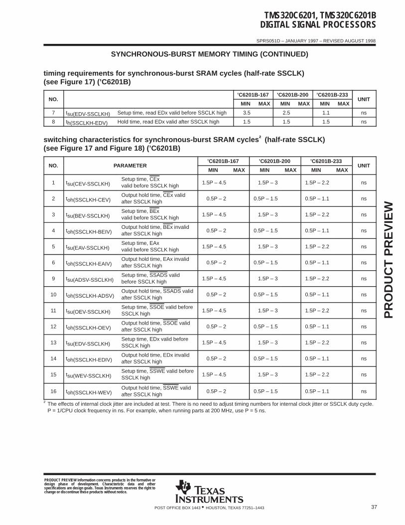
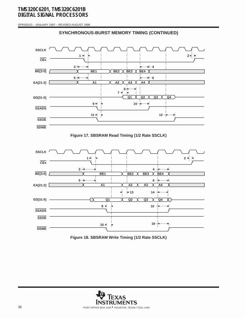
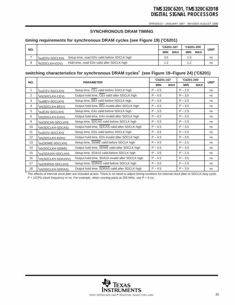
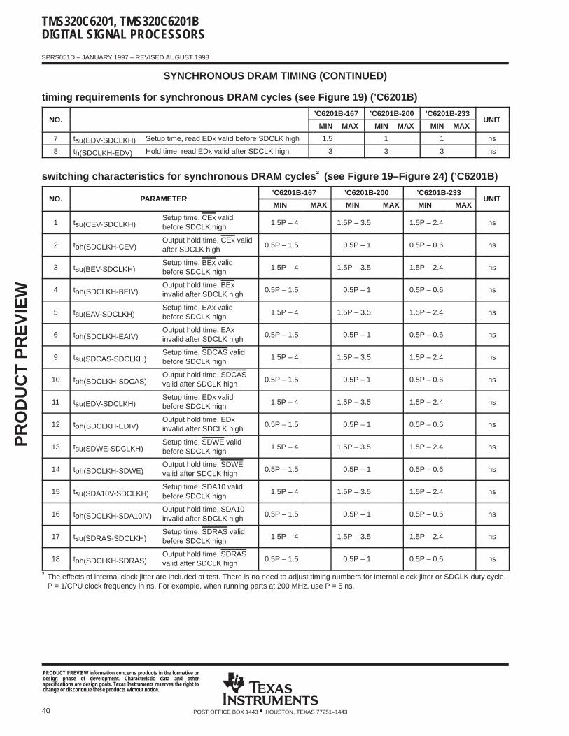
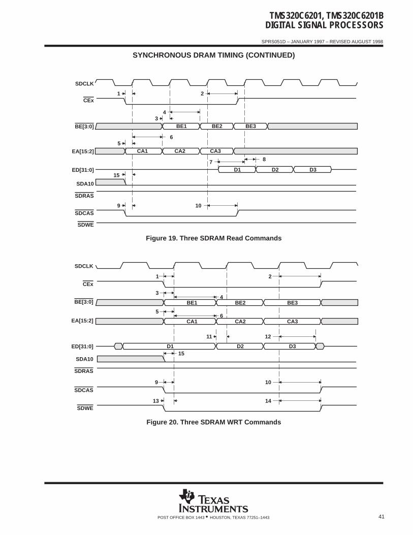
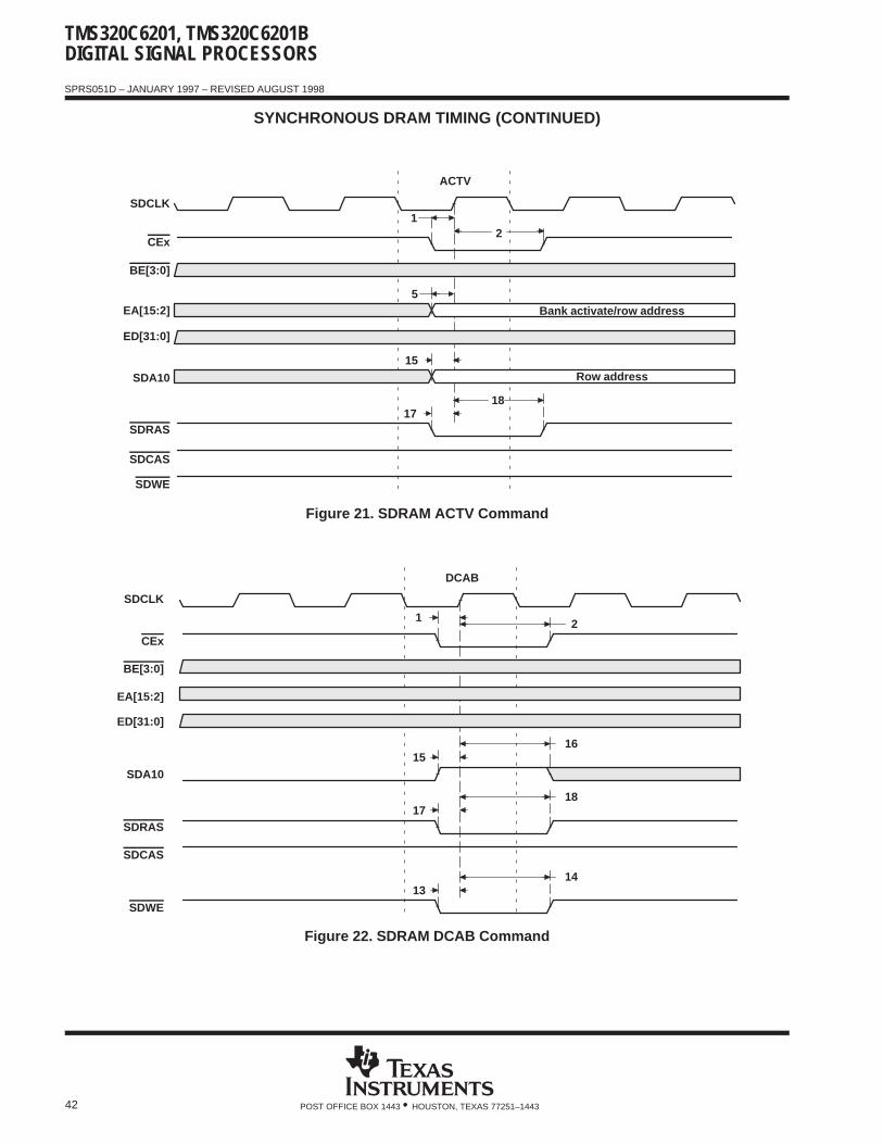
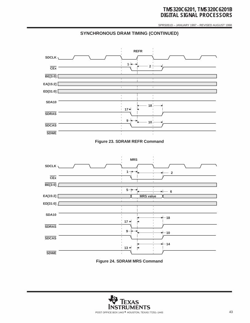
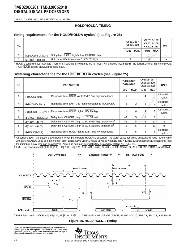
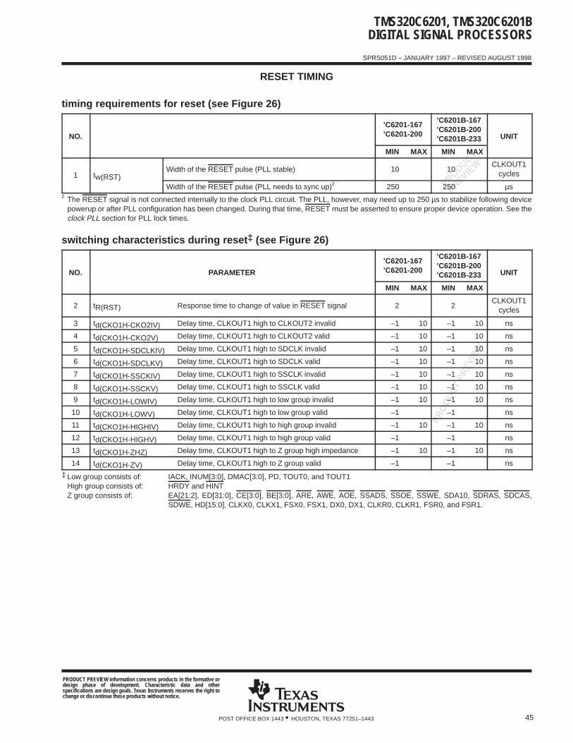

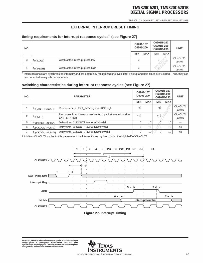
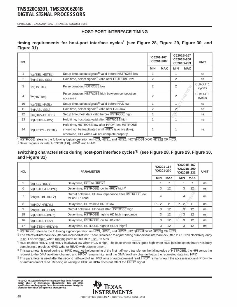

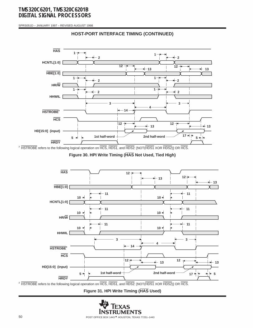
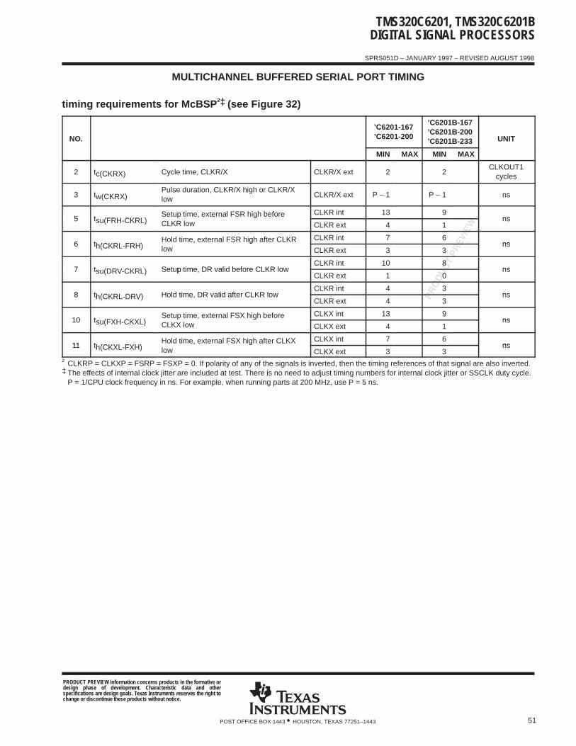
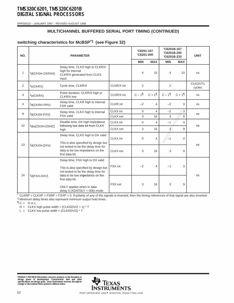
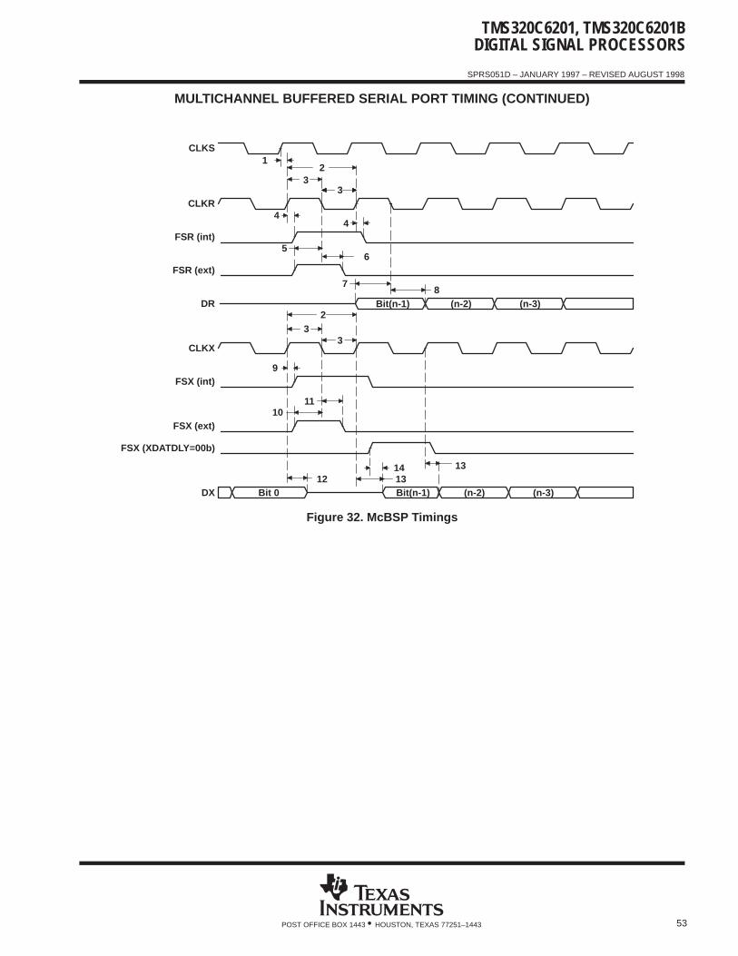
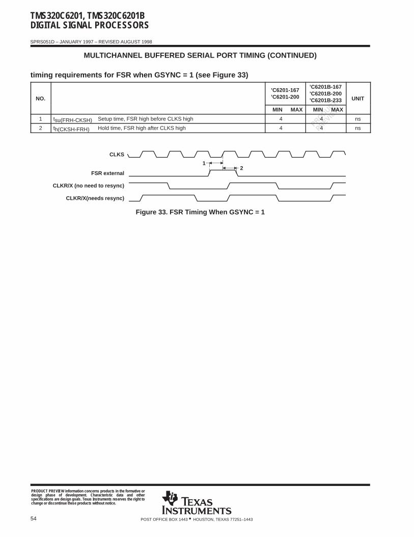
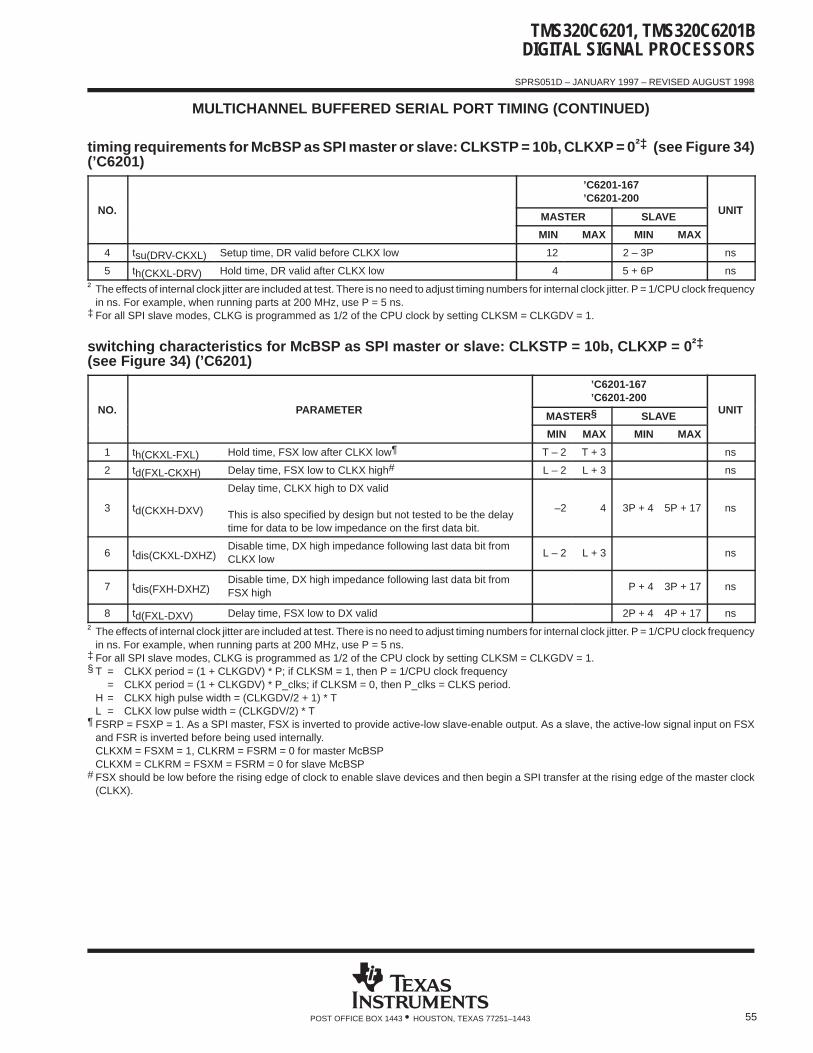
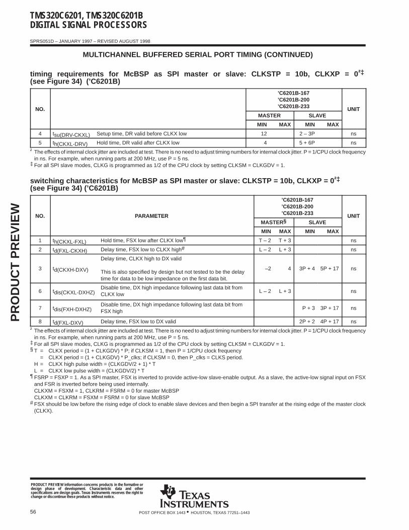
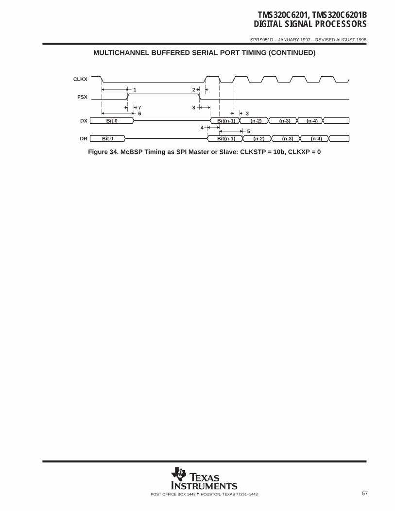
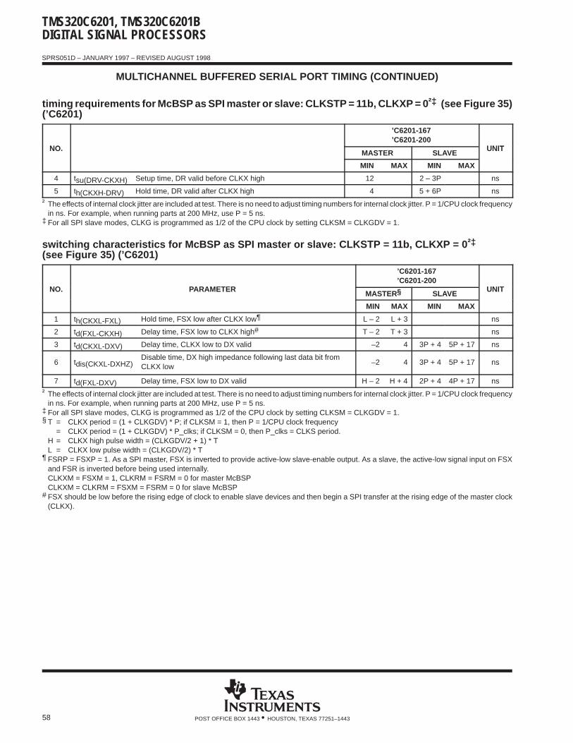
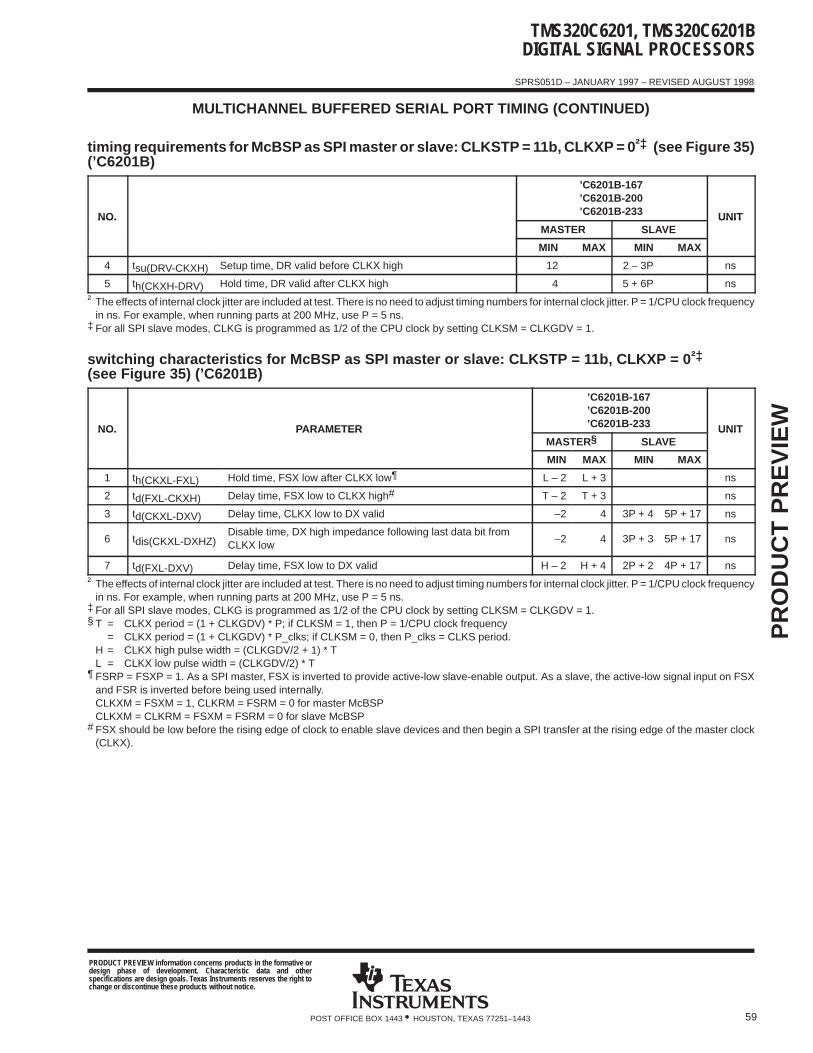
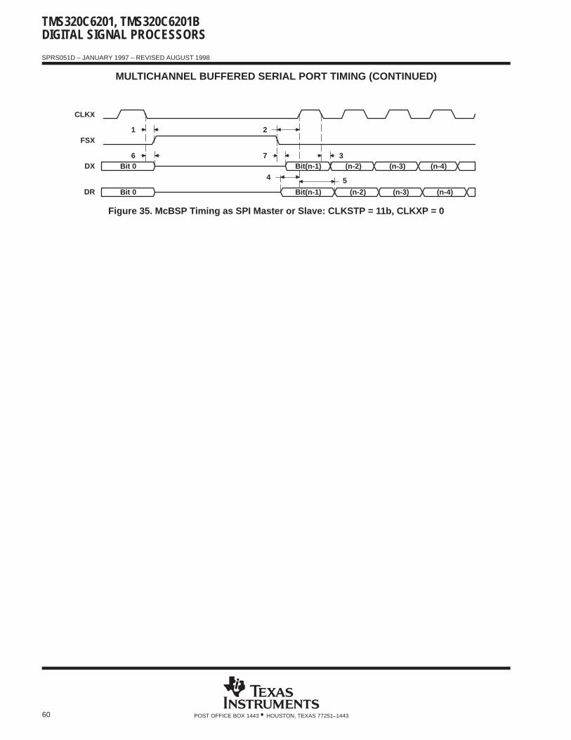


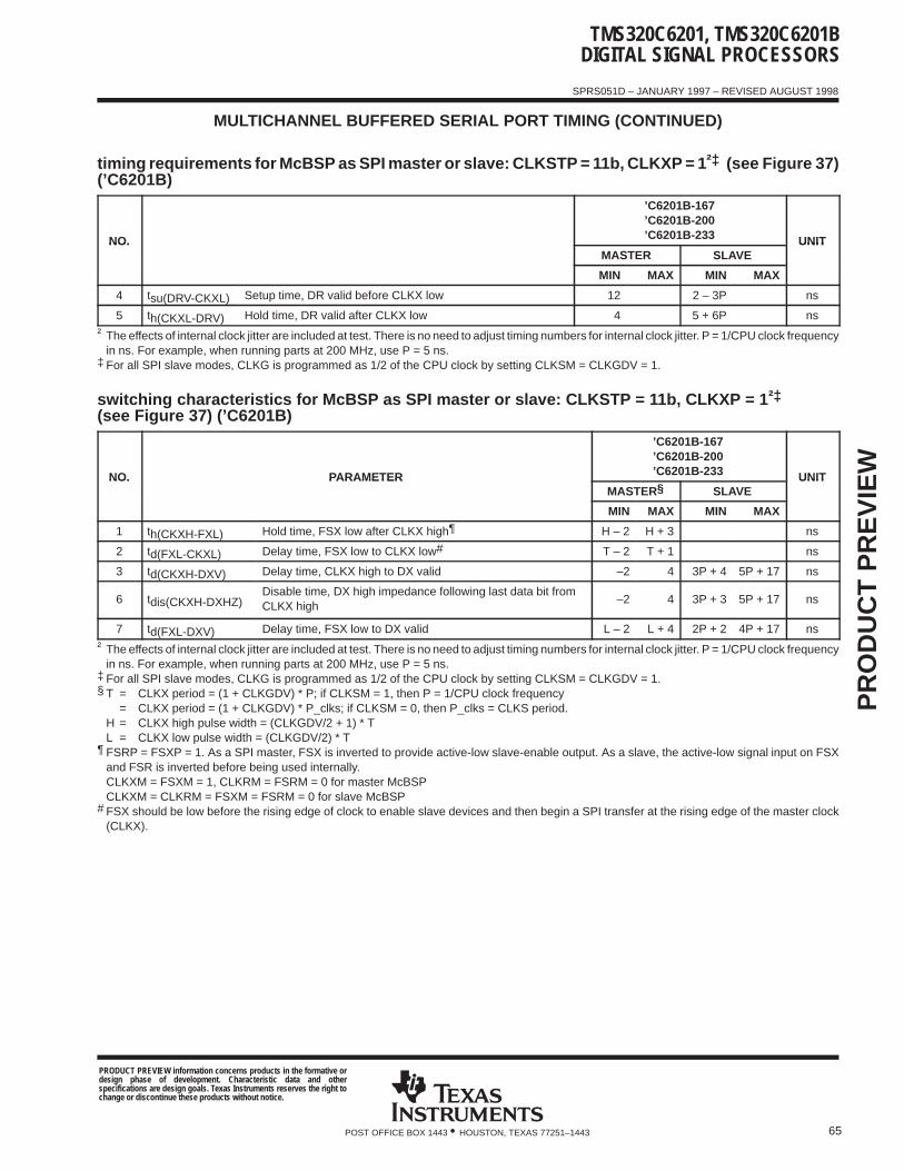

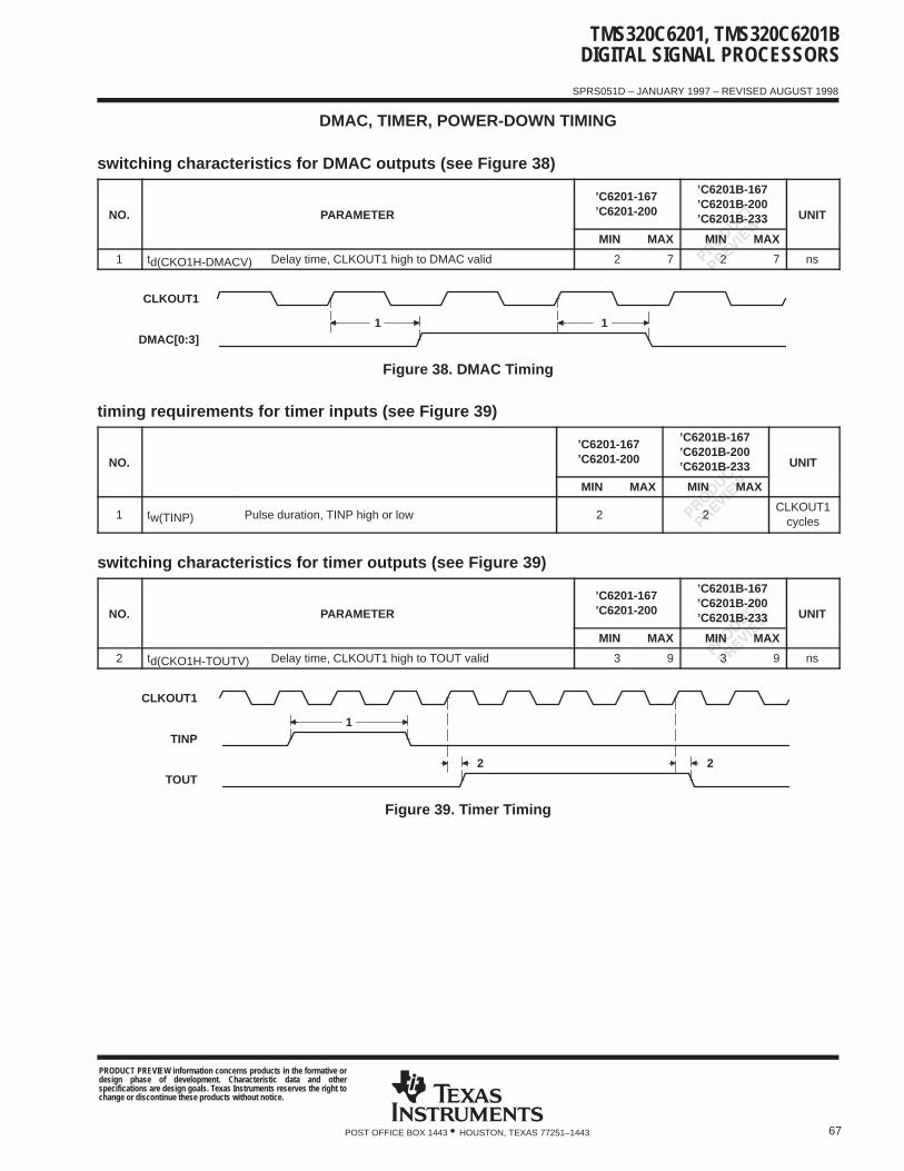
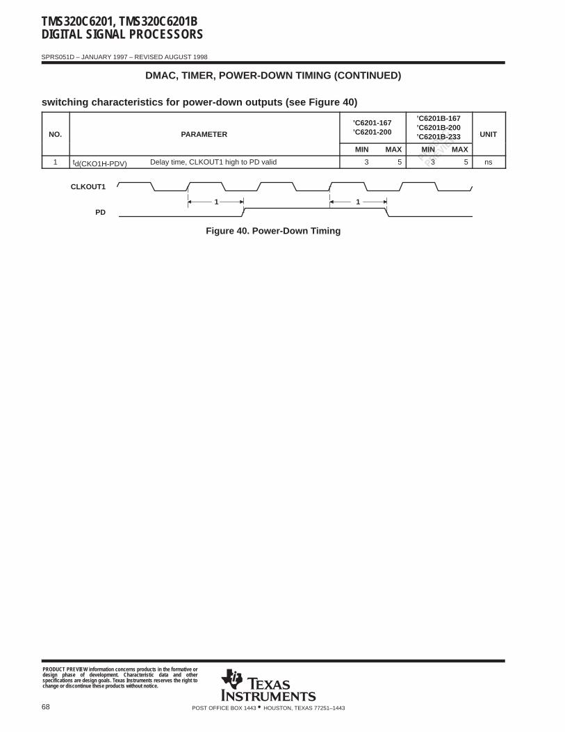
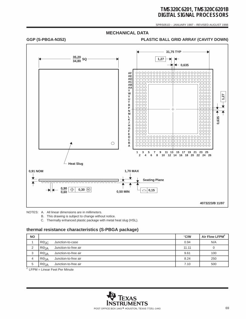
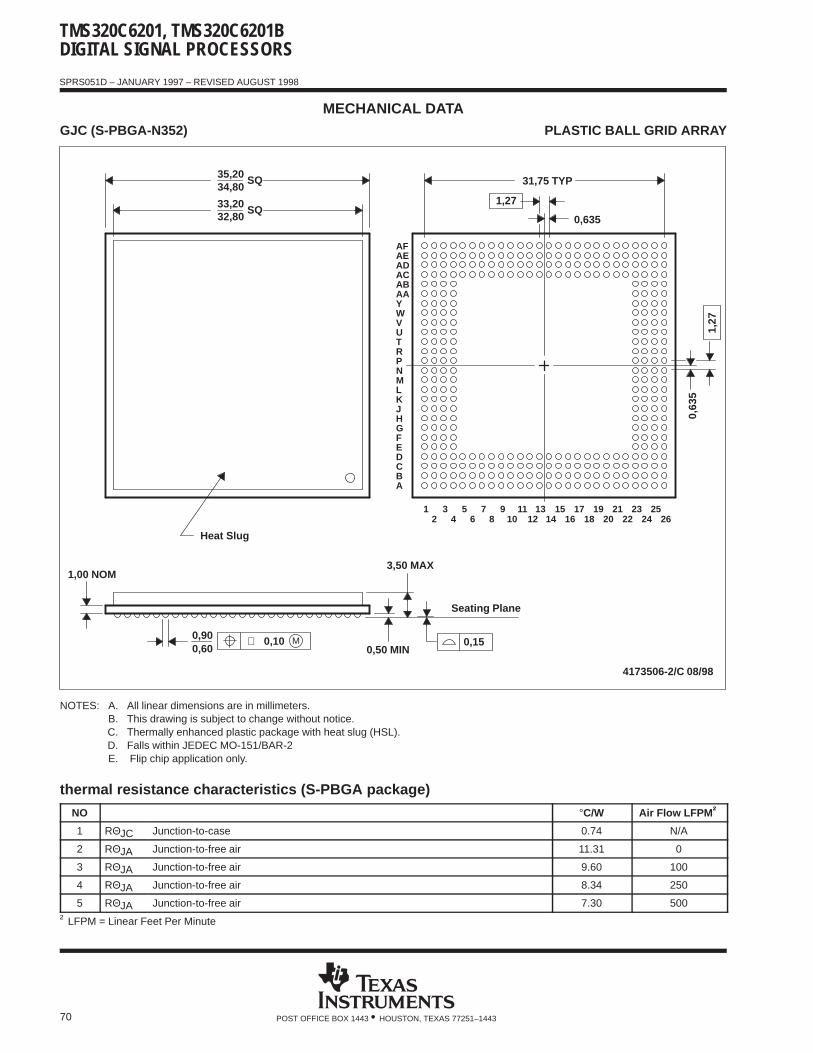
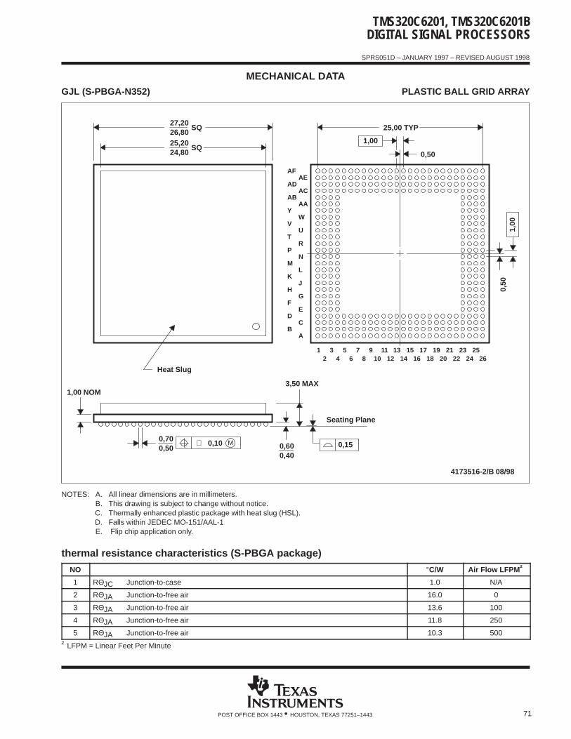


![TMS320x28xx Digital Signal Processors-[DM]-[SPRS174]](https://static.documents.pub/doc/80x56/54a12fc6ac7959c87d8b4690/tms320x28xx-digital-signal-processors-dm-sprs174.jpg)

