285
TMS320VC5501/5502/5503/5507/5509/5510 DSP Multichannel Buffered Serial Port (McBSP) Reference Guide Literature Number: SPRU592E April 2005

TMS320VC5501/5502/5503/5507/5509/5510 DSPMultichannel Buffered Serial Port (McBSP)
Reference Guide
Literature Number: SPRU592EApril 2005

iiiRead This First
Preface
Read This First
About This Manual
This manual describes the type of multichannel buffered serial ports (McBSP)available on the TMS320C55x™ DSPs. The McBSPs provide a direct serialinterface between a C55x™ DSP and other devices in a system. For thenumber of McBSPs available on a particular C55x device, see thedevice-specific data manual.
Notational Conventions
This document uses the following conventions.
� When the part number TMS320VC5509 is used, it refers both toTMS320VC5509 devices and to TMS320VC5509A devices.
� In most cases, hexadecimal numbers are shown with the suffix h. Forexample, the following number is a hexadecimal 40 (decimal 64):
40h
Similarly, binary numbers often are shown with the suffix b. For example,the following number is the decimal number 4 shown in binary form:
0100b
� If a signal or pin is active low, it has an overbar. For example, the RESETsignal is active low.
Related Documentation From Texas Instruments
The following documents describe the C55x devices and related support tools.Copies of these documents are available on the Internet at www.ti.com.Tip: Enter the literature number in the search box provided at www.ti.com.
TMS320VC5501 Fixed-Point Digital Signal Processor Data Manual(literature number SPRS206) describes the features of theTMS320VC5501 fixed-point DSP and provides signal descriptions,pinouts, electrical specifications, and timings for the device.

Related Documentation From Texas Instruments
iv
TMS320VC5502 Fixed-Point Digital Signal Processor Data Manual(literature number SPRS166) describes the features of theTMS320VC5502 fixed-point DSP and provides signal descriptions,pinouts, electrical specifications, and timings for the device.
TMS320VC5503 Fixed-Point Digital Signal Processor Data Manual (litera-ture number SPRS245) describes the features of the TMS320VC5503fixed-point DSP and provides signal descriptions, pinouts, electricalspecifications, and timings for the device.
TMS320VC5507 Fixed-Point Digital Signal Processor Data Manual (litera-ture number SPRS244) describes the features of the TMS320VC5507fixed-point DSP and provides signal descriptions, pinouts, electricalspecifications, and timings for the device.
TMS320VC5509 Fixed-Point Digital Signal Processor Data Manual(literature number SPRS163) describes the features of theTMS320VC5509 fixed-point DSP and provides signal descriptions,pinouts, electrical specifications, and timings for the device.
TMS320VC5509A Fixed-Point Digital Signal Processor Data Manual(literature number SPRS205) describes the features of theTMS320VC5509A fixed-point DSP and provides signal descriptions,pinouts, electrical specifications, and timings for the device.
TMS320VC5510 Fixed-Point Digital Signal Processor Data Manual(literature number SPRS076) describes the features of theTMS320VC5510 fixed-point DSP and provides signal descriptions,pinouts, electrical specifications, and timings for the device.
TMS320C55x Technical Overview (literature number SPRU393) introducesthe TMS320C55x DSPs, the latest generation of fixed-point DSPs in theTMS320C5000™ DSP platform. Like the previous generations, thisprocessor is optimized for high performance and low-power operation.This book describes the CPU architecture, low-power enhancements,and embedded emulation features.
TMS320C55x DSP CPU Reference Guide (literature number SPRU371)describes the architecture, registers, and operation of the CPU for theTMS320C55x DSPs.
TMS320C55x DSP Peripherals Overview Reference Guide (literaturenumber SPRU317) introduces the peripherals, interfaces, and relatedhardware that are available on TMS320C55x DSPs.

Related Documentation From Texas Instruments
vRead This First
TMS320C55x DSP Algebraic Instruction Set Reference Guide (literaturenumber SPRU375) describes the TMS320C55x DSP algebraicinstructions individually. Also includes a summary of the instruction set,a list of the instruction opcodes, and a cross-reference to the mnemonicinstruction set.
TMS320C55x DSP Mnemonic Instruction Set Reference Guide (literaturenumber SPRU374) describes the TMS320C55x DSP mnemonicinstructions individually. Also includes a summary of the instruction set,a list of the instruction opcodes, and a cross-reference to the algebraicinstruction set.
TMS320C55x Optimizing C/C++ Compiler User’s Guide (literature numberSPRU281) describes the TMS320C55x C/C++ Compiler. This C/C++compiler accepts ISO standard C and C++ source code and producesassembly language source code for TMS320C55x devices.
TMS320C55x Assembly Language Tools User’s Guide (literature numberSPRU280) describes the assembly language tools (assembler, linker,and other tools used to develop assembly language code), assemblerdirectives, macros, common object file format, and symbolic debuggingdirectives for TMS320C55x devices.
TMS320C55x DSP Programmer’s Guide (literature number SPRU376)describes ways to optimize C and assembly code for the TMS320C55xDSPs and explains how to write code that uses special features andinstructions of the DSPs.
Trademarks
TMS320C5000, TMS320C55x, and C55x are trademarks ofTexas Instruments.
Other trademarks are the property of their respective owners.
Related Documentation From Texas Instruments / Trademarks

vi
This page is intentionally left blank.

Contents
vii
Contents
1 Introduction to the McBSP 1-1. . . . . . . . . . . . . . . . . . . . . . . . . . . . . . . . . . . . . . . . . . . . . . . . . . . . . . . 1.1 Introduction 1-2. . . . . . . . . . . . . . . . . . . . . . . . . . . . . . . . . . . . . . . . . . . . . . . . . . . . . . . . . . . . . . . . 1.2 Key Features of the McBSP 1-2. . . . . . . . . . . . . . . . . . . . . . . . . . . . . . . . . . . . . . . . . . . . . . . . . . 1.3 Block Diagram of the McBSP 1-4. . . . . . . . . . . . . . . . . . . . . . . . . . . . . . . . . . . . . . . . . . . . . . . . . 1.4 McBSP Pins 1-6. . . . . . . . . . . . . . . . . . . . . . . . . . . . . . . . . . . . . . . . . . . . . . . . . . . . . . . . . . . . . . .
2 McBSP Operation 2-1. . . . . . . . . . . . . . . . . . . . . . . . . . . . . . . . . . . . . . . . . . . . . . . . . . . . . . . . . . . . . . . . 2.1 Data Transfer Process of a McBSP 2-2. . . . . . . . . . . . . . . . . . . . . . . . . . . . . . . . . . . . . . . . . . .
2.1.1 Data Transfer Process for Word Length of 8, 12, or 16 Bits 2-2. . . . . . . . . . . . . . . . 2.1.2 Data Transfer Process for Word Length of 20, 24, or 32 Bits 2-3. . . . . . . . . . . . . .
2.2 Companding (Compressing and Expanding) Data 2-4. . . . . . . . . . . . . . . . . . . . . . . . . . . . . . . 2.2.1 Companding Formats 2-4. . . . . . . . . . . . . . . . . . . . . . . . . . . . . . . . . . . . . . . . . . . . . . . . 2.2.2 Capability to Compand Internal Data 2-5. . . . . . . . . . . . . . . . . . . . . . . . . . . . . . . . . . . 2.2.3 Reversing Bit Order: Option to Transfer LSB First 2-6. . . . . . . . . . . . . . . . . . . . . . . .
2.3 Clocking and Framing Data 2-7. . . . . . . . . . . . . . . . . . . . . . . . . . . . . . . . . . . . . . . . . . . . . . . . . . 2.3.1 Clocking 2-7. . . . . . . . . . . . . . . . . . . . . . . . . . . . . . . . . . . . . . . . . . . . . . . . . . . . . . . . . . . . 2.3.2 Serial Words 2-7. . . . . . . . . . . . . . . . . . . . . . . . . . . . . . . . . . . . . . . . . . . . . . . . . . . . . . . . 2.3.3 Frames and Frame Synchronization 2-8. . . . . . . . . . . . . . . . . . . . . . . . . . . . . . . . . . . 2.3.4 Detecting Frame-Sync Pulses, Even in the Reset State 2-9. . . . . . . . . . . . . . . . . . . 2.3.5 Ignoring Unexpected Frame-Sync Pulses 2-9. . . . . . . . . . . . . . . . . . . . . . . . . . . . . . . 2.3.6 Frame Frequency 2-9. . . . . . . . . . . . . . . . . . . . . . . . . . . . . . . . . . . . . . . . . . . . . . . . . . . 2.3.7 Maximum Frame Frequency 2-9. . . . . . . . . . . . . . . . . . . . . . . . . . . . . . . . . . . . . . . . . .
2.4 Frame Phases 2-11. . . . . . . . . . . . . . . . . . . . . . . . . . . . . . . . . . . . . . . . . . . . . . . . . . . . . . . . . . . . 2.4.1 Number of Phases, Words, and Bits Per Frame 2-11. . . . . . . . . . . . . . . . . . . . . . . . 2.4.2 Single-Phase Frame Example 2-11. . . . . . . . . . . . . . . . . . . . . . . . . . . . . . . . . . . . . . . . 2.4.3 Dual-Phase Frame Example 2-12. . . . . . . . . . . . . . . . . . . . . . . . . . . . . . . . . . . . . . . . . 2.4.4 Implementing the AC97 Standard With a Dual-Phase Frame 2-13. . . . . . . . . . . . .
2.5 McBSP Reception 2-15. . . . . . . . . . . . . . . . . . . . . . . . . . . . . . . . . . . . . . . . . . . . . . . . . . . . . . . . . 2.6 McBSP Transmission 2-17. . . . . . . . . . . . . . . . . . . . . . . . . . . . . . . . . . . . . . . . . . . . . . . . . . . . . . 2.7 Interrupts and DMA Events Generated by a McBSP 2-19. . . . . . . . . . . . . . . . . . . . . . . . . . . .
3 Sample Rate Generator of the McBSP 3-1. . . . . . . . . . . . . . . . . . . . . . . . . . . . . . . . . . . . . . . . . . . . . 3.1 Sample Rate Generator 3-2. . . . . . . . . . . . . . . . . . . . . . . . . . . . . . . . . . . . . . . . . . . . . . . . . . . . . 3.2 Clock Generation in the Sample Rate Generator 3-4. . . . . . . . . . . . . . . . . . . . . . . . . . . . . . . .
3.2.1 Choosing an Input Clock 3-5. . . . . . . . . . . . . . . . . . . . . . . . . . . . . . . . . . . . . . . . . . . . . 3.2.2 Choosing a Polarity for the Input Clock 3-6. . . . . . . . . . . . . . . . . . . . . . . . . . . . . . . . .

Contents
viii
3.2.3 Choosing a Frequency for the Output Clock (CLKG) 3-7. . . . . . . . . . . . . . . . . . . . . 3.2.4 Keeping CLKG Synchronized to an External Input Clock 3-8. . . . . . . . . . . . . . . . . .
3.3 Frame Sync Generation in the Sample Rate Generator 3-9. . . . . . . . . . . . . . . . . . . . . . . . . . 3.3.1 Choosing the Width of the Frame-Sync Pulse on FSG 3-9. . . . . . . . . . . . . . . . . . . . 3.3.2 Controlling the Period Between the Starting Edges of Frame-Sync Pulses on . . .
FSG 3-9. . . . . . . . . . . . . . . . . . . . . . . . . . . . . . . . . . . . . . . . . . . . . . . . . . . . . . . . . . . . . . . 3.4 Synchronizing Sample Rate Generator Outputs to an External Clock 3-10. . . . . . . . . . . . .
3.4.1 Synchronization Examples 3-10. . . . . . . . . . . . . . . . . . . . . . . . . . . . . . . . . . . . . . . . . . . 3.5 Reset and Initialization Procedure for the Sample Rate Generator 3-12. . . . . . . . . . . . . . . . 3.6 Sample Rate Generator Clocking Examples 3-14. . . . . . . . . . . . . . . . . . . . . . . . . . . . . . . . . . .
3.6.1 Double-Rate ST-Bus Clock 3-14. . . . . . . . . . . . . . . . . . . . . . . . . . . . . . . . . . . . . . . . . . 3.6.2 Single-Rate ST-Bus Clock 3-15. . . . . . . . . . . . . . . . . . . . . . . . . . . . . . . . . . . . . . . . . . . 3.6.3 Other Double-Rate Clock 3-16. . . . . . . . . . . . . . . . . . . . . . . . . . . . . . . . . . . . . . . . . . . .
4 McBSP Exception/Error Conditions 4-1. . . . . . . . . . . . . . . . . . . . . . . . . . . . . . . . . . . . . . . . . . . . . . . 4.1 McBSP Exception/Error Conditions 4-2. . . . . . . . . . . . . . . . . . . . . . . . . . . . . . . . . . . . . . . . . . . 4.2 Overrun in the Receiver 4-3. . . . . . . . . . . . . . . . . . . . . . . . . . . . . . . . . . . . . . . . . . . . . . . . . . . . .
4.2.1 Example of the Overrun Condition 4-3. . . . . . . . . . . . . . . . . . . . . . . . . . . . . . . . . . . . . 4.2.2 Example of Preventing the Overrun Condition 4-4. . . . . . . . . . . . . . . . . . . . . . . . . . .
4.3 Unexpected Receive Frame-Sync Pulse 4-5. . . . . . . . . . . . . . . . . . . . . . . . . . . . . . . . . . . . . . . 4.3.1 Possible Responses to Receive Frame-Sync Pulses 4-5. . . . . . . . . . . . . . . . . . . . . 4.3.2 Example of an Unexpected Receive Frame-Sync Pulse 4-6. . . . . . . . . . . . . . . . . . 4.3.3 Preventing Unexpected Receive Frame-Sync Pulses 4-7. . . . . . . . . . . . . . . . . . . . .
4.4 Overwrite in the Transmitter 4-8. . . . . . . . . . . . . . . . . . . . . . . . . . . . . . . . . . . . . . . . . . . . . . . . . . 4.4.1 Example of the Overwrite Condition 4-8. . . . . . . . . . . . . . . . . . . . . . . . . . . . . . . . . . . . 4.4.2 Preventing Overwrites 4-8. . . . . . . . . . . . . . . . . . . . . . . . . . . . . . . . . . . . . . . . . . . . . . . .
4.5 Underflow in the Transmitter 4-9. . . . . . . . . . . . . . . . . . . . . . . . . . . . . . . . . . . . . . . . . . . . . . . . . 4.5.1 Example of the Underflow Condition 4-10. . . . . . . . . . . . . . . . . . . . . . . . . . . . . . . . . . 4.5.2 Example of Preventing the Underflow Condition 4-10. . . . . . . . . . . . . . . . . . . . . . . .
4.6 Unexpected Transmit Frame-Sync Pulse 4-11. . . . . . . . . . . . . . . . . . . . . . . . . . . . . . . . . . . . . 4.6.1 Possible Responses to Transmit Frame-Sync Pulses 4-11. . . . . . . . . . . . . . . . . . . . 4.6.2 Example of an Unexpected Transmit Frame-Sync Pulse 4-12. . . . . . . . . . . . . . . . . 4.6.3 Preventing Unexpected Transmit Frame-Sync Pulses 4-13. . . . . . . . . . . . . . . . . . .
5 Multichannel Selection Modes 5-1. . . . . . . . . . . . . . . . . . . . . . . . . . . . . . . . . . . . . . . . . . . . . . . . . . . . 5.1 Channels, Blocks, and Partitions 5-2. . . . . . . . . . . . . . . . . . . . . . . . . . . . . . . . . . . . . . . . . . . . . . 5.2 Multichannel Selection 5-3. . . . . . . . . . . . . . . . . . . . . . . . . . . . . . . . . . . . . . . . . . . . . . . . . . . . . . 5.3 Configuring a Frame for Multichannel Selection 5-4. . . . . . . . . . . . . . . . . . . . . . . . . . . . . . . . . 5.4 Using Two Partitions 5-5. . . . . . . . . . . . . . . . . . . . . . . . . . . . . . . . . . . . . . . . . . . . . . . . . . . . . . . .
5.4.1 Assigning Blocks to Partitions A and B 5-5. . . . . . . . . . . . . . . . . . . . . . . . . . . . . . . . . 5.4.2 Reassigning Blocks During Reception/Transmission 5-6. . . . . . . . . . . . . . . . . . . . .
5.5 Using Eight Partitions 5-8. . . . . . . . . . . . . . . . . . . . . . . . . . . . . . . . . . . . . . . . . . . . . . . . . . . . . . . 5.6 Receive Multichannel Selection Mode 5-10. . . . . . . . . . . . . . . . . . . . . . . . . . . . . . . . . . . . . . . . 5.7 Transmit Multichannel Selection Mode 5-11. . . . . . . . . . . . . . . . . . . . . . . . . . . . . . . . . . . . . . . .
Contents
ixContents
5.7.1 Disabling/Enabling Versus Masking/Unmasking 5-12. . . . . . . . . . . . . . . . . . . . . . . . 5.7.2 Activity on McBSP Pins for Different Values of XMCM 5-13. . . . . . . . . . . . . . . . . . .
5.8 Using Interrupts Between Block Transfers 5-15. . . . . . . . . . . . . . . . . . . . . . . . . . . . . . . . . . . . .
6 SPI Operation Using the Clock Stop Mode 6-1. . . . . . . . . . . . . . . . . . . . . . . . . . . . . . . . . . . . . . . . . 6.1 SPI Protocol 6-2. . . . . . . . . . . . . . . . . . . . . . . . . . . . . . . . . . . . . . . . . . . . . . . . . . . . . . . . . . . . . . . 6.2 Clock Stop Mode 6-3. . . . . . . . . . . . . . . . . . . . . . . . . . . . . . . . . . . . . . . . . . . . . . . . . . . . . . . . . . . 6.3 Bits Used to Enable and Configure the Clock Stop Mode 6-4. . . . . . . . . . . . . . . . . . . . . . . . . 6.4 Clock Stop Mode Timing Diagrams 6-6. . . . . . . . . . . . . . . . . . . . . . . . . . . . . . . . . . . . . . . . . . . . 6.5 Procedure for Configuring a McBSP for SPI Operation 6-8. . . . . . . . . . . . . . . . . . . . . . . . . . . 6.6 McBSP as the SPI Master 6-10. . . . . . . . . . . . . . . . . . . . . . . . . . . . . . . . . . . . . . . . . . . . . . . . . . 6.7 McBSP as an SPI Slave 6-13. . . . . . . . . . . . . . . . . . . . . . . . . . . . . . . . . . . . . . . . . . . . . . . . . . . .
7 Receiver Configuration 7-1. . . . . . . . . . . . . . . . . . . . . . . . . . . . . . . . . . . . . . . . . . . . . . . . . . . . . . . . . . 7.1 Configuring the McBSP Receiver 7-2. . . . . . . . . . . . . . . . . . . . . . . . . . . . . . . . . . . . . . . . . . . . . 7.2 Programming McBSP Registers for Desired Receiver Operation 7-3. . . . . . . . . . . . . . . . . . 7.3 Resetting and Enabling the Receiver 7-4. . . . . . . . . . . . . . . . . . . . . . . . . . . . . . . . . . . . . . . . . .
7.3.1 Reset Considerations 7-5. . . . . . . . . . . . . . . . . . . . . . . . . . . . . . . . . . . . . . . . . . . . . . . . 7.4 Setting the Receiver Pins to Operate as McBSP Pins 7-6. . . . . . . . . . . . . . . . . . . . . . . . . . . . 7.5 Enabling/Disabling the Digital Loopback Mode 7-7. . . . . . . . . . . . . . . . . . . . . . . . . . . . . . . . . .
7.5.1 About the Digital Loopback Mode 7-7. . . . . . . . . . . . . . . . . . . . . . . . . . . . . . . . . . . . . . 7.6 Enabling/Disabling the Clock Stop Mode 7-8. . . . . . . . . . . . . . . . . . . . . . . . . . . . . . . . . . . . . . .
7.6.1 About the Clock Stop Mode 7-8. . . . . . . . . . . . . . . . . . . . . . . . . . . . . . . . . . . . . . . . . . . 7.7 Enabling/Disabling the Receive Multichannel Selection Mode 7-9. . . . . . . . . . . . . . . . . . . . . 7.8 Choosing One or Two Phases for the Receive Frame 7-10. . . . . . . . . . . . . . . . . . . . . . . . . . 7.9 Setting the Receive Word Length(s) 7-11. . . . . . . . . . . . . . . . . . . . . . . . . . . . . . . . . . . . . . . . . .
7.9.1 About the Word Length Bits 7-12. . . . . . . . . . . . . . . . . . . . . . . . . . . . . . . . . . . . . . . . . . 7.10 Setting the Receive Frame Length 7-13. . . . . . . . . . . . . . . . . . . . . . . . . . . . . . . . . . . . . . . . . . .
7.10.1 About the Selected Frame Length 7-14. . . . . . . . . . . . . . . . . . . . . . . . . . . . . . . . . . . . 7.11 Enabling/Disabling the Receive Frame-Sync Ignore Function 7-15. . . . . . . . . . . . . . . . . . . .
7.11.1 About Unexpected Frame-Sync Pulses and the Frame-Sync Ignore Function 7-15. . . . . . . . . . . . . . . . . . . . . . . . . . . . . . . . . . . . . . . . . . . . . . . . . . . . . . . . . . .
7.12 Setting the Receive Companding Mode 7-16. . . . . . . . . . . . . . . . . . . . . . . . . . . . . . . . . . . . . . . 7.13 Setting the Receive Data Delay 7-17. . . . . . . . . . . . . . . . . . . . . . . . . . . . . . . . . . . . . . . . . . . . . .
7.13.1 About the Data Delay 7-17. . . . . . . . . . . . . . . . . . . . . . . . . . . . . . . . . . . . . . . . . . . . . . . 7.13.2 0-Bit Data Delay 7-18. . . . . . . . . . . . . . . . . . . . . . . . . . . . . . . . . . . . . . . . . . . . . . . . . . . . 7.13.3 2-Bit Data Delay 7-18. . . . . . . . . . . . . . . . . . . . . . . . . . . . . . . . . . . . . . . . . . . . . . . . . . . .
7.14 Setting the Receive Sign-Extension and Justification Mode 7-20. . . . . . . . . . . . . . . . . . . . . . 7.14.1 About the Sign Extension and the Justification 7-20. . . . . . . . . . . . . . . . . . . . . . . . .
7.15 Setting the Receive Interrupt Mode 7-22. . . . . . . . . . . . . . . . . . . . . . . . . . . . . . . . . . . . . . . . . . 7.15.1 About the Receive Interrupt and the Associated Modes 7-22. . . . . . . . . . . . . . . . . .
7.16 Setting the Receive Frame-Sync Mode 7-23. . . . . . . . . . . . . . . . . . . . . . . . . . . . . . . . . . . . . . . 7.16.1 About the Receive Frame-Sync Modes 7-25. . . . . . . . . . . . . . . . . . . . . . . . . . . . . . . .
7.17 Setting the Receive Frame-Sync Polarity 7-26. . . . . . . . . . . . . . . . . . . . . . . . . . . . . . . . . . . . .

Contents
x
7.17.1 About Frame Sync Pulses, Clock Signals, and Their Polarities 7-26. . . . . . . . . . . 7.18 Setting the SRG Frame-Sync Period and Pulse Width 7-29. . . . . . . . . . . . . . . . . . . . . . . . . .
7.18.1 About the Frame-Sync Period and the Frame-Sync Pulse Width 7-30. . . . . . . . . . 7.19 Setting the Receive Clock Mode 7-31. . . . . . . . . . . . . . . . . . . . . . . . . . . . . . . . . . . . . . . . . . . . .
7.19.1 Selecting a Source for the Receive Clock and a Data Direction for the CLKR Pin 7-32. . . . . . . . . . . . . . . . . . . . . . . . . . . . . . . . . . . . . . . . . . . . . . . . . . . . . . . . .
7.20 Setting the Receive Clock Polarity 7-34. . . . . . . . . . . . . . . . . . . . . . . . . . . . . . . . . . . . . . . . . . . 7.20.1 About Frame Sync Pulses, Clock Signals, and Their Polarities 7-34. . . . . . . . . . .
7.21 Setting the SRG Clock Divide-Down Value 7-37. . . . . . . . . . . . . . . . . . . . . . . . . . . . . . . . . . . . 7.21.1 About the Sample Rate Generator Clock Divider 7-37. . . . . . . . . . . . . . . . . . . . . . . .
7.22 Setting the SRG Clock Synchronization Mode 7-39. . . . . . . . . . . . . . . . . . . . . . . . . . . . . . . . . 7.23 Setting the SRG Clock Mode (Choosing an Input Clock) 7-40. . . . . . . . . . . . . . . . . . . . . . . .
7.23.1 About the SRG Clock Mode 7-40. . . . . . . . . . . . . . . . . . . . . . . . . . . . . . . . . . . . . . . . . . 7.24 Setting the SRG Input Clock Polarity 7-41. . . . . . . . . . . . . . . . . . . . . . . . . . . . . . . . . . . . . . . . .
7.24.1 Using CLKSP/CLKXP/CLKRP to Choose an Input Clock Polarity 7-42. . . . . . . . .
8 Transmitter Configuration 8-1. . . . . . . . . . . . . . . . . . . . . . . . . . . . . . . . . . . . . . . . . . . . . . . . . . . . . . . . 8.1 Configuring the Transmitter 8-2. . . . . . . . . . . . . . . . . . . . . . . . . . . . . . . . . . . . . . . . . . . . . . . . . . 8.2 Programming McBSP Registers for Desired Transmitter Operation 8-3. . . . . . . . . . . . . . . . 8.3 Resetting and Enabling the Transmitter 8-4. . . . . . . . . . . . . . . . . . . . . . . . . . . . . . . . . . . . . . . .
8.3.1 Reset Considerations 8-5. . . . . . . . . . . . . . . . . . . . . . . . . . . . . . . . . . . . . . . . . . . . . . . . 8.4 Setting the Transmitter Pins to Operate as McBSP Pins 8-6. . . . . . . . . . . . . . . . . . . . . . . . . 8.5 Enabling/Disabling the Digital Loopback Mode 8-7. . . . . . . . . . . . . . . . . . . . . . . . . . . . . . . . . .
8.5.1 About the Digital Loopback Mode 8-7. . . . . . . . . . . . . . . . . . . . . . . . . . . . . . . . . . . . . . 8.6 Enabling/Disabling the Clock Stop Mode 8-8. . . . . . . . . . . . . . . . . . . . . . . . . . . . . . . . . . . . . . .
8.6.1 About the Clock Stop Mode 8-8. . . . . . . . . . . . . . . . . . . . . . . . . . . . . . . . . . . . . . . . . . . 8.7 Enabling/Disabling Transmit Multichannel Selection 8-9. . . . . . . . . . . . . . . . . . . . . . . . . . . . . 8.8 Choosing One or Two Phases for the Transmit Frame 8-10. . . . . . . . . . . . . . . . . . . . . . . . . . 8.9 Setting the Transmit Word Length(s) 8-11. . . . . . . . . . . . . . . . . . . . . . . . . . . . . . . . . . . . . . . . .
8.9.1 About the Word Length Bits 8-12. . . . . . . . . . . . . . . . . . . . . . . . . . . . . . . . . . . . . . . . . . 8.10 Setting the Transmit Frame Length 8-13. . . . . . . . . . . . . . . . . . . . . . . . . . . . . . . . . . . . . . . . . . .
8.10.1 About the Selected Frame Length 8-14. . . . . . . . . . . . . . . . . . . . . . . . . . . . . . . . . . . . 8.11 Enabling/Disabling the Transmit Frame-Sync Ignore Function 8-15. . . . . . . . . . . . . . . . . . .
8.11.1 About Unexpected Frame-Sync Pulses and the Frame-Sync Ignore Function 8-15. . . . . . . . . . . . . . . . . . . . . . . . . . . . . . . . . . . . . . . . . . . . . . . . . . . . . . . . . . .
8.12 Setting the Transmit Companding Mode 8-16. . . . . . . . . . . . . . . . . . . . . . . . . . . . . . . . . . . . . . 8.13 Setting the Transmit Data Delay 8-17. . . . . . . . . . . . . . . . . . . . . . . . . . . . . . . . . . . . . . . . . . . . .
8.13.1 About the Data Delay 8-17. . . . . . . . . . . . . . . . . . . . . . . . . . . . . . . . . . . . . . . . . . . . . . . 8.13.2 0-Bit Data Delay 8-18. . . . . . . . . . . . . . . . . . . . . . . . . . . . . . . . . . . . . . . . . . . . . . . . . . . . 8.13.3 2-Bit Data Delay 8-18. . . . . . . . . . . . . . . . . . . . . . . . . . . . . . . . . . . . . . . . . . . . . . . . . . . .
8.14 Setting the Transmit DXENA Mode 8-20. . . . . . . . . . . . . . . . . . . . . . . . . . . . . . . . . . . . . . . . . . . 8.14.1 About the DXENA Mode 8-20. . . . . . . . . . . . . . . . . . . . . . . . . . . . . . . . . . . . . . . . . . . . .
8.15 Setting the Transmit Interrupt Mode 8-21. . . . . . . . . . . . . . . . . . . . . . . . . . . . . . . . . . . . . . . . . . 8.15.1 About the Transmitter Interrupt and the Associated Modes 8-21. . . . . . . . . . . . . . .

Contents
xiContents
8.16 Setting the Transmit Frame-Sync Mode 8-22. . . . . . . . . . . . . . . . . . . . . . . . . . . . . . . . . . . . . . . 8.16.1 About the Transmit Frame-Sync Modes 8-22. . . . . . . . . . . . . . . . . . . . . . . . . . . . . . . 8.16.2 Other Considerations 8-23. . . . . . . . . . . . . . . . . . . . . . . . . . . . . . . . . . . . . . . . . . . . . . .
8.17 Setting the Transmit Frame-Sync Polarity 8-24. . . . . . . . . . . . . . . . . . . . . . . . . . . . . . . . . . . . . 8.17.1 About Frame Sync Pulses, Clock Signals, and Their Polarities 8-24. . . . . . . . . . .
8.18 Setting the SRG Frame-Sync Period and Pulse Width 8-27. . . . . . . . . . . . . . . . . . . . . . . . . . 8.18.1 About the Frame-Sync Period and the Frame-Sync Pulse Width 8-27. . . . . . . . . .
8.19 Setting the Transmit Clock Mode 8-29. . . . . . . . . . . . . . . . . . . . . . . . . . . . . . . . . . . . . . . . . . . . 8.19.1 Selecting a Source for the Transmit Clock and a Data Direction for the
CLKX Pin 8-29. . . . . . . . . . . . . . . . . . . . . . . . . . . . . . . . . . . . . . . . . . . . . . . . . . . . . . . . . . 8.19.2 Other Considerations 8-30. . . . . . . . . . . . . . . . . . . . . . . . . . . . . . . . . . . . . . . . . . . . . . .
8.20 Setting the Transmit Clock Polarity 8-31. . . . . . . . . . . . . . . . . . . . . . . . . . . . . . . . . . . . . . . . . . . 8.20.1 About Frame Sync Pulses, Clock Signals, and Their Polarities 8-31. . . . . . . . . . .
8.21 Setting the SRG Clock Divide-Down Value 8-34. . . . . . . . . . . . . . . . . . . . . . . . . . . . . . . . . . . . 8.21.1 About the Sample Rate Generator Clock Divider 8-34. . . . . . . . . . . . . . . . . . . . . . . .
8.22 Setting the SRG Clock Synchronization Mode 8-36. . . . . . . . . . . . . . . . . . . . . . . . . . . . . . . . . 8.23 Setting the SRG Clock Mode (Choosing an Input Clock) 8-37. . . . . . . . . . . . . . . . . . . . . . . .
8.23.1 About the SRG Clock Mode 8-37. . . . . . . . . . . . . . . . . . . . . . . . . . . . . . . . . . . . . . . . . . 8.24 Setting the SRG Input Clock Polarity 8-38. . . . . . . . . . . . . . . . . . . . . . . . . . . . . . . . . . . . . . . . .
8.24.1 Using CLKSP/CLKXP/CLKRP to Choose an Input Clock Polarity 8-39. . . . . . . . .
9 General-Purpose I/O on the McBSP Pins 9-1. . . . . . . . . . . . . . . . . . . . . . . . . . . . . . . . . . . . . . . . . . 9.1 Using the McBSP Pins for GPIO 9-2. . . . . . . . . . . . . . . . . . . . . . . . . . . . . . . . . . . . . . . . . . . . . .
10 Emulation, Power, and Reset Considerations 10-1. . . . . . . . . . . . . . . . . . . . . . . . . . . . . . . . . . . . . 10.1 McBSP Emulation Mode 10-2. . . . . . . . . . . . . . . . . . . . . . . . . . . . . . . . . . . . . . . . . . . . . . . . . . . . 10.2 McBSP Power Management on the TMS320VC5503/5507/5509 and
TMS320VC5510 Devices 10-3. . . . . . . . . . . . . . . . . . . . . . . . . . . . . . . . . . . . . . . . . . . . . . . . . . . 10.3 McBSP Power Management on the TMS320VC5501 and
TMS320VC5502 Devices 10-4. . . . . . . . . . . . . . . . . . . . . . . . . . . . . . . . . . . . . . . . . . . . . . . . . . . 10.4 Resetting and Initializing a McBSP 10-5. . . . . . . . . . . . . . . . . . . . . . . . . . . . . . . . . . . . . . . . . . .
10.4.1 McBSP Pin States: DSP Reset Versus Receiver/Transmitter Reset 10-5. . . . . . . 10.4.2 DSP Reset, McBSP Reset, and Sample Rate Generator Reset 10-5. . . . . . . . . . . 10.4.3 McBSP Initialization Procedure 10-6. . . . . . . . . . . . . . . . . . . . . . . . . . . . . . . . . . . . . . . 10.4.4 Resetting the Transmitter While the Receiver is Running 10-8. . . . . . . . . . . . . . . .
11 Data Packing Examples 11-1. . . . . . . . . . . . . . . . . . . . . . . . . . . . . . . . . . . . . . . . . . . . . . . . . . . . . . . . . 11.1 Data Packing Using Frame Length and Word Length 11-2. . . . . . . . . . . . . . . . . . . . . . . . . . . 11.2 Data Packing Using Word Length and the Frame-Sync Ignore Function 11-4. . . . . . . . . . .
12 McBSP Registers 12-1. . . . . . . . . . . . . . . . . . . . . . . . . . . . . . . . . . . . . . . . . . . . . . . . . . . . . . . . . . . . . . . 12.1 Data Receive Registers (DRR1 and DRR2) 12-2. . . . . . . . . . . . . . . . . . . . . . . . . . . . . . . . . . .
12.1.1 How Data Travels From the Data Receive (DR) Pin to the DRRs 12-2. . . . . . . . . . 12.2 Data Transmit Registers (DXR1 and DXR2) 12-3. . . . . . . . . . . . . . . . . . . . . . . . . . . . . . . . . . .
12.2.1 How Data Travels From the DXRs to the Data Transmit (DX) Pin 12-3. . . . . . . . . 12.3 Serial Port Control Registers (SPCR1 and SPCR2) 12-4. . . . . . . . . . . . . . . . . . . . . . . . . . . .

Contents
xii
12.4 Receive Control Registers (RCR1 and RCR2) 12-13. . . . . . . . . . . . . . . . . . . . . . . . . . . . . . . . 12.5 Transmit Control Registers (XCR1 and XCR2) 12-19. . . . . . . . . . . . . . . . . . . . . . . . . . . . . . . . 12.6 Sample Rate Generator Registers (SRGR1 and SRGR2) 12-25. . . . . . . . . . . . . . . . . . . . . . 12.7 Multichannel Control Registers (MCR1 and MCR2) 12-31. . . . . . . . . . . . . . . . . . . . . . . . . . . 12.8 Pin Control Register (PCR) 12-38. . . . . . . . . . . . . . . . . . . . . . . . . . . . . . . . . . . . . . . . . . . . . . . . 12.9 Receive Channel Enable Registers (RCERA-RCERH) 12-46. . . . . . . . . . . . . . . . . . . . . . . . .
12.9.1 RCERs Used in the Receive Multichannel Selection Mode 12-47. . . . . . . . . . . . . . 12.10 Transmit Channel Enable Registers (XCERA-XCERH) 12-49. . . . . . . . . . . . . . . . . . . . . . . .
12.10.1 XCERs Used in a Transmit Multichannel Selection Mode 12-50. . . . . . . . . . . . . . .
13 McBSP Register Worksheet 13-1. . . . . . . . . . . . . . . . . . . . . . . . . . . . . . . . . . . . . . . . . . . . . . . . . . . . . 13.1 General Control Registers 13-2. . . . . . . . . . . . . . . . . . . . . . . . . . . . . . . . . . . . . . . . . . . . . . . . . . 13.2 Multichannel Selection Control Registers 13-5. . . . . . . . . . . . . . . . . . . . . . . . . . . . . . . . . . . . .
A Revision History A-1. . . . . . . . . . . . . . . . . . . . . . . . . . . . . . . . . . . . . . . . . . . . . . . . . . . . . . . . . . . . . . . . .

Figures
xiiiContents
Figures
1−1 Conceptual Block Diagram of the McBSP 1-4. . . . . . . . . . . . . . . . . . . . . . . . . . . . . . . . . . . . . . . . 2−1 McBSP Data Transfer Paths 2-2. . . . . . . . . . . . . . . . . . . . . . . . . . . . . . . . . . . . . . . . . . . . . . . . . . . . 2−2 Companding Processes 2-4. . . . . . . . . . . . . . . . . . . . . . . . . . . . . . . . . . . . . . . . . . . . . . . . . . . . . . . . 2−3 µ-Law Transmit Data Companding Format 2-5. . . . . . . . . . . . . . . . . . . . . . . . . . . . . . . . . . . . . . . 2−4 A-Law Transmit Data Companding Format 2-5. . . . . . . . . . . . . . . . . . . . . . . . . . . . . . . . . . . . . . . 2−5 Two Methods by Which the McBSP Can Compand Internal Data 2-6. . . . . . . . . . . . . . . . . . . . 2−6 McBSP Operating at Maximum Packet Frequency 2-10. . . . . . . . . . . . . . . . . . . . . . . . . . . . . . . . 2−7 Single-Phase Frame for a McBSP Data Transfer 2-12. . . . . . . . . . . . . . . . . . . . . . . . . . . . . . . . . 2−8 Dual-Phase Frame for a McBSP Data Transfer 2-12. . . . . . . . . . . . . . . . . . . . . . . . . . . . . . . . . . 2−9 Implementing the AC97 Standard With a Dual-Phase Frame 2-13. . . . . . . . . . . . . . . . . . . . . . . 2−10 Timing of an AC97-Standard Data Transfer Near Frame Synchronization 2-14. . . . . . . . . . . . 2−11 McBSP Reception Physical Data Path 2-15. . . . . . . . . . . . . . . . . . . . . . . . . . . . . . . . . . . . . . . . . . 2−12 McBSP Reception Signal Activity 2-15. . . . . . . . . . . . . . . . . . . . . . . . . . . . . . . . . . . . . . . . . . . . . . . 2−13 McBSP Transmission Physical Data Path 2-17. . . . . . . . . . . . . . . . . . . . . . . . . . . . . . . . . . . . . . . 2−14 McBSP Transmission Signal Activity 2-17. . . . . . . . . . . . . . . . . . . . . . . . . . . . . . . . . . . . . . . . . . . . 3−1 Conceptual Block Diagram of the Sample Rate Generator 3-2. . . . . . . . . . . . . . . . . . . . . . . . . . 3−2 Possible Inputs to the Sample Rate Generator and the Polarity Bits 3-6. . . . . . . . . . . . . . . . . . 3−3 CLKG Synchronization and FSG Generation When GSYNC = 1, CLKGDV = 1,
and CLKS Provides the Sample Rate Generator Input Clock 3-11. . . . . . . . . . . . . . . . . . . . . . . 3−4 CLKG Synchronization and FSG Generation When GSYNC = 1, CLKGDV = 3,
and CLKS Provides the Sample Rate Generator Input Clock 3-11. . . . . . . . . . . . . . . . . . . . . . . 3−5 ST-BUS and MVIP Clocking Example 3-14. . . . . . . . . . . . . . . . . . . . . . . . . . . . . . . . . . . . . . . . . . . 3−6 Single-Rate Clock Example 3-15. . . . . . . . . . . . . . . . . . . . . . . . . . . . . . . . . . . . . . . . . . . . . . . . . . . 3−7 Double-Rate Clock Example 3-16. . . . . . . . . . . . . . . . . . . . . . . . . . . . . . . . . . . . . . . . . . . . . . . . . . . 4−1 Overrun in the McBSP Receiver 4-4. . . . . . . . . . . . . . . . . . . . . . . . . . . . . . . . . . . . . . . . . . . . . . . . 4−2 Overrun Prevented in the McBSP Receiver 4-4. . . . . . . . . . . . . . . . . . . . . . . . . . . . . . . . . . . . . . . 4−3 Possible Responses to Receive Frame-Sync Pulses 4-5. . . . . . . . . . . . . . . . . . . . . . . . . . . . . . . 4−4 An Unexpected Frame-Sync Pulse During a McBSP Reception 4-7. . . . . . . . . . . . . . . . . . . . . 4−5 Proper Positioning of Frame-Sync Pulses 4-7. . . . . . . . . . . . . . . . . . . . . . . . . . . . . . . . . . . . . . . . 4−6 Data in the McBSP Transmitter Overwritten and, Therefore, Not Transmitted 4-8. . . . . . . . . 4−7 Underflow During McBSP Transmission 4-10. . . . . . . . . . . . . . . . . . . . . . . . . . . . . . . . . . . . . . . . . 4−8 Underflow Prevented in the McBSP Transmitter 4-10. . . . . . . . . . . . . . . . . . . . . . . . . . . . . . . . . . 4−9 Possible Responses to Transmit Frame-Sync Pulses 4-11. . . . . . . . . . . . . . . . . . . . . . . . . . . . . 4−10 An Unexpected Frame-Sync Pulse During a McBSP Transmission 4-13. . . . . . . . . . . . . . . . . 4−11 Proper Positioning of Frame-Sync Pulses 4-13. . . . . . . . . . . . . . . . . . . . . . . . . . . . . . . . . . . . . . . 5−1 Alternating Between the Channels of Partition A and the Channels of Partition B 5-6. . . . . . 5−2 Reassigning Channel Blocks Throughout a McBSP Data Transfer 5-7. . . . . . . . . . . . . . . . . . .

Figures
xiv
5−3 McBSP Data Transfer in the 8-Partition Mode 5-9. . . . . . . . . . . . . . . . . . . . . . . . . . . . . . . . . . . . . 5−4 Activity on McBSP Pins for the Possible Values of XMCM 5-13. . . . . . . . . . . . . . . . . . . . . . . . . 6−1 Typical SPI Interface 6-2. . . . . . . . . . . . . . . . . . . . . . . . . . . . . . . . . . . . . . . . . . . . . . . . . . . . . . . . . . 6−2 SPI Transfer With CLKSTP = 10b (no clock delay), CLKXP = 0, CLKRP = 0 6-6. . . . . . . . . . 6−3 SPI Transfer With CLKSTP = 11b (clock delay), CLKXP = 0, CLKRP = 1 6-6. . . . . . . . . . . . . 6−4 SPI Transfer With CLKSTP = 10b (no clock delay), CLKXP = 1, CLKRP = 0 6-7. . . . . . . . . . 6−5 SPI Transfer With CLKSTP = 11b (clock delay), CLKXP = 1, CLKRP = 1 6-7. . . . . . . . . . . . . 6−6 McBSP as the SPI Master 6-10. . . . . . . . . . . . . . . . . . . . . . . . . . . . . . . . . . . . . . . . . . . . . . . . . . . . . 6−7 McBSP as an SPI Slave 6-13. . . . . . . . . . . . . . . . . . . . . . . . . . . . . . . . . . . . . . . . . . . . . . . . . . . . . . 7−1 Register Bits Used to Reset or Enable the McBSP Receiver 7-4. . . . . . . . . . . . . . . . . . . . . . . . 7−2 Register Bit Used to Set Receiver Pins to Operate as McBSP Pins 7-6. . . . . . . . . . . . . . . . . . 7−3 Register Bit Used to Enable/Disable the Digital Loopback Mode 7-7. . . . . . . . . . . . . . . . . . . . . 7−4 Register Bits Used to Enable/Disable the Clock Stop Mode 7-8. . . . . . . . . . . . . . . . . . . . . . . . . 7−5 Register Bit Used to Enable/Disable the Receive Multichannel Selection Mode 7-9. . . . . . . . 7−6 Register Bit Used to Choose One or Two Phases for the Receive Frame 7-10. . . . . . . . . . . . 7−7 Register Bits Used to Set the Receive Word Length(s) 7-11. . . . . . . . . . . . . . . . . . . . . . . . . . . . 7−8 Register Bits Used to Set the Receive Frame Length 7-13. . . . . . . . . . . . . . . . . . . . . . . . . . . . . 7−9 Register Bit Used to Enable/Disable the Receive Frame-Sync Ignore Function 7-15. . . . . . . 7−10 Register Bits Used to Set the Receive Companding Mode 7-16. . . . . . . . . . . . . . . . . . . . . . . . . 7−11 Register Bits Used to Set the Receive Data Delay 7-17. . . . . . . . . . . . . . . . . . . . . . . . . . . . . . . . 7−12 Range of Programmable Data Delay 7-18. . . . . . . . . . . . . . . . . . . . . . . . . . . . . . . . . . . . . . . . . . . . 7−13 2-Bit Data Delay Used to Skip a Framing Bit 7-19. . . . . . . . . . . . . . . . . . . . . . . . . . . . . . . . . . . . . 7−14 Register Bits Used to Set the Receive Sign-Extension and Justification Mode 7-20. . . . . . . . 7−15 Register Bits Used to Set the Receive Interrupt Mode 7-22. . . . . . . . . . . . . . . . . . . . . . . . . . . . . 7−16 Register Bits Used to Set the Receive Frame Sync Mode 7-23. . . . . . . . . . . . . . . . . . . . . . . . . 7−17 Register Bit Used to Set Receive Frame-Sync Polarity 7-26. . . . . . . . . . . . . . . . . . . . . . . . . . . . 7−18 Data Clocked Externally Using a Rising Edge and Sampled by the McBSP Receiver on a
Falling Edge 7-28. . . . . . . . . . . . . . . . . . . . . . . . . . . . . . . . . . . . . . . . . . . . . . . . . . . . . . . . . . . . . . . . . 7−19 Register Bits Used to Set the SRG Frame-Sync Period and Pulse Width 7-29. . . . . . . . . . . . 7−20 Frame of Period 16 CLKG Periods and Active Width of 2 CLKG Periods 7-30. . . . . . . . . . . . 7−21 Register Bits Used to Set the Receive Clock Mode 7-31. . . . . . . . . . . . . . . . . . . . . . . . . . . . . . . 7−22 Register Bit Used to Set Receive Clock Polarity 7-34. . . . . . . . . . . . . . . . . . . . . . . . . . . . . . . . . . 7−23 Data Clocked Externally Using a Rising Edge and Sampled by the McBSP Receiver on a
Falling Edge 7-36. . . . . . . . . . . . . . . . . . . . . . . . . . . . . . . . . . . . . . . . . . . . . . . . . . . . . . . . . . . . . . . . . 7−24 Register Bits Used to Set the Sample Rate Generator (SRG) Clock
Divide-Down Value 7-37. . . . . . . . . . . . . . . . . . . . . . . . . . . . . . . . . . . . . . . . . . . . . . . . . . . . . . . . . . . 7−25 Register Bit Used to Set the SRG Clock Synchronization Mode 7-39. . . . . . . . . . . . . . . . . . . . 7−26 Register Bits Used to Set the SRG Clock Mode (Choose an Input Clock) 7-40. . . . . . . . . . . . 7−27 Register Bits Used to Set the SRG Input Clock Polarity 7-41. . . . . . . . . . . . . . . . . . . . . . . . . . . 8−1 Register Bits Used to Place Transmitter in Reset 8-4. . . . . . . . . . . . . . . . . . . . . . . . . . . . . . . . . . 8−2 Register Bit Used to Set Transmitter Pins to Operate as McBSP Pins 8-6. . . . . . . . . . . . . . . . 8−3 Register Bit Used to Enable/Disable the Digital Loopback Mode 8-7. . . . . . . . . . . . . . . . . . . . . 8−4 Register Bits Used to Enable/Disable the Clock Stop Mode 8-8. . . . . . . . . . . . . . . . . . . . . . . . . 8−5 Register Bits Used to Enable/Disable Transmit Multichannel Selection 8-9. . . . . . . . . . . . . . .

Figures
xvContents
8−6 Register Bit Used to Choose One or Two Phases for the Transmit Frame 8-10. . . . . . . . . . . . 8−7 Register Bits Used to Set the Transmit Word Length(s) 8-11. . . . . . . . . . . . . . . . . . . . . . . . . . . 8−8 Register Bits Used to Set the Transmit Frame Length 8-13. . . . . . . . . . . . . . . . . . . . . . . . . . . . . 8−9 Register Bit Used to Enable/Disable the Transmit Frame-Sync Ignore Function 8-15. . . . . . 8−10 Register Bits Used to Set the Transmit Companding Mode 8-16. . . . . . . . . . . . . . . . . . . . . . . . 8−11 Register Bits Used to Set the Transmit Data Delay 8-17. . . . . . . . . . . . . . . . . . . . . . . . . . . . . . . 8−12 Range of Programmable Data Delay 8-18. . . . . . . . . . . . . . . . . . . . . . . . . . . . . . . . . . . . . . . . . . . . 8−13 2-Bit Data Delay Used to Skip a Framing Bit 8-19. . . . . . . . . . . . . . . . . . . . . . . . . . . . . . . . . . . . . 8−14 Register Bit Used to Set the Transmit DXENA (DX Delay Enabler) Mode 8-20. . . . . . . . . . . . 8−15 DX Delay When DXENA = 1 8-20. . . . . . . . . . . . . . . . . . . . . . . . . . . . . . . . . . . . . . . . . . . . . . . . . . . 8−16 Register Bits Used to Set the Transmit Interrupt Mode 8-21. . . . . . . . . . . . . . . . . . . . . . . . . . . . 8−17 Register Bits Used to Set the Transmit Frame-Sync Mode 8-22. . . . . . . . . . . . . . . . . . . . . . . . . 8−18 Register Bit Used to Set Transmit Frame-Sync Polarity 8-24. . . . . . . . . . . . . . . . . . . . . . . . . . . 8−19 Data Clocked Externally Using a Rising Edge and Sampled by the McBSP Receiver on a
Falling Edge 8-26. . . . . . . . . . . . . . . . . . . . . . . . . . . . . . . . . . . . . . . . . . . . . . . . . . . . . . . . . . . . . . . . . 8−20 Register Bits Used to Set the SRG Frame-Sync Period and Pulse Width 8-27. . . . . . . . . . . . 8−21 Frame of Period 16 CLKG Periods and Active Width of 2 CLKG Periods 8-28. . . . . . . . . . . . 8−22 Register Bit Used to Set the Transmit Clock Mode 8-29. . . . . . . . . . . . . . . . . . . . . . . . . . . . . . . . 8−23 Register Bit Used to Set Transmit Clock Polarity 8-31. . . . . . . . . . . . . . . . . . . . . . . . . . . . . . . . . 8−24 Data Clocked Externally Using a Rising Edge and Sampled by the McBSP Receiver on a
Falling Edge 8-33. . . . . . . . . . . . . . . . . . . . . . . . . . . . . . . . . . . . . . . . . . . . . . . . . . . . . . . . . . . . . . . . . 8−25 Register Bits Used to Set the Sample Rate Generator (SRG) Clock
Divide-Down Value 8-34. . . . . . . . . . . . . . . . . . . . . . . . . . . . . . . . . . . . . . . . . . . . . . . . . . . . . . . . . . . 8−26 Register Bit Used to Set the SRG Clock Synchronization Mode 8-36. . . . . . . . . . . . . . . . . . . . 8−27 Register Bits Used to Set the SRG Clock Mode (Choose an Input Clock) 8-37. . . . . . . . . . . . 8−28 Register Bits Used to Set the SRG Input Clock Polarity 8-38. . . . . . . . . . . . . . . . . . . . . . . . . . . 11−1 Four 8-Bit Data Words Transferred To/From the McBSP 11-2. . . . . . . . . . . . . . . . . . . . . . . . . . . 11−2 One 32-Bit Data Word Transferred To/From the McBSP 11-3. . . . . . . . . . . . . . . . . . . . . . . . . . . 11−3 8-Bit Data Words Transferred at Maximum Packet Frequency 11-4. . . . . . . . . . . . . . . . . . . . . . 11−4 Configuring the Data Stream of 11−3 as a Continuous 32-Bit Word 11-5. . . . . . . . . . . . . . . . . 12−1 Data Receive Registers (DRR1 and DRR2) 12-2. . . . . . . . . . . . . . . . . . . . . . . . . . . . . . . . . . . . . . 12−2 Data Transmit Registers (DXR1 and DXR2) 12-3. . . . . . . . . . . . . . . . . . . . . . . . . . . . . . . . . . . . . 12−3 Serial Port Control Registers (SPCR1 and SPCR2) 12-4. . . . . . . . . . . . . . . . . . . . . . . . . . . . . . . 12−4 Receive Control Registers (RCR1 and RCR2) 12-13. . . . . . . . . . . . . . . . . . . . . . . . . . . . . . . . . . 12−5 Transmit Control Registers (XCR1 and XCR2) 12-19. . . . . . . . . . . . . . . . . . . . . . . . . . . . . . . . . . 12−6 Sample Rate Generator Registers (SRGR1 and SRGR2) 12-26. . . . . . . . . . . . . . . . . . . . . . . . . 12−7 Multichannel Control Registers (MCR1 and MCR2) 12-31. . . . . . . . . . . . . . . . . . . . . . . . . . . . . . 12−8 Pin Control Register (PCR) 12-39. . . . . . . . . . . . . . . . . . . . . . . . . . . . . . . . . . . . . . . . . . . . . . . . . . . 12−9 Format of the Receive Channel Enable Registers (RCERA-RCERH) 12-46. . . . . . . . . . . . . . . 12−10 Format of the Transmit Channel Enable Registers (XCERA-XCERH) 12-49. . . . . . . . . . . . . .

Tables
xvi
Tables
1−1 McBSP Pins 1-6. . . . . . . . . . . . . . . . . . . . . . . . . . . . . . . . . . . . . . . . . . . . . . . . . . . . . . . . . . . . . . . . . . 2−1 McBSP Register Bits That Determine the Number of Phases, Words, and
Bits Per Frame 2-11. . . . . . . . . . . . . . . . . . . . . . . . . . . . . . . . . . . . . . . . . . . . . . . . . . . . . . . . . . . . . . 2−2 Interrupts and DMA Events Generated by a McBSP 2-19. . . . . . . . . . . . . . . . . . . . . . . . . . . . . . 3−1 Effects of DLB and CLKSTP on Clock Modes 3-4. . . . . . . . . . . . . . . . . . . . . . . . . . . . . . . . . . . . 3−2 Choosing an Input Clock for the Sample Rate Generator With the SCLKME and
CLKSM Bits 3-5. . . . . . . . . . . . . . . . . . . . . . . . . . . . . . . . . . . . . . . . . . . . . . . . . . . . . . . . . . . . . . . . . . 3−3 Polarity Options for the Input to the Sample Rate Generator 3-7. . . . . . . . . . . . . . . . . . . . . . . . 5−1 Receive Channel Assignment and Control When Eight Receive Partitions Are Used 5-8. . . 5−2 Transmit Channel Assignment and Control When Eight Transmit Partitions Are Used 5-9. . 5−3 Selecting a Transmit Multichannel Selection Mode With the XMCM Bits 5-11. . . . . . . . . . . . . 6−1 Bits Used to Enable and Configure the Clock Stop Mode 6-4. . . . . . . . . . . . . . . . . . . . . . . . . . . 6−2 Effects of CLKSTP, CLKXP, and CLKRP on the Clock Scheme 6-5. . . . . . . . . . . . . . . . . . . . . . 6−3 Bit Values Required to Configure the McBSP as an SPI Master 6-11. . . . . . . . . . . . . . . . . . . . 6−4 Bit Values Required to Configure the McBSP as an SPI Slave 6-14. . . . . . . . . . . . . . . . . . . . . 7−1 Register Bits Used to Reset or Enable the McBSP Receiver 7-4. . . . . . . . . . . . . . . . . . . . . . . . 7−2 Reset State of Each McBSP Pin 7-5. . . . . . . . . . . . . . . . . . . . . . . . . . . . . . . . . . . . . . . . . . . . . . . . 7−3 Register Bit Used to Set Receiver Pins to Operate as McBSP Pins 7-6. . . . . . . . . . . . . . . . . . 7−4 Register Bit Used to Enable/Disable the Digital Loopback Mode 7-7. . . . . . . . . . . . . . . . . . . . . 7−5 Receive Signals Connected to Transmit Signals in Digital Loopback Mode 7-7. . . . . . . . . . . . 7−6 Register Bits Used to Enable/Disable the Clock Stop Mode 7-8. . . . . . . . . . . . . . . . . . . . . . . . . 7−7 Register Bit Used to Enable/Disable the Receive Multichannel Selection Mode 7-9. . . . . . . . 7−8 Register Bit Used to Choose One or Two Phases for the Receive Frame 7-10. . . . . . . . . . . . 7−9 Register Bits Used to Set the Receive Word Length(s) 7-11. . . . . . . . . . . . . . . . . . . . . . . . . . . . 7−10 Register Bits Used to Set the Receive Frame Length 7-13. . . . . . . . . . . . . . . . . . . . . . . . . . . . . 7−11 How to Calculate the Length of the Receive Frame 7-14. . . . . . . . . . . . . . . . . . . . . . . . . . . . . . . 7−12 Register Bit Used to Enable/Disable the Receive Frame-Sync Ignore Function 7-15. . . . . . . 7−13 Register Bits Used to Set the Receive Companding Mode 7-16. . . . . . . . . . . . . . . . . . . . . . . . . 7−14 Register Bits Used to Set the Receive Data Delay 7-17. . . . . . . . . . . . . . . . . . . . . . . . . . . . . . . . 7−15 Register Bits Used to Set the Receive Sign-Extension and Justification Mode 7-20. . . . . . . . 7−16 Example: Use of RJUST Field With 12-Bit Data Value 0xABC 7-20. . . . . . . . . . . . . . . . . . . . . . 7−17 Example: Use of RJUST Field With 20-Bit Data Value 0xABCDE 7-21. . . . . . . . . . . . . . . . . . . 7−18 Register Bits Used to Set the Receive Interrupt Mode 7-22. . . . . . . . . . . . . . . . . . . . . . . . . . . . . 7−19 Register Bits Used to Set the Receive Frame Sync Mode 7-23. . . . . . . . . . . . . . . . . . . . . . . . . 7−20 Select Sources to Provide the Receive Frame-Synchronization Signal and
the Effect on the FSR Pin 7-25. . . . . . . . . . . . . . . . . . . . . . . . . . . . . . . . . . . . . . . . . . . . . . . . . . . . . 7−21 Register Bit Used to Set Receive Frame-Sync Polarity 7-26. . . . . . . . . . . . . . . . . . . . . . . . . . . .
Tables
xviiContents
7−22 Register Bits Used to Set the SRG Frame-Sync Period and Pulse Width 7-29. . . . . . . . . . . . 7−23 Register Bits Used to Set the Receive Clock Mode 7-31. . . . . . . . . . . . . . . . . . . . . . . . . . . . . . . 7−24 Select Sources to Provide the Receive Clock Signal and the Effect on the
CLKR Pin 7-33. . . . . . . . . . . . . . . . . . . . . . . . . . . . . . . . . . . . . . . . . . . . . . . . . . . . . . . . . . . . . . . . . . 7−25 Register Bit Used to Set Receive Clock Polarity 7-34. . . . . . . . . . . . . . . . . . . . . . . . . . . . . . . . . . 7−26 Register Bits Used to Set the Sample Rate Generator (SRG) Clock
Divide-Down Value 7-37. . . . . . . . . . . . . . . . . . . . . . . . . . . . . . . . . . . . . . . . . . . . . . . . . . . . . . . . . . . 7−27 Register Bit Used to Set the SRG Clock Synchronization Mode 7-39. . . . . . . . . . . . . . . . . . . . 7−28 Register Bits Used to Set the SRG Clock Mode (Choose an Input Clock) 7-40. . . . . . . . . . . . 7−29 Register Bits Used to Set the SRG Input Clock Polarity 7-41. . . . . . . . . . . . . . . . . . . . . . . . . . . 8−1 Register Bits Used to Place Transmitter in Reset 8-4. . . . . . . . . . . . . . . . . . . . . . . . . . . . . . . . . . 8−2 Reset State of Each McBSP Pin 8-5. . . . . . . . . . . . . . . . . . . . . . . . . . . . . . . . . . . . . . . . . . . . . . . . 8−3 Register Bit Used to Set Transmitter Pins to Operate as McBSP Pins 8-6. . . . . . . . . . . . . . . . 8−4 Register Bit Used to Enable/Disable the Digital Loopback Mode 8-7. . . . . . . . . . . . . . . . . . . . . 8−5 Receive Signals Connected to Transmit Signals in Digital Loopback Mode 8-7. . . . . . . . . . . . 8−6 Register Bits Used to Enable/Disable the Clock Stop Mode 8-8. . . . . . . . . . . . . . . . . . . . . . . . . 8−7 Register Bits Used to Enable/Disable Transmit Multichannel Selection 8-9. . . . . . . . . . . . . . . 8−8 Register Bit Used to Choose One or Two Phases for the Transmit Frame 8-10. . . . . . . . . . . . 8−9 Register Bits Used to Set the Transmit Word Length(s) 8-11. . . . . . . . . . . . . . . . . . . . . . . . . . . 8−10 Register Bits Used to Set the Transmit Frame Length 8-13. . . . . . . . . . . . . . . . . . . . . . . . . . . . . 8−11 How to Calculate Frame Length 8-14. . . . . . . . . . . . . . . . . . . . . . . . . . . . . . . . . . . . . . . . . . . . . . . . 8−12 Register Bit Used to Enable/Disable the Transmit Frame-Sync Ignore Function 8-15. . . . . . 8−13 Register Bits Used to Set the Transmit Companding Mode 8-16. . . . . . . . . . . . . . . . . . . . . . . . 8−14 Register Bits Used to Set the Transmit Data Delay 8-17. . . . . . . . . . . . . . . . . . . . . . . . . . . . . . . 8−15 Register Bit Used to Set the Transmit DXENA (DX Delay Enabler) Mode 8-20. . . . . . . . . . . . 8−16 Register Bits Used to Set the Transmit Interrupt Mode 8-21. . . . . . . . . . . . . . . . . . . . . . . . . . . . 8−17 Register Bits Used to Set the Transmit Frame-Sync Mode 8-22. . . . . . . . . . . . . . . . . . . . . . . . . 8−18 How FSXM and FSGM Select the Source of Transmit Frame-Sync Pulses 8-23. . . . . . . . . . . 8−19 Register Bit Used to Set Transmit Frame-Sync Polarity 8-24. . . . . . . . . . . . . . . . . . . . . . . . . . . 8−20 Register Bits Used to Set the SRG Frame-Sync Period and Pulse Width 8-27. . . . . . . . . . . . 8−21 Register Bit Used to Set the Transmit Clock Mode 8-29. . . . . . . . . . . . . . . . . . . . . . . . . . . . . . . . 8−22 How the CLKXM Bit Selects the Transmit Clock and the Corresponding Status
of the CLKX Pin 8-29. . . . . . . . . . . . . . . . . . . . . . . . . . . . . . . . . . . . . . . . . . . . . . . . . . . . . . . . . . . . . . 8−23 Register Bit Used to Set Transmit Clock Polarity 8-31. . . . . . . . . . . . . . . . . . . . . . . . . . . . . . . . . 8−24 Register Bits Used to Set the Sample Rate Generator (SRG) Clock
Divide-Down Value 8-34. . . . . . . . . . . . . . . . . . . . . . . . . . . . . . . . . . . . . . . . . . . . . . . . . . . . . . . . . . . 8−25 Register Bit Used to Set the SRG Clock Synchronization Mode 8-36. . . . . . . . . . . . . . . . . . . . 8−26 Register Bits Used to Set the SRG Clock Mode (Choose an Input Clock) 8-37. . . . . . . . . . . . 8−27 Register Bits Used to Set the SRG Input Clock Polarity 8-38. . . . . . . . . . . . . . . . . . . . . . . . . . . 9−1 How To Use McBSP Pins for General-Purpose I/O 9-3. . . . . . . . . . . . . . . . . . . . . . . . . . . . . . . . 10−1 McBSP Emulation Modes Selectable With the FREE and SOFT Bits of SPCR2 10-2. . . . . . 10−2 Reset State of Each McBSP Pin 10-5. . . . . . . . . . . . . . . . . . . . . . . . . . . . . . . . . . . . . . . . . . . . . . . 12−1 SPCR1 Bit Descriptions 12-5. . . . . . . . . . . . . . . . . . . . . . . . . . . . . . . . . . . . . . . . . . . . . . . . . . . . . . 12−2 SPCR2 Bit Descriptions 12-9. . . . . . . . . . . . . . . . . . . . . . . . . . . . . . . . . . . . . . . . . . . . . . . . . . . . . . 12−3 RCR1 BIt Descriptions 12-14. . . . . . . . . . . . . . . . . . . . . . . . . . . . . . . . . . . . . . . . . . . . . . . . . . . . . .

Tables
xviii
12−4 RCR2 Bit Descriptions 12-16. . . . . . . . . . . . . . . . . . . . . . . . . . . . . . . . . . . . . . . . . . . . . . . . . . . . . . 12−5 XCR1 Bit Descriptions 12-20. . . . . . . . . . . . . . . . . . . . . . . . . . . . . . . . . . . . . . . . . . . . . . . . . . . . . . . 12−6 XCR2 Bit Descriptions 12-22. . . . . . . . . . . . . . . . . . . . . . . . . . . . . . . . . . . . . . . . . . . . . . . . . . . . . . . 12−7 SRGR1 Bit Descriptions 12-26. . . . . . . . . . . . . . . . . . . . . . . . . . . . . . . . . . . . . . . . . . . . . . . . . . . . . 12−8 SRGR2 Bit Descriptions 12-28. . . . . . . . . . . . . . . . . . . . . . . . . . . . . . . . . . . . . . . . . . . . . . . . . . . . . 12−9 MCR1 Bit Descriptions 12-32. . . . . . . . . . . . . . . . . . . . . . . . . . . . . . . . . . . . . . . . . . . . . . . . . . . . . . 12−10 MCR2 Bit Descriptions 12-35. . . . . . . . . . . . . . . . . . . . . . . . . . . . . . . . . . . . . . . . . . . . . . . . . . . . . . 12−11 PCR Bit Descriptions 12-39. . . . . . . . . . . . . . . . . . . . . . . . . . . . . . . . . . . . . . . . . . . . . . . . . . . . . . . . 12−12 Description For Bit x of a Receive Channel Enable Register
(x = 0, 1, 2, ..., or 15) 12-46. . . . . . . . . . . . . . . . . . . . . . . . . . . . . . . . . . . . . . . . . . . . . . . . . . . . . . . . 12−13 Use of the Receive Channel Enable Registers 12-47. . . . . . . . . . . . . . . . . . . . . . . . . . . . . . . . . . 12−14 Description For Bit x of a Transmit Channel Enable Register
(x = 0, 1, 2, ..., or 15) 12-50. . . . . . . . . . . . . . . . . . . . . . . . . . . . . . . . . . . . . . . . . . . . . . . . . . . . . . . . 12−15 Use of the Transmit Channel Enable Registers in a Transmit Multichannel
Selection Mode 12-51. . . . . . . . . . . . . . . . . . . . . . . . . . . . . . . . . . . . . . . . . . . . . . . . . . . . . . . . . . . . A−1 Document Revision History A-1. . . . . . . . . . . . . . . . . . . . . . . . . . . . . . . . . . . . . . . . . . . . . . . . . . . . .

1-1
Introduction to the McBSP
This chapter offers an introduction on multichannel buffered serial port(McBSP) for the TMS320C55x DSPs.
Topic Page
1.1 Introduction 1-2. . . . . . . . . . . . . . . . . . . . . . . . . . . . . . . . . . . . . . . . . . . . . . . . . .
1.2 Key Features of the McBSP 1-2. . . . . . . . . . . . . . . . . . . . . . . . . . . . . . . . . . . .
1.3 Block Diagram of the McBSP 1-4. . . . . . . . . . . . . . . . . . . . . . . . . . . . . . . . . .
1.4 McBSP Pins 1-6. . . . . . . . . . . . . . . . . . . . . . . . . . . . . . . . . . . . . . . . . . . . . . . . . .
Chapter 1
Introduction
Introduction to the McBSP1-2 SPRU592E
1.1 IntroductionThe TMS320C55x DSPs provide multiple high-speed, multichannel bufferedserial ports (McBSPs) that allow direct interface to other C55x DSPs, codecs,and other devices in a system. For the number of McBSPs available on aparticular C55x device, see the device-specific data manual.
1.2 Key Features of the McBSPThe McBSP provides:
� Full-duplex communication
� Double-buffered transmission and triple-buffered reception, which allowa continuous data stream
� Independent clocking and framing for reception and for transmission
� The capability to send interrupts to the CPU and to send DMA events tothe DMA controller
� 128 channels for transmission and for reception
� Multichannel selection modes that enable you to allow or block transfersin each of the channels
� Direct interface to industry-standard codecs, analog interface chips(AICs), and other serially connected A/D and D/A devices
� Support for external generation of clock signals andframe-synchronization (frame-sync) signals
� A programmable sample rate generator for internal generation and controlof clock signals and frame-sync signals
� Programmable polarity for frame-sync pulses and for clock signals
� Direct interface to:
� T1/E1 framers
� MVIP switching compatible and ST-BUS compliant devices including:
� MVIP framers� H.100 framers� SCSA framers
� IOM-2 compliant devices
� AC97 compliant devices (The necessary multiphase frame capabilityis provided.)
� IIS compliant devices
� SPI devices
Introduction / Key Features of the McBSP

Key Features of the McBSP
1-3Introduction to the McBSPSPRU592E
� A wide selection of data sizes: 8, 12, 16, 20, 24, and 32 bitsNote: A value of the chosen data size is referred to as a serial word or wordthroughout the McBSP documentation. Elsewhere, word is used todescribe a 16-bit value.
� µ-law and A-law companding
� The option of transmitting/receiving 8-bit data with the LSB first
� Status bits for flagging exception/error conditions
� The capability to use the McBSP pins as general-purpose I/O pins

Block Diagram of the McBSP
Introduction to the McBSP1-4 SPRU592E
1.3 Block Diagram of the McBSP
The McBSP consists of a data-flow path and a control path connected toexternal devices by seven pins as shown in Figure 1−1.
Figure 1−1. Conceptual Block Diagram of the McBSP
ÁÁÁÁÁÁÁÁÁÁÁÁ
ÁÁÁÁ
2 SRGRs
ÁÁÁÁÁÁÁÁ
ÁÁÁÁÁÁÁÁÁÁÁÁ
CLKS pin
FSR pin
FSX pin
CLKR pin
CLKX pin
DX pin
DR pin
XEVT
REVT
XINT
RINT
events toSynchronization
Interrupts
busperipheral16-bit
McBSP
Compand
RSR[1,2]
Compress
Expand
control and monitoringand frame synchronization
PCR
8 RCERs
2 MCRs
2 XCRs
2 SPCRs
2 RCRs
XSR[1,2]
ÁÁÁÁÁÁÁÁ
RBR[1,2] DRR[1,2]ÁÁÁÁÁÁÁÁDXR[1,2]
to CPU
DMA controller
DRR[1,2]
8 XCERs
RBR[1,2]
Registers for data, clock,
Registers for multichannelcontrol and monitoring
ÁÁÁÁÁÁÁÁÁÁÁÁÁÁÁÁÁÁÁÁ
DSPclock
generator
CLKIN pin
ÁÁÁÁÁÁÁÁÁÁÁÁÁÁÁÁÁÁÁÁ
McBSP internal
input clock†
Clock for McBSP operation
Clock and framesynchronization
logic
† McBSP internal input clock: On TMS320VC5503/5507/5509 and TMS320VC5510 devices, this clock is the CPU clock. OnTMS320VC5501 and TMS320VC5502 devices, this clock is the slow peripherals clock.

Block Diagram of the McBSP
1-5Introduction to the McBSPSPRU592E
Data is communicated to devices interfaced with the McBSP via the datatransmit (DX) pin for transmission and the data receive (DR) pin for reception.Control information in the form of clocking and frame synchronization iscommunicated via the following pins: CLKX (transmit clock), CLKR (receiveclock), FSX (transmit frame sync), and FSR (receive frame sync).
The CPU and the DMA controller communicate with the McBSP through16-bit-wide registers accessible via the internal peripheral bus. The CPU orthe DMA controller writes the data to be transmitted to the data transmitregisters (DXR1, DXR2). Data written to the DXRs is shifted out to DX via thetransmit shift registers (XSR1, XSR2). Similarly, receive data on the DR pin isshifted into the receive shift registers (RSR1, RSR2) and copied into thereceive buffer registers (RBR1, RBR2). The contents of the RBRs is thencopied to the DRRs, which can be read by the CPU or the DMA controller. Thisallows simultaneous movement of internal and external data communications.
DRR2, RBR2, RSR2, DXR2, and XSR2 are not used (written, read, or shifted)if the serial word length is 8 bits, 12 bits, or 16 bits. For larger word lengths,these registers are needed to hold the most significant bits.
The remaining registers in Figure 1−1 are registers for controlling McBSPoperation. Details about these registers are available in Chapter 12, McBSPRegisters.

McBSP Pins
Introduction to the McBSP1-6 SPRU592E
1.4 McBSP Pins
Table 1−1 describes the McBSP interface pins. In the Possible States column,I = Input, O = Output, Z = High impedance.
Table 1−1. McBSP Pins
Pin Possible States Possible Uses
CLKR I/O/Z Supplying or reflecting the receive clock;supplying the input clock of the sample rategenerator; general-purpose I/O
CLKX I/O/Z Supplying or reflecting the transmit clock;supplying the input clock of the sample rategenerator; general-purpose I/O
CLKS I Supplying the input clock of the sample rategenerator; general-purpose input
CLKS is not available on all devices and/orpackages. Refer to the device-specific datamanual for information on CLKS support. Devicesthat do not support CLKS also do not support anyof the functions associated with CLKS.
DR I Receiving serial data; general-purpose input
DX O/Z Transmitting serial data; general-purpose output
FSR I/O/Z Supplying or reflecting the receive frame-syncsignal; controlling sample rate generatorsynchronization for the case when GSYNC = 1 inSRGR2
FSX I/O/Z Supplying or reflecting the transmit frame-syncsignal; general-purpose I/O
On some C55x DSPs, some McBSP interface pins may be multiplexed withother pin functions. See the device-specific data manual for more information.

2-1
McBSP Operation
This chapter details the operation of the McBSP; the way the McBSP transmitsor receives all data.
Topic Page
2.1 Data Transfer Process of a McBSP 2-2. . . . . . . . . . . . . . . . . . . . . . . . . . . . .
2.2 Companding (Compressing and Expanding) Data 2-4. . . . . . . . . . . . . . .
2.3 Clocking and Framing Data 2-7. . . . . . . . . . . . . . . . . . . . . . . . . . . . . . . . . . . .
2.4 Frame Phases 2-11. . . . . . . . . . . . . . . . . . . . . . . . . . . . . . . . . . . . . . . . . . . . . . .
2.5 McBSP Reception 2-15. . . . . . . . . . . . . . . . . . . . . . . . . . . . . . . . . . . . . . . . . . . .
2.6 McBSP Transmission 2-17. . . . . . . . . . . . . . . . . . . . . . . . . . . . . . . . . . . . . . . . .
2.7 Interrupts and DMA Events Generated by a McBSP 2-19. . . . . . . . . . . . .
Chapter 2

Data Transfer Process of a McBSP
McBSP Operation2-2 SPRU592E
2.1 Data Transfer Process of a McBSP
Figure 2−1 shows a diagram of the McBSP data transfer paths. McBSPreceive operation is triple buffered, and transmit operation is double buffered.The use of registers varies depending on whether the defined length of eachserial word fits in 16 bits.
Figure 2−1. McBSP Data Transfer Paths
ÁÁÁÁÁÁÁÁ
ÁÁÁÁÁÁÁÁ
ÁÁÁÁÁÁÁÁ
ÁÁÁÁÁÁÁÁÁÁÁÁÁÁÁÁÁÁÁÁ
DX
DR
Compand
RSR[1,2]
Compress
Expand
XSR[1,2]
ÁÁÁÁÁÁ
RBR[1,2] DRR[1,2]
ÁÁÁÁÁÁ
DXR[1,2]
DRR[1,2]RBR[1,2] To CPU or DMA controller
From CPU or DMA controller
2.1.1 Data Transfer Process for Word Length of 8, 12, or 16 Bits
If the word length is 16 bits or smaller, only one 16-bit register is needed at eachstage of the data transfer paths. The registers DRR2, RBR2, RSR2, DXR2,and XSR2 are not used (written, read, or shifted).
Receive data arrives on the DR pin and is shifted into receive shift register 1(RSR1). Once a full word is received, the content of RSR1 is copied to receivebuffer register 1 (RBR1), only if RBR1 is not full with previous data. RBR1 isthen copied to data receive register 1 (DRR1), unless the previous content ofDRR1 has not been read by the CPU or the DMA controller. If the compandingfeature of the McBSP is implemented, the required word length is 8 bits andreceive data is expanded into the appropriate format before being passed fromRBR1 to DRR1.
Transmit data is written by the CPU or the DMA controller to data transmitregister 1 (DXR1). If there is no previous data in transmit shift register (XSR1),the value in DXR1 is copied to XSR1; otherwise, DXR1 is copied to XSR1 whenthe last bit of the previous data is shifted out on the DX pin. If selected, thecompanding module compresses 16-bit data into the appropriate 8-bit formatbefore passing it to XSR1. After transmit frame synchronization, thetransmitter begins shifting bits from XSR1 to the DX pin.

Data Transfer Process of a McBSP
2-3McBSP OperationSPRU592E
2.1.2 Data Transfer Process for Word Length of 20, 24, or 32 Bits
If the word length is larger than 16 bits, two 16-bit registers are needed at eachstage of the data transfer paths. The registers DRR2, RBR2, RSR2, DXR2,and XSR2 are needed to hold the most significant bits.
Receive data arrives on the DR pin and is shifted into RSR2 and RSR1. Oncethe full word is received, the contents of RSR2 and RSR1 are copied to RBR2and RBR1, respectively, only if RBR1 is not full. Then the contents of RBR2and RBR1 are copied to DRR2 and DRR1, respectively, unless the previouscontent of DRR1 has not been read by the CPU or the DMA controller. TheCPU or the DMA controller must read data from DRR2 first and then fromDRR1. When DRR1 is read, the next RBR-to-DRR copy occurs.
For reception, the RJUST field in register SPCR1 controls the way the receiveddata is aligned in DRR2 and DRR1. For transmission, the CPU or the DMAcontroller must write data to DXR2 first and then to DXR1. When new dataarrives in DXR1, if there is no previous data in XSR1, the contents of DXR2and DXR1 are copied to XSR2 and XSR1, respectively; otherwise, thecontents of the DXRs are copied to the XSRs when the last bit of the previousdata is shifted out on the DX pin. After transmit frame synchronization, thetransmitter begins shifting bits from the XSRs to the DX pin.

Companding (Compressing and Expanding) Data
McBSP Operation2-4 SPRU592E
2.2 Companding (Compressing and Expanding) Data
Companding (COMpressing and exPANDing) hardware allows compressionand expansion of data in either µ-law or A-law format. The compandingstandard employed in the United States and Japan is µ-law. The Europeancompanding standard is referred to as A-law. The specifications for µ-law andA-law log PCM are part of the CCITT G.711 recommendation.
A-law and µ-law allow 13 bits and 14 bits of dynamic range, respectively. Anyvalues outside this range are set to the most positive or most negative value.Thus, for companding to work best, the data transferred to and from theMcBSP via the CPU or the DMA controller must be at least 16 bits wide.
The µ-law and A-law formats both encode data into 8-bit code words.Companded data is always 8 bits wide; the appropriate word length bits(RWDLEN1, RWDLEN2, XWDLEN1, XWDLEN2) must therefore be set to8-bit mode. If companding is enabled and either of the frame phases does nothave an 8-bit word length, companding continues as if the word length is 8 bits.
Figure 2−2 illustrates the companding processes. When companding ischosen for the transmitter, compression occurs during the process of copyingdata from DXR1 to XSR1. The transmit data is encoded according to thespecified companding law (A-law or µ-law). When companding is chosen forthe receiver, expansion occurs during the process of copying data from RBR1to DRR1. The receive data is decoded to 2s-complement format.
Figure 2−2. Companding Processes
From CPU or DMA controllerDXR1
To CPU or DMA controllerDRR1
16
16
DX8
8
XSR1 Compress
ExpandDR RBR1RSR1
2.2.1 Companding Formats
For reception, the 8-bit compressed data in RBR1 is expanded to left-justified16-bit data in DRR1. The receive sign-extension and justification modespecified in RJUST is ignored when companding is used.
For transmission using µ-law compression, make sure the 14 data bits areleft-justified in DXR1, with the remaining two low-order bits filled with 0s asshown in Figure 2−3.

Companding (Compressing and Expanding) Data
2-5McBSP OperationSPRU592E
Figure 2−3. µ-Law Transmit Data Companding Format
µ-law format in DXR1 00Value
1−015−2
For transmission using A-law compression, make sure the 13 data bits areleft-justified in DXR1, with the remaining three low-order bits filled with 0s asshown in Figure 2−4.
Figure 2−4. A-Law Transmit Data Companding Format
000
2−0
Value
15−3
A-law format in DXR1
2.2.2 Capability to Compand Internal Data
If the McBSP is otherwise unused (the serial port transmit and receive sectionsare reset), the companding hardware can compand internal data. This can beused to:
� Convert linear to the appropriate µ-law or A-law format.
� Convert µ-law or A-law to the linear format.
� Observe the quantization effects in companding by transmitting lineardata, and compressing and re-expanding this data. This is useful only ifboth XCOMPAND and RCOMPAND enable the same companding format.
Figure 2−5 shows two methods by which the McBSP can compand internaldata. Data paths for these two methods are used to indicate:
� When both the transmit and receive sections of the serial port are reset,DRR1 and DXR1 are connected internally through the companding logic.Values from DXR1 are compressed, as selected by XCOMPAND, andthen expanded, as selected by RCOMPAND. Note that RRDY and XRDYbits are not set. However, data is available in DRR1 within four McBSPinternal input clock cycles after being written to DXR1. This method isindicated as (1) in Figure 2−5 below.
The advantage of this method is its speed. The disadvantage is that thereis no synchronization available to the CPU and the DMA controller tocontrol the flow. Note that DRR1 and DXR1 are internally connected if the(X/R)COMPAND bits are set to 10b or 11b (compand using µ-law orA-law).
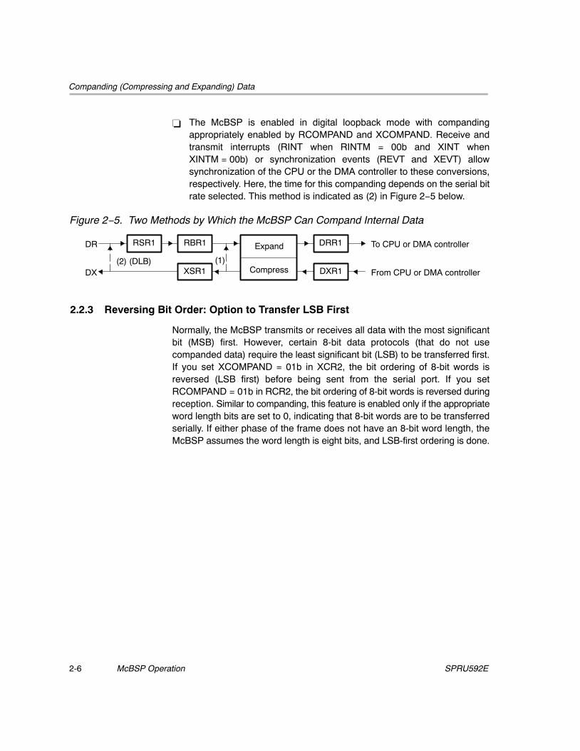
Companding (Compressing and Expanding) Data
McBSP Operation2-6 SPRU592E
� The McBSP is enabled in digital loopback mode with compandingappropriately enabled by RCOMPAND and XCOMPAND. Receive andtransmit interrupts (RINT when RINTM = 00b and XINT whenXINTM = 00b) or synchronization events (REVT and XEVT) allowsynchronization of the CPU or the DMA controller to these conversions,respectively. Here, the time for this companding depends on the serial bitrate selected. This method is indicated as (2) in Figure 2−5 below.
Figure 2−5. Two Methods by Which the McBSP Can Compand Internal Data
(1)(2) (DLB)From CPU or DMA controllerDXR1
To CPU or DMA controllerDRR1
DX XSR1 Compress
ExpandDR RBR1RSR1
2.2.3 Reversing Bit Order: Option to Transfer LSB First
Normally, the McBSP transmits or receives all data with the most significantbit (MSB) first. However, certain 8-bit data protocols (that do not usecompanded data) require the least significant bit (LSB) to be transferred first.If you set XCOMPAND = 01b in XCR2, the bit ordering of 8-bit words isreversed (LSB first) before being sent from the serial port. If you setRCOMPAND = 01b in RCR2, the bit ordering of 8-bit words is reversed duringreception. Similar to companding, this feature is enabled only if the appropriateword length bits are set to 0, indicating that 8-bit words are to be transferredserially. If either phase of the frame does not have an 8-bit word length, theMcBSP assumes the word length is eight bits, and LSB-first ordering is done.
Clocking and Framing Data
2-7McBSP OperationSPRU592E
2.3 Clocking and Framing DataThis section explains basic concepts and terminology important forunderstanding how McBSP data transfers are timed and delimited.
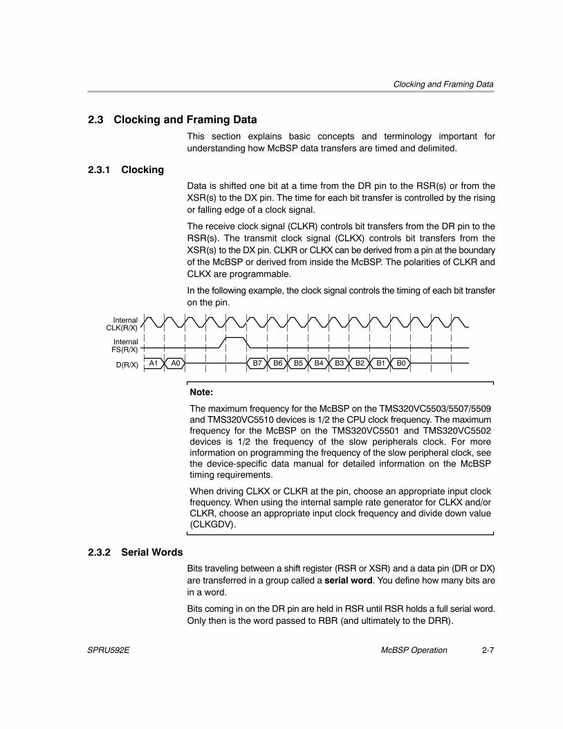
2.3.1 Clocking
Data is shifted one bit at a time from the DR pin to the RSR(s) or from theXSR(s) to the DX pin. The time for each bit transfer is controlled by the risingor falling edge of a clock signal.
The receive clock signal (CLKR) controls bit transfers from the DR pin to theRSR(s). The transmit clock signal (CLKX) controls bit transfers from theXSR(s) to the DX pin. CLKR or CLKX can be derived from a pin at the boundaryof the McBSP or derived from inside the McBSP. The polarities of CLKR andCLKX are programmable.
In the following example, the clock signal controls the timing of each bit transferon the pin.
D(R/X)
FS(R/X)
CLK(R/X)
B0B1B2B3B4B5B6B7A0A1 ÁÁÁÁ
ÁÁ
ÁÁÁÁ
Internal
Internal
Note:
The maximum frequency for the McBSP on the TMS320VC5503/5507/5509and TMS320VC5510 devices is 1/2 the CPU clock frequency. The maximumfrequency for the McBSP on the TMS320VC5501 and TMS320VC5502devices is 1/2 the frequency of the slow peripherals clock. For moreinformation on programming the frequency of the slow peripheral clock, seethe device-specific data manual for detailed information on the McBSPtiming requirements.
When driving CLKX or CLKR at the pin, choose an appropriate input clockfrequency. When using the internal sample rate generator for CLKX and/orCLKR, choose an appropriate input clock frequency and divide down value(CLKGDV).
2.3.2 Serial Words
Bits traveling between a shift register (RSR or XSR) and a data pin (DR or DX)are transferred in a group called a serial word. You define how many bits arein a word.
Bits coming in on the DR pin are held in RSR until RSR holds a full serial word.Only then is the word passed to RBR (and ultimately to the DRR).

Clocking and Framing Data
McBSP Operation2-8 SPRU592E
During transmission, XSR does not accept new data from DXR until a full serialword has been passed from XSR to the DX pin.
In the following example, an 8-bit word size was defined (see bits 7 through0 of word B being transferred).
D(R/X)
FS(R/X)
CLK(R/X)
B0B1B2B3B4B5B6B7A0A1ÁÁ
ÁÁ
ÁÁ
Internal
Internal
2.3.3 Frames and Frame Synchronization
One or more words are transferred in a group called a frame. You define howmany words are in a frame.
All of the words in a frame are sent in a continuous stream. However, there canbe pauses between frame transfers. The McBSP uses frame-synchronization(frame-sync) signals to determine when each frame is received/transmitted.When a pulse occurs on a frame-sync signal, the McBSP beginsreceiving/transmitting a frame of data. When the next pulse occurs, theMcBSP receives/transmits the next frame, and so on.
Pulses on the receive frame-sync signal (FSR) initiate frame transfers on DR.Pulses on the transmit frame-sync signal (FSX) initiate frame transfers on DX.FSR or FSX can be derived from a pin at the boundary of the McBSP or derivedfrom inside the McBSP.
In the following example, a 1-word frame is transferred when a frame-syncpulse occurs.
D(R/X)
FS(R/X)
CLK(R/X)
B0B1B2B3B4B5B6B7A0A1ÁÁ
ÁÁ
ÁÁ
Internal
Internal
In McBSP operation, the inactive-to-active transition of theframe-synchronization signal indicates the start of the next frame. For thisreason, the frame-sync signal may be high for an arbitrary number of clockcycles. Only after the signal is recognized to have gone inactive, and thenactive again, does the next frame synchronization occur.

Clocking and Framing Data
2-9McBSP OperationSPRU592E
2.3.4 Detecting Frame-Sync Pulses, Even in the Reset State
The McBSP can send receive and transmit interrupts to the CPU to indicatespecific events in the McBSP. To facilitate detection of frame synchronization,these interrupts can be sent in response to frame-sync pulses. Set theappropriate interrupt mode bits to 10b (for reception, RINTM = 10b; fortransmission, XINTM = 10b).
Unlike other serial port interrupt modes, this mode can operate while theassociated portion of the serial port is in reset (such as activating RINT whenthe receiver is in reset). In this case, FSRM/FSXM and FSRP/FSXP still selectthe appropriate source and polarity of frame synchronization. Thus, evenwhen the serial port is in the reset state, these signals are synchronized to theMcBSP internal input clock and then sent to the CPU in the form of RINT andXINT at the point at which they feed the receiver and transmitter of the serialport. Consequently, a new frame-synchronization pulse can be detected, andafter this occurs the CPU can take the serial port out of reset safely.
2.3.5 Ignoring Unexpected Frame-Sync Pulses
The McBSP can be configured to ignore transmit and/or receiveframe-synchronization pulses. To have the receiver or transmitter recognizeframe-sync pulses, clear the appropriate frame-sync ignore bit (RFIG = 0 forthe receiver, XFIG = 0 for the transmitter). To have the receiver or transmitterignore frame-sync pulses until the desired frame length or number of wordsis reached, set the appropriate frame-sync ignore bit (RFIG = 1 for thereceiver, XFIG = 1 for the transmitter).
2.3.6 Frame Frequency
The frame frequency is determined by the period betweenframe-synchronization pulses and is defined as shown by Equation 2−1.
Equation 2−1. Frame Frequency of a McBSP
Frame Frequency �Clock Frequency
Number of Clock Cycles Between Frame−Sync Pulses
The frame frequency can be increased by decreasing the time betweenframe-synchronization pulses (limited only by the number of bits per frame).As the frame transmit frequency increases, the inactivity period between thedata packets for adjacent transfers decreases to zero.
2.3.7 Maximum Frame Frequency
The minimum number of clock cycles between frame synchronization pulsesis equal to the number of bits transferred per frame. The maximum framefrequency is defined as shown by Equation 2−2.

Clocking and Framing Data
McBSP Operation2-10 SPRU592E
Equation 2−2. Maximum Frame Frequency of a McBSP
Maximum Frame Frequency �Clock Frequency
Number of Bits Per Frame
Figure 2−6 shows the McBSP operating at maximum packet frequency. Atmaximum packet frequency, the data bits in consecutive packets aretransmitted contiguously with no inactivity between bits.
Figure 2−6. McBSP Operating at Maximum Packet Frequency
D(R/X)
FS(R/X)
CLK(R/X)
C6C7B0B1B2B3B4B5B6B7A0A1A2
If there is a 1-bit data delay as shown in this figure, the frame-synchronizationpulse overlaps the last bit transmitted in the previous frame. Effectively, thispermits a continuous stream of data, making frame-synchronization pulsesredundant. Theoretically, only an initial frame-synchronization pulse isrequired to initiate a multipacket transfer.
The McBSP supports operation of the serial port in this fashion by ignoring thesuccessive frame-sync pulses. Data is clocked in to the receiver, or clockedout of the transmitter, during every clock cycle.
Note:
For XDATDLY = 0 (0-bit data delay), the first bit of data is transmittedasynchronously to the internal transmit clock signal (CLKX).
Note:
On the TMS320VC5501 and TMS320VC5502 devices, if a 0-bit delay andan external clock are used, the transfer shown in Figure 2−6 can only beachieved if the frame-sync ignore bit is set to 1. If the frame-sync ignore bitis 0, an additional clock cycle is required between frames.

Frame Phases
2-11McBSP OperationSPRU592E
2.4 Frame Phases
The McBSP allows you to configure each frame to contain one or two phases.The number of words per frame, and the number of bits per word, can bespecified differently for each of the two phases of a frame, allowing greaterflexibility in structuring data transfers. For example, a user might define aframe as consisting of one phase containing two words of 16 bits each,followed by a second phase consisting of 10 words of 8 bits each. Thisconfiguration permits the user to compose frames for custom applications, orin general, to maximize the efficiency of data transfers.
2.4.1 Number of Phases, Words, and Bits Per Frame
Table 2−1 shows which bit fields in the receive control registers (RCR1 andRCR2) and in the transmit control registers (XCR1 and XCR2) determine thenumber of phases per frame, the number of words per frame, and number ofbits per word for each phase, for the receiver and transmitter. The maximumnumber of words per frame is 128 for a single-phase frame and 256 for adual-phase frame. The number of bits per word can be 8, 12, 16, 20, 24, or 32bits. The maximum number of bits (serial port clock cycles) per frame is 4096.
Table 2−1. McBSP Register Bits That Determine the Number of Phases, Words, andBits Per Frame
Operation Number of PhasesWords Per FrameSet With ...
Bits Per WordSet With ...
Reception 1 (RPHASE = 0) RFRLEN1 RWDLEN1
Reception 2 (RPHASE = 1) RFRLEN1 andRFRLEN2
RWDLEN1 for phase 1RWDLEN2 for phase 2
Transmission 1 (XPHASE = 0) XFRLEN1 XWDLEN1
Transmission 2 (XPHASE = 1) XFRLEN1 andXFRLEN2
XWDLEN1 for phase 1XWDLEN2 for phase 2
2.4.2 Single-Phase Frame Example
Figure 2−7 shows an example of a single-phase data frame comprising one8-bit word. Since the transfer is configured for one data bit delay, the data onthe DX and DR pins are available one clock cycle after FS(R/X) goes active.The figure makes the following assumptions:
� (R/X)PHASE = 0: Single-phase frame
� (R/X)FRLEN1 = 0b: 1 word per frame

Frame Phases
McBSP Operation2-12 SPRU592E
� (R/X)WDLEN1 = 000b: 8-bit word length
� (R/X)FRLEN2 and (R/X)WDLEN2 are ignored
� CLK(X/R)P = 0: Receive data clocked on falling edge; transmit dataclocked on rising edge
� FS(R/X)P = 0: Active-high frame-sync signals
� (R/X)DATDLY = 01b: 1-bit data delay
Figure 2−7. Single-Phase Frame for a McBSP Data Transfer
A1D(R/X)
FS(R/X)
CLK(R/X)
C5C6C7B0B1B2B3B4B5B6B7A0 ÁÁÁÁÁ
2.4.3 Dual-Phase Frame Example
Figure 2−8 shows an example of a frame where the first phase consists of 2words of 12 bits each, followed by a second phase of three words of 8 bitseach. Note that the entire bit stream in the frame is contiguous. There are nogaps either between words or between phases.
Figure 2−8. Dual-Phase Frame for a McBSP Data Transfer
D(R/X)
FS(R/X)
CLK(R/X)
Phase 2word 3Phase 2
word 2
Phase 2word 1
ÁÁÁÁ
ÁÁÁÁ
ÁÁÁÁÁÁ
ÁÁ
ÁÁÁÁ
ÁÁÁÁÁÁÁÁÁÁÁÁ
ÁÁ
ÁÁÁÁÁÁ
ÁÁÁÁÁÁÁÁ
ÁÁÁÁ
ÁÁÁÁ
ÁÁÁÁÁÁ
ÁÁÁÁ
ÁÁ
ÁÁÁÁÁÁÁÁÁÁ
ÁÁÁÁÁÁÁÁ
ÁÁÁÁÁÁÁÁ
ÁÁÁÁÁÁÁÁÁÁ
ÁÁÁÁÁÁÁÁ
ÁÁÁÁ
ÁÁÁÁÁÁ
ÁÁÁÁÁÁÁÁÁÁ
ÁÁÁÁÁÁÁÁ
ÁÁÁÁ
ÁÁÁÁÁÁÁÁ
ÁÁÁÁÁÁ
ÁÁ
ÁÁÁÁ
Phase 1 word 1Phase 1 word 2
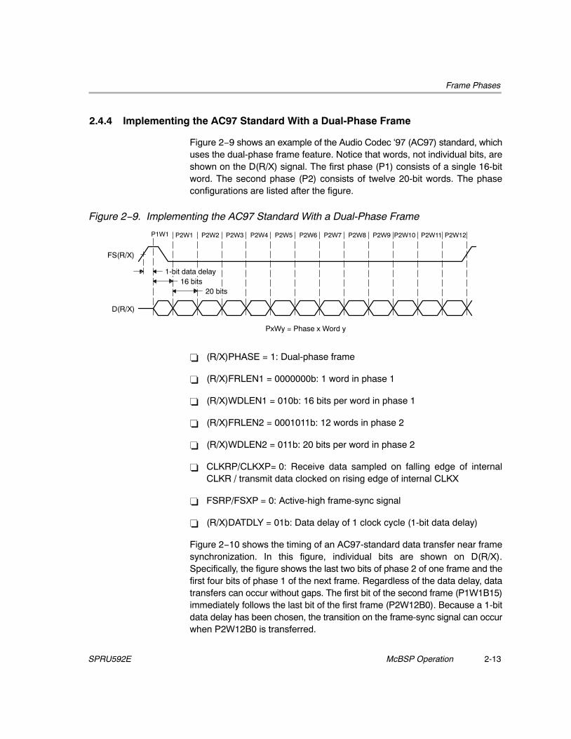
Frame Phases
2-13McBSP OperationSPRU592E
2.4.4 Implementing the AC97 Standard With a Dual-Phase Frame
Figure 2−9 shows an example of the Audio Codec ‘97 (AC97) standard, whichuses the dual-phase frame feature. Notice that words, not individual bits, areshown on the D(R/X) signal. The first phase (P1) consists of a single 16-bitword. The second phase (P2) consists of twelve 20-bit words. The phaseconfigurations are listed after the figure.
Figure 2−9. Implementing the AC97 Standard With a Dual-Phase Frame
PxWy = Phase x Word y
D(R/X)
FS(R/X)
P2W12P2W11P2W10P2W9P2W8P2W7P2W6P2W5P2W4P2W3P2W2P2W1P1W1
ÁÁÁÁ
20 bits16 bits
1-bit data delay
� (R/X)PHASE = 1: Dual-phase frame
� (R/X)FRLEN1 = 0000000b: 1 word in phase 1
� (R/X)WDLEN1 = 010b: 16 bits per word in phase 1
� (R/X)FRLEN2 = 0001011b: 12 words in phase 2
� (R/X)WDLEN2 = 011b: 20 bits per word in phase 2
� CLKRP/CLKXP= 0: Receive data sampled on falling edge of internalCLKR / transmit data clocked on rising edge of internal CLKX
� FSRP/FSXP = 0: Active-high frame-sync signal
� (R/X)DATDLY = 01b: Data delay of 1 clock cycle (1-bit data delay)
Figure 2−10 shows the timing of an AC97-standard data transfer near framesynchronization. In this figure, individual bits are shown on D(R/X).Specifically, the figure shows the last two bits of phase 2 of one frame and thefirst four bits of phase 1 of the next frame. Regardless of the data delay, datatransfers can occur without gaps. The first bit of the second frame (P1W1B15)immediately follows the last bit of the first frame (P2W12B0). Because a 1-bitdata delay has been chosen, the transition on the frame-sync signal can occurwhen P2W12B0 is transferred.

Frame Phases
McBSP Operation2-14 SPRU592E
Figure 2−10. Timing of an AC97-Standard Data Transfer Near Frame Synchronization
PxWyBz = Phase x Word y Bit z
ÁÁÁÁ P2W12B0P2W12B1DR P1W1B15 P1W1B12P1W1B13P1W1B14
FSR
CLKR
1-bit data delay
Note:
On the TMS320VC5501 and TMS320VC5502 devices, if a 0-bit delay andan external clock are used, the transfer shown in Figure 2−9 can only beachieved if the frame-sync ignore bit is set to 1. If the frame-sync ignore bitis 0, an additional clock cycle is required between frames.
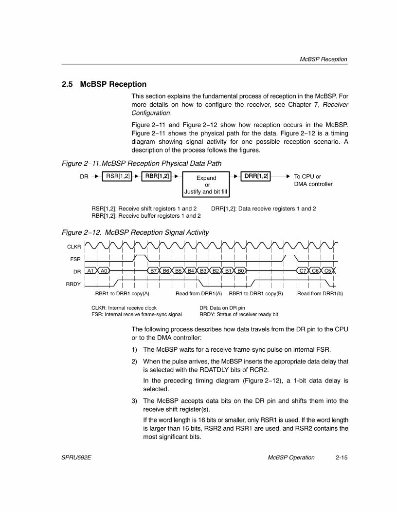
McBSP Reception
2-15McBSP OperationSPRU592E
2.5 McBSP Reception
This section explains the fundamental process of reception in the McBSP. Formore details on how to configure the receiver, see Chapter 7, ReceiverConfiguration.
Figure 2−11 and Figure 2−12 show how reception occurs in the McBSP.Figure 2−11 shows the physical path for the data. Figure 2−12 is a timingdiagram showing signal activity for one possible reception scenario. Adescription of the process follows the figures.
Figure 2−11.McBSP Reception Physical Data Path
ÁÁÁÁÁÁÁÁ
ÁÁÁÁÁÁÁÁ
DR RSR[1,2] Expand ÁÁÁÁÁÁÁÁ
RBR[1,2] DRR[1,2]DRR[1,2]RBR[1,2] To CPU orDMA controller
Justify and bit fillor
RSR[1,2]: Receive shift registers 1 and 2RBR[1,2]: Receive buffer registers 1 and 2
DRR[1,2]: Data receive registers 1 and 2
Figure 2−12. McBSP Reception Signal Activity
RRDY
DR
FSR
CLKR
Read from DRR1(b)RBR1 to DRR1 copy(B)Read from DRR1(A)RBR1 to DRR1 copy(A)
C5C6C7B0B1B2B3B4B5B6B7A0A1ÁÁÁÁ
ÁÁ
ÁÁ
ÁÁÁÁ
CLKR: Internal receive clockFSR: Internal receive frame-sync signal
DR: Data on DR pinRRDY: Status of receiver ready bit
The following process describes how data travels from the DR pin to the CPUor to the DMA controller:
1) The McBSP waits for a receive frame-sync pulse on internal FSR.
2) When the pulse arrives, the McBSP inserts the appropriate data delay thatis selected with the RDATDLY bits of RCR2.
In the preceding timing diagram (Figure 2−12), a 1-bit data delay isselected.
3) The McBSP accepts data bits on the DR pin and shifts them into thereceive shift register(s).
If the word length is 16 bits or smaller, only RSR1 is used. If the word lengthis larger than 16 bits, RSR2 and RSR1 are used, and RSR2 contains themost significant bits.

McBSP Reception
McBSP Operation2-16 SPRU592E
4) When a full word is received, the McBSP copies the contents of the receiveshift register(s) to the receive buffer register(s), provided that RBR1 is notfull with previous data.
If the word length is 16 bits or smaller, only RBR1 is used. If the word lengthis larger than 16 bits, RBR2 and RBR1 are used, and RBR2 contains themost significant bits.
5) The McBSP copies the contents of the receive buffer register(s) into thedata receive register(s), provided that DRR1 is not full with previous data.When DRR1 receives new data, the receiver ready bit (RRDY) is set inSPCR1. This indicates that receive data is ready to be read by the CPUor the DMA controller.
If the word length is 16 bits or smaller, only DRR1 is used. If the word lengthis larger than 16 bits, DRR2 and DRR1 are used, and DRR2 contains themost significant bits.
If companding is used during the copy (RCOMPAND = 10b or 11b inRCR2), the 8-bit compressed data in RBR1 is expanded to a left-justified16-bit value in DRR1. If companding is disabled, the data copied fromRBR[1,2] to DRR[1,2] is justified and bit filled according to the RJUST bits.
6) The CPU or the DMA controller reads the data from the data receiveregister(s). When DRR1 is read, RRDY is cleared and the nextRBR-to-DRR copy is initiated.
Note:
If both DRRs are needed (word length larger than 16 bits), the CPU or theDMA controller must read from DRR2 first and then from DRR1. As soon asDRR1 is read, the next RBR-to-DRR copy is initiated. If DRR2 is not readfirst, the data in DRR2 is lost.
When activity is not properly timed, errors can occur. See the following topicsin Chapter 4 for more details:
� Overrun in the Receiver
� Unexpected Receive Frame-Sync Pulse

McBSP Transmission
2-17McBSP OperationSPRU592E
2.6 McBSP Transmission
This section explains the fundamental process of transmission in the McBSP.For details about how to program the McBSP transmitter, see Chapter 8,Transmitter Configuration.
Figure 2−13 and Figure 2−14 show how transmission occurs in the McBSP.Figure 2−13 shows the physical path for the data. Figure 2−14 is a timingdiagram showing signal activity for one possible transmission scenario. Adescription of the process follows the figures.
Figure 2−13. McBSP Transmission Physical Data Path
ÁÁÁÁÁÁÁÁ
DX XSR[1,2] ÁÁÁÁÁÁ
DXR[1,2] From CPU orDMA controller
Compress
Do not modifyor
XSR[1,2]: Transmit shift registers 1 and 2 DXR[1,2]: Data transmit registers 1 and 2
Figure 2−14. McBSP Transmission Signal Activity
Write to DXR1DXR1 to XSR1 copy(C)Write to DXR1(C)DXR1 to XSR1 copy(B)
XRDY
DX
FSX
CLKX
C5C6C7B0B1B2B3B4B5B6B7A0A1 ÁÁ
ÁÁÁÁ
ÁÁ
ÁÁ
CLKX: Internal transmit clockFSX: Internal transmit frame-sync signal
DX: Data on DX pinXRDY: Status of transmitter ready bit (high is 1)
1) The CPU or the DMA controller writes data to the data transmit register(s).When DXR1 is loaded, the transmitter ready bit (XRDY) is cleared inSPCR2 to indicate that the transmitter is not ready for new data.
If the word length is 16 bits or smaller, only DXR1 is used. If the word lengthis larger than 16 bits, DXR2 and DXR1 are used, and DXR2 contains themost significant bits.
Note:
If both DXRs are needed (word length larger than 16 bits), the CPU or theDMA controller must load DXR2 first and then load DXR1. As soon as DXR1is loaded, the contents of both DXRs are copied to the transmit shift registers(XSRs), as described in the next step. If DXR2 is not loaded first, the previouscontent of DXR2 is passed to the XSR2.

McBSP Transmission
McBSP Operation2-18 SPRU592E
2) When new data arrives in DXR1, the McBSP copies the content of the datatransmit register(s) to the transmit shift register(s). In addition, the transmitready bit (XRDY) is set. This indicates that the transmitter is ready toaccept new data from the CPU or the DMA controller.
If the word length is 16 bits or smaller, only XSR1 is used. If the word lengthis larger than 16 bits, XSR2 and XSR1 are used, and XSR2 contains themost significant bits.
If companding is used during the transfer (XCOMPAND = 10b or 11b inXCR2), the McBSP compresses the 16-bit data in DXR1 to 8-bit data in theµ-law or A-law format in XSR1. If companding is disabled, the McBSPpasses data from the DXR(s) to the XSR(s) without modification.
3) The McBSP waits for a transmit frame-sync pulse on internal FSX.
4) When the pulse arrives, the McBSP inserts the appropriate data delay thatis selected with the XDATDLY bits of XCR2.
In the preceding timing diagram (Figure 2−14), a 1-bit data delay isselected.
5) The McBSP shifts data bits from the transmit shift register(s) to the DX pin.
When activity is not properly timed, errors can occur. See the following topicsin Chapter 4 for more details:
� Overwrite in the Transmitter
� Underflow in the Transmitter
� Unexpected Transmit Frame-Sync Pulse

Interrupts and DMA Events Generated by a McBSP
2-19McBSP OperationSPRU592E
2.7 Interrupts and DMA Events Generated by a McBSP
The McBSP sends notification of important events to the CPU and the DMAcontroller via the internal signals shown in Table 2−2.
Table 2−2. Interrupts and DMA Events Generated by a McBSP
Internal Signal Description
RINT Receive interrupt
The McBSP can send a receive interrupt request to CPU basedupon a selected condition in the receiver of the McBSP (acondition selected by the RINTM bits of SPCR1).
XINT Transmit interrupt
The McBSP can send a transmit interrupt request to CPU basedupon a selected condition in the transmitter of the McBSP (acondition selected by the XINTM bits of SPCR2).
REVT Receive synchronization event
An REVT signal is sent to the DMA controller when data hasbeen received in the data receive registers (DRRs).
XEVT Transmit synchronization event
An XEVT signal is sent to the DMA controller when the datatransmit registers (DXRs) are ready to accept the next serialword for transmission.

McBSP Operation2-20 SPRU592E
This page is intentionally left blank.
3-1
Sample Rate Generator of the McBSP
This chapter gives information on the use of the sample rate generator to driveclocking, and provides the appropriate clocking examples for support.
Topic Page
3.1 Sample Rate Generator 3-2. . . . . . . . . . . . . . . . . . . . . . . . . . . . . . . . . . . . . . . .
3.2 Clock Generation in the Sample Rate Generator 3-4. . . . . . . . . . . . . . . . .
3.3 Frame Sync Generation in the Sample Rate Generator 3-9. . . . . . . . . . .
3.4 Synchronizing Sample Rate Generator Outputs to an External Clock 3-10. . . . . . . . . . . . . . . . . . . . . . . . . . . . . . . . . . . . . . . . . . . . . . .
3.5 Reset and Initialization Procedure for the Sample Rate Generator 3-12. . . . . . . . . . . . . . . . . . . . . . . . . . . . . . . . . . . . . . . . . . . . . . . . . . .
3.6 Sample Rate Generator Clocking Examples 3-14. . . . . . . . . . . . . . . . . . . .
Chapter 3

Sample Rate Generator
Sample Rate Generator of the McBSP3-2 SPRU592E
3.1 Sample Rate Generator
Each McBSP contains a sample rate generator that can be used to generatean internal data clock (CLKG) and an internal frame-synchronization signal(FSG). CLKG can be used for bit shifting on the data receive (DR) pin and/orthe data transmit (DX) pin. FSG can be used to initiate frame transfers on DRand/or DX. Figure 3−1 is a conceptual block diagram of the sample rategenerator.
Figure 3−1. Conceptual Block Diagram of the Sample Rate Generator
FSR
GSYNC synchronization¶and clockdetection
Frame pulse
FWID
CLKG
FSGPulseFrame
FPERCLKGDV
CLKSRG ÷ ÷0
1CLKXP†
CLKX pin
CLKRP†
CLKR pin
0
1McBSP internal
CLKSP§
CLKS pin§
CLKSM
0
1
SCLKMEinput clock‡
† On TMS320VC5501 and TMS320VC5502 devices, the polarity of the sample rate generator input clock (CLKSRG) is alwayspositive (rising edge), regardless of CLKRP or CLKXP.
‡ McBSP internal input clock: On TMS320VC5503/5507/5509 and TMS320VC5510 devices, this clock is the CPU clock. OnTMS320VC5501 and TMS320VC5502 devices, this clock is the slow peripherals clock.
§ Not all C55x devices have a CLKS pin; check the device-specific data manual.¶ The clock synchronization provided through the GSYNC bit is not supported on TMS320VC5501 and TMS320VC5502 devices.

Sample Rate Generator
3-3Sample Rate Generator of the McBSPSPRU592E
The input clock for the sample rate generator (labeled CLKSRG in Figure 3−1)can be supplied by the McBSP internal input clock or by one of these externalpins: CLKX, CLKR, or (if present) CLKS. Not all C55x devices have a CLKSpin; check the device-specific data manual. The input clock source is selectedwith the SCLKME bit of PCR and the CLKSM bit of SRGR2. If a pin is used,the polarity of the incoming signal can be inverted with the appropriate polaritybit (CLKXP of PCR, CLKRP of PCR, or CLKSP of SRGR2).
Note:
On TMS320VC5501 and TMS320VC5502 devices, the polarity of thesample rate generator input clock is always positive (rising edge), regardlessof CLKRP or CLKXP.
The sample rate generator has a 3-stage clock divider that gives CLKG andFSG programmability. The three stages provide:
� Clock divide down. The sample rate generator input clock is dividedaccording to the CLKGDV bits of SRGR1 to produce CLKG.
� Frame period divide down. CLKG is divided according to the FPER bits ofSRGR2 to control the period from the start of a frame-sync pulse to thestart of the next pulse.
� Frame-sync pulse width countdown. CLKG cycles are counted accordingto the FWID bits of SRGR1 to control the width of each frame-sync pulse.
Note:
The maximum frequency for the McBSP on the TMS320VC5503/5507/5509and TMS320VC5510 devices is 1/2 the CPU clock frequency. The maximumfrequency for the McBSP on the TMS320VC5501 and TMS320VC5502devices is 1/2 the frequency of the slow peripherals clock. For moreinformation on programming the frequency of the slow peripheral clock, seethe TMS320VC5501 Fixed-Point Digital Signal Processor Data Manual(literature number SPRS206) or the TMS320VC5502 Fixed-Point DigitalSignal Processor Data Manual (literature number SPRS166). Other timinglimitations may also apply. See the device-specific data manual for detailedinformation on the McBSP timing requirements.
When driving CLKX or CLKR at the pin, choose an appropriate input clockfrequency. When using the internal sample rate generator for CLKX and/orCLKR, choose an appropriate input clock frequency and divide down value(CLKGDV).

Clock Generation in the Sample Rate Generator
Sample Rate Generator of the McBSP3-4 SPRU592E
In addition to the three-stage clock divider, the sample rate generator has aframe-sync pulse detection and clock synchronization module that allowssynchronization of the clock divide down with an incoming frame-sync pulseon the FSR pin. This feature is enabled or disabled with the GSYNC bit ofSRGR2.
Note:
The clock synchronization provided through the GSYNC bit is not supportedon TMS320VC5501 and TMS320VC5502 devices.
3.2 Clock Generation in the Sample Rate Generator
The sample rate generator can produce a clock signal (CLKG) for use by thereceiver, the transmitter, or both. Use of the sample rate generator to driveclocking is controlled by the clock mode bits (CLKRM and CLKXM) in the pincontrol register (PCR). When a clock mode bit is set to 1 (CLKRM = 1 forreception, CLKXM = 1 for transmission), the corresponding data clock (CLKRfor reception, CLKX for transmission) is driven by the internal sample rategenerator output clock (CLKG).
Note that the effects of CLKRM = 1 and CLKXM = 1 on the McBSP arepartially affected by the use of the digital loopback mode and the clock stop(SPI) mode, respectively. The digital loopback mode is selected with the DLBbit of SPCR1. The clock stop mode is selected with the CLKSTP bits ofSPCR1.
When using the sample rate generator as a clock source, make sure thesample rate generator is enabled (GRST = 1).
Table 3−1. Effects of DLB and CLKSTP on Clock Modes
Mode Bit Settings Effect
CLKRM = 1 DLB = 0(Digital loopback mode disabled)
CLKR is an output pin driven by the sample rategenerator output clock (CLKG).
DLB = 1(Digital loopback mode enabled)
CLKR is an output pin driven by internal CLKX. Thesource for CLKX depends on the CLKXM bit.
CLKXM = 1 CLKSTP = 00b or 01b(Clock stop (SPI) mode disabled)
CLKX is an output pin driven by the sample rategenerator output clock (CLKG).
CLKSTP = 10b or 11b(Clock stop (SPI) mode enabled)
The McBSP is a master in an SPI system. InternalCLKX drives internal CLKR and the shift clocks of anySPI-compliant slave devices in the system. CLKX isdriven by the internal sample rate generator.

Clock Generation in the Sample Rate Generator
3-5Sample Rate Generator of the McBSPSPRU592E
3.2.1 Choosing an Input Clock
The sample rate generator must be driven by an input clock signal from oneof the four sources selectable with the SCLKME bit of PCR and the CLKSMbit of SRGR2 (see Table 3−2). When CLKSM = 1, the minimum divide downvalue in CLKGDV bits should be 1.
Note:
The maximum frequency for the McBSP on the TMS320VC5503/5507/5509and TMS320VC5510 devices is 1/2 the CPU clock frequency. The maximumfrequency for the McBSP on the TMS320VC5501 and TMS320VC5502devices is 1/2 the frequency of the slow peripherals clock. For moreinformation on programming the frequency of the slow peripheral clock, seethe TMS320VC5501 Fixed-Point Digital Signal Processor Data Manual(literature number SPRS206) or the TMS320VC5502 Fixed-Point DigitalSignal Processor Data Manual (literature number SPRS166). Other timinglimitations may also apply. See the device-specific data manual for detailedinformation on the McBSP timing requirements.
When driving CLKX or CLKR at the pin, choose an appropriate input clockfrequency. When using the internal sample rate generator for CLKX and/orCLKR, choose an appropriate input clock frequency and divide down value(CLKGDV).
Table 3−2. Choosing an Input Clock for the Sample Rate Generator With the SCLKME and CLKSM Bits
SCLKME CLKSMInput Clock ForSample Rate Generator
0 0 Signal on CLKS pin
0 1 McBSP internal input clock
1 0 Signal on CLKR pin
1 1 Signal on CLKX pin

Clock Generation in the Sample Rate Generator
Sample Rate Generator of the McBSP3-6 SPRU592E
3.2.2 Choosing a Polarity for the Input Clock
As shown in Figure 3−2, when the input clock is received from a pin, you canchoose the polarity of the input clock. The rising edge of CLKSRG generatesCLKG and FSG, but you can determine which edge of the input clock causesa rising edge on CLKSRG. The polarity options and their effects are describedin Table 3−3.
Figure 3−2. Possible Inputs to the Sample Rate Generator and the Polarity Bits
CLKSRG
0
1CLKXP†
CLKX pin
CLKRP†
CLKR pin
0
1
CLKSP§
CLKS pin§
CLKSM
0
1
SCLKME
To clock dividersfor CLKG and FSG
McBSP internalinput clock‡
† On TMS320VC5501 and TMS320VC5502 devices, the polarity of the sample rate generator input clock (CLKSRG) is alwayspositive (rising edge), regardless of CLKRP or CLKXP.
‡ McBSP internal input clock: On TMS320VC5503/5507/5509 and TMS320VC5510 devices, this clock is the CPU clock. OnTMS320VC5501 and TMS320VC5502 devices, this clock is the slow peripherals clock.
§ Not all C55x devices have a CLKS pin; check the device-specific data manual.

Clock Generation in the Sample Rate Generator
3-7Sample Rate Generator of the McBSPSPRU592E
Table 3−3. Polarity Options for the Input to the Sample Rate Generator
Input Clock Polarity Option Effect
on CLKS pin† CLKSP = 0 in SRGR2 Rising edge on CLKS pin generates rising edge on CLKG.Rising edge on CLKS pin generates transitions on FSG.
CLKSP = 1 in SRGR2 Falling edge on CLKS pin generates rising edge on CLKG.Falling edge on CLKS pin generates transitions on FSG.
McBSP internalinput clock
Always positive polarity Rising edge of McBSP internal input clock generates risingedge on CLKG.
on CLKR pin CLKRP‡= 0 in PCR Rising edge on CLKR pin generates rising edge on CLKG.Rising edge on CLKR pin generates transitions on FSG.
CLKRP‡= 1 in PCR Falling edge on CLKR pin generates rising edge on CLKG.Falling edge on CLKR pin generates transitions on FSG.
on CLKX pin CLKXP‡= 0 in PCR Rising edge on CLKX pin generates rising edge on CLKG.Rising edge on CLKX pin generates transitions on FSG.
CLKXP‡= 1 in PCR Falling edge on CLKX pin generates rising edge on CLKG.Falling edge on CLKX pin generates transitions on FSG.
† Not all C55x devices have a CLKS pin; check the device-specific data manual.‡ On TMS320VC5501 and TMS320VC5502 devices, the polarity of the sample rate generator input clock is always positive (rising
edge), regardless of CLKRP or CLKXP.
3.2.3 Choosing a Frequency for the Output Clock (CLKG)
The input clock (McBSP internal input clock or external clock) can be divideddown by a programmable value to drive CLKG. Regardless of the source tothe sample rate generator, the rising edge of CLKSRG generates CLKG andFSG.
The first divider stage of the sample rate generator creates the output clockfrom the input clock. This divider stage uses a counter that is preloaded withthe divide down value in the CLKGDV bits of SRGR1. The output of this stageis the data clock (CLKG). CLKG has the frequency represented by thefollowing equation.
CLKG frequency �Input clock frequency
(CLKGDV � 1)
Thus, the input clock frequency is divided by a value between 1 and 256. WhenCLKGDV is odd or equal to 0, the CLKG duty cycle is 50%. When CLKGDVis an even value, 2p, representing an odd divide down, the high-state durationis p+1 cycles and the low-state duration is p cycles.

Clock Generation in the Sample Rate Generator
Sample Rate Generator of the McBSP3-8 SPRU592E
Note:
The maximum frequency for the McBSP on the TMS320VC5503/5507/5509and TMS320VC5510 devices is 1/2 the CPU clock frequency. The maximumfrequency for the McBSP on the TMS320VC5501 and TMS320VC5502devices is 1/2 the frequency of the slow peripherals clock. For moreinformation on programming the frequency of the slow peripheral clock, seethe TMS320VC5501 Fixed-Point Digital Signal Processor Data Manual(literature number SPRS206) or the TMS320VC5502 Fixed-Point DigitalSignal Processor Data Manual (literature number SPRS166). Other timinglimitations may also apply. See the device-specific data manual for detailedinformation on the McBSP timing requirements.
When driving CLKX or CLKR at the pin, choose an appropriate input clockfrequency. When using the internal sample rate generator for CLKX and/orCLKR, choose an appropriate input clock frequency and divide down value(CLKGDV).
3.2.4 Keeping CLKG Synchronized to an External Input Clock
When an external signal is selected to drive the sample rate generator, theGSYNC bit in SRGR2 and the FSR pin can be used to configure the timing ofthe output clock (CLKG) relative to the input clock.
GSYNC = 1 ensures that the McBSP and an external device are dividing downthe input clock with the same phase relationship. If GSYNC = 1, aninactive-to-active transition on the FSR pin triggers a resynchronization ofCLKG and generation of FSG.
Note:
The clock synchronization provided through the GSYNC bit is not supportedon TMS320VC5501 and TMS320VC5502 devices.

Frame Sync Generation in the Sample Rate Generator
3-9Sample Rate Generator of the McBSPSPRU592E
3.3 Frame Sync Generation in the Sample Rate Generator
The sample rate generator can produce a frame-sync signal (FSG) for use bythe receiver, the transmitter, or both.
If you want the receiver to use FSG for frame synchronization, set FSRM = 1.(When FSRM = 0, receive frame synchronization is supplied via the FSR pin.)
If you want the transmitter to use FSG for frame synchronization, you mustset:
� FSXM = 1 in PCR: This indicates that transmit frame synchronization issupplied by the McBSP itself rather than from the FSX pin.
� FSGM = 1 in SRGR2: This indicates that when FSXM = 1, transmit framesynchronization is supplied by the sample rate generator. (WhenFSGM = 0 and FSXM = 1, the transmitter uses frame-sync pulsesgenerated every time data is transferred from DXR[1,2] to XSR[1,2].)
In either case, the sample rate generator must be enabled (GRST = 1) and theframe-sync logic in the sample rate generator must be enabled (FRST = 1).
3.3.1 Choosing the Width of the Frame-Sync Pulse on FSG
Each pulse on FSG has a programmable width. You program the FWID bitsof SRGR1, and the resulting pulse width is (FWID + 1) CLKG cycles, whereCLKG is the output clock of the sample rate generator.
3.3.2 Controlling the Period Between the Starting Edges of Frame-Sync Pulses on FSG
You can control the amount of time from the starting edge of one FSG pulseto the starting edge of the next FSG pulse. This period is controlled in one oftwo ways, depending on the configuration of the sample rate generator:
� If the sample rate generator is using an external input clock andGSYNC = 1 in SRGR2, FSG pulses in response to an inactive-to-activetransition on the FSR pin. Thus, the frame-sync period is controlled by anexternal device.
� Otherwise, you program the FPER bits of SRGR2, and the resultingframe-sync period is (FPER + 1) CLKG cycles, where CLKG is the outputclock of the sample rate generator.

Synchronizing Sample Rate Generator Outputs to an External Clock
Sample Rate Generator of the McBSP3-10 SPRU592E
3.4 Synchronizing Sample Rate Generator Outputs to an External Clock
The sample rate generator can produce a clock signal (CLKG) and aframe-sync signal (FSG) based on an input clock signal that is either theMcBSP internal input clock signal or a signal at the CLKS or CLKR pin. Whenan external clock is selected to drive the sample rate generator, the GSYNCbit of SRGR2 and the FSR pin can be used to control the timing of CLKG andthe pulsing of FSG relative to the chosen input clock.
Make GSYNC = 1 when you want the McBSP and an external device to besynchronized with the same phase relationship. If GSYNC = 1:
� An inactive-to-active transition on the FSR pin triggers aresynchronization of CLKG and a pulsing of FSG.
� CLKG always begins with a high state after synchronization.
� FSR is always detected at the same edge of the input clock signal thatgenerates CLKG, no matter how long the FSR pulse is.
� The FPER bits of SRGR2 are ignored because the frame-sync period onFSG is determined by the arrival of the next frame-sync pulse on the FSRpin.
If GSYNC = 0, CLKG runs freely and is not resynchronized, and theframe-sync period on FSG is determined by FPER.
This clock synchronization is not supported on TMS320VC5501 andTMS320VC5502 devices.
3.4.1 Synchronization Examples
Figure 3−3 and Figure 3−4 show the clock and frame-synchronizationoperation with various polarities of CLKS (the chosen input clock) and FSR.These figures assume FWID = 0 in SRGR1, for an FSG pulse that is1 CLKG cycle wide. The FPER bits of SRGR2 are not programmed; the periodfrom the start of a frame-sync pulse to the start of the next pulse is determinedby the arrival of the next inactive-to-active transition on the FSR pin. Each ofthe figures shows what happens to CLKG when it is initially synchronized andGSYNC = 1, and when it is not initially synchronized and GSYNC = 1. Thesecond figure has a slower CLKG frequency (it has a larger divide-down valuein the CLKGDV bits of SRGR1).

Synchronizing Sample Rate Generator Outputs to an External Clock
3-11Sample Rate Generator of the McBSPSPRU592E
Figure 3−3. CLKG Synchronization and FSG Generation When GSYNC = 1,CLKGDV = 1, and CLKS Provides the Sample Rate Generator Input Clock
FSG
(needs resync)CLKG
resync)(No need to
CLKG
(FSRP=1)FSR external
(FSRP=0)FSR external
CLKS (CLKSP=0)
CLKS (CLKSP=1)
Figure 3−4. CLKG Synchronization and FSG Generation When GSYNC = 1,CLKGDV = 3, and CLKS Provides the Sample Rate Generator Input Clock
FSG
(needs resync)CLKG
resync)(No need to
CLKG
(FSRP=1)FSR external
(FSRP=0)FSR external
CLKS (CLKSP=0)
CLKS (CLKSP=1)

Reset and Initialization Procedure for the Sample Rate Generator
Sample Rate Generator of the McBSP3-12 SPRU592E
3.5 Reset and Initialization Procedure for the Sample Rate GeneratorTo reset and initialize the sample rate generator:
1) Place the sample rate generator in reset.
During a DSP reset, the sample rate generator, the receiver, and thetransmitter reset bits (GRST, RRST, and XRST) are automatically forcedto 0. Otherwise, during normal operation, the sample rate generator canbe reset by making GRST = 0 in SPCR2, provided that CLKG and/or FSGis not used by any portion of the McBSP. Depending on your system youmay also want to reset the receiver (RRST = 0 in SPCR1) and reset thetransmitter (XRST = 0 in SPCR2).
If GRST = 0 due to a DSP reset, CLKG is driven by the McBSP internalinput clock divided by 2, and FSG is driven inactive-low. If GRST = 0 due toprogram code, CLKG and FSG are driven low (inactive).
2) Program registers that affect the sample rate generator.
Program the sample rate generator registers (SRGR1 and SRGR2) asrequired for your application. If necessary, other control registers can beloaded with desired values, provided the respective portion of the McBSP(the receiver or transmitter) is in reset.
After the sample rate generator registers are programmed, wait 2CLKSRG cycles. This ensures proper synchronization internally.
3) Enable the sample rate generator (take it out of reset).
In SPCR2, make GRST = 1 to enable the sample rate generator.
After the sample rate generator is enabled, wait 2 CLKG cycles for thesample rate generator logic to stabilize.
On the next rising edge of CLKSRG, CLKG transitions to 1 and startsclocking with a frequency equal to
CLKG frequency �Input clock frequency
(CLKGDV � 1)
where the input clock is selected with the SCLKME bit of PCR and theCLKSM bit of SRGR2:
SCLKME CLKSMInput Clock ForSample Rate Generator
0 0 Signal on CLKS pin
0 1 McBSP internal input clock
1 0 Signal on CLKR pin
1 1 Signal on CLKX pin
Reset and Initialization Procedure for the Sample Rate Generator
3-13Sample Rate Generator of the McBSPSPRU592E
4) If necessary, enable the receiver and/or the transmitter.
If necessary, remove the receiver and/or transmitter from reset by settingRRST and/or XRST = 1.
5) If necessary, enable the frame-sync logic of the sample rategenerator.
After the required data acquisition setup is done (DXR[1/2] is loaded withdata), set FRST = 1 in SPCR2 if an internally generated frame-sync pulseis required. FSG is generated with an active-high edge after theprogrammed number of CLKG clocks (FPER + 1) have elapsed.

Sample Rate Generator Clocking Examples
Sample Rate Generator of the McBSP3-14 SPRU592E
3.6 Sample Rate Generator Clocking Examples
This section shows three examples of using the sample rate generator to clockdata during transmission and reception.
3.6.1 Double-Rate ST-Bus Clock
Figure 3−5 shows McBSP configuration to be compatible with the MitelST-Bus. Note that this operation is running at maximum frame frequency.
Figure 3−5. ST-BUS and MVIP Clocking Example
WxBy = Word x Bit y
(first FSR)
(subsequent FSR)DR, DX
(subsequent FSR)Internal CLKG, CLKR,
DR, DX (first FSR)
internal CLKSinternal CLKR,
2.048 MHz CLKG,internal FSX
Internal FSG, FSR,
FSR external
4.096 MHz CLKS
W2B7W1B1W1B3 W1B2W1B4W1B5W1B6 W1B0W1B7W32B0
W2B7W1B0W1B1W1B2W1B3W1B4W1B5W1B6W1B7ÁÁ
For this McBSP configuration:
� DLB = 0: Digital loopback mode off, CLKSTP = 00b: Clock stop mode off,and CLKRM/CLKXM = 1: Internal CLKR/CLKX generated internally bysample rate generator
� GSYNC = 1: Synchronize CLKG with external frame-sync signal input onFSR pin. CLKG is not synchronized until the frame-sync signal is active.FSR is regenerated internally to form a minimum pulse width.
� SCLKME = 0 and CLKSM = 1: External clock signal at CLKS pin drivesthe sample rate generator
� CLKSP = 1: Falling edge of CLKS generates CLKG and thus internalCLK(R/X)
� CLKGDV = 1: Frequency of receive clock (shown as CLKR) is half CLKSfrequency

Sample Rate Generator Clocking Examples
3-15Sample Rate Generator of the McBSPSPRU592E
� FSRP/FSXP = 1: Active-low frame-sync pulse
� RFRLEN1/XFRLEN1 = 11111b: 32 words per frame
� RWDLEN1/XWDLEN1 = 0: 8 bits per word
� RPHASE/XPHASE = 0: Single-phase frame and thus (R/X)FRLEN2 and(R/X)WDLEN2 are ignored
� RDATDLY/XDATDLY = 0: No data delay
The clock synchronization provided through the GSYNC bit is not supportedon TMS320VC5501 and TMS320VC5502 devices.
3.6.2 Single-Rate ST-Bus Clock
The example in Figure 3−6 is the same as the double-rate ST-bus clockexample in section 3.6.1 except that:
� CLKGDV = 0: CLKS drives internal CLK(R/X) without any divide down(single-rate clock).
� CLKSP = 0: Rising edge of CLKS generates CLKG and internal CLK(R/X)
Figure 3−6. Single-Rate Clock Example
WxBy = Word x Bit y
CLKS
(subsequent FSR)DR, DX
(subsequent FSR)Internal CLKG, CLKR,
DR, DX (first FSR)
(first FSR)internal CLKX
Internal CLKG, CLKR,
internal FSXInternal FSG, FSR,
FSR external
W2B7W1B1W1B3 W1B2W1B4W1B5W1B6 W1B0W1B7W32B0
W2B7W1B0W1B1W1B2W1B3W1B4W1B5W1B6W1B7ÁÁÁÁ
The rising edge of CLKS is used to detect the external FSR pulse, which isused to resynchronize internal McBSP clocks and generate a frame-syncpulse for internal use. The internal frame-sync pulse is generated so that it iswide enough to be detected on the falling edge of internal clocks.
The clock synchronization provided through the GSYNC bit is not supportedon TMS320VC5501 and TMS320VC5502 devices.
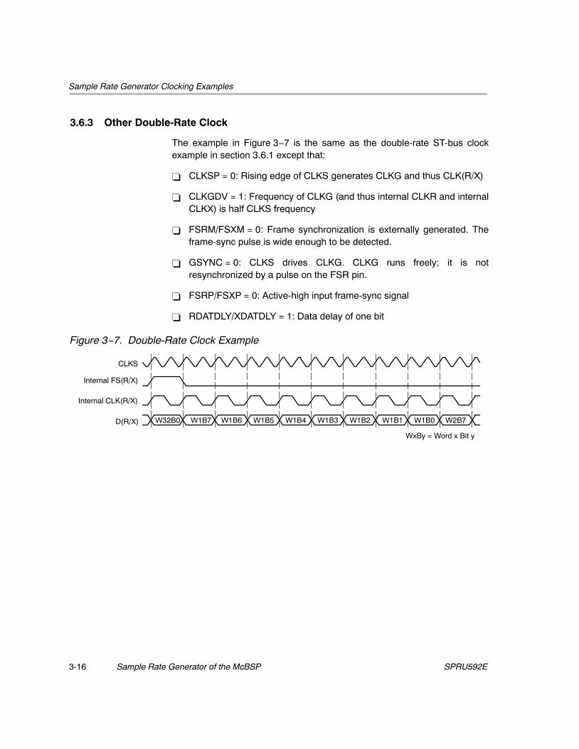
Sample Rate Generator Clocking Examples
Sample Rate Generator of the McBSP3-16 SPRU592E
3.6.3 Other Double-Rate Clock
The example in Figure 3−7 is the same as the double-rate ST-bus clockexample in section 3.6.1 except that:
� CLKSP = 0: Rising edge of CLKS generates CLKG and thus CLK(R/X)
� CLKGDV = 1: Frequency of CLKG (and thus internal CLKR and internalCLKX) is half CLKS frequency
� FSRM/FSXM = 0: Frame synchronization is externally generated. Theframe-sync pulse is wide enough to be detected.
� GSYNC = 0: CLKS drives CLKG. CLKG runs freely; it is notresynchronized by a pulse on the FSR pin.
� FSRP/FSXP = 0: Active-high input frame-sync signal
� RDATDLY/XDATDLY = 1: Data delay of one bit
Figure 3−7. Double-Rate Clock Example
D(R/X)
Internal CLK(R/X)
Internal FS(R/X)
CLKS
WxBy = Word x Bit y
W2B7W1B0W1B1W1B2W1B3W1B4W1B5W1B6W1B7W32B0

4-1
McBSP Exception/Error Conditions
This chapter provides a detailed explanation and listing of exception or errorconditions associated with the McBSP.
Topic Page
4.1 McBSP Exception/Error Conditions 4-2. . . . . . . . . . . . . . . . . . . . . . . . . . . . .
4.2 Overrun in the Receiver 4-3. . . . . . . . . . . . . . . . . . . . . . . . . . . . . . . . . . . . . . .
4.3 Unexpected Receive Frame-Sync Pulse 4-5. . . . . . . . . . . . . . . . . . . . . . . . .
4.4 Overwrite in the Transmitter 4-8. . . . . . . . . . . . . . . . . . . . . . . . . . . . . . . . . . .
4.5 Underflow in the Transmitter 4-9. . . . . . . . . . . . . . . . . . . . . . . . . . . . . . . . . . .
4.6 Unexpected Transmit Frame-Sync Pulse 4-11. . . . . . . . . . . . . . . . . . . . . . .
Chapter 4
McBSP Exception/Error Conditions
McBSP Exception/Error Conditions4-2 SPRU592E
4.1 McBSP Exception/Error Conditions
There are five serial port events that may constitute a system error:
� Receiver Overrun (RFULL = 1 in SPCR1). This occurs when DRR1 hasnot been read since the last RBR-to-DRR copy. Consequently, thereceiver does not copy a new word from the RBR(s) to the DRR(s), andthe RSR(s) are now full with another new word shifted in from DR.Therefore, RFULL = 1 indicates an error condition wherein any new datathat may arrive at this time on DR replaces the contents of the RSR(s), andas a result, the previous word is lost. The RSR(s) continue to beoverwritten as long as new data arrives on DR and DRR1 is not read.
� Unexpected Receive Frame-Sync Pulse (RSYNCERR = 1 in SPCR1).This occurs during reception when RFIG = 0 and an unexpectedframe-sync pulse occurs. An unexpected frame-sync pulse is one thatbegins the next frame transfer before all the bits of the current frame havebeen received. Such a pulse causes data reception to abort and restart.If new data has been copied into the RBR(s) from the RSR(s) since the lastRBR-to-DRR copy, this new data in the RBR(s) is lost. This is because noRBR-to-DRR copy occurs; the reception has been restarted.
� Transmitter Data Overwrite. This occurs when the CPU or the DMAcontroller overwrites data in the DXR(s) before the data is copied to theXSR(s). The overwritten data never reaches the DX pin.
� Transmitter Underflow (XEMPTY = 0 in SPCR2). If a new frame-syncsignal arrives before new data is loaded into DXR1, the previous data inthe DXR(s) is sent again. This will continue for every new frame-syncpulse that arrives until DXR1 is loaded with new data.
� Unexpected Transmit Frame-Synch Pulse (XSYNCERR = 1 inSPCR2). This occurs during transmission when XFIG = 0 and anunexpected frame-sync pulse occurs. An unexpected frame-sync pulse isone that begins the next frame transfer before all the bits of the currentframe have been transferred. Such a pulse causes the current datatransmission to abort and restart. If new data has been written to theDXR(s) since the last DXR-to-XSR copy, the current value in the XSR(s)is lost.

Overrun in the Receiver
4-3McBSP Exception/Error ConditionsSPRU592E
4.2 Overrun in the Receiver
RFULL = 1 in SPCR1 indicates that the receiver has experienced overrun andis in an error condition. RFULL is set when all of the following conditions aremet:
1) DRR1 has not been read since the last RBR-to-DRR copy (RRDY = 1).
2) RBR1 is full and an RBR-to-DRR copy has not occurred.
3) RSR1 is full and an RSR1-to-RBR copy has not occurred.
As described in section 2.5, McBSP Reception, data arriving on DR iscontinuously shifted into RSR1 (for word length of 16 bits or smaller) or RSR2and RSR1 (for word length larger than 16 bits). Once a complete word isshifted into the RSR(s), an RSR-to-RBR copy can occur only if the previousdata in RBR1 has been copied to DRR1. The RRDY bit is set when new dataarrives in DRR1 and is cleared when that data is read from DRR1. UntilRRDY = 0, the next RBR-to-DRR copy will not take place, and the data is heldin the RSR(s). New data arriving on the DR pin is shifted into RSR(s), and theprevious content of the RSR(s) is lost.
You can prevent the loss of data if DRR1 is read no later than 2.5 cycles beforethe end of the third word is shifted into the RSR1.
Important: If both DRRs are needed (word length larger than 16 bits), the CPUor the DMA controller must read from DRR2 first and then from DRR1. As soonas DRR1 is read, the next RBR-to-DRR copy is initiated. If DRR2 is not readfirst, the data in DRR2 is lost.
Note that after the receiver starts running from reset, a minimum of three wordsmust be received before RFULL is set. Either of the following events clears theRFULL bit and allows subsequent transfers to be read properly:
� The CPU or the DMA controller reads DRR1.
� The receiver is reset individually (RRST = 0) or as part of a DSP reset.
Another frame-sync pulse is required to restart the receiver.
4.2.1 Example of the Overrun Condition
Figure 4−1 shows the receive overrun condition. Because serial word A is notread from DRR1 before serial word B arrives in RBR1, B is not transferred toDRR1 yet. Another new word (C) arrives and RSR1 is full with this data. DRR1is finally read, but not earlier than 2.5 cycles before the end of word C.Therefore, new data (D) overwrites word C in RSR1. If DRR1 is not read intime, the next word can overwrite D.

Overrun in the Receiver
McBSP Exception/Error Conditions4-4 SPRU592E
Figure 4−1. Overrun in the McBSP Receiver
No RSR1 to RBR1 copy(C)
No read from DRR1(A)No RBR1 to DRR1 copy(B)No read from DRR1(A)
RBR1 to DRR1 copy(A)
D7C0C1C2C3C4C5C6C7B0B1B2B3B4B5B6B7A0A1
RFULL
RRDY
DR
FSR
CLKR
ÁÁ
ÁÁ
ÁÁ
ÁÁÁÁ
ÁÁ
ÁÁ
4.2.2 Example of Preventing the Overrun Condition
Figure 4−2 shows the case where the overrun condition is prevented by a readfrom DRR1 at least 2.5 cycles before the next serial word (C) is completelyshifted into RSR1. This ensures that an RBR1-to-DRR1 copy of word B occursbefore receiver attempts to transfer word C from RSR1 to RBR1.
Figure 4−2. Overrun Prevented in the McBSP Receiver
RBR1 to DRR1(B)
No RBR1 to DRR1 copy(B)No read from DRR1(A)
RBR1 to DRR1 copy(A)
C0C1C2C3C4C5C6C7B0B1B2B3B4B5B6B7A0A1
RFULL
RRDY
DR
FSR
CLKR
ÁÁÁÁ
ÁÁÁÁ
ÁÁ
Read from DRR1(A)
Latest time to read Afrom DRR1 to prevent
an overrun condition
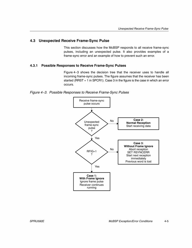
Unexpected Receive Frame-Sync Pulse
4-5McBSP Exception/Error ConditionsSPRU592E
4.3 Unexpected Receive Frame-Sync Pulse
This section discusses how the McBSP responds to all receive frame-syncpulses, including an unexpected pulse. It also provides examples of aframe-sync error and an example of how to prevent such an error.
4.3.1 Possible Responses to Receive Frame-Sync Pulses
Figure 4−3 shows the decision tree that the receiver uses to handle allincoming frame-sync pulses. The figure assumes that the receiver has beenstarted (RRST = 1 in SPCR1). Case 3 in the figure is the case in which an erroroccurs.
Figure 4−3. Possible Responses to Receive Frame-Sync Pulses
Yes
No
Yes
No
ÁÁÁÁÁÁÁÁÁÁÁÁÁÁÁÁÁÁÁÁÁÁÁÁÁÁÁÁÁÁÁÁÁÁÁÁÁÁÁÁ
runningReceiver continuesIgnore frame pulseWith Frame Ignore
Case 1:
ÁÁÁÁÁÁÁÁÁÁÁÁÁÁÁÁÁÁÁÁÁÁÁÁÁÁÁÁÁÁÁÁÁÁÁÁÁÁÁÁÁÁÁÁÁÁÁÁÁÁÁÁÁÁ
Previous word is lostimmediately
Start next receptionSET RSYNCERR
Abort receptionWithout Frame Ignore
Case 3:
ÁÁÁÁÁÁÁÁÁÁÁÁÁÁÁÁÁÁÁÁÁÁÁÁÁÁÁÁÁÁÁÁÁÁÁÁ
Start receiving dataNormal Reception
Case 2:
ÁÁÁÁÁÁÁÁÁÁÁÁÁÁÁÁÁÁÁÁÁÁÁÁ
pulse occursReceive frame-sync
?RFIG=1
ÁÁÁÁÁÁÁÁÁÁÁÁÁÁÁÁÁÁÁÁÁÁÁÁÁÁÁÁÁÁÁÁÁÁÁÁÁÁÁÁÁÁÁÁÁÁÁÁ
?pulse
frame-syncUnexpected

Unexpected Receive Frame-Sync Pulse
McBSP Exception/Error Conditions4-6 SPRU592E
Any one of three cases can occur:
� Case 1: Unexpected internal FSR pulses with RFIG = 1 in RCR2. Receiveframe-sync pulses are ignored, and the reception continues.
� Case 2: Normal serial port reception. Reception continues normallybecause the frame-sync pulse is not unexpected. There are three possiblereasons why a receive operation might not be in progress when the pulseoccurs:
� The FSR pulse is the first pulse after the receiver is enabled(RRST = 1 in SPCR1).
� The FSR pulse is the first pulse after DRR[1,2] is read, clearing areceiver full (RFULL = 1 in SPCR1) condition.
� The serial port is in the interpacket intervals. The programmed datadelay for reception (programmed with the RDATDLY bits in RCR2)may start during these interpacket intervals for the first bit of the nextword to be received. Thus, at maximum frame frequency, framesynchronization can still be received 0 to 2 clock cycles before the firstbit of the synchronized frame.
� Case 3: Unexpected receive frame synchronization with RFIG = 0(frame-sync pulses not ignored). Unexpected frame-sync pulses canoriginate from an external source or from the internal sample rategenerator.
If a frame-sync pulse starts the transfer of a new frame before the currentframe is fully received, this pulse is treated as an unexpected frame-syncpulse, and the receiver sets the receive frame-sync error bit (RSYNCERR)in SPCR1. RSYNCERR can be cleared only by a receiver reset or by awrite of 0 to this bit.
If you want the McBSP to notify the CPU of receive frame-sync errors, youcan set a special receive interrupt mode with the RINTM bits of SPCR1.When RINTM = 11b, the McBSP sends a receive interrupt (RINT) requestto the CPU each time that RSYNCERR is set.
4.3.2 Example of an Unexpected Receive Frame-Sync Pulse
Figure 4−4 shows an unexpected receive frame-sync pulse during normaloperation of the serial port, with time intervals between data packets. Whenthe unexpected frame-sync pulse occurs, the RSYNCERR bit is set, thereception of data B is aborted, and the reception of data C begins. In addition,if RINTM = 11b, the McBSP sends a receive interrupt (RINT) request to theCPU.

Unexpected Receive Frame-Sync Pulse
4-7McBSP Exception/Error ConditionsSPRU592E
Figure 4−4. An Unexpected Frame-Sync Pulse During a McBSP Reception
ÁÁ
ÁÁ
ÁÁ
Unexpected frame synchronization
RBR1 to DRR1(B)
Read from DRR1(C)RBR1 to DRR1 copy(C)Read from DRR1(A)RBR1 to DRR1 copy(A)
C0C1C2C3C4C5C6C7B4B5B6B7A0A1
RSYNCERR
RRDY
DR
FSR
CLKR
4.3.3 Preventing Unexpected Receive Frame-Sync Pulses
Each frame transfer can be delayed by 0, 1, or 2 CLKR cycles, depending onthe value in the RDATDLY bits of RCR2. For each possible data delay,Figure 4−5 shows when a new frame-sync pulse on FSR can safely occurrelative to the last bit of the current frame.
Figure 4−5. Proper Positioning of Frame-Sync PulsesFor 2-bit delay:Next frame-sync pulsehere or later is OK.
For 1-bit delay:Next frame-sync pulsehere or later is OK.
For 0-bit delay:Next frame-sync pulsehere or later is OK.
CLKR/CLKX
FSR/FSX
DR/DX
Last bit ofcurrent frame
Earliest possibletime to begin transferof next frame
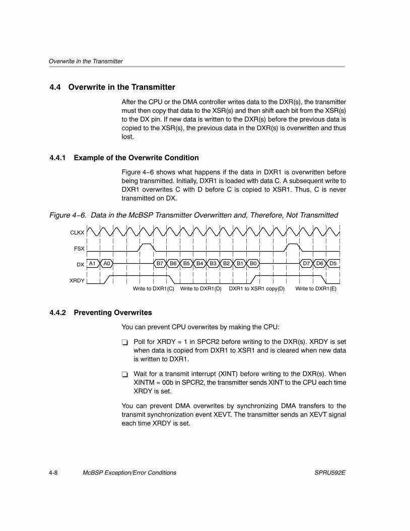
Overwrite in the Transmitter
McBSP Exception/Error Conditions4-8 SPRU592E
4.4 Overwrite in the Transmitter
After the CPU or the DMA controller writes data to the DXR(s), the transmittermust then copy that data to the XSR(s) and then shift each bit from the XSR(s)to the DX pin. If new data is written to the DXR(s) before the previous data iscopied to the XSR(s), the previous data in the DXR(s) is overwritten and thuslost.
4.4.1 Example of the Overwrite Condition
Figure 4−6 shows what happens if the data in DXR1 is overwritten beforebeing transmitted. Initially, DXR1 is loaded with data C. A subsequent write toDXR1 overwrites C with D before C is copied to XSR1. Thus, C is nevertransmitted on DX.
Figure 4−6. Data in the McBSP Transmitter Overwritten and, Therefore, Not Transmitted
Write to DXR1(D)
ÁÁÁÁ
ÁÁ
Write to DXR1(E)DXR1 to XSR1 copy(D)Write to DXR1(C)
D5D6D7B0B1B2B3B4B5B6B7A0A1
XRDY
DX
FSX
CLKX
ÁÁÁÁ
ÁÁÁÁ
4.4.2 Preventing Overwrites
You can prevent CPU overwrites by making the CPU:
� Poll for XRDY = 1 in SPCR2 before writing to the DXR(s). XRDY is setwhen data is copied from DXR1 to XSR1 and is cleared when new datais written to DXR1.
� Wait for a transmit interrupt (XINT) before writing to the DXR(s). WhenXINTM = 00b in SPCR2, the transmitter sends XINT to the CPU each timeXRDY is set.
You can prevent DMA overwrites by synchronizing DMA transfers to thetransmit synchronization event XEVT. The transmitter sends an XEVT signaleach time XRDY is set.

Underflow in the Transmitter
4-9McBSP Exception/Error ConditionsSPRU592E
4.5 Underflow in the Transmitter
The McBSP indicates a transmitter empty (or underflow) condition by clearingthe XEMPTY bit in SPCR2. Either of the following events activates XEMPTY(XEMPTY = 0):
� DXR1 has not been loaded since the last DXR-to-XSR copy, and all bitsof the data word in the XSR(s) have been shifted out on the DX pin.
� The transmitter is reset (by forcing XRST = 0 in SPCR2, or by a DSP reset)and is then restarted.
In the underflow condition, the transmitter continues to transmit the old datathat is in the DXR(s) for every new transmit frame-sync signal until a new valueis loaded into DXR1 by the CPU or the DMA controller.
Note:
If both DXRs are needed (word length larger than 16 bits), the CPU or theDMA controller must load DXR2 first and then load DXR1. As soon as DXR1is loaded, the contents of both DXRs are copied to the transmit shift registers(XSRs). If DXR2 is not loaded first, the previous content of DXR2 is passedto the XSR2.
XEMPTY is deactivated (XEMPTY = 1) when a new word in DXR1 istransferred to XSR1. If FSXM = 1 in PCR and FSGM = 0 in SRGR2, thetransmitter generates a single internal FSX pulse in response to aDXR-to-XSR copy. Otherwise, the transmitter waits for the next frame-syncpulse before sending out the next frame on DX.
When the transmitter is taken out of reset (XRST = 1), it is in a transmitterready (XRDY = 1 in SPCR2) and transmitter empty (XEMPTY = 0) state. IfDXR1 is loaded by the CPU or the DMA controller before internal FSX goesactive high, a valid DXR-to-XSR transfer occurs. This allows for the first wordof the first frame to be valid even before the transmit frame-sync pulse isgenerated or detected. Alternatively, if a transmit frame-sync pulse is detectedbefore DXR1 is loaded, zeros will be output on DX.

Underflow in the Transmitter
McBSP Exception/Error Conditions4-10 SPRU592E
4.5.1 Example of the Underflow Condition
Figure 4−7 shows an underflow condition. After B is transmitted, DXR1 is notreloaded before the subsequent frame-sync pulse. Thus, B is againtransmitted on DX.
Figure 4−7. Underflow During McBSP Transmission
XEMPTY
Á Á B5B6B7B0B1B2B3B4B5B6B7A0A1
XRDY
DX
FSX
CLKX
ÁÁÁÁ
Write to DXR1(C)DXR1 to XSR1 copy(B)
4.5.2 Example of Preventing the Underflow Condition
Figure 4−8 shows the case of writing to DXR1 just before an underflowcondition would otherwise occur. After B is transmitted, C is written to DXR1before the next frame-sync pulse. As a result, there is no underflow; B is nottransmitted twice.
Figure 4−8. Underflow Prevented in the McBSP Transmitter
XEMPTY
ÁÁ
ÁÁ
C5C6C7B0B1B2B3B4B5B6B7A0A1
XRDY
DX
FSX
CLKX
ÁÁ
ÁÁ
DXR1 to XSR1 copy(C)Write to DXR1(C)DXR1 to XSR1 copy

Unexpected Transmit Frame-Sync Pulse
4-11McBSP Exception/Error ConditionsSPRU592E
4.6 Unexpected Transmit Frame-Sync Pulse
This section discusses how the McBSP responds to any transmit frame-syncpulses, including an unexpected pulse. It also provides examples of aframe-sync error and an example of how to prevent such an error.
4.6.1 Possible Responses to Transmit Frame-Sync Pulses
Figure 4−9 shows the decision tree that the transmitter uses to handle allincoming frame-sync pulses. The figure assumes that the transmitter hasbeen started (XRST = 1 in SPCR2). Case 3 in the figure is the case in whichan error occurs.
Figure 4−9. Possible Responses to Transmit Frame-Sync Pulses
Yes
No
Yes
No
runningTransmit stays
Ignore frame pulseWith Frame Ignore
Case 1:
transferRestart current
Set XSYNCERR.Abort transfer.
Without Frame IgnoreCase 3:
Start new transmitNormal Transmission
Case 2:
pulse occursTransmit frame-sync
?XFIG=1
?pulse
frame-syncUnexpected

Unexpected Transmit Frame-Sync Pulse
McBSP Exception/Error Conditions4-12 SPRU592E
Any one of three cases can occur:
� Case 1: Unexpected internal FSX pulses with XFIG = 1 in XCR2.Unexpected transmit frame-sync pulses are ignored, and thetransmission continues.
� Case 2: Normal serial port transmission. Transmission continuesnormally because the frame-sync pulse is not unexpected. There are twopossible reasons why a transmit operations might not be in progress whenthe pulse occurs:
� This FSX pulse is the first after the transmitter is enabled (XRST = 1).
� The serial port is in the interpacket intervals. The programmed datadelay for transmission (programmed with the XDATDLY bits of XCR2)may start during these interpacket intervals before the first bit of theprevious word is transmitted. Therefore, at maximum packetfrequency, frame synchronization can still be received 0 to 2 clockcycles before the first bit of the synchronized frame.
� Case 3: Unexpected transmit frame synchronization with XFIG = 0(frame-sync pulses not ignored). Unexpected frame-sync pulses canoriginate from an external source or from the internal sample rategenerator.
If a frame-sync pulse starts the transfer of a new frame before the currentframe is fully transmitted, this pulse is treated as an unexpectedframe-sync pulse, and the transmitter sets the transmit frame-sync errorbit (XSYNCERR) in SPCR2. XSYNCERR can be cleared only by atransmitter reset or by a write of 0 to this bit.
If you want the McBSP to notify the CPU of frame-sync errors, you can seta special transmit interrupt mode with the XINTM bits of SPCR2. WhenXINTM = 11b, the McBSP sends a transmit interrupt (XINT) request to theCPU each time that XSYNCERR is set.
4.6.2 Example of an Unexpected Transmit Frame-Sync Pulse
Figure 4−10 shows an unexpected transmit frame-sync pulse during normaloperation of the serial port, with intervals between the data packets. When theunexpected frame-sync pulse occurs, the XSYNCERR bit is set and becauseno new data has been passed to XSR1 yet, the transmission of data B isrestarted. In addition, if XINTM = 11b, the McBSP sends a transmit interrupt(XINT) request to the CPU.

Unexpected Transmit Frame-Sync Pulse
4-13McBSP Exception/Error ConditionsSPRU592E
Figure 4−10. An Unexpected Frame-Sync Pulse During a McBSP Transmission
ÁÁ
B0B1B2B3B4B5B6B7B4B5B6B7A0A1
XSYNCERR
XRDY
DX
FSX
CLKX
ÁÁ
ÁÁ
Write to DXR1(D)DXR1 to XSR1 (C)Write to DXR1(C)DXR1 to XSR1 copy(B)
Unexpected frame synchronization
4.6.3 Preventing Unexpected Transmit Frame-Sync Pulses
Each frame transfer can be delayed by 0, 1, or 2 CLKX cycles, depending onthe value in the XDATDLY bits of XCR2. For each possible data delay,Figure 4−11 shows when a new frame-sync pulse on FSX can safely occurrelative to the last bit of the current frame.
Figure 4−11.Proper Positioning of Frame-Sync Pulses
For 2-bit delay:Next frame-sync pulsehere or later is OK.
For 1-bit delay:Next frame-sync pulsehere or later is OK.
For 0-bit delay:Next frame-sync pulsehere or later is OK.
CLKR/CLKX
FSR/FSX
DR/DX
Last bit ofcurrent frame
Earliest possibletime to begin transferof next frame

Unexpected Transmit Frame-Sync Pulse
McBSP Exception/Error Conditions4-14 SPRU592E
This page is intentionally left blank.

5-1
Multichannel Selection Modes
This chapter defines and provides the functions and all related informationconcerning the multichannel selection modes.
Topic Page
5.1 Channels, Blocks, and Partitions 5-2. . . . . . . . . . . . . . . . . . . . . . . . . . . . . . .
5.2 Multichannel Selection 5-3. . . . . . . . . . . . . . . . . . . . . . . . . . . . . . . . . . . . . . . .
5.3 Configuring a Frame for Multichannel Selection 5-4. . . . . . . . . . . . . . . . .
5.4 Using Two Partitions 5-5. . . . . . . . . . . . . . . . . . . . . . . . . . . . . . . . . . . . . . . . . .
5.5 Using Eight Partitions 5-8. . . . . . . . . . . . . . . . . . . . . . . . . . . . . . . . . . . . . . . . .
5.6 Receive Multichannel Selection Mode 5-10. . . . . . . . . . . . . . . . . . . . . . . . .
5.7 Transmit Multichannel Selection Mode 5-11. . . . . . . . . . . . . . . . . . . . . . . . .
5.8 Using Interrupts Between Block Transfers 5-15. . . . . . . . . . . . . . . . . . . . .
Chapter 5
Channels, Blocks, and Partitions
Multichannel Selection Modes5-2 SPRU592E
5.1 Channels, Blocks, and Partitions
A McBSP channel is a time slot for shifting in/out the bits of one serial word.Each McBSP supports up to 128 channels for reception and 128 channels fortransmission.
In the receiver and in the transmitter, the 128 available channels are dividedinto eight blocks that each contain 16 contiguous channels:
Block 0: Channels 0–15Block 1: Channels 16–31Block 2: Channels 32–47Block 3: Channels 48–63
Block 4: Channels 64–79Block 5: Channels 80–95Block 6: Channels 96–111Block 7: Channels 112–127
The blocks are assigned to partitions according to the selected partitionmode. In the 2-partition mode, you assign one even-numbered block (0, 2, 4,or 6) to partition A and one odd-numbered block (1, 3, 5, or 7) to partition B.In the 8-partition mode, blocks 0 through 7 are automatically assigned topartitions, A through H, respectively.
The number of partitions for reception and the number of partitions fortransmission are independent. For example, it is possible to use 2 receivepartitions (A and B) and 8 transmit partitions (A–H).

Multichannel Selection
5-3Multichannel Selection ModesSPRU592E
5.2 Multichannel Selection
When a McBSP uses a time-division multiplexed (TDM) data stream whilecommunicating with other McBSPs or serial devices, the McBSP may need toreceive and/or transmit on only a few channels. To save memory and busbandwidth, you can use a multichannel selection mode to prevent data flowin some of the channels. The McBSP has one receive multichannel selectionmode and three transmit multichannel selection modes.
Each channel partition has a dedicated channel enable register. If theappropriate multichannel selection mode is on, each bit in the register controlswhether data flow is allowed or prevented in one of the channels that isassigned to that partition.

Configuring a Frame for Multichannel Selection
Multichannel Selection Modes5-4 SPRU592E
5.3 Configuring a Frame for Multichannel Selection
Before you enable a multichannel selection mode, make sure you properlyconfigure the data frame:
� Select a single-phase frame (RPHASE/XPHASE = 0). Each framerepresents a TDM data stream.
� Set a frame length (in RFRLEN1/XFRLEN1) that includes thehighest-numbered channel that is to be used. For example, if you plan touse channels 0, 15, and 39 for reception, the receive frame length mustbe at least 40 (RFRLEN1 = 39). If XFRLEN1 = 39 in this case, the receivercreates 40 time slots per frame but only receives data during time slots 0,15, and 39 of each frame.
Note:
The frame-sync pulse can be generated internally by the sample rate gener-ator or it can be supplied externally by another source. In a multichannelmode configuration with external frame-sync generation, theTMS320VC5501/02 McBSP transmitter will ignore the first frame-sync pulseafter it is taken out of reset. The transmitter will transmit only on the secondframe-sync pulse. The receiver will shift in data on the first frame-sync pulseregardless of whether it is generated internally or externally.

Using Two Partitions
5-5Multichannel Selection ModesSPRU592E
5.4 Using Two Partitions
For multichannel selection operation in the receiver and/or the transmitter, youcan use two partitions or eight partitions. If you choose the 2-partition mode(RMCME = 0 for reception, XMCME = 0 for transmission), McBSP channelsare activated using an alternating scheme. In response to a frame-sync pulse,the receiver or transmitter begins with the channels in partition A and thenalternates between partitions B and A until the complete frame has beentransferred. When the next frame-sync pulse occurs, the next frame istransferred, beginning with the channels in partition A.
5.4.1 Assigning Blocks to Partitions A and B
For reception, any two of the eight receive-channel blocks can be assigned toreceive partitions A and B, which means up to 32 receive channels can beenabled at any given point in time. Similarly, any two of the eighttransmit-channel blocks (up 32 enabled transmit channels) can be assignedto transmit partitions A and B.
For reception:
� Assign an even-numbered channel block (0, 2, 4, or 6) to receive partitionA by writing to the RPABLK bits. In the receive multichannel selectionmode, the channels in this partition are controlled by receive channelenable register A (RCERA).
� Assign an odd-numbered block (1, 3, 5, or 7) to receive partition B with theRPBBLK bits. In the receive multichannel selection mode, the channelsin this partition are controlled by receive channel enable register B(RCERB).
For transmission:
� Assign an even-numbered channel block (0, 2, 4, or 6) to transmit partitionA by writing to the XPABLK bits. In one of the transmit multichannelselection modes, the channels in this partition are controlled by transmitchannel enable register A (XCERA).
� Assign an odd-numbered block (1, 3, 5, or 7) to transmit partition B withthe XPBBLK bits. In one of the transmit multichannel selection modes, thechannels in this partition are controlled by transmit channel enable registerB (XCERB).

Using Two Partitions
Multichannel Selection Modes5-6 SPRU592E
Figure 5−1 shows an example of alternating between the channels of partitionA and the channels of partition B. Channels 0-15 have been assigned topartition A, and channels 16-31 have been assigned to partition B. In responseto a frame-sync pulse, the McBSP begins a frame transfer with partition A andthen alternates between partitions B and A until the complete frame istransferred.
Figure 5−1. Alternating Between the Channels of Partition A and the Channels ofPartition B
0-1516-310-1516-310-1516-310-1516-310-15
Block
Channels
FS(R/X)ÁÁÁÁÁÁÁÁÁÁÁÁÁÁÁÁÁÁÁÁÁÁÁÁÁÁÁÁÁÁÁÁÁÁÁÁÁÁÁÁÁÁÁÁÁÁÁÁÁÁ
0 1 0 1 0 1 0 1 0
Partition A B A B A B A B A
2-partition mode. Example with fixed block assignments
As explained next, you can dynamically change which blocks of channels areassigned to the partitions.
5.4.2 Reassigning Blocks During Reception/Transmission
If you want to use more than 32 channels, you can change which channelblocks are assigned to partitions A and B during the course of a data transfer.However, these changes must be carefully timed. While a partition is beingtransferred, its the associated block assignment bits cannot be modified, andits associated channel enable register cannot be modified. For example, ifblock 3 is being transferred and block 3 is assigned to partition A, you cannotmodify (R/X)PABLK to assign different channels to partition A, and you cannotmodify (R/X)CERA to change the channel configuration for partition A. Severalfeatures of the McBSP help you time the reassignment:
� The block of channels currently involved in reception/transmission (thecurrent block) is reflected in the RCBLK/XCBLK bits. Your program canpoll these bits to determine which partition is active. When a partition is notactive, it is safe to change its block assignment and channel configuration.
� At the end of every block (at the boundary of two partitions), an interruptcan be sent to the CPU. In response to the interrupt, the CPU can thencheck the RCBLK/XCBLK bits and update the inactive partition.
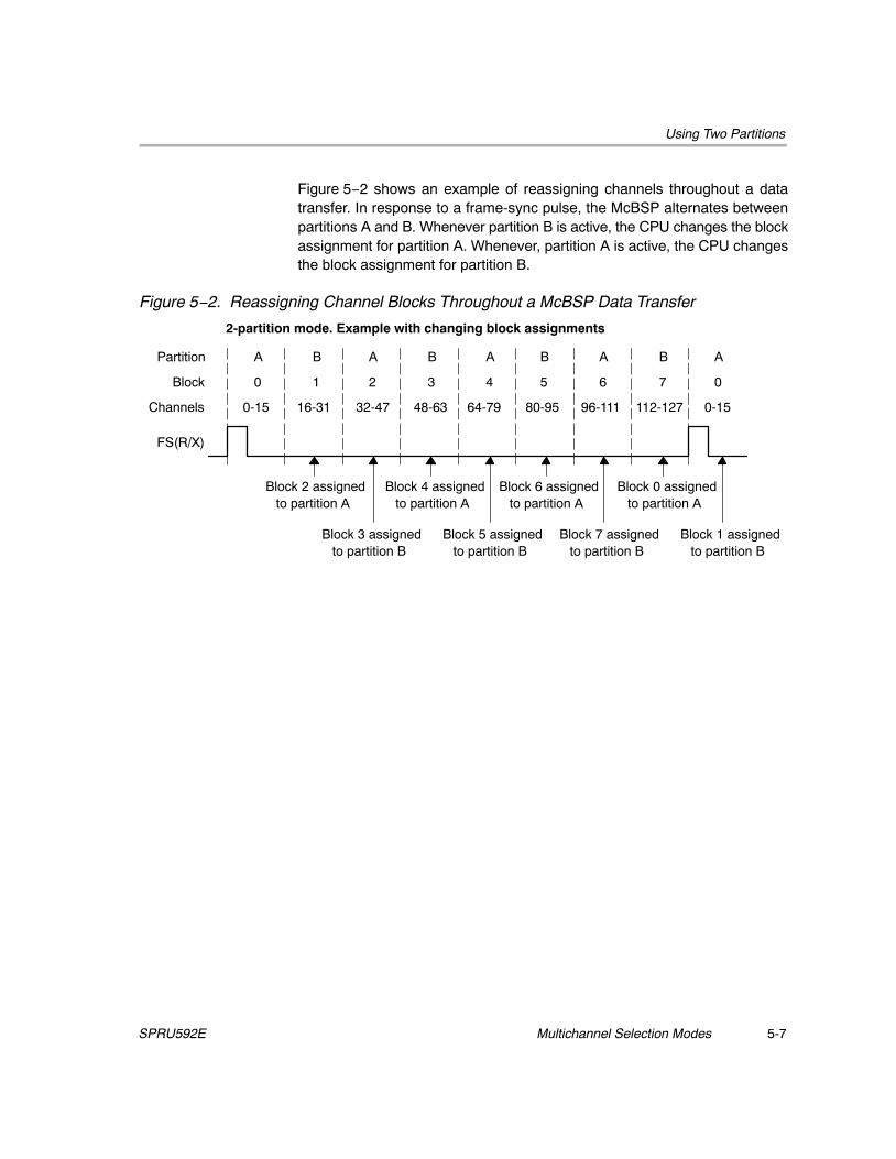
Using Two Partitions
5-7Multichannel Selection ModesSPRU592E
Figure 5−2 shows an example of reassigning channels throughout a datatransfer. In response to a frame-sync pulse, the McBSP alternates betweenpartitions A and B. Whenever partition B is active, the CPU changes the blockassignment for partition A. Whenever, partition A is active, the CPU changesthe block assignment for partition B.
Figure 5−2. Reassigning Channel Blocks Throughout a McBSP Data Transfer
0-15112-12796-11180-9564-7948-6332-4716-310-15
Block
Channels
FS(R/X)ÁÁÁÁÁÁÁÁÁÁÁÁÁÁÁÁÁÁÁÁÁÁÁÁÁÁÁÁÁÁÁÁÁÁÁÁÁÁÁÁÁÁÁÁÁÁÁÁÁÁ
0 1 2 3 4 5 6 7 0
Partition A B A B A B A B A
Block 2 assignedto partition A
Block 4 assignedto partition A
Block 6 assignedto partition A
Block 0 assignedto partition A
Block 3 assignedto partition B
Block 5 assignedto partition B
Block 7 assignedto partition B
Block 1 assignedto partition B
2-partition mode. Example with changing block assignments

Using Eight Partitions
Multichannel Selection Modes5-8 SPRU592E
5.5 Using Eight Partitions
For multichannel selection operation in the receiver and/or the transmitter, youcan use eight partitions or two partitions. If you choose the 8-partition mode(RMCME = 1 for reception, XMCME = 1 for transmission), McBSP partitionsare activated in the following order: A, B, C, D, E, F, G, H. In response to aframe-sync pulse, the receiver or transmitter begins with the channels inpartition A and then continues with the other partitions in order until thecomplete frame has been transferred. When the next frame-sync pulseoccurs, the next frame is transferred, beginning with the channels in partitionA.
In the 8-partition mode, the (R/X)PABLK and (R/X)PBBLK bits are ignored andthe 16-channel blocks are assigned to the partitions as shown in Table 5−1 andTable 5−2. These assignments cannot be changed. The tables also show theregisters used to control the channels in the partitions.
Table 5−1. Receive Channel Assignment and Control When Eight Receive PartitionsAre Used
ReceivePartition
Assigned Block ofReceive Channels
Register Used ForChannel Control
A Block 0: channels 0 through 15 RCERA
B Block 1: channels 16 through 31 RCERB
C Block 2: channels 32 through 47 RCERC
D Block 3: channels 48 through 63 RCERD
E Block 4: channels 64 through 79 RCERE
F Block 5: channels 80 through 95 RCERF
G Block 6: channels 96 through 111 RCERG
H Block 7: channels 112 through 127 RCERH
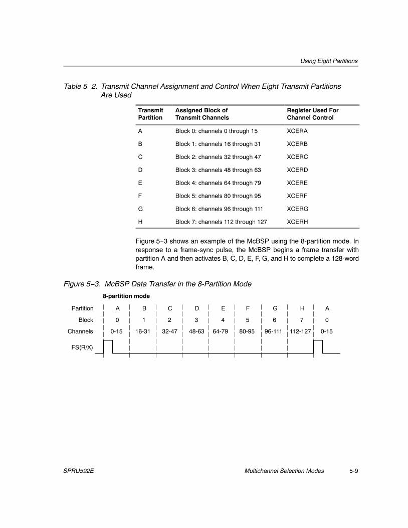
Using Eight Partitions
5-9Multichannel Selection ModesSPRU592E
Table 5−2. Transmit Channel Assignment and Control When Eight Transmit PartitionsAre Used
TransmitPartition
Assigned Block ofTransmit Channels
Register Used ForChannel Control
A Block 0: channels 0 through 15 XCERA
B Block 1: channels 16 through 31 XCERB
C Block 2: channels 32 through 47 XCERC
D Block 3: channels 48 through 63 XCERD
E Block 4: channels 64 through 79 XCERE
F Block 5: channels 80 through 95 XCERF
G Block 6: channels 96 through 111 XCERG
H Block 7: channels 112 through 127 XCERH
Figure 5−3 shows an example of the McBSP using the 8-partition mode. Inresponse to a frame-sync pulse, the McBSP begins a frame transfer withpartition A and then activates B, C, D, E, F, G, and H to complete a 128-wordframe.
Figure 5−3. McBSP Data Transfer in the 8-Partition Mode
0-15112-12796-11180-9564-7948-6332-4716-310-15
Block
Channels
FS(R/X)ÁÁÁÁÁÁÁÁÁÁÁÁÁÁÁÁÁÁÁÁÁÁÁÁÁÁÁÁÁÁÁÁÁÁÁÁÁÁÁÁÁÁÁÁÁÁÁÁÁÁ
0 1 2 3 4 5 6 7 0
Partition A B C D E F G H A
8-partition mode

Receive Multichannel Selection Mode
Multichannel Selection Modes5-10 SPRU592E
5.6 Receive Multichannel Selection Mode
The RMCM bit of MCR1 determines whether all channels or only selectedchannels are enabled for reception. When RMCM = 0, all 128 receivechannels are enabled and cannot be disabled. When RMCM = 1, the receivemultichannel selection mode is enabled. In this mode:
� Channels can be individually enabled or disabled. The only channelsenabled are those selected in the appropriate receive channel enableregisters (RCERs). The way channels are assigned to the RCERsdepends on the number of receive channel partitions (2 or 8), as definedby the RMCME bit of MCR1.
� If a receive channel is disabled, any bits received in that channel arepassed only as far as the receive buffer register(s) (RBR(s)). The receiverdoes not copy the content of the RBR(s) to the DRR(s), and as a result,does not set the receiver ready bit (RRDY). Therefore, no DMAsynchronization event (REVT) is generated, and if the receiver interruptmode depends on RRDY (RINTM = 00b), no interrupt is generated.
As an example of how the McBSP behaves in the receive multichannelselection mode, suppose you enable only channels 0, 15, and 39 and that theframe length is 40. The McBSP:
1) Accepts bits shifted in from the DR pin in channel 0
2) Ignores bits received in channels 1–14
3) Accepts bits shifted in from the DR pin in channel 15
4) Ignores bits received in channels 16–38
5) Accepts bits shifted in from the DR pin in channel 39
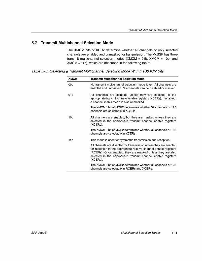
Transmit Multichannel Selection Mode
5-11Multichannel Selection ModesSPRU592E
5.7 Transmit Multichannel Selection Mode
The XMCM bits of XCR2 determine whether all channels or only selectedchannels are enabled and unmasked for transmission. The McBSP has threetransmit multichannel selection modes (XMCM = 01b, XMCM = 10b, andXMCM = 11b), which are described in the following table:
Table 5−3. Selecting a Transmit Multichannel Selection Mode With the XMCM Bits
XMCM Transmit Multichannel Selection Mode
00b No transmit multichannel selection mode is on. All channels areenabled and unmasked. No channels can be disabled or masked.
01b All channels are disabled unless they are selected in theappropriate transmit channel enable registers (XCERs). If enabled,a channel in this mode is also unmasked.
The XMCME bit of MCR2 determines whether 32 channels or 128channels are selectable in XCERs.
10b All channels are enabled, but they are masked unless they areselected in the appropriate transmit channel enable registers(XCERs).
The XMCME bit of MCR2 determines whether 32 channels or 128channels are selectable in XCERs.
11b This mode is used for symmetric transmission and reception.
All channels are disabled for transmission unless they are enabledfor reception in the appropriate receive channel enable registers(RCERs). Once enabled, they are masked unless they are alsoselected in the appropriate transmit channel enable registers(XCERs).
The XMCME bit of MCR2 determines whether 32 channels or 128channels are selectable in RCERs and XCERs.
Transmit Multichannel Selection Mode
Multichannel Selection Modes5-12 SPRU592E
As an example of how the McBSP behaves in a transmit multichannelselection mode, suppose that XMCM = 01b (all channels disabled unlessindividually enabled) and that you have enabled only channels 0, 15, and 39.Suppose also that the frame length is 40. The McBSP…
1) Shifts data to the DX pin in channel 0
2) Places the DX pin in the high-impedance state in channels 1–14
3) Shifts data to the DX pin in channel 15
4) Places the DX pin in the high-impedance state in channels 16–38
5) Shifts data to the DX pin in channel 39
5.7.1 Disabling/Enabling Versus Masking/Unmasking
For transmission, a channel can be:
� Enabled and unmasked (transmission can begin and can be completed)
� Enabled but masked (transmission can begin but cannot be completed)
� Disabled (transmission cannot occur)
The following definitions explain the channel control options:
Enabled channel A channel that can begin transmission by passingdata from the data transmit register(s) (DXR(s)) tothe transmit shift registers (XSR(s)).
Masked channel A channel that cannot complete transmission. TheDX pin is held in the high-impedance state; datacannot be shifted out on the DX pin.
In systems where symmetric transmit and receiveprovides software benefits, this feature allowstransmit channels to be disabled on a shared serialbus. A similar feature is not needed for receptionbecause multiple receptions cannot cause serial buscontention.
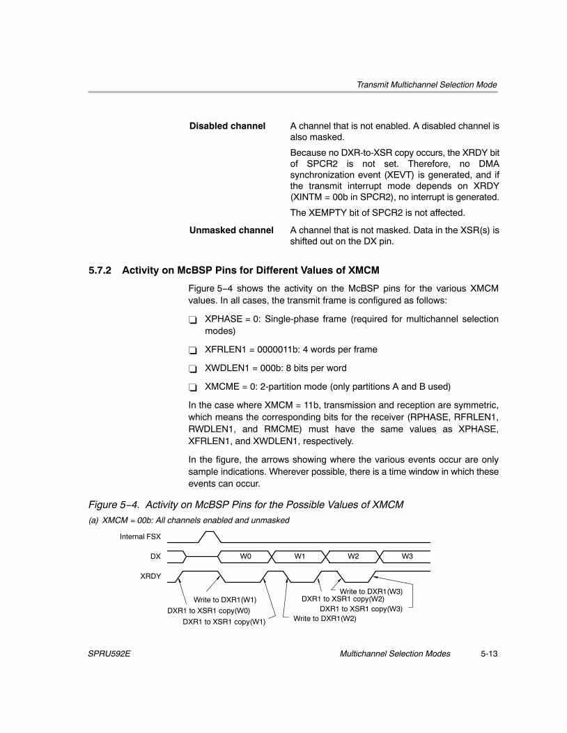
Transmit Multichannel Selection Mode
5-13Multichannel Selection ModesSPRU592E
Disabled channel A channel that is not enabled. A disabled channel isalso masked.
Because no DXR-to-XSR copy occurs, the XRDY bitof SPCR2 is not set. Therefore, no DMAsynchronization event (XEVT) is generated, and ifthe transmit interrupt mode depends on XRDY(XINTM = 00b in SPCR2), no interrupt is generated.
The XEMPTY bit of SPCR2 is not affected.
Unmasked channel A channel that is not masked. Data in the XSR(s) isshifted out on the DX pin.
5.7.2 Activity on McBSP Pins for Different Values of XMCM
Figure 5−4 shows the activity on the McBSP pins for the various XMCMvalues. In all cases, the transmit frame is configured as follows:
� XPHASE = 0: Single-phase frame (required for multichannel selectionmodes)
� XFRLEN1 = 0000011b: 4 words per frame
� XWDLEN1 = 000b: 8 bits per word
� XMCME = 0: 2-partition mode (only partitions A and B used)
In the case where XMCM = 11b, transmission and reception are symmetric,which means the corresponding bits for the receiver (RPHASE, RFRLEN1,RWDLEN1, and RMCME) must have the same values as XPHASE,XFRLEN1, and XWDLEN1, respectively.
In the figure, the arrows showing where the various events occur are onlysample indications. Wherever possible, there is a time window in which theseevents can occur.
Figure 5−4. Activity on McBSP Pins for the Possible Values of XMCM
(a) XMCM = 00b: All channels enabled and unmasked
W3W2W1W0
XRDY
DX
Internal FSX
DXR1 to XSR1 copy(W0)
Write to DXR1(W1)
DXR1 to XSR1 copy(W1) Write to DXR1(W2)DXR1 to XSR1 copy(W3)
DXR1 to XSR1 copy(W2)Write to DXR1(W3)
ÁÁÁÁ
ÁÁ

Transmit Multichannel Selection Mode
Multichannel Selection Modes5-14 SPRU592E
Figure 5−4. Activity on McBSP Pins for the Possible Values of XMCM (Continued)
(b) XMCM = 01b, XPABLK = 00b, XCERA = 000Ah: Only channels 1 and 3 enabled and unmasked
DXR1 to XSR1 copy(W3)Write to DXR1(W3)
XRDY
DXR1 to XSR1 copy(W1)
W3ÁÁ
ÁÁ
ÁÁ
DXÁÁ W1
Internal FSX
(c) XMCM = 10b, XPABLK = 00b, XCERA = 000Ah: All channels enabled, only 1 and 3 unmasked
ÁÁÁÁ
Write to DXR1(W3)
DXR1 to XSR1 copy(W0)
Write to DXR1(W1)
DXR1 to XSR1 copy(W1) Write to DXR1(W2)
XRDY
DXR1 to XSR1 copy(W3)DXR1 to XSR1 copy(W2)
W3
Internal FSX
ÁÁ
ÁÁW1
ÁÁ
ÁÁDX
(d) XMCM = 11b, RPABLK = 00b, XPABLK = X, RCERA = 000Ah, XCERA = 0008h:Receive channels: 1 and 3 enabled; transmit channels: 1 and 3 enabled, but only 3 unmasked
DXR1 to XSR1 copy (W1)
XRDY
DXR1 to XSR1 copy (W3)Write to DXR1(W3)
ÁÁÁÁ
ÁÁ
W3ÁÁ
DX
RBR1 to DRR1 (W3)
Read from DRR1(W1)RBR1 to DRR1 copy (W1)RBR1 to DRR1 copy (W3)
Read from DRR1(W3)
ÁÁÁÁ
W3ÁÁ
ÁÁ
W1ÁÁ
ÁÁ
Internal FS(R/X)
DR
RRDY
Using Interrupts Between Block Transfers
5-15Multichannel Selection ModesSPRU592E
5.8 Using Interrupts Between Block Transfers
When a multichannel selection mode is used, an interrupt request can be sentto the CPU at the end of every 16-channel block (at the boundary betweenpartitions and at the end of the frame). In the receive multichannel selectionmode, a receive interrupt (RINT) request is generated at the end of each blocktransfer if RINTM = 01b. In any of the transmit multichannel selection modes,a transmit interrupt (XINT) request is generated at the end of each blocktransfer if XINTM = 01b. When RINTM/XINTM = 01b, no interrupt isgenerated unless a multichannel selection mode is on.
These interrupt pulses are active high and last for 2 McBSP internal input clockcycles.
This type of interrupt is especially helpful if you are using the 2-partition modeand you want to know when you can assign a different block of channels topartition A or B.

Using Interrupts Between Block Transfers
Multichannel Selection Modes5-16 SPRU592E
This page is intentionally left blank.
6-1
SPI Operation Using the Clock Stop Mode
This chapter describes how the McBSP can communicate with one or moredevices using the SPI protocol.
Topic Page
6.1 SPI Protocol 6-2. . . . . . . . . . . . . . . . . . . . . . . . . . . . . . . . . . . . . . . . . . . . . . . . . .
6.2 Clock Stop Mode 6-3. . . . . . . . . . . . . . . . . . . . . . . . . . . . . . . . . . . . . . . . . . . . . .
6.3 Bits Used to Enable and Configure the Clock Stop Mode 6-4. . . . . . . . .
6.4 Clock Stop Mode Timing Diagrams 6-6. . . . . . . . . . . . . . . . . . . . . . . . . . . . .
6.5 Procedure for Configuring a McBSP for SPI Operation 6-8. . . . . . . . . . .
6.6 McBSP as the SPI Master 6-10. . . . . . . . . . . . . . . . . . . . . . . . . . . . . . . . . . . . .
6.7 McBSP as an SPI Slave 6-13. . . . . . . . . . . . . . . . . . . . . . . . . . . . . . . . . . . . . . .
Chapter 6

SPI Protocol
SPI Operation Using the Clock Stop Mode6-2 SPRU592E
6.1 SPI Protocol
The SPI protocol is a master-slave configuration with one master device andone or more slave devices. The interface consists of the following four signals:
� Serial data input (also referred to as Master In − Slave Out, or MISO)� Serial data output (also referred to as Master Out − Slave In, or MOSI)� Shift-clock (also referred to as SCK)� Slave-enable signal (also referred to as SS)
A typical SPI interface with a single slave device is shown in Figure 6−1.
Figure 6−1. Typical SPI Interface
SPI-compliant
SCK
MOSI
MISO
SS
SPI-compliantslave
SCK
MOSI
MISO
SS
master
The master device controls the flow of communication by providing shift-clockand slave-enable signals. The slave-enable signal is an optional active-lowsignal that enables the serial data input and output of the slave device (thedevice not sending out the clock).
In the absence of a dedicated slave-enable signal, communication betweenthe master and slave is determined by the presence or absence of an activeshift-clock. When the McBSP is operating in SPI master mode and the SSsignal is not used by the slave SPI port, the slave device must remain enabledat all times, and multiple slaves cannot be used.

Clock Stop Mode
6-3SPI Operation Using the Clock Stop ModeSPRU592E
6.2 Clock Stop Mode
The clock stop mode of the McBSP provides compatibility with the SPIprotocol. When the McBSP is configured in clock stop mode, the transmitterand receiver are internally synchronized, so that the McBSP functions as anSPI master or slave device. The transmit clock signal (CLKX) corresponds tothe serial clock signal (SCK) of the SPI protocol, while the transmitframe-synchronization signal (FSX) is used as the slave-enable signal (SS).
The receive clock signal (CLKR) and receive frame-synchronization signal(FSR) are not used in the clock stop mode because these signals are internallyconnected to their transmit counterparts, CLKX and FSX.

Bits Used to Enable and Configure the Clock Stop Mode
SPI Operation Using the Clock Stop Mode6-4 SPRU592E
6.3 Bits Used to Enable and Configure the Clock Stop Mode
The bits required to configure the McBSP as an SPI device are introduced inTable 6−1. Table 6−2 shows how the various combinations of the CLKSTP bitand the polarity bits CLKXP and CLKRP create four possible clock stop modeconfigurations. The timing diagrams in section 6.4 show the effects ofCLKSTP, CLKXP, and CLKRP.
Table 6−1. Bits Used to Enable and Configure the Clock Stop Mode
Bit Field Description
CLKSTP bits of SPCR1 Use these bits to enable the clock stop mode and toselect one of two timing variations.
CLKXP bit of PCR This bit determines the polarity of the CLKX signal.
CLKRP bit of PCR This bit determines the polarity of the CLKR signal.
CLKXM bit of PCR This bit determines whether CLKX is an input signal(McBSP as slave) or an output signal (McBSP asmaster).
XPHASE bit of XCR2 You must use a single-phase transmit frame(XPHASE = 0).
RPHASE bit of RCR2 You must use a single-phase receive frame(RPHASE = 0).
XFRLEN1 bits of XCR1 You must use a transmit frame length of 1 serial word(XFRLEN1 = 0).
RFRLEN1 bits of RCR1 You must use a receive frame length of 1 serial word(RFRLEN1 = 0).
XWDLEN1 bits of XCR1 The XWDLEN1 bits determine the transmit packetlength. XWDLEN1 must be equal to RWDLEN1because in the clock stop mode, the McBSP transmitand receive circuits are synchronized to a single clock.
RWDLEN1 bits of RCR1 The RWDLEN1 bits determine the receive packetlength. RWDLEN1 must be equal to XWDLEN1because in the clock stop mode, the McBSP transmitand receive circuits are synchronized to a single clock.

Bits Used to Enable and Configure the Clock Stop Mode
6-5SPI Operation Using the Clock Stop ModeSPRU592E
Table 6−2. Effects of CLKSTP, CLKXP, and CLKRP on the Clock Scheme
Bit Settings Clock Scheme
CLKSTP = 00b or 01bCLKXP = 0 or 1CLKRP = 0 or 1
Clock stop mode disabled. Clock enabled for non-SPImode.
CLKSTP = 10bCLKXP = 0CLKRP = 0
Low inactive state without delay: The McBSP transmitsdata on the rising edge of CLKX and receives data onthe falling edge of CLKR.
CLKSTP = 11bCLKXP = 0CLKRP = 1
Low inactive state with delay: The McBSP transmitsdata one-half cycle ahead of the rising edge of CLKXand receives data on the rising edge of CLKR.
CLKSTP = 10bCLKXP = 1CLKRP = 0
High inactive state without delay: The McBSP transmitsdata on the falling edge of CLKX and receives data onthe rising edge of CLKR.
CLKSTP = 11bCLKXP = 1CLKRP = 1
High inactive state with delay: The McBSP transmitsdata one-half cycle ahead of the falling edge of CLKXand receives data on the falling edge of CLKR.

Clock Stop Mode Timing Diagrams
SPI Operation Using the Clock Stop Mode6-6 SPRU592E
6.4 Clock Stop Mode Timing Diagrams
The timing diagrams for the four possible clock stop mode configurations areshown here. Notice that the frame-synchronization signal used in clock stopmode is active throughout the entire transmission as a slave-enable signal.Although the timing diagrams show 8-bit transfers, the packet length can beset to 8, 12, 16, 20, 24, or 32 bits per packet. The receive packet length isselected with the RWDLEN1 bits of RCR1, and the transmit packet length isselected with the XWDLEN1 bits of XCR1. For clock stop mode, the values ofRWDLEN1 and XWDLEN1 must be the same because the McBSP transmitand receive circuits are synchronized to a single clock.
Note:
Even if multiple words are consecutively transferred, the CLKX signal isalways stopped and the FSX signal returns to the inactive state after a packettransfer. When consecutive packet transfers are performed, this leads to aminimum idle time of two bit-periods between each packet transfer.
Figure 6−2. SPI Transfer With CLKSTP = 10b (no clock delay), CLKXP = 0, CLKRP = 0
ÁÁ
ÁÁ
ÁÁ
ÁÁ
B1B2B4 B3 B0B5B6B7
B0B1B2B3B4B5B6B7
FSX/SS
DX or DR/MOSI(from master)
CLKX/SCK
ÁÁÁÁÁÁÁÁÁÁÁÁÁÁÁÁÁÁÁÁÁÁÁÁÁÁÁÁÁÁÁÁÁÁÁÁÁÁÁÁÁÁÁÁÁÁ
ÁÁÁÁÁÁÁÁÁÁÁÁÁÁÁÁÁÁÁÁÁÁÁÁÁÁÁÁÁÁÁÁÁÁÁÁÁÁÁÁÁÁÁÁÁÁÁÁ
DX or DR/MISO(from slave)
Notes: 1) If the McBSP is the SPI master (CLKXM = 1), MOSI = DX. If the McBSP is the SPI slave (CLKXM = 0), MOSI = DR.
2) If the McBSP is the SPI master (CLKXM = 1), MISO = DR. If the McBSP is the SPI slave (CLKXM = 0), MISO = DX.
Figure 6−3. SPI Transfer With CLKSTP = 11b (clock delay), CLKXP = 0, CLKRP = 1
ÁÁ
ÁÁ
ÁÁ
ÁÁ
B1B2B4 B3 B0B5B6B7
B0B1B2B3B4B5B6B7
FSX/SS
DX or DR/MOSI(from master)
CLKX/SCK
ÁÁÁÁÁÁÁÁÁÁÁÁÁÁÁÁÁÁÁÁÁÁÁ
ÁÁÁÁÁÁÁÁÁÁÁÁÁÁÁÁÁÁÁÁÁÁÁÁÁÁÁÁÁÁÁÁÁÁÁÁÁÁÁÁÁÁÁÁ
DX or DR/MISO(from slave)
Notes: 1) If the McBSP is the SPI master (CLKXM = 1), MOSI = DX. If the McBSP is the SPI slave (CLKXM = 0), MOSI = DR.
2) If the McBSP is the SPI master (CLKXM = 1), MISO = DR. If the McBSP is the SPI slave (CLKXM = 0), MISO = DX.

Clock Stop Mode Timing Diagrams
6-7SPI Operation Using the Clock Stop ModeSPRU592E
Figure 6−4. SPI Transfer With CLKSTP = 10b (no clock delay), CLKXP = 1, CLKRP = 0
ÁÁ
ÁÁÁÁ
ÁÁ
ÁÁÁÁ
B1B2B4 B3 B0B5B6B7
B0B1B2B3B4B5B6B7
FSX/SS
CLKX/SCK
ÁÁÁÁÁÁÁÁÁÁÁÁÁÁÁÁÁÁÁÁÁÁÁÁÁÁÁÁÁÁÁÁÁÁÁÁÁÁÁÁÁÁÁÁÁÁÁÁ
ÁÁÁÁÁÁÁÁÁÁÁÁÁÁÁÁÁÁÁÁÁÁÁÁÁÁÁÁÁÁÁÁÁÁÁÁÁÁÁÁÁÁÁÁÁÁÁÁ
DX or DR/MOSI(from master)
DX or DR/MISO(from slave)
Notes: 1) If the McBSP is the SPI master (CLKXM = 1), MOSI = DX. If the McBSP is the SPI slave (CLKXM = 0), MOSI = DR.
2) If the McBSP is the SPI master (CLKXM = 1), MISO = DR. If the McBSP is the SPI slave (CLKXM = 0), MISO = DX.
Figure 6−5. SPI Transfer With CLKSTP = 11b (clock delay), CLKXP = 1, CLKRP = 1
ÁÁÁÁÁÁÁÁÁÁÁÁÁÁÁÁÁÁÁÁÁÁÁÁÁÁÁÁÁÁÁÁÁÁÁÁÁÁÁÁÁÁÁÁÁÁÁÁ
B1B2B4 B3 B0B5B6B7
B0B1B2B3B4B5B6B7
FSX/SS
CLKX/SCK
ÁÁÁÁÁÁÁÁÁÁÁÁÁÁÁÁÁÁÁÁÁÁÁÁÁÁÁÁÁÁÁÁÁÁÁÁÁÁÁÁÁÁÁÁÁÁÁÁ
ÁÁ
ÁÁÁÁ
ÁÁÁDX or DR/MOSI
(from master)
DX or DR/MISO(from slave)
Notes: 1) If the McBSP is the SPI master (CLKXM = 1), MOSI=DX. If the McBSP is the SPI slave (CLKXM = 0), MOSI = DR.
2) If the McBSP is the SPI master (CLKXM = 1), MISO=DR. If the McBSP is the SPI slave (CLKXM = 0), MISO = DX.

Procedure for Configuring a McBSP for SPI Operation
SPI Operation Using the Clock Stop Mode6-8 SPRU592E
6.5 Procedure for Configuring a McBSP for SPI Operation
To configure the McBSP for SPI master or slave operation:
1) Place the transmitter and receiver in reset.
Clear the transmitter reset bit (XRST = 0) in SPCR2, to reset thetransmitter. Clear the receiver reset bit (RRST = 0) in SPCR1, to reset thereceiver.
2) Place the sample rate generator in reset.
Clear the sample rate generator reset bit (GRST = 0) in SPCR2, to resetthe sample rate generator.
3) Program registers that affect SPI operation.
Program the appropriate McBSP registers to configure the McBSP forproper operation as an SPI master or an SPI slave.
4) Enable the sample rate generator.
To release the sample rate generator from reset, set the sample rategenerator reset bit (GRST = 1) in SPCR2.
Make sure that during the write to SPCR2, you only modify GRST.Otherwise, you will modify the McBSP configuration you selected in theprevious step.
5) Enable the transmitter and receiver.
After the sample rate generator is released from reset, wait two samplerate generator clock periods for the McBSP logic to stabilize.
If the CPU services the McBSP transmit and receive buffers, then you canimmediately enable the transmitter (XRST = 1 in SPCR2) and enable thereceiver (RRST = 1 in SPCR1).
If the DMA controller services the McBSP transmit and receive buffers,then you must first configure the DMA controller (this includes enabling thechannels that service the McBSP buffers). When the DMA controller isready, make XRST = 1 and RRST = 1.
Note: In either case, make sure you only change XRST and RRST whenyou write to SPCR2 and SPCR1. Otherwise, you will modify the bit settingsyou selected earlier in this procedure.
After the transmitter and receiver are released from reset, wait two samplerate generator clock periods for the McBSP logic to stabilize.

Procedure for Configuring a McBSP for SPI Operation
6-9SPI Operation Using the Clock Stop ModeSPRU592E
6) If necessary, enable the frame-sync logic of the sample rategenerator.
After the required data acquisition setup is done (DXR[1/2] is loaded withdata), set FRST = 1 if an internally generated frame-sync pulse is required(that is, if the McBSP is the SPI master).

McBSP as the SPI Master
SPI Operation Using the Clock Stop Mode6-10 SPRU592E
6.6 McBSP as the SPI Master
An SPI interface with the McBSP used as the master is shown in Figure 6−6.When the McBSP is configured as a master, the transmit output signal (DX)is used as the MOSI signal of the SPI protocol, and the receive input signal(DR) is used as the MISO signal.
Figure 6−6. McBSP as the SPI Master
McBSP (master)
CLKX
DX
DR
FSX
SPI-compliantslave
SCK
MOSI
MISO
SS
The register bit values required to configure the McBSP as a master are listedin Table 6−3. After the table are more details about the configurationrequirements.

McBSP as the SPI Master
6-11SPI Operation Using the Clock Stop ModeSPRU592E
Table 6−3. Bit Values Required to Configure the McBSP as an SPI Master
Required Bit Setting Description
CLKSTP = 10b or 11b The clock stop mode (without or with a clock delay) isselected.
CLKXP = 0 or 1 The polarity of CLKX as seen on the CLKX pin is positive(CLKXP = 0) or negative (CLKXP = 1).
CLKRP = 0 or 1 The polarity of CLKR as seen on the CLKR pin ispositive (CLKRP = 0) or negative (CLKRP = 1).
CLKXM = 1 The CLKX pin is an output pin driven by the internalsample rate generator. Because CLKSTP is equalto 10b or 11b, CLKR is driven internally by CLKX.
SCLKME = 0CLKSM = 1
The clock generated by the sample rate generator(CLKG) is derived from the McBSP internal input clock.
CLKGDV is a valuefrom 0 to 255
CLKGDV defines the divide down value for CLKG.
FSXM = 1 The FSX pin is an output pin driven according to theFSGM bit.
FSGM = 0 The transmitter drives a frame-sync pulse on the FSXpin every time data is transferred from DXR1 to XSR1.
FSXP = 1 The FSX pin is active low.
XDATDLY = 01bRDATDLY = 01b
This setting provides the correct setup time on the FSXsignal.
When the McBSP functions as the SPI master, it controls the transmission ofdata by producing the serial clock signal. The clock signal on the CLKX pin isenabled only during packet transfers. When packets are not being transferred,the CLKX pin remains high or low depending on the polarity used.
For SPI master operation, the CLKX pin must be configured as an output. Thesample rate generator is then used to derive the CLKX signal from the McBSPinternal input clock. The clock stop mode internally connects the CLKX pin tothe CLKR signal so that no external signal connection is required on the CLKRpin, and both the transmit and receive circuits are clocked by the master clock(CLKX).
The data delay parameters of the McBSP (XDATDLY and RDATDLY) must beset to 1 for proper SPI master operation. A data delay value of 0 or 2 isundefined in the clock stop mode.

McBSP as the SPI Master
SPI Operation Using the Clock Stop Mode6-12 SPRU592E
The McBSP can also provide a slave-enable signal (SS) on the FSX pin. If aslave-enable signal is required, the FSX pin must be configured as an output,and the transmitter must be configured so that a frame-sync pulse is generatedautomatically each time a packet is transmitted (FSGM = 0). The polarity of theFSX pin is programmable high or low; however, in most cases the pin shouldbe configured active-low.
When the McBSP is configured as described for SPI-master operation, the bitfields for frame-sync pulse width (FWID) and frame-sync period (FPER) areoverridden, and custom frame-sync waveforms are not allowed. The signalbecomes active before the first bit of a packet transfer, and remains active untilthe last bit of the packet is transferred. After the packet transfer is complete,the FSX signal returns to the inactive state.

McBSP as an SPI Slave
6-13SPI Operation Using the Clock Stop ModeSPRU592E
6.7 McBSP as an SPI Slave
An SPI interface with the McBSP used as a slave is shown in Figure 6−7.When the McBSP is configured as a slave, DX is used as the MISO signal, andDR is used as the MOSI signal.
Figure 6−7. McBSP as an SPI Slave
McBSP (slave)
CLKX
DX
DR
FSX
SPI-compliantmaster
SCK
MISO
MOSI
SS
The register bit values required to configure the McBSP as a slave are listedin Table 6−4.

McBSP as an SPI Slave
SPI Operation Using the Clock Stop Mode6-14 SPRU592E
Table 6−4. Bit Values Required to Configure the McBSP as an SPI Slave
Required Bit Setting Description
CLKSTP = 10b or 11b The clock stop mode (without or with a clock delay) isselected.
CLKXP = 0 or 1 The polarity of CLKX as seen on the CLKX pin is positive(CLKXP = 0) or negative (CLKXP = 1).
CLKRP = 0 or 1 The polarity of CLKR as seen on the CLKR pin ispositive (CLKRP = 0) or negative (CLKRP = 1).
CLKXM = 0 The CLKX pin is an input pin, so that it can be driven bythe SPI master. Because CLKSTP = 10b or 11b, CLKRis driven internally by CLKX.
SCLKME = 0CLKSM = 1
The clock generated by the sample rate generator(CLKG) is derived from the McBSP internal input clock.(The sample rate generator is used to synchronize theMcBSP logic with the externally-generated masterclock.)
CLKGDV = 1 The sample rate generator divides the McBSP internalinput clock by 2 before generating CLKG.
FSXM = 0 The FSX pin is an input pin, so that it can be driven bythe SPI master.
FSXP = 1 The FSX pin is active low.
XDATDLY = 00bRDATDLY = 00b
These bits must be 0s for SPI slave operation.
When the McBSP is used as an SPI slave, the master clock and slave-enablesignals are generated externally by a master device. Accordingly, the CLKXand FSX pins must be configured as inputs. The CLKX pin is internallyconnected to the CLKR signal, so that both the transmit and receive circuitsof the McBSP are clocked by the external master clock. The FSX pin is alsointernally connected to the FSR signal, and no external signal connections arerequired on the CLKR and FSR pins.
Although the CLKX signal is generated externally by the master and isasynchronous to the McBSP, the sample rate generator of the McBSP mustbe enabled for proper SPI slave operation. The sample rate generator shouldbe programmed to its maximum rate of half the McBSP internal input clockrate. The internal sample rate clock is then used to synchronize the McBSPlogic to the external master clock and slave-enable signals.

McBSP as an SPI Slave
6-15SPI Operation Using the Clock Stop ModeSPRU592E
The McBSP requires an active edge of the slave-enable signal on the FSXinput for each transfer. This means that the master device must assert theslave-enable signal at the beginning of each transfer, and deassert the signalafter the completion of each packet transfer; the slave-enable signal cannotremain active between transfers.
The data delay parameters of the McBSP must be set to 0 for proper SPI slaveoperation. A value of 1 or 2 is undefined in the clock stop mode.

SPI Operation Using the Clock Stop Mode6-16 SPRU592E
This page is intentionally left blank.

7-1
Receiver Configuration
This chapter describes how to configure the McBSP receiver.
Topic Page
7.1 Configuring the McBSP Receiver 7-2. . . . . . . . . . . . . . . . . . . . . . . . . . . . . . .
7.2 Programming McBSP Registers for Desired ReceiverOperation 7-3. . . . . . . . . . . . . . . . . . . . . . . . . . . . . . . . . . . . . . . . . . . . . . . . . . . .
7.3 Resetting and Enabling the Receiver 7-4. . . . . . . . . . . . . . . . . . . . . . . . . . .
7.4 Setting the Receiver Pins to Operate as McBSP Pins 7-6. . . . . . . . . . . . .
7.5 Enabling/Disabling the Digital Loopback Mode 7-7. . . . . . . . . . . . . . . . . .
7.6 Enabling/Disabling the Clock Stop Mode 7-8. . . . . . . . . . . . . . . . . . . . . . . .
7.7 Enabling/Disabling the Receive Multichannel Selection Mode 7-9. . . . .
7.8 Choosing One or Two Phases for the Receive Frame 7-10. . . . . . . . . . .
7.9 Setting the Receive Word Length(s) 7-11. . . . . . . . . . . . . . . . . . . . . . . . . . .
7.10 Setting the Receive Frame Length 7-13. . . . . . . . . . . . . . . . . . . . . . . . . . . . .
7.11 Enabling/Disabling the Receive Frame-Sync Ignore Function 7-15. . . .
7.12 Setting the Receive Companding Mode 7-16. . . . . . . . . . . . . . . . . . . . . . . .
7.13 Setting the Receive Data Delay 7-17. . . . . . . . . . . . . . . . . . . . . . . . . . . . . . . .
7.14 Setting the Receive Sign-Extension and Justification Mode 7-20. . . . .
7.15 Setting the Receive Interrupt Mode 7-22. . . . . . . . . . . . . . . . . . . . . . . . . . . .
7.16 Setting the Receive Frame-Sync Mode 7-23. . . . . . . . . . . . . . . . . . . . . . . . .
7.17 Setting the Receive Frame-Sync Polarity 7-26. . . . . . . . . . . . . . . . . . . . . . .
7.18 Setting the SRG Frame-Sync Period and Pulse Width 7-29. . . . . . . . . . .
7.19 Setting the Receive Clock Mode 7-31. . . . . . . . . . . . . . . . . . . . . . . . . . . . . . .
7.20 Setting the Receive Clock Polarity 7-34. . . . . . . . . . . . . . . . . . . . . . . . . . . . .
7.21 Setting the SRG Clock Divide-Down Value 7-37. . . . . . . . . . . . . . . . . . . . .
7.22 Setting the SRG Clock Synchronization Mode 7-39. . . . . . . . . . . . . . . . . .
7.23 Setting the SRG Clock Mode (Choosing an Input Clock) 7-40. . . . . . . . .
7.24 Setting the SRG Input Clock Polarity 7-41. . . . . . . . . . . . . . . . . . . . . . . . . .
Chapter 7

Configuring the McBSP Receiver
Receiver Configuration7-2 SPRU592E
7.1 Configuring the McBSP Receiver
You must perform the following three steps to configure the McBSP receiver.
1) Place the McBSP/receiver in reset
2) Program the McBSP registers for the desired receiver operation
3) Take the receiver out of reset

Programming McBSP Registers for Desired Receiver Operation
7-3Receiver ConfigurationSPRU592E
7.2 Programming McBSP Registers for Desired Receiver Operation
The following is a list of important tasks to be performed when you areconfiguring the McBSP receiver. Each task corresponds to one or moreMcBSP register bit fields. Note that in the list, SRG is an abbreviation forsample rate generator.
It may be helpful to first photocopy the McBSP Register Worksheet inChapter 13 and to fill in the blank boxes as you read the tasks.
� Global behavior:� Set the receiver pins to operate as McBSP pins� Enable/disable the digital loopback mode� Enable/disable the clock stop mode� Enable/disable the receive multichannel selection mode
� Data behavior:� Choose one or two phases for the receive frame� Set the receive word length(s)� Set the receive frame length� Enable/disable the receive frame-sync ignore function� Set the receive companding mode� Set the receive data delay� Set the receive sign-extension and justification mode� Set the receive interrupt mode
� Frame-sync behavior:� Set the receive frame-sync mode� Set the receive frame-sync polarity� Set the SRG frame-sync period and pulse width
� Clock behavior:� Set the receive clock mode� Set the receive clock polarity� Set the SRG clock divide-down value� Set the SRG clock synchronization mode� Set the SRG clock mode [choose an input clock]� Set the SRG input clock polarity
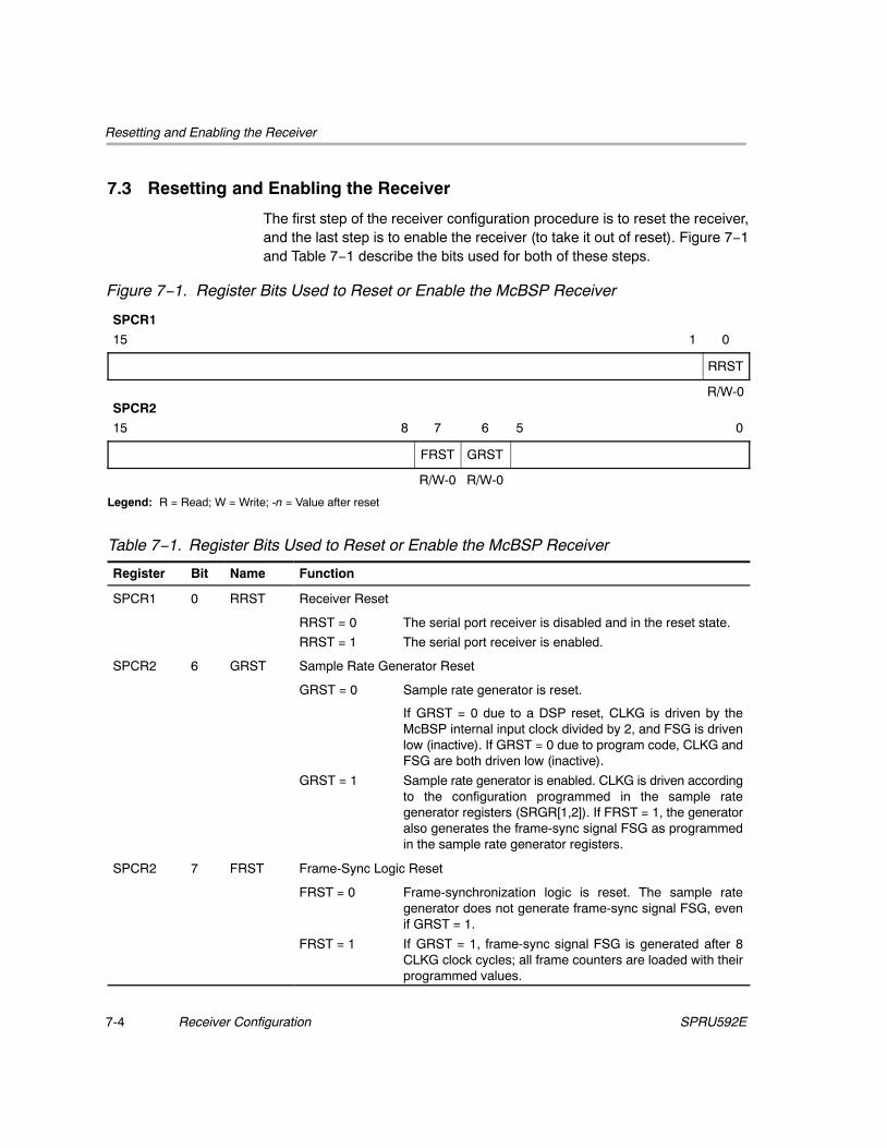
Resetting and Enabling the Receiver
Receiver Configuration7-4 SPRU592E
7.3 Resetting and Enabling the Receiver
The first step of the receiver configuration procedure is to reset the receiver,and the last step is to enable the receiver (to take it out of reset). Figure 7−1and Table 7−1 describe the bits used for both of these steps.
Figure 7−1. Register Bits Used to Reset or Enable the McBSP Receiver
SPCR1
15 1 0
RRST
R/W-0SPCR2
15 8 7 6 5 0
FRST GRST
R/W-0 R/W-0
Legend: R = Read; W = Write; -n = Value after reset
Table 7−1. Register Bits Used to Reset or Enable the McBSP Receiver
Register Bit Name Function
SPCR1 0 RRST Receiver Reset
RRST = 0 The serial port receiver is disabled and in the reset state.
RRST = 1 The serial port receiver is enabled.
SPCR2 6 GRST Sample Rate Generator Reset
GRST = 0 Sample rate generator is reset.
If GRST = 0 due to a DSP reset, CLKG is driven by theMcBSP internal input clock divided by 2, and FSG is drivenlow (inactive). If GRST = 0 due to program code, CLKG andFSG are both driven low (inactive).
GRST = 1 Sample rate generator is enabled. CLKG is driven accordingto the configuration programmed in the sample rategenerator registers (SRGR[1,2]). If FRST = 1, the generatoralso generates the frame-sync signal FSG as programmedin the sample rate generator registers.
SPCR2 7 FRST Frame-Sync Logic Reset
FRST = 0 Frame-synchronization logic is reset. The sample rategenerator does not generate frame-sync signal FSG, evenif GRST = 1.
FRST = 1 If GRST = 1, frame-sync signal FSG is generated after 8CLKG clock cycles; all frame counters are loaded with theirprogrammed values.

Resetting and Enabling the Receiver
7-5Receiver ConfigurationSPRU592E
7.3.1 Reset Considerations
The serial port can be reset in the following two ways:
1) A DSP reset (RESET signal driven low) places the receiver, transmitter,and sample rate generator in reset. When the device reset is removed(RESET signal driven high), GRST = FRST = RRST = XRST = 0,keeping the entire serial port in the reset state.
2) The serial port transmitter and receiver can be reset directly using theRRST and XRST bits in the serial port control registers. The sample rategenerator can be reset directly using the GRST bit in SPCR2.
Table 7−2 shows the state of McBSP pins when the serial port is reset due toa DSP reset and a direct receiver/transmitter reset.
Table 7−2. Reset State of Each McBSP Pin
PinPossibleState(s)
State Forced ByDSP Reset
State Forced ByReceiver/Transmitter Reset
Receiver Reset (RRST = 0 and GRST = 1)
DR I Input Input
CLKR I/O/Z Input Known state if Input; CLKR running if output
FSR I/O/Z Input Known state if Input; FSRP inactive state if output
CLKS I/O/Z Input Input
Transmitter Reset (XRST = 0 and GRST = 1)
DX O/Z High impedance High impedance
CLKX I/O/Z Input Known state if Input; CLKX running if output
FSX I/O/Z Input Known state if Input; FSXP inactive state if output
CLKS I Input Input
Note: In Possible State(s) column, I = Input, O = Output, Z = High impedance

Setting the Receiver Pins to Operate as McBSP Pins
Receiver Configuration7-6 SPRU592E
7.4 Setting the Receiver Pins to Operate as McBSP Pins
The RIOEN bit, shown in Figure 7−2 and described in Table 7−3, determineswhether the receiver pins are McBSP pins or general-purpose I/O pins.
Figure 7−2. Register Bit Used to Set Receiver Pins to Operate as McBSP Pins
PCR
15 13 12 11 0
RIOEN
R/W-0
Legend: R = Read; W = Write; -n = Value after reset
Table 7−3. Register Bit Used to Set Receiver Pins to Operate as McBSP Pins
Register Bit Name Function
PCR 12 RIOEN Receive I/O enable
This bit is only applicable when the receiver is in the reset state (RRST = 0 inSPCR1).
RIOEN = 0 The DR, FSR, CLKR, and CLKS pins are configured as serialport pins and do not function as general-purpose I/O pins.
RIOEN = 1 The DR pin is a general-purpose input pin. The FSR andCLKR pins are general purpose I/O pins. These serial portpins do not perform serial port operation. The CLKS pin is ageneral-purpose input pin if RIOEN = XIOEN = 1 andRRST = XRST = 0.

Enabling/Disabling the Digital Loopback Mode
7-7Receiver ConfigurationSPRU592E
7.5 Enabling/Disabling the Digital Loopback Mode
The DLB bit determines whether the digital loopback mode is on. DLB is shownin Figure 7−3 and described in Table 7−4.
Figure 7−3. Register Bit Used to Enable/Disable the Digital Loopback Mode
SPCR1
15 14 0
DLB
R/W-0
Legend: R = Read; W = Write; -n = Value after reset
Table 7−4. Register Bit Used to Enable/Disable the Digital Loopback Mode
Register Bit Name Function
SPCR1 15 DLB Digital Loopback Mode
DLB = 0 Digital loopback mode is disabled.
DLB = 1 Digital loopback mode is enabled.
7.5.1 About the Digital Loopback Mode
In the digital loopback mode, the receive signals are connected internallythrough multiplexers to the corresponding transmit signals, as shown inTable 7−5. This mode allows testing of serial port code with a single DSPdevice; the McBSP receives the data it transmits.
Table 7−5. Receive Signals Connected to Transmit Signals in Digital Loopback Mode
This Receive Signal …Is Fed Internally ByThis Transmit Signal …
DR (receive data) DX (transmit data)
FSR (receive frame synchronization) FSX (transmit frame synchronization)
CLKR (receive clock) CLKX (transmit clock)
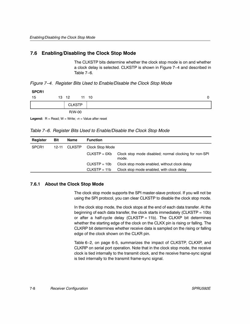
Enabling/Disabling the Clock Stop Mode
Receiver Configuration7-8 SPRU592E
7.6 Enabling/Disabling the Clock Stop Mode
The CLKSTP bits determine whether the clock stop mode is on and whethera clock delay is selected. CLKSTP is shown in Figure 7−4 and described inTable 7−6.
Figure 7−4. Register Bits Used to Enable/Disable the Clock Stop Mode
SPCR1
15 13 12 11 10 0
CLKSTP
R/W-00
Legend: R = Read; W = Write; -n = Value after reset
Table 7−6. Register Bits Used to Enable/Disable the Clock Stop Mode
Register Bit Name Function
SPCR1 12-11 CLKSTP Clock Stop Mode
CLKSTP = 0Xb Clock stop mode disabled; normal clocking for non-SPImode.
CLKSTP = 10b Clock stop mode enabled, without clock delay
CLKSTP = 11b Clock stop mode enabled, with clock delay
7.6.1 About the Clock Stop Mode
The clock stop mode supports the SPI master-slave protocol. If you will not beusing the SPI protocol, you can clear CLKSTP to disable the clock stop mode.
In the clock stop mode, the clock stops at the end of each data transfer. At thebeginning of each data transfer, the clock starts immediately (CLKSTP = 10b)or after a half-cycle delay (CLKSTP = 11b). The CLKXP bit determineswhether the starting edge of the clock on the CLKX pin is rising or falling. TheCLKRP bit determines whether receive data is sampled on the rising or fallingedge of the clock shown on the CLKR pin.
Table 6−2, on page 6-5, summarizes the impact of CLKSTP, CLKXP, andCLKRP on serial port operation. Note that in the clock stop mode, the receiveclock is tied internally to the transmit clock, and the receive frame-sync signalis tied internally to the transmit frame-sync signal.

Enabling/Disabling the Receive Multichannel Selection Mode
7-9Receiver ConfigurationSPRU592E
7.7 Enabling/Disabling the Receive Multichannel Selection Mode
The RMCM bit determines whether the receive multichannel selection modeis on. RMCM is shown in Figure 7−5 and described in Table 7−7.
Figure 7−5. Register Bit Used to Enable/Disable the Receive Multichannel Selection Mode
MCR1
15 1 0
RMCM
R/W-0
Legend: R = Read; W = Write; -n = Value after reset
Table 7−7. Register Bit Used to Enable/Disable theReceive Multichannel Selection Mode
Register Bit Name Function
MCR1 0 RMCM Receive Multichannel Selection Mode
RMCM = 0 The mode is disabled.
All 128 channels are enabled.
RMCM = 1 The mode is enabled.
Channels can be individually enabled or disabled.
The only channels enabled are those selected in theappropriate receive channel enable registers (RCERs).The way channels are assigned to the RCERs depends onthe number of receive channel partitions (2 or 8), as definedby the RMCME bit.

Choosing One or Two Phases for the Receive Frame
Receiver Configuration7-10 SPRU592E
7.8 Choosing One or Two Phases for the Receive Frame
The RPHASE bit (see Figure 7−6 and Table 7−8) determines whether thereceive data frame has one or two phases.
Figure 7−6. Register Bit Used to Choose One or Two Phases for the Receive Frame
RCR2
15 14 0
RPHASE
R/W-0
Legend: R = Read; W = Write; -n = Value after reset
Table 7−8. Register Bit Used to Choose One or Two Phases for the Receive Frame
Register Bit Name Function
RCR2 15 RPHASE Receive phase number
Specifies whether the receive frame has one or two phases.
RPHASE = 0 Single-phase frame
RPHASE = 1 Dual-phase frame

Setting the Receive Word Length(s)
7-11Receiver ConfigurationSPRU592E
7.9 Setting the Receive Word Length(s)
The RWDLEN1 and RWDLEN2 fields (see Figure 7−7 and Table 7−9)determine how many bits are in each serial word in phase 1 and in phase 2,respectively, of the receive data frame.
Figure 7−7. Register Bits Used to Set the Receive Word Length(s)
RCR1
15 8 7 5 4 0
RWDLEN1
R/W-000RCR2
15 8 7 5 4 0
RWDLEN2
R/W-000
Legend: R = Read; W = Write; -n = Value after reset
Table 7−9. Register Bits Used to Set the Receive Word Length(s)
Register Bit Name Function
RCR1 7-5 RWDLEN1 Receive word length 1
Specifies the length of every serial word in phase 1 of the receive frame.
RWDLEN1 = 000 8 bits
RWDLEN1 = 001 12 bits
RWDLEN1 = 010 16 bits
RWDLEN1 = 011 20 bits
RWDLEN1 = 100 24 bits
RWDLEN1 = 101 32 bits
RWDLEN1 = 11X Reserved
RCR2 7-5 RWDLEN2 Receive word length 2
If a dual-phase frame is selected, RWDLEN2 specifies the length of everyserial word in phase 2 of the frame.
RWDLEN2 = 000 8 bits
RWDLEN2 = 001 12 bits
RWDLEN2 = 010 16 bits
RWDLEN2 = 011 20 bits
RWDLEN2 = 100 24 bits
RWDLEN2 = 101 32 bits
RWDLEN2 = 11X Reserved
Setting the Receive Word Length(s)
Receiver Configuration7-12 SPRU592E
7.9.1 About the Word Length Bits
Each frame can have one or two phases, depending on the value that you loadinto the RPHASE bit. If a single-phase frame is selected, RWDLEN1 selectsthe length for every serial word received in the frame and RWDLEN2 isignored. If a dual-phase frame is selected, RWDLEN1 determines the lengthof the serial words in phase 1 of the frame, and RWDLEN2 determines theword length in phase 2 of the frame.

Setting the Receive Frame Length
7-13Receiver ConfigurationSPRU592E
7.10 Setting the Receive Frame Length
The RFRLEN1 and RFRLEN2 bit fields (see Figure 7−8 and Table 7−10)determine how many serial words are in phase 1 and in phase 2, respectively,of the receive data frame.
Figure 7−8. Register Bits Used to Set the Receive Frame Length
RCR1
15 14 8 7 0
RFRLEN1
R/W-000 0000RCR2
15 14 8 7 0
RFRLEN2
R/W-000 0000
Legend: R = Read; W = Write; -n = Value after reset
Table 7−10. Register Bits Used to Set the Receive Frame Length
Register Bit Name Function
RCR1 14-8 RFRLEN1 Receive frame length 1
(RFRLEN1 + 1) is the number of serial words in phase 1 of the receive frame.
RFRLEN1 = 000 0000 1 word in phase 1
RFRLEN1 = 000 0001 2 words in phase 1
| |
| |
RFRLEN1 = 111 1111 128 words in phase 1
RCR2 14-8 RFRLEN2 Receive frame length 2
If a dual-phase frame is selected, (RFRLEN2 + 1) is the number of serial wordsin phase 2 of the receive frame. If a single-phase frame is selected, RFRLEN2is ignored.
RFRLEN2 = 000 0000 1 word in phase 2
RFRLEN2 = 000 0001 2 words in phase 2
| |
| |
RFRLEN2 = 111 1111 128 words in phase 2

Setting the Receive Frame Length
Receiver Configuration7-14 SPRU592E
7.10.1 About the Selected Frame Length
The receive frame length is the number of serial words in the receive frame.Each frame can have one or two phases, depending on the value that you loadinto the RPHASE bit.
If a single-phase frame is selected (RPHASE = 0), the frame length is equalto the length of phase 1. If a dual-phase frame is selected (RPHASE = 1), theframe length is the length of phase 1 plus the length of phase 2:
The 7-bit RFRLEN fields allow up to 128 words per phase. See Table 7−11 fora summary of how to calculate the frame length. This length corresponds tothe number of words or logical time slots or channels perframe-synchronization pulse.
Note: Program the RFRLEN fields with [w minus 1], where w represents thenumber of words per phase. For example, if you want a phase length of 128words in phase 1, load 127 into RFRLEN1.
Table 7−11. How to Calculate the Length of the Receive Frame
RPHASE RFRLEN1 RFRLEN2 Frame Length
0 0 ≤ RFRLEN1 ≤ 127 Don’t care (RFRLEN1 + 1) words
1 0 ≤ RFRLEN1 ≤ 127 0 ≤ RFRLEN2 ≤ 127 (RFRLEN1 + 1) + (RFRLEN2 + 1) words
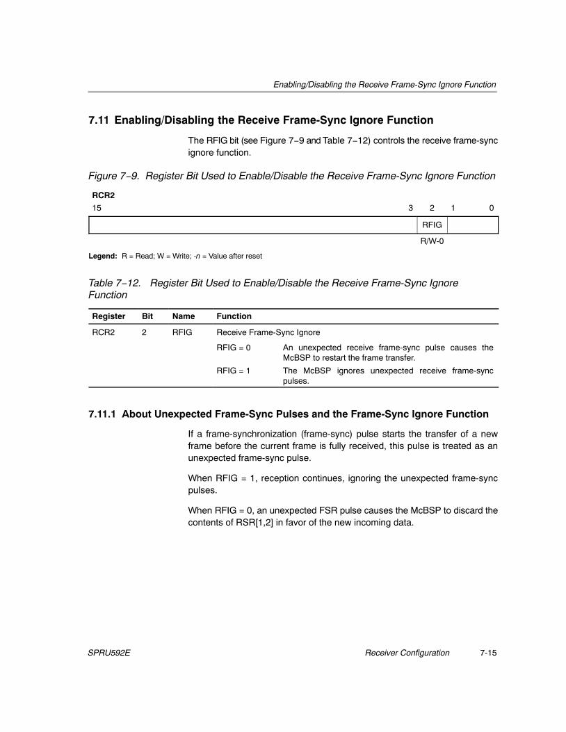
Enabling/Disabling the Receive Frame-Sync Ignore Function
7-15Receiver ConfigurationSPRU592E
7.11 Enabling/Disabling the Receive Frame-Sync Ignore Function
The RFIG bit (see Figure 7−9 and Table 7−12) controls the receive frame-syncignore function.
Figure 7−9. Register Bit Used to Enable/Disable the Receive Frame-Sync Ignore Function
RCR2
15 3 2 1 0
RFIG
R/W-0
Legend: R = Read; W = Write; -n = Value after reset
Table 7−12. Register Bit Used to Enable/Disable the Receive Frame-Sync IgnoreFunction
Register Bit Name Function
RCR2 2 RFIG Receive Frame-Sync Ignore
RFIG = 0 An unexpected receive frame-sync pulse causes theMcBSP to restart the frame transfer.
RFIG = 1 The McBSP ignores unexpected receive frame-syncpulses.
7.11.1 About Unexpected Frame-Sync Pulses and the Frame-Sync Ignore Function
If a frame-synchronization (frame-sync) pulse starts the transfer of a newframe before the current frame is fully received, this pulse is treated as anunexpected frame-sync pulse.
When RFIG = 1, reception continues, ignoring the unexpected frame-syncpulses.
When RFIG = 0, an unexpected FSR pulse causes the McBSP to discard thecontents of RSR[1,2] in favor of the new incoming data.
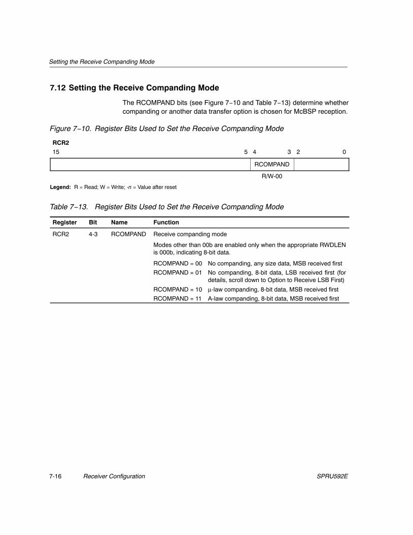
Setting the Receive Companding Mode
Receiver Configuration7-16 SPRU592E
7.12 Setting the Receive Companding Mode
The RCOMPAND bits (see Figure 7−10 and Table 7−13) determine whethercompanding or another data transfer option is chosen for McBSP reception.
Figure 7−10. Register Bits Used to Set the Receive Companding Mode
RCR2
15 5 4 3 2 0
RCOMPAND
R/W-00
Legend: R = Read; W = Write; -n = Value after reset
Table 7−13. Register Bits Used to Set the Receive Companding Mode
Register Bit Name Function
RCR2 4-3 RCOMPAND Receive companding mode
Modes other than 00b are enabled only when the appropriate RWDLENis 000b, indicating 8-bit data.
RCOMPAND = 00 No companding, any size data, MSB received first
RCOMPAND = 01 No companding, 8-bit data, LSB received first (fordetails, scroll down to Option to Receive LSB First)
RCOMPAND = 10 µ-law companding, 8-bit data, MSB received first
RCOMPAND = 11 A-law companding, 8-bit data, MSB received first

Setting the Receive Data Delay
7-17Receiver ConfigurationSPRU592E
7.13 Setting the Receive Data Delay
The RDATDLY bits (see Figure 7−11 and Table 7−14) determine the length ofthe data delay for the receive frame.
Figure 7−11.Register Bits Used to Set the Receive Data Delay
RCR2
15 2 1 0
RDATDLY
R/W-00
Legend: R = Read; W = Write; -n = Value after reset
Table 7−14. Register Bits Used to Set the Receive Data Delay
Register Bit Name Function
RCR2 1-0 RDATDLY Receive data delay
RDATDLY = 00 0-bit data delay
RDATDLY = 01 1-bit data delay
RDATDLY = 10 2-bit data delay
RDATDLY = 11 Reserved
7.13.1 About the Data Delay
The start of a frame is defined by the first clock cycle in which framesynchronization is found to be active. The beginning of actual data receptionor transmission, with respect to the start of the frame, can be delayed ifrequired. This delay is called data delay.
RDATDLY specifies the data delay for reception. The range of programmabledata delay is zero to two bit-clocks (RDATDLY = 00b–10b), as described inTable 7−14 and shown in Figure 7−12. In this figure, the data transferred is an8-bit value with bits labeled B7, B6, B5, and so on. Typically a 1-bit delay isselected, because data often follows a 1-cycle active frame-sync pulse.

Setting the Receive Data Delay
Receiver Configuration7-18 SPRU592E
Figure 7−12. Range of Programmable Data Delay
B5B6B7
B4B5B6B7
B3B4B5B6B7
Data delay 2D(R/X)
Data delay 1D(R/X)
Data delay 0D(R/X)
FS(R/X)
CLK(R/X)
1-bit delay
ÁÁ
ÁÁ
ÁÁÁÁ
0-bit delay
2-bit delay
7.13.2 0-Bit Data Delay
Normally, a frame-sync pulse is detected or sampled with respect to an edgeof internal serial clock CLK(R/X). Therefore, on the following cycle or later(depending on the data delay value), data may be received or transmitted.However, in the case of 0-bit data delay, the data must be ready for receptionand/or transmission on the same serial clock cycle.
This problem is solved for reception because receive data is sampled on thefirst falling edge of CLKR where an active-high internal FSR is detected.However, data transmission must begin on the rising edge of the internal CLKXclock that generated the frame synchronization. Therefore, the first data bit isassumed to be present in XSR1, and thus on DX. The transmitter thenasynchronously detects the frame-sync signal (FSX) going active high andimmediately starts driving the first bit to be transmitted on the DX pin.
7.13.3 2-Bit Data Delay
A data delay of two bit periods allows the serial port to interface to differenttypes of T1 framing devices where the data stream is preceded by a framingbit. During reception of such a stream with a data delay of two bits (framing bitappears after a 1-bit delay and data appears after a 2-bit delay), the serial portessentially discards the framing bit from the data stream, as shown inFigure 7−13. In this figure, the data transferred is an 8-bit value with bitslabeled B7, B6, B5, and so on.

Setting the Receive Data Delay
7-19Receiver ConfigurationSPRU592E
Figure 7−13. 2-Bit Data Delay Used to Skip a Framing Bit
DR Framing bit B5B6B7
FSR
CLKR
ÁÁ
2-bit delay

Setting the Receive Sign-Extension and Justification Mode
Receiver Configuration7-20 SPRU592E
7.14 Setting the Receive Sign-Extension and Justification Mode
The RJUST bits (see Figure 7−14 and Table 7−15) determine whether datareceived by the McBSP is sign extended and how it is justified.
Figure 7−14. Register Bits Used to Set the Receive Sign-Extension and Justification Mode
SPCR1
15 14 13 12 0
RJUST
R/W-00
Legend: R = Read; W = Write; -n = Value after reset
Table 7−15. Register Bits Used to Set the Receive Sign-Extension and Justification Mode
Register Bit Name Function
SPCR1 14-13 RJUST Receive Sign-Extension and Justification Mode
RJUST = 00 Right justify data and zero fill MSBs in DRR[1,2]
RJUST = 01 Right justify data and sign extend it into the MSBs inDRR[1,2]
RJUST = 10 Left justify data and zero fill LSBs in DRR[1,2]
RJUST = 11 Reserved
7.14.1 About the Sign Extension and the Justification
RJUST in SPCR1 selects whether data in RBR[1,2] is right- or left-justified(with respect to the MSB) in DRR[1,2] and how unused bits in DRR[1,2] arefilled—with zeros or with sign bits.
Table 7−16 and Table 7−17 show the effects of various RJUST values. Thefirst table shows the effect on an example 12-bit receive-data value 0xABC.The second table shows the effect on an example 20-bit receive-data value0xABCDE.
Table 7−16. Example: Use of RJUST Field With 12-Bit Data Value 0xABC
RJUST Justification ExtensionValue inDRR2
Value inDRR1
00b Right Zero fill MSBs 0000h 0ABCh
01b Right Sign extend data intoMSBs
FFFFh FABCh
10b Left Zero fill LSBs 0000h ABC0h
11b Reserved Reserved Reserved Reserved

Setting the Receive Sign-Extension and Justification Mode
7-21Receiver ConfigurationSPRU592E
Table 7−17. Example: Use of RJUST Field With 20-Bit Data Value 0xABCDE
RJUST Justification ExtensionValue inDRR2
Value inDRR1
00b Right Zero fill MSBs 000Ah BCDEh
01b Right Sign extend data intoMSBs
FFFAh BCDEh
10b Left Zero fill LSBs ABCDh E000h
11b Reserved Reserved Reserved Reserved
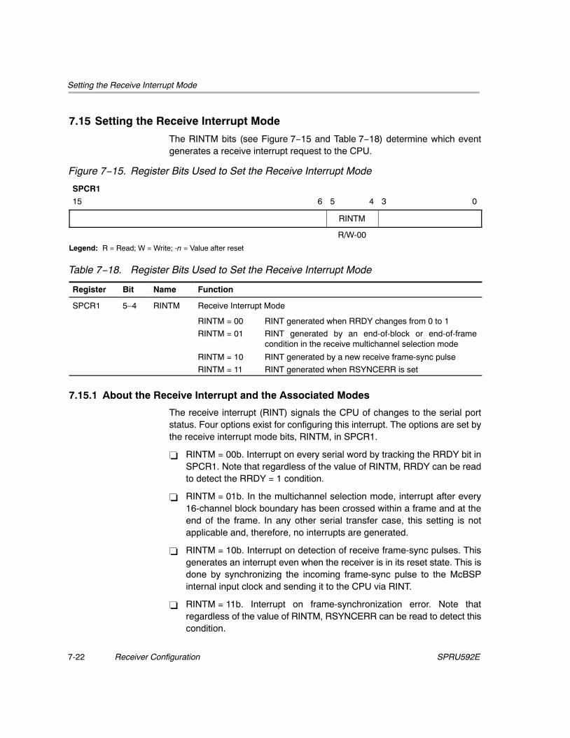
Setting the Receive Interrupt Mode
Receiver Configuration7-22 SPRU592E
7.15 Setting the Receive Interrupt Mode
The RINTM bits (see Figure 7−15 and Table 7−18) determine which eventgenerates a receive interrupt request to the CPU.
Figure 7−15. Register Bits Used to Set the Receive Interrupt Mode
SPCR1
15 6 5 4 3 0
RINTM
R/W-00
Legend: R = Read; W = Write; -n = Value after reset
Table 7−18. Register Bits Used to Set the Receive Interrupt Mode
Register Bit Name Function
SPCR1 5–4 RINTM Receive Interrupt Mode
RINTM = 00 RINT generated when RRDY changes from 0 to 1
RINTM = 01 RINT generated by an end-of-block or end-of-framecondition in the receive multichannel selection mode
RINTM = 10 RINT generated by a new receive frame-sync pulse
RINTM = 11 RINT generated when RSYNCERR is set
7.15.1 About the Receive Interrupt and the Associated Modes
The receive interrupt (RINT) signals the CPU of changes to the serial portstatus. Four options exist for configuring this interrupt. The options are set bythe receive interrupt mode bits, RINTM, in SPCR1.
� RINTM = 00b. Interrupt on every serial word by tracking the RRDY bit inSPCR1. Note that regardless of the value of RINTM, RRDY can be readto detect the RRDY = 1 condition.
� RINTM = 01b. In the multichannel selection mode, interrupt after every16-channel block boundary has been crossed within a frame and at theend of the frame. In any other serial transfer case, this setting is notapplicable and, therefore, no interrupts are generated.
� RINTM = 10b. Interrupt on detection of receive frame-sync pulses. Thisgenerates an interrupt even when the receiver is in its reset state. This isdone by synchronizing the incoming frame-sync pulse to the McBSPinternal input clock and sending it to the CPU via RINT.
� RINTM = 11b. Interrupt on frame-synchronization error. Note thatregardless of the value of RINTM, RSYNCERR can be read to detect thiscondition.

Setting the Receive Frame-Sync Mode
7-23Receiver ConfigurationSPRU592E
7.16 Setting the Receive Frame-Sync Mode
The bits shown in Figure 7−16 and described in Table 7−19 determine thesource for receive frame synchronization and the function of the FSR pin.
Figure 7−16. Register Bits Used to Set the Receive Frame Sync Mode
PCR
15 11 10 9 0
FSRM
R/W-0SRGR2
15 14 0
GSYNC
R/W-0SPCR1
15 14 13 12 11 10 0
DLB CLKSTP
R/W-0 R/W-00
Legend: R = Read; W = Write; -n = Value after reset
Table 7−19. Register Bits Used to Set the Receive Frame Sync Mode
Register Bit Name Function
PCR 10 FSRM Receive Frame-Synchronization Mode
FSRM = 0 Receive frame synchronization is supplied by an externalsource via the FSR pin.
FSRM = 1 Receive frame synchronization is supplied by the samplerate generator. FSR is an output pin reflecting internalFSR, except when GSYNC = 1 in SRGR2.
† The clock synchronization provided through the GSYNC bit is not supported on TMS320VC5501 and TMS320VC5502devices.
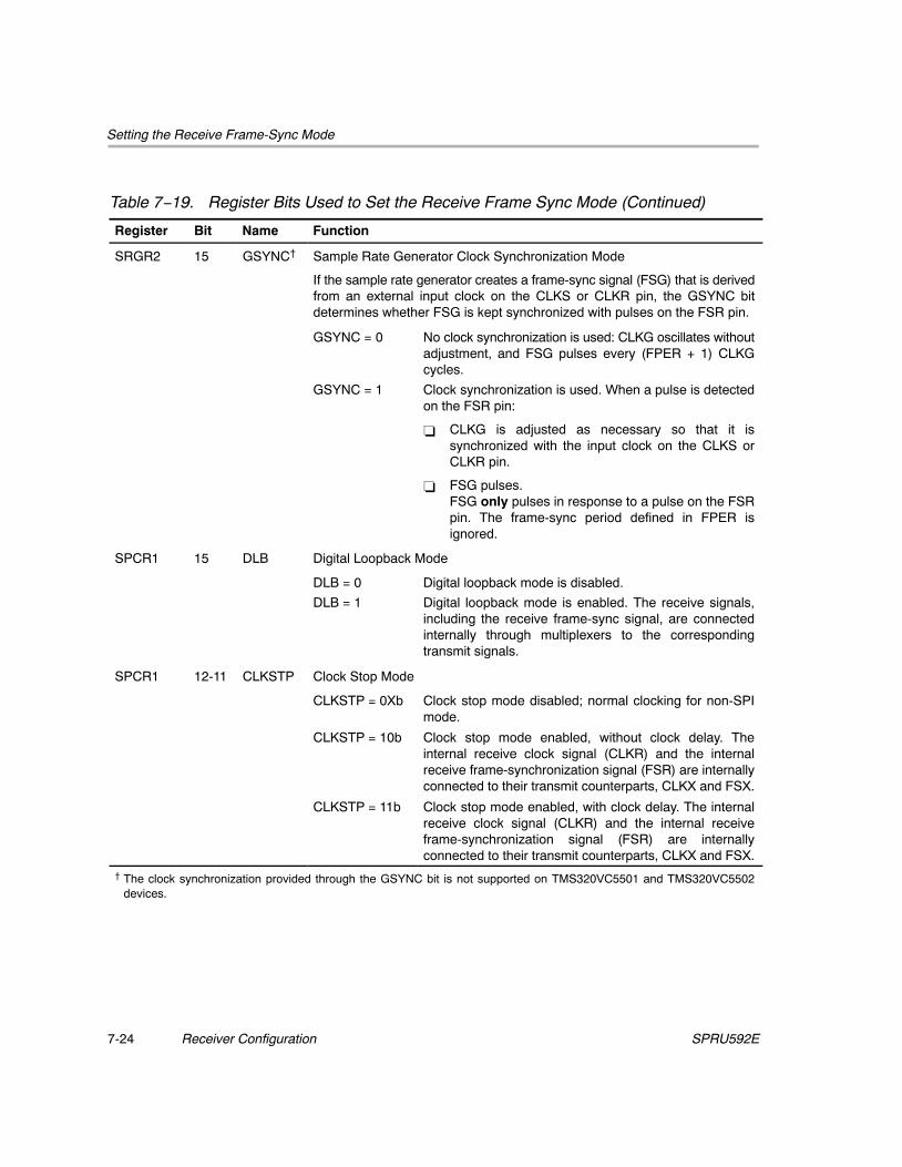
Setting the Receive Frame-Sync Mode
Receiver Configuration7-24 SPRU592E
Table 7−19. Register Bits Used to Set the Receive Frame Sync Mode (Continued)
Register FunctionNameBit
SRGR2 15 GSYNC† Sample Rate Generator Clock Synchronization Mode
If the sample rate generator creates a frame-sync signal (FSG) that is derivedfrom an external input clock on the CLKS or CLKR pin, the GSYNC bitdetermines whether FSG is kept synchronized with pulses on the FSR pin.
GSYNC = 0 No clock synchronization is used: CLKG oscillates withoutadjustment, and FSG pulses every (FPER + 1) CLKGcycles.
GSYNC = 1 Clock synchronization is used. When a pulse is detectedon the FSR pin:
� CLKG is adjusted as necessary so that it issynchronized with the input clock on the CLKS orCLKR pin.
� FSG pulses.FSG only pulses in response to a pulse on the FSRpin. The frame-sync period defined in FPER isignored.
SPCR1 15 DLB Digital Loopback Mode
DLB = 0 Digital loopback mode is disabled.
DLB = 1 Digital loopback mode is enabled. The receive signals,including the receive frame-sync signal, are connectedinternally through multiplexers to the correspondingtransmit signals.
SPCR1 12-11 CLKSTP Clock Stop Mode
CLKSTP = 0Xb Clock stop mode disabled; normal clocking for non-SPImode.
CLKSTP = 10b Clock stop mode enabled, without clock delay. Theinternal receive clock signal (CLKR) and the internalreceive frame-synchronization signal (FSR) are internallyconnected to their transmit counterparts, CLKX and FSX.
CLKSTP = 11b Clock stop mode enabled, with clock delay. The internalreceive clock signal (CLKR) and the internal receiveframe-synchronization signal (FSR) are internallyconnected to their transmit counterparts, CLKX and FSX.
† The clock synchronization provided through the GSYNC bit is not supported on TMS320VC5501 and TMS320VC5502devices.

Setting the Receive Frame-Sync Mode
7-25Receiver ConfigurationSPRU592E
7.16.1 About the Receive Frame-Sync Modes
Table 7−20 shows how you may select various sources to provide the receiveframe-synchronization signal and the effect on the FSR pin. The polarity of thesignal on the FSR pin is determined by the FSRP bit.
Note that in the digital loop back mode (DLB = 1), the transmit frame-syncsignal is used as the receive frame-sync signal.
Also, in the clock stop mode, the internal receive clock signal (CLKR) and theinternal receive frame-synchronization signal (FSR) are internally connectedto their transmit counterparts, CLKX and FSX.
Table 7−20. Select Sources to Provide the Receive Frame-Synchronization Signal andthe Effect on the FSR Pin
DLB FSRM GSYNC†Source of Receive FrameSynchronization FSR Pin Status
0 0 0 or 1 An external frame-sync signalenters the McBSP through the FSRpin. The signal is then inverted asdetermined by FSRP before beingused as internal FSR.
Input
0 1 0 Internal FSR is driven by thesample rate generator frame-syncsignal (FSG).
Output. FSG is inverted asdetermined by FSRP before beingdriven out on the FSR pin.
0 1 1 Internal FSR is driven by thesample rate generator frame-syncsignal (FSG).
Input. The external frame-syncinput on the FSR pin is used tosynchronize CLKG and generateFSG pulses.
1 0 0 Internal FSX drives internal FSR. High impedance
1 0 or 1 1 Internal FSX drives internal FSR. Input. If the sample rate generatoris running, external FSR is used tosynchronize CLKG and generateFSG pulses.
1 1 0 Internal FSX drives internal FSR. Output. Receive (same astransmit) frame synchronization isinverted as determined by FSRPbefore being driven out on the FSRpin.
† The clock synchronization provided through the GSYNC bit is not supported on TMS320VC5501 and TMS320VC5502devices.

Setting the Receive Frame-Sync Polarity
Receiver Configuration7-26 SPRU592E
7.17 Setting the Receive Frame-Sync Polarity
The FSRP bit (see Figure 7−17 and Table 7−21) determines whetherframe-synchronization (frame-sync) pulses are active high or active low on theFSR pin.
Figure 7−17. Register Bit Used to Set Receive Frame-Sync Polarity
PCR
15 3 2 1 0
FSRP
R/W-0
Legend: R = Read; W = Write; -n = Value after reset
Table 7−21. Register Bit Used to Set Receive Frame-Sync Polarity
Register Bit Name Function
PCR 2 FSRP Receive Frame-Synchronization Polarity
FSRP = 0 Frame-synchronization pulse FSR is active high.
FSRP = 1 Frame-synchronization pulse FSR is active low.
7.17.1 About Frame Sync Pulses, Clock Signals, and Their Polarities
Receive frame-sync pulses can be either generated internally by the samplerate generator or driven by an external source. The source of frame sync isselected by programming the mode bit, FSRM, in PCR. FSR is also affectedby the GSYNC bit in SRGR2. Similarly, receive clocks can be selected to beinputs or outputs by programming the mode bit, CLKRM, in the PCR.
When FSR and FSX are inputs (FSXM = FSRM= 0, external frame-syncpulses), the McBSP detects them on the internal falling edge of clock, internalCLKR, and internal CLKX, respectively. The receive data arriving at the DR pinis also sampled on the falling edge of internal CLKR. Note that these internalclock signals are either derived from external source via CLK(R/X) pins ordriven by the sample rate generator clock (CLKG) internal to the McBSP.
When FSR and FSX are outputs, implying that they are driven by the samplerate generator, they are generated (transition to their active state) on the risingedge of internal clock, CLK(R/X). Similarly, data on the DX pin is output on therising edge of internal CLKX.

Setting the Receive Frame-Sync Polarity
7-27Receiver ConfigurationSPRU592E
FSRP, FSXP, CLKRP, and CLKXP in the pin control register (PCR) configurethe polarities of the FSR, FSX, CLKR, and CLKX signals, respectively. Allframe-sync signals (internal FSR, internal FSX) that are internal to the serialport are active high. If the serial port is configured for external framesynchronization (FSR/FSX are inputs to McBSP), and FSRP = FSXP = 1, theexternal active-low frame-sync signals are inverted before being sent to thereceiver (internal FSR) and transmitter (internal FSX). Similarly, if internalsynchronization (FSR/FSX are output pins and GSYNC = 0) is selected, theinternal active-high frame-sync signals are inverted, if the polarity bitFS(R/X)P = 1, before being sent to the FS(R/X) pin.
On the transmit side, the transmit clock polarity bit, CLKXP, sets the edge usedto shift and clock out transmit data. Note that data is always transmitted on therising edge of internal CLKX. If CLKXP = 1, and external clocking is selected(CLKXM = 0 and CLKX is an input), the external falling-edge triggered inputclock on CLKX is inverted to a rising-edge triggered clock before being sentto the transmitter. If CLKXP = 1, and internal clocking selected (CLKXM = 1and CLKX is an output pin), the internal (rising-edge triggered) clock, internalCLKX, is inverted before being sent out on the CLKX pin.
Similarly, the receiver can reliably sample data that is clocked with a risingedge clock (by the transmitter). The receive clock polarity bit, CLKRP, sets theedge used to sample received data. Note that the receive data is alwayssampled on the falling edge of internal CLKR. Therefore, if CLKRP = 1 andexternal clocking is selected (CLKRM = 0 and CLKR is an input pin), theexternal rising-edge triggered input clock on CLKR is inverted to a falling-edgetriggered clock before being sent to the receiver. If CLKRP = 1, and internalclocking is selected (CLKRM = 1), the internal falling-edge triggered clock isinverted to a rising-edge triggered clock before being sent out on the CLKR pin.
Note that CLKRP = CLKXP in a system where the same clock (internal orexternal) is used to clock the receiver and transmitter. The receiver uses theopposite edge as the transmitter to ensure valid setup and hold of data aroundthis edge. Figure 7−18 shows how data clocked by an external serial deviceusing a rising edge can be sampled by the McBSP receiver on the falling edgeof the same clock.
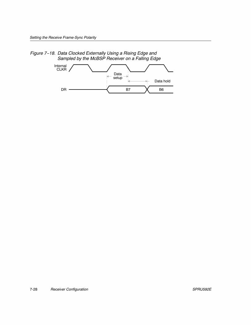
Setting the Receive Frame-Sync Polarity
Receiver Configuration7-28 SPRU592E
Figure 7−18. Data Clocked Externally Using a Rising Edge andSampled by the McBSP Receiver on a Falling Edge
Datasetup
Data hold
B7 B6
InternalCLKR
DR

Setting the SRG Frame-Sync Period and Pulse Width
7-29Receiver ConfigurationSPRU592E
7.18 Setting the SRG Frame-Sync Period and Pulse Width
The FPER and FWID fields, shown in Figure 7−19 and described inTable 7−22, are used to set the SRG frame-sync period and pulse width.
Figure 7−19. Register Bits Used to Set the SRG Frame-Sync Period and Pulse Width
SRGR2
15 12 11 0
FPER
R/W-0000 0000 0000SRGR1
15 8 7 0
FWID
R/W-0000 0000
Legend: R = Read; W = Write; -n = Value after reset
Table 7−22. Register Bits Used to Set the SRG Frame-Sync Period and Pulse Width
Register Bit Name Function
SRGR2 11-0 FPER Sample Rate Generator Frame-Sync Period
For the frame-sync signal FSG, (FPER + 1) determines the period from thestart of a frame-sync pulse to the start of the next frame-sync pulse.
Range for (FPER + 1): 1 to 4096 CLKG cycles.
SRGR1 15-8 FWID Sample Rate Generator Frame-Sync Pulse Width
This field plus 1 determines the width of each frame-sync pulse on FSG.
Range for (FWID + 1): 1 to 256 CLKG cycles.

Setting the SRG Frame-Sync Period and Pulse Width
Receiver Configuration7-30 SPRU592E
7.18.1 About the Frame-Sync Period and the Frame-Sync Pulse Width
The sample rate generator can produce a clock signal, CLKG, and aframe-sync signal, FSG. If the sample rate generator is supplying receive ortransmit frame synchronization, you must program the bit fields FPER andFWID.
On FSG, the period from the start of a frame-sync pulse to the start of the nextpulse is (FPER + 1) CLKG cycles. The 12 bits of FPER allow a frame-syncperiod of 1 to 4096 CLKG cycles, which allows up to 4096 data bits per frame.When GSYNC = 1, FPER is a don’t care value.
Each pulse on FSG has a width of (FWID + 1) CLKG cycles. The eight bits ofFWID allow a pulse width of 1 to 256 CLKG cycles. It is recommended thatFWID be programmed to a value less than the programmed word length.
The values in FPER and FWID are loaded into separate down-counters. The12-bit FPER counter counts down the generated clock cycles from theprogrammed value (4095 maximum) to 0. The 8-bit FWID counter countsdown from the programmed value (255 maximum) to 0.
Figure 7−20 shows a frame-sync period of 16 CLKG periods(FPER = 15 or 00001111b) and a frame-sync pulse with an active width of 2CLKG periods (FWID = 1).
Figure 7−20. Frame of Period 16 CLKG Periods and Active Width of 2 CLKG Periods
FSG
CLKG
19181716151413121110987654321
Frame-sync period: (FPER+1) x CLKG
Frame-sync pulse width: (FWID + 1) x CLKG
When the sample rate generator comes out of reset, FSG is in its inactive state.Then, when FRST = 1 and FSGM = 1, a frame-sync pulse is generated. Theframe width value (FWID + 1) is counted down on every CLKG cycle until itreaches 0, at which time FSG goes low. At the same time, the frame periodvalue (FPER + 1) is also counting down. When this value reaches 0, FSG goeshigh, indicating a new frame.

Setting the Receive Clock Mode
7-31Receiver ConfigurationSPRU592E
7.19 Setting the Receive Clock Mode
The bits shown in Figure 7−21 and described in Table 7−23 determine thesource for receive clock and the function of the CLKR pin.
Figure 7−21. Register Bits Used to Set the Receive Clock Mode
PCR
15 9 8 7 0
CLKRM
R/W-0SPCR1
15 14 13 12 11 10 0
DLB CLKSTP
R/W-0 R/W-00
Legend: R = Read; W = Write; -n = Value after reset
Table 7−23. Register Bits Used to Set the Receive Clock Mode
Register Bit Name Function
PCR 8 CLKRM Receive Clock Mode
Case 1: Digital loopback mode not set (DLB = 0) in SPCR1.
CLKRM = 0 The CLKR pin is an input pin that supplies the internalreceive clock (CLKR).
CLKRM = 1 Internal CLKR is driven by the sample rate generator of theMcBSP. The CLKR pin is an output pin that reflects internalCLKR.
Case 2: Digital loopback mode set (DLB = 1) in SPCR1.
CLKRM = 0 The CLKR pin is in the high-impedance state. The internalreceive clock (CLKR) is driven by the internal transmitclock (CLKX). Internal CLKX is derived according to theCLKXM bit of PCR.
CLKRM = 1 Internal CLKR is driven by internal CLKX. The CLKR pinis an output pin that reflects internal CLKR. Internal CLKXis derived according to the CLKXM bit of PCR.
SPCR1 15 DLB Digital Loopback Mode
DLB = 0 Digital loopback mode is disabled.
DLB = 1 Digital loopback mode is enabled. The receive signals,including the receive frame-sync signal, are connectedinternally through multiplexers to the correspondingtransmit signals.

Setting the Receive Clock Mode
Receiver Configuration7-32 SPRU592E
Table 7−23. Register Bits Used to Set the Receive Clock Mode (Continued)
Register FunctionNameBit
SPCR1 12-11 CLKSTP Clock Stop Mode
CLKSTP = 0Xb Clock stop mode disabled; normal clocking for non-SPImode.
CLKSTP = 10b Clock stop mode enabled, without clock delay. Theinternal receive clock signal (CLKR) and the internalreceive frame-synchronization signal (FSR) are internallyconnected to their transmit counterparts, CLKX and FSX.
CLKSTP = 11b Clock stop mode enabled, with clock delay. The internalreceive clock signal (CLKR) and the internal receiveframe-synchronization signal (FSR) are internallyconnected to their transmit counterparts, CLKX and FSX.
7.19.1 Selecting a Source for the Receive Clock and a Data Direction for theCLKR Pin
Table 7−24 shows how you can select various sources to provide the receiveclock signal and the effect on the CLKR pin. The polarity of the signal on theCLKR pin is determined by the CLKRP bit.
Note that in the digital loop back mode (DLB = 1), the transmit clock signal isalso used as the receive clock signal.
Also, in the clock stop mode, the internal receive clock signal (CLKR) and theinternal receive frame-synchronization signal (FSR) are internally connectedto their transmit counterparts, CLKX and FSX.

Setting the Receive Clock Mode
7-33Receiver ConfigurationSPRU592E
Table 7−24. Select Sources to Provide the Receive Clock Signal and the Effect on theCLKR Pin
DLB inSPCR1
CLKRM inPCR Source of Receive Clock CLKR Pin Status
0 0 The CLKR pin is an input driven by anexternal clock. The external clocksignal is inverted as determined byCLKRP before being used.
Input
0 1 The sample rate generator clock(CLKG) drives internal CLKR.
Output. CLKG, inverted as determined byCLKRP, is driven out on the CLKR pin.
1 0 Internal CLKX drives internal CLKR.For details on configuring CLKX, seeChapter 8, Transmitter Configuration.
High impedance
1 1 Internal CLKX drives internal CLKR.For details on configuring CLKX, seeChapter 8, Transmitter Configuration.
Output. Internal CLKR (same as internalCLKX) is inverted as determined by CLKRPbefore being driven out on the CLKR pin.

Setting the Receive Clock Polarity
Receiver Configuration7-34 SPRU592E
7.20 Setting the Receive Clock Polarity
The CLKRP bit (see Figure 7−22 and Table 7−25) determines the receiveclock polarity.
Figure 7−22. Register Bit Used to Set Receive Clock Polarity
PCR
15 1 0
CLKRP
R/W-0
Legend: R = Read; W = Write; -n = Value after reset
Table 7−25. Register Bit Used to Set Receive Clock Polarity
Register Bit Name Function
PCR 0 CLKRP Receive Clock Polarity
CLKRP = 0 When CLKR is configured as a input, the external CLKR isnot inverted before being used internally.
When CLKR is configured as an output, the internal CLKRis not inverted before being driven on the CLKR pin.
The receive data is sampled on the falling edge of theexternal CLKR signal.
CLKRP = 1 When CLKR is configured as a input, the external CLKR isinverted before being used internally.
When CLKR is configured as an output, the internal CLKRis inverted before being driven on the CLKR pin.
The receive data is sampled on the rising edge of theexternal CLKR signal.
7.20.1 About Frame Sync Pulses, Clock Signals, and Their Polarities
Receive frame-sync pulses can be either generated internally by the samplerate generator or driven by an external source. The source of frame sync isselected by programming the mode bit, FSRM, in PCR. FSR is also affectedby the GSYNC bit in SRGR2. Similarly, receive clocks can be selected to beinputs or outputs by programming the mode bit, CLKRM, in the PCR.
When FSR and FSX are inputs (FSXM = FSRM= 0, external frame-syncpulses), the McBSP detects them on the internal falling edge of clock, internalCLKR, and internal CLKX, respectively. The receive data arriving at the DR pinis also sampled on the falling edge of internal CLKR. Note that these internalclock signals are either derived from external source via CLK(R/X) pins ordriven by the sample rate generator clock (CLKG) internal to the McBSP.

Setting the Receive Clock Polarity
7-35Receiver ConfigurationSPRU592E
When FSR and FSX are outputs, implying that they are driven by the samplerate generator, they are generated (transition to their active state) on the risingedge of internal clock, CLK(R/X). Similarly, data on the DX pin is output on therising edge of internal CLKX.
FSRP, FSXP, CLKRP, and CLKXP in the pin control register (PCR) configurethe polarities of the FSR, FSX, CLKR, and CLKX signals, respectively. Allframe-sync signals (internal FSR, internal FSX) that are internal to the serialport are active high. If the serial port is configured for external framesynchronization (FSR/FSX are inputs to McBSP), and FSRP = FSXP = 1, theexternal active-low frame-sync signals are inverted before being sent to thereceiver (internal FSR) and transmitter (internal FSX). Similarly, if internalsynchronization (FSR/FSX are output pins and GSYNC = 0) is selected, theinternal active-high frame-sync signals are inverted, if the polarity bitFS(R/X)P = 1, before being sent to the FS(R/X) pin.
On the transmit side, the transmit clock polarity bit, CLKXP, sets the edge usedto shift and clock out transmit data. Note that data is always transmitted on therising edge of internal CLKX. If CLKXP = 1, and external clocking is selected(CLKXM = 0 and CLKX is an input), the external falling-edge triggered inputclock on CLKX is inverted to a rising-edge triggered clock before being sentto the transmitter. If CLKXP = 1, and internal clocking selected (CLKXM = 1and CLKX is an output pin), the internal (rising-edge triggered) clock, internalCLKX, is inverted before being sent out on the CLKX pin.
Similarly, the receiver can reliably sample data that is clocked with a risingedge clock (by the transmitter). The receive clock polarity bit, CLKRP, sets theedge used to sample received data. Note that the receive data is alwayssampled on the falling edge of internal CLKR. Therefore, if CLKRP = 1 andexternal clocking is selected (CLKRM = 0 and CLKR is an input pin), theexternal rising-edge triggered input clock on CLKR is inverted to a falling-edgetriggered clock before being sent to the receiver. If CLKRP = 1, and internalclocking is selected (CLKRM = 1), the internal falling-edge triggered clock isinverted to a rising-edge triggered clock before being sent out on the CLKR pin.
Note that CLKRP = CLKXP in a system where the same clock (internal orexternal) is used to clock the receiver and transmitter. The receiver uses theopposite edge as the transmitter to ensure valid setup and hold of data aroundthis edge. Figure 7−23 shows how data clocked by an external serial deviceusing a rising edge can be sampled by the McBSP receiver on the falling edgeof the same clock.

Setting the Receive Clock Polarity
Receiver Configuration7-36 SPRU592E
Figure 7−23. Data Clocked Externally Using a Rising Edge andSampled by the McBSP Receiver on a Falling Edge
Datasetup
Data hold
B7 B6
InternalCLKR
DR

Setting the SRG Clock Divide-Down Value
7-37Receiver ConfigurationSPRU592E
7.21 Setting the SRG Clock Divide-Down Value
The CLKGDV field, shown in Figure 7−24 and described in Table 7−26,contains the SRG clock divide-down value.
Figure 7−24. Register Bits Used to Set the Sample Rate Generator (SRG)Clock Divide-Down Value
SRGR1
15 8 7 0
CLKGDV
R/W-0000 0001
Legend: R = Read; W = Write; -n = Value after reset
Table 7−26. Register Bits Used to Set the Sample Rate Generator (SRG)Clock Divide-Down Value
Register Bit Name Function
SRGR1 7-0 CLKGDV Sample Rate Generator Clock Divide-Down Value
The input clock of the sample rate generator is divided by (CLKGDV + 1) togenerate the required sample rate generator clock frequency. The defaultvalue of CLKGDV is 1 (divide input clock by 2).
7.21.1 About the Sample Rate Generator Clock Divider
The first divider stage generates the serial data bit clock from the input clock.This divider stage utilizes a counter, preloaded by CLKGDV, that contains thedivide ratio value.
The output of the first divider stage is the data bit clock, which is output asCLKG and which serves as the input for the second and third stages of thedivider.
CLKG has a frequency equal to 1/(CLKGDV + 1) times the frequency of thesample rate generator input clock. Therefore, the sample generator input clockfrequency is divided by a value between 1 and 256. When CLKGDV is odd orequal to 0, the CLKG duty cycle is 50%. When CLKGDV is an even value, 2p,representing an odd divide-down, the high-state duration is p+1 cycles and thelow-state duration is p cycles.

Setting the SRG Clock Divide-Down Value
Receiver Configuration7-38 SPRU592E
Note:
The maximum frequency for the McBSP on the TMS320VC5503/5507/5509and TMS320VC5510 devices is 1/2 the CPU clock frequency. The maximumfrequency for the McBSP on the TMS320VC5501 and TMS320VC5502devices is 1/2 the frequency of the slow peripherals clock. For moreinformation on programming the frequency of the slow peripheral clock, seethe TMS320VC5501 Fixed-Point Digital Signal Processor Data Manual(literature number SPRS206) or the TMS320VC5502 Fixed-Point DigitalSignal Processor Data Manual (literature number SPRS166). Other timinglimitations may also apply. Refer to the device-specific data manual fordetailed information on the McBSP timing requirements.
When driving CLKX or CLKR at the pin, choose an appropriate input clockfrequency. When using the internal sample rate generator for CLKX and/orCLKR, choose an appropriate input clock frequency and divide down value(CLKGDV).

Setting the SRG Clock Synchronization Mode
7-39Receiver ConfigurationSPRU592E
7.22 Setting the SRG Clock Synchronization Mode
The GSYNC bit (see Figure 7−25 and Table 7−27) determines the SRG clocksynchronization mode.
Figure 7−25. Register Bit Used to Set the SRG Clock Synchronization Mode
SRGR2
15 14 0
GSYNC
R/W-0
Legend: R = Read; W = Write; -n = Value after reset
Table 7−27. Register Bit Used to Set the SRG Clock Synchronization Mode
Register Bit Name Function
SRGR2 15 GSYNC† Sample Rate Generator Clock Synchronization
GSYNC is used only when the input clock source for the sample rategenerator is external on the CLKS or CLKR pin.
GSYNC = 0 The sample rate generator clock (CLKG) is free running.CLKG oscillates without adjustment, and FSG pulsesevery (FPER + 1) CLKG cycles.
GSYNC = 1 Clock synchronization is performed. When a pulse isdetected on the FSR pin:
� CLKG is adjusted as necessary so that it issynchronized with the input clock on the CLKS orCLKR pin.
� FSG pulses.FSG pulses only in response to a pulse on the FSRpin. The frame-sync period defined in FPER isignored.
† The clock synchronization provided through the GSYNC bit is not supported on TMS320VC5501 and TMS320VC5502devices.

Setting the SRG Clock Mode (Choosing an Input Clock)
Receiver Configuration7-40 SPRU592E
7.23 Setting the SRG Clock Mode (Choosing an Input Clock)
The bits shown in Figure 7−26 and described in Table 7−28 determine thesource for the SRG clock. Not all C55x devices have a CLKS pin; check thedevice-specific data manual.
Figure 7−26. Register Bits Used to Set the SRG Clock Mode (Choose an Input Clock)
PCR
15 8 7 6 0
SCLKME
R/W-0SRGR2
15 14 13 12 0
CLKSM
R/W-1
Legend: R = Read; W = Write; -n = Value after reset
Table 7−28. Register Bits Used to Set the SRG Clock Mode (Choose an Input Clock)
Register Bit Name Function
PCRSRGR2
713
SCLKMECLKSM
Sample Rate Generator Clock Mode
SCLKME = 0CLKSM = 0
Sample rate generator clock derived from CLKS pin
SCLKME = 0CLKSM = 1
Sample rate generator clock derived from McBSP internalinput clock (This is the condition forced by a DSP reset.)
SCLKME = 1CLKSM = 0
Sample rate generator clock derived from CLKR pin
SCLKME = 1CLKSM = 1
Sample rate generator clock derived from CLKX pin
7.23.1 About the SRG Clock Mode
The sample rate generator can produce a clock signal (CLKG) for use by thereceiver, the transmitter, or both, but CLKG is derived from an input clock.Table 7−28 shows the four possible sources of the input clock.

Setting the SRG Input Clock Polarity
7-41Receiver ConfigurationSPRU592E
7.24 Setting the SRG Input Clock Polarity
If the signal on the CLKS, CLKX, or CLKR pin is selected as the SRG inputclock, use the CLKSP, CLKXP, or CLKRP bit, respectively, to select the polarityof the clock. These bits are shown in Figure 7−27 and described in Table 7−29.Not all C55x devices have a CLKS pin; check the device-specific data manual.
Note:
On TMS320VC5501 and TMS320VC5502 devices, the polarity of theSRG input clock is always positive (rising edge), regardless of CLKRP orCLKXP.
Figure 7−27. Register Bits Used to Set the SRG Input Clock Polarity
SRGR2
15 14 13 0
CLKSP
R/W-0PCR
15 2 1 0
CLKXP CLKRP
R/W-0 R/W-0
Legend: R = Read; W = Write; -n = Value after reset
Table 7−29. Register Bits Used to Set the SRG Input Clock Polarity
Register Bit Name Function
SRGR2 14 CLKSP CLKS Pin Polarity
CLKSP determines the input clock polarity when the CLKS pin supplies theinput clock (SCLKME = 0 and CLKSM = 0).
CLKSP = 0 Rising edge on CLKS pin generates CLKG and FSG.
CLKSP = 1 Falling edge on CLKS pin generates CLKG and FSG.
PCR 1 CLKXP CLKX Pin Polarity
CLKXP determines the input clock polarity when the CLKX pin supplies theinput clock (SCLKME = 1 and CLKSM = 1).
CLKXP = 0 Rising edge on CLKX pin generates transitions on CLKGand FSG.
CLKXP = 1 Falling edge on CLKX pin generates transitions on CLKGand FSG.

Setting the SRG Input Clock Polarity
Receiver Configuration7-42 SPRU592E
Table 7−29. Register Bits Used to Set the SRG Input Clock Polarity (Continued)
Register FunctionNameBit
PCR 0 CLKRP CLKR Pin Polarity
CLKRP determines the input clock polarity when the CLKR pin supplies theinput clock (SCLKME = 1 and CLKSM = 0).
CLKRP = 0 Rising edge on CLKR pin generates transitions on CLKGand FSG.
CLKRP = 1 Falling edge on CLKR pin generates transitions on CLKGand FSG.
7.24.1 Using CLKSP/CLKXP/CLKRP to Choose an Input Clock Polarity
The sample rate generator can produce a clock signal (CLKG) and aframe-sync signal (FSG) for use by the receiver, the transmitter, or both. Toproduce CLKG and FSG, the sample rate generator must be driven by an inputclock signal derived from the McBSP internal input clock or from an externalclock on the CLKX pin, CLKR pin, or (if present) CLKS pin. If you use a pin,choose a polarity for the SRG input clock by programming the appropriatepolarity bit (CLKXP for the CLKX pin, CLKRP for the CLKR pin, CLKSP for theCLKS pin). The polarity determines whether the rising or falling edge of theinput clock generates transitions on CLKG and FSG.
Note:
On TMS320VC5501 and TMS320VC5502 devices, the polarity of theSRG input clock is always positive (rising edge), regardless of CLKRP orCLKXP.
8-1
Transmitter Configuration
This chapter provides details on how to configure a McBSP transmitter.
Topic Page
8.1 Configuring the Transmitter 8-2. . . . . . . . . . . . . . . . . . . . . . . . . . . . . . . . . . . .
8.2 Programming McBSP Registers for Desired TransmitterOperation 8-3. . . . . . . . . . . . . . . . . . . . . . . . . . . . . . . . . . . . . . . . . . . . . . . . . . . .
8.3 Resetting and Enabling the Transmitter 8-4. . . . . . . . . . . . . . . . . . . . . . . . .
8.4 Setting the Transmitter Pins to Operate as McBSP Pins 8-6. . . . . . . . . .
8.5 Enabling/Disabling the Digital Loopback Mode 8-7. . . . . . . . . . . . . . . . . .
8.6 Enabling/Disabling the Clock Stop Mode 8-8. . . . . . . . . . . . . . . . . . . . . . . .
8.7 Enabling/Disabling Transmit Multichannel Selection 8-9. . . . . . . . . . . . .
8.8 Choosing One or Two Phases for the Transmit Frame 8-10. . . . . . . . . . .
8.9 Setting the Transmit Word Length(s) 8-11. . . . . . . . . . . . . . . . . . . . . . . . . .
8.10 Setting the Transmit Frame Length 8-13. . . . . . . . . . . . . . . . . . . . . . . . . . . .
8.11 Enabling/Disabling the Transmit Frame-Sync IgnoreFunction 8-15. . . . . . . . . . . . . . . . . . . . . . . . . . . . . . . . . . . . . . . . . . . . . . . . . . . .
8.12 Setting the Transmit Companding Mode 8-16. . . . . . . . . . . . . . . . . . . . . . .
8.13 Setting the Transmit Data Delay 8-17. . . . . . . . . . . . . . . . . . . . . . . . . . . . . . .
8.14 Setting the Transmit DXENA Mode 8-20. . . . . . . . . . . . . . . . . . . . . . . . . . . .
8.15 Setting the Transmit Interrupt Mode 8-21. . . . . . . . . . . . . . . . . . . . . . . . . . .
8.16 Setting the Transmit Frame-Sync Mode 8-22. . . . . . . . . . . . . . . . . . . . . . . .
8.17 Setting the Transmit Frame-Sync Polarity 8-24. . . . . . . . . . . . . . . . . . . . . .
8.18 Setting the SRG Frame-Sync Period and Pulse Width 8-27. . . . . . . . . . .
8.19 Setting the Transmit Clock Mode 8-29. . . . . . . . . . . . . . . . . . . . . . . . . . . . . .
8.20 Setting the Transmit Clock Polarity 8-31. . . . . . . . . . . . . . . . . . . . . . . . . . . .
8.21 Setting the SRG Clock Divide-Down Value 8-34. . . . . . . . . . . . . . . . . . . . .
8.22 Setting the SRG Clock Synchronization Mode 8-36. . . . . . . . . . . . . . . . . .
8.23 Setting the SRG Clock Mode (Choosing an Input Clock) 8-37. . . . . . . . .
8.24 Setting the SRG Input Clock Polarity 8-38. . . . . . . . . . . . . . . . . . . . . . . . . .
Chapter 8

Configuring the Transmitter
Transmitter Configuration8-2 SPRU592E
8.1 Configuring the Transmitter
To configure the McBSP transmitter, perform the following procedure:
1) Place the McBSP/transmitter in reset
2) Program the McBSP registers for the desired transmitter operation
3) Take the transmitter out of reset

Programming McBSP Registers for Desired Transmitter Operation
8-3Transmitter ConfigurationSPRU592E
8.2 Programming McBSP Registers for Desired Transmitter Operation
The following is a list of important tasks to be performed when you areconfiguring the McBSP transmitter. Each task corresponds to one or moreMcBSP register bit fields. Note that in the list, SRG is an abbreviation forsample rate generator.
It may be helpful to print the McBSP Register Worksheet first and to fill it in asyou read the tasks.
� Global behavior:� Set the transmitter pins to operate as McBSP pins� Enable/disable the digital loopback mode� Enable/disable the clock stop mode� Enable/disable transmit multichannel selection
� Data behavior:� Choose one or two phases for the transmit frame� Set the transmit word length(s)� Set the transmit frame length� Enable/disable the transmit frame-sync ignore function� Set the transmit companding mode� Set the transmit data delay� Set the transmit DXENA mode� Set the transmit interrupt mode
� Frame-sync behavior:� Set the transmit frame-sync mode� Set the transmit frame-sync polarity� Set the SRG frame-sync period and pulse width
� Clock behavior:� Set the transmit clock mode� Set the transmit clock polarity� Set the SRG clock divide-down value� Set the SRG clock synchronization mode� Set the SRG clock mode [choose an input clock]� Set the SRG input clock polarity
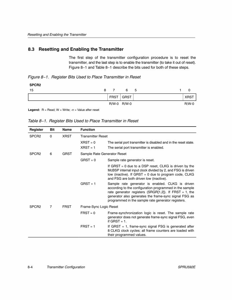
Resetting and Enabling the Transmitter
Transmitter Configuration8-4 SPRU592E
8.3 Resetting and Enabling the Transmitter
The first step of the transmitter configuration procedure is to reset thetransmitter, and the last step is to enable the transmitter (to take it out of reset).Figure 8−1 and Table 8−1 describe the bits used for both of these steps.
Figure 8−1. Register Bits Used to Place Transmitter in Reset
SPCR2
15 8 7 6 5 1 0
FRST GRST XRST
R/W-0 R/W-0 R/W-0
Legend: R = Read; W = Write; -n = Value after reset
Table 8−1. Register Bits Used to Place Transmitter in Reset
Register Bit Name Function
SPCR2 0 XRST Transmitter Reset
XRST = 0 The serial port transmitter is disabled and in the reset state.
XRST = 1 The serial port transmitter is enabled.
SPCR2 6 GRST Sample Rate Generator Reset
GRST = 0 Sample rate generator is reset.
If GRST = 0 due to a DSP reset, CLKG is driven by theMcBSP internal input clock divided by 2, and FSG is drivenlow (inactive). If GRST = 0 due to program code, CLKGand FSG are both driven low (inactive).
GRST = 1 Sample rate generator is enabled. CLKG is drivenaccording to the configuration programmed in the samplerate generator registers (SRGR[1,2]). If FRST = 1, thegenerator also generates the frame-sync signal FSG asprogrammed in the sample rate generator registers.
SPCR2 7 FRST Frame-Sync Logic Reset
FRST = 0 Frame-synchronization logic is reset. The sample rategenerator does not generate frame-sync signal FSG, evenif GRST = 1.
FRST = 1 If GRST = 1, frame-sync signal FSG is generated after8 CLKG clock cycles; all frame counters are loaded withtheir programmed values.
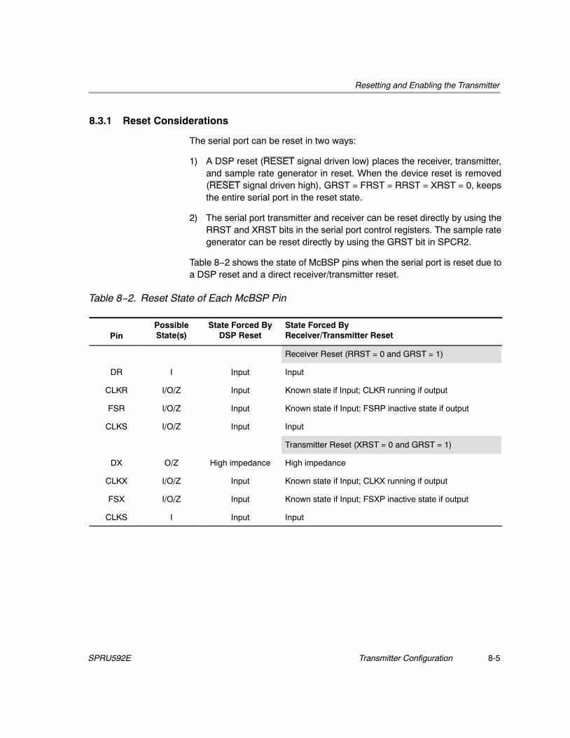
Resetting and Enabling the Transmitter
8-5Transmitter ConfigurationSPRU592E
8.3.1 Reset Considerations
The serial port can be reset in two ways:
1) A DSP reset (RESET signal driven low) places the receiver, transmitter,and sample rate generator in reset. When the device reset is removed(RESET signal driven high), GRST = FRST = RRST = XRST = 0, keepsthe entire serial port in the reset state.
2) The serial port transmitter and receiver can be reset directly by using theRRST and XRST bits in the serial port control registers. The sample rategenerator can be reset directly by using the GRST bit in SPCR2.
Table 8−2 shows the state of McBSP pins when the serial port is reset due toa DSP reset and a direct receiver/transmitter reset.
Table 8−2. Reset State of Each McBSP Pin
PinPossibleState(s)
State Forced ByDSP Reset
State Forced ByReceiver/Transmitter Reset
Receiver Reset (RRST = 0 and GRST = 1)
DR I Input Input
CLKR I/O/Z Input Known state if Input; CLKR running if output
FSR I/O/Z Input Known state if Input; FSRP inactive state if output
CLKS I/O/Z Input Input
Transmitter Reset (XRST = 0 and GRST = 1)
DX O/Z High impedance High impedance
CLKX I/O/Z Input Known state if Input; CLKX running if output
FSX I/O/Z Input Known state if Input; FSXP inactive state if output
CLKS I Input Input

Setting the Transmitter Pins to Operate as McBSP Pins
Transmitter Configuration8-6 SPRU592E
8.4 Setting the Transmitter Pins to Operate as McBSP Pins
Use the XIOEN bit, shown in Figure 8−2 and described in Table 8−3, to makethe transmitter pins operate as McBSP pins rather than I/O pins.
Figure 8−2. Register Bit Used to Set Transmitter Pins to Operate as McBSP Pins
PCR
15 14 13 12 0
XIOEN
R/W-0
Legend: R = Read; W = Write; -n = Value after reset
Table 8−3. Register Bit Used to Set Transmitter Pins to Operate as McBSP Pins
Register Bit Name Function
PCR 13 XIOEN Transmit I/O enable
This bit is only applicable when the transmitter is in the reset state (XRST = 0in SPCR2).
XIOEN = 0 The DX, FSX, CLKX, and CLKS pins are configured asserial port pins and do not function as general-purposeI/Os.
XIOEN = 1 The DX pin is a general-purpose output pin. The FSX andCLKX pins are general-purpose I/O pins. These serial portpins do not perform serial port operation. The CLKS pin isa general-purpose input pin if RIOEN = XIOEN = 1 andRRST = XRST = 0.

Enabling/Disabling the Digital Loopback Mode
8-7Transmitter ConfigurationSPRU592E
8.5 Enabling/Disabling the Digital Loopback Mode
The DLB bit determines whether the digital loopback mode is on. DLB is shownin Figure 8−3 and described in Table 8−4.
Figure 8−3. Register Bit Used to Enable/Disable the Digital Loopback Mode
SPCR1
15 14 0
DLB
R/W-0
Legend: R = Read; W = Write; -n = Value after reset
Table 8−4. Register Bit Used to Enable/Disable the Digital Loopback Mode
Register Bit Name Function
SPCR1 15 DLB Digital Loopback Mode
DLB = 0 Digital loopback mode is disabled.
DLB = 1 Digital loopback mode is enabled.
8.5.1 About the Digital Loopback Mode
In the digital loopback mode, the receive signals are connected internallythrough multiplexers to the corresponding transmit signals, as shown inTable 8−5. This mode allows testing of serial port code with a single DSPdevice; the McBSP receives the data it transmits.
Table 8−5. Receive Signals Connected to Transmit Signals in Digital Loopback Mode
This Receive Signal …Is Fed Internally ByThis Transmit Signal …
DR (receive data) DX (transmit data)
FSR (receive frame synchronization) FSX (transmit frame synchronization)
CLKR (receive clock) CLKX (transmit clock)

Enabling/Disabling the Clock Stop Mode
Transmitter Configuration8-8 SPRU592E
8.6 Enabling/Disabling the Clock Stop Mode
The CLKSTP bits determine whether the clock stop mode is on and whethera clock delay is selected. CLKSTP is shown in Figure 8−4 and described inTable 8−6.
Figure 8−4. Register Bits Used to Enable/Disable the Clock Stop Mode
SPCR1
15 13 12 11 10 0
CLKSTP
R/W-00
Legend: R = Read; W = Write; -n = Value after reset
Table 8−6. Register Bits Used to Enable/Disable the Clock Stop Mode
Register Bit Name Function
SPCR1 12-11 CLKSTP Clock Stop Mode
CLKSTP = 0Xb Clock stop mode disabled; normal clocking for non-SPImode.
CLKSTP = 10b Clock stop mode enabled, without clock delay
CLKSTP = 11b Clock stop mode enabled, with clock delay
8.6.1 About the Clock Stop Mode
The clock stop mode supports the SPI master-slave protocol. If you are notusing the SPI protocol, you can clear CLKSTP to disable the clock stop mode.
In the clock stop mode, the clock stops at the end of each data transfer. At thebeginning of each data transfer, the clock starts immediately (CLKSTP = 10b)or after a half-cycle delay (CLKSTP = 11b). The CLKXP bit determineswhether the starting edge of the clock on the CLKX pin is rising or falling. TheCLKRP bit determines whether receive data is sampled on the rising or fallingedge of the clock shown on the CLKR pin.
Table 6−2, on page 6-5, summarizes the impact of CLKSTP, CLKXP, andCLKRP on serial port operation. Note that in the clock stop mode, the receiveclock is tied internally to the transmit clock, and the receive frame-sync signalis tied internally to the transmit frame-sync signal.

Enabling/Disabling Transmit Multichannel Selection
8-9Transmitter ConfigurationSPRU592E
8.7 Enabling/Disabling Transmit Multichannel Selection
The XMCM bits, shown in Figure 8−5 and described in Table 8−7, are used toselect one of the three transmit multichannel selection modes, or to disabletransmit multichannel selection.
Figure 8−5. Register Bits Used to Enable/Disable Transmit Multichannel Selection
MCR2
15 2 1 0
XMCM
R/W-00
Legend: R = Read; W = Write; -n = Value after reset
Table 8−7. Register Bits Used to Enable/Disable Transmit Multichannel Selection
Register Bit Name Function
MCR2 1-0 XMCM Transmit Multichannel Selection
XMCM = 00b Transmit multichannel selection is off. All channels areenabled and unmasked. No channels can be disabled ormasked.
XMCM = 01b All channels are disabled unless they are selected in theappropriate transmit channel enable registers (XCERs). Ifenabled, a channel in this mode is also unmasked.
The XMCME bit determines whether 32 channels or128 channels are selectable in XCERs.
XMCM = 10b All channels are enabled, but they are masked unless theyare selected in the appropriate transmit channel enableregisters (XCERs).
The XMCME bit determines whether 32 channels or128 channels are selectable in XCERs.
XMCM = 11b This mode is used for symmetric transmission andreception.
All channels are disabled for transmission unless they areenabled for reception in the appropriate receive channelenable registers (RCERs). Once enabled, they are maskedunless they are also selected in the appropriate transmitchannel enable registers (XCERs).
The XMCME bit determines whether 32 channels or128 channels are selectable in RCERs and XCERs.
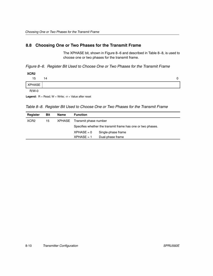
Choosing One or Two Phases for the Transmit Frame
Transmitter Configuration8-10 SPRU592E
8.8 Choosing One or Two Phases for the Transmit Frame
The XPHASE bit, shown in Figure 8−6 and described in Table 8−8, is used tochoose one or two phases for the transmit frame.
Figure 8−6. Register Bit Used to Choose One or Two Phases for the Transmit Frame
XCR2
15 14 0
XPHASE
R/W-0
Legend: R = Read; W = Write; -n = Value after reset
Table 8−8. Register Bit Used to Choose One or Two Phases for the Transmit Frame
Register Bit Name Function
XCR2 15 XPHASE Transmit phase number
Specifies whether the transmit frame has one or two phases.
XPHASE = 0 Single-phase frame
XPHASE = 1 Dual-phase frame

Setting the Transmit Word Length(s)
8-11Transmitter ConfigurationSPRU592E
8.9 Setting the Transmit Word Length(s)
The XWDLEN1 an XWDLEN2 fields (see Figure 8−7 and Table 8−9) are usedto set the transmit word length(s).
Figure 8−7. Register Bits Used to Set the Transmit Word Length(s)
XCR1
15 8 7 5 4 0
XWDLEN1
R/W-000XCR2
15 8 7 5 4 0
XWDLEN2
R/W-000
Legend: R = Read; W = Write; -n = Value after reset
Table 8−9. Register Bits Used to Set the Transmit Word Length(s)
Register Bit Name Function
XCR1 7-5 XWDLEN1 Transmit Word Length of Frame Phase 1
XWDLEN1 = 000b 8 bits
XWDLEN1 = 001b 12 bits
XWDLEN1 = 010b 16 bits
XWDLEN1 = 011b 20 bits
XWDLEN1 = 100b 24 bits
XWDLEN1 = 101b 32 bits
XWDLEN1 = 11Xb Reserved
XCR2 7-5 XWDLEN2 Transmit Word Length of Frame Phase 2
XWDLEN2 = 000b 8 bits
XWDLEN2 = 001b 12 bits
XWDLEN2 = 010b 16 bits
XWDLEN2 = 011b 20 bits
XWDLEN2 = 100b 24 bits
XWDLEN2 = 101b 32 bits
XWDLEN2 = 11Xb Reserved

Setting the Transmit Word Length(s)
Transmitter Configuration8-12 SPRU592E
8.9.1 About the Word Length Bits
Each frame can have one or two phases, depending on the value that you loadinto the XPHASE bit. If a single-phase frame is selected, XWDLEN1 selectsthe length for every serial word transmitted in the frame. If a dual-phase frameis selected, XWDLEN1 determines the length of the serial words in phase 1of the frame, and XWDLEN2 determines the word length in phase 2 of theframe.

Setting the Transmit Frame Length
8-13Transmitter ConfigurationSPRU592E
8.10 Setting the Transmit Frame Length
The XFRLEN1 and XFRLEN2 fields (see Figure 8−8 and Table 8−10) areused to set the transmit frame length.
Figure 8−8. Register Bits Used to Set the Transmit Frame Length
XCR1
15 14 8 7 0
XFRLEN1
R/W-000 0000XCR2
15 14 8 7 0
XFRLEN2
R/W-000 0000
Legend: R = Read; W = Write; -n = Value after reset
Table 8−10. Register Bits Used to Set the Transmit Frame Length
Register Bit Name Function
XCR1 14-8 XFRLEN1 Transmit frame length 1
(XFRLEN1 + 1) is the number of serial words in phase 1 of the transmit frame.
XFRLEN1 = 000 0000 1 word in phase 1
XFRLEN1 = 000 0001 2 words in phase 1
| |
| |
XFRLEN1 = 111 1111 128 words in phase 1
XCR2 14-8 XFRLEN2 Transmit frame length 2
If a dual-phase frame is selected, (XFRLEN2 + 1) is the number of serialwords in phase 2 of the transmit frame.
XFRLEN2 = 000 0000 1 word in phase 2
XFRLEN2 = 000 0001 2 words in phase 2
| |
| |
XFRLEN2 = 111 1111 128 words in phase 2

Setting the Transmit Frame Length
Transmitter Configuration8-14 SPRU592E
8.10.1 About the Selected Frame Length
The transmit frame length is the number of serial words in the transmit frame.Each frame can have one or two phases, depending on value that you load intothe XPHASE bit.
If a single-phase frame is selected (XPHASE = 0), the frame length is equalto the length of phase 1. If a dual-phase frame is selected (XPHASE = 1), theframe length is the length of phase 1 plus the length of phase 2.
The 7-bit XFRLEN fields allow up to 128 words per phase. See Table 8−11 fora summary of how to calculate the frame length. This length corresponds tothe number of words or logical time slots or channels perframe-synchronization pulse.
Note: Program the XFRLEN fields with [w minus 1], where w represents thenumber of words per phase. For the example, if you want a phase length of128 words in phase 1, load 127 into XFRLEN1.
Table 8−11. How to Calculate Frame Length
XPHASE XFRLEN1 XFRLEN2 Frame Length
0 0 ≤ XFRLEN1 ≤ 127 Don’t care (XFRLEN1 + 1) words
1 0 ≤ XFRLEN1 ≤ 127 0 ≤ XFRLEN2 ≤ 127 (XFRLEN1 + 1) + (XFRLEN2 + 1) words

Enabling/Disabling the Transmit Frame-Sync Ignore Function
8-15Transmitter ConfigurationSPRU592E
8.11 Enabling/Disabling the Transmit Frame-Sync Ignore Function
The XFIG bit (see Figure 8−9 and Table 8−12) determines whetherunexpected frame sync-pulses are ignored during transmission.
Figure 8−9. Register Bit Used to Enable/Disable the Transmit Frame-SyncIgnore Function
XCR2
15 3 2 1 0
XFIG
R/W-0
Legend: R = Read; W = Write; -n = Value after reset
Table 8−12. Register Bit Used to Enable/Disable the Transmit Frame-Sync IgnoreFunction
Register Bit Name Function
XCR2 2 XFIG Transmit Frame-Sync Ignore
XFIG = 0 An unexpected transmit frame-sync pulse causes theMcBSP to restart the frame transfer.
XFIG = 1 The McBSP ignores unexpected transmit frame-syncpulses.
8.11.1 About Unexpected Frame-Sync Pulses and the Frame-Sync Ignore Function
If a frame-synchronization (frame-sync) pulse starts the transfer of a newframe before the current frame is fully transmitted, this pulse is treated as anunexpected frame-sync pulse.
When XFIG = 1, normal transmission continues with unexpected frame-syncsignals ignored.
When XFIG = 0 and an unexpected frame-sync pulse occurs, the serial port:
1) Aborts the present transmission
2) Sets XSYNCERR to 1 in SPCR2
3) Re-initiates transmission of the current word that was aborted

Setting the Transmit Companding Mode
Transmitter Configuration8-16 SPRU592E
8.12 Setting the Transmit Companding Mode
The XCOMPAND field, shown in Figure 8−10 and described in Table 8−13,determine whether companding or another data transfer option is chosen forMcBSP transmission.
Figure 8−10. Register Bits Used to Set the Transmit Companding Mode
XCR2
15 5 4 3 2 0
XCOMPAND
R/W-00
Legend: R = Read; W = Write; -n = Value after reset
Table 8−13. Register Bits Used to Set the Transmit Companding Mode
Register Bit Name Function
XCR2 4-3 XCOMPAND Transmit Companding Mode
Modes other than 00b are enabled only when the appropriate XWDLEN is000b, indicating 8-bit data.
XCOMPAND = 00b No companding, any size data, MSB transmittedfirst
XCOMPAND = 01b No companding, 8-bit data, LSB transmitted first(for details, scroll down to Option to Transmit LSBFirst)
XCOMPAND = 10b µ-law companding, 8-bit data, MSB transmittedfirst
XCOMPAND = 11b A-law companding, 8-bit data, MSB transmittedfirst
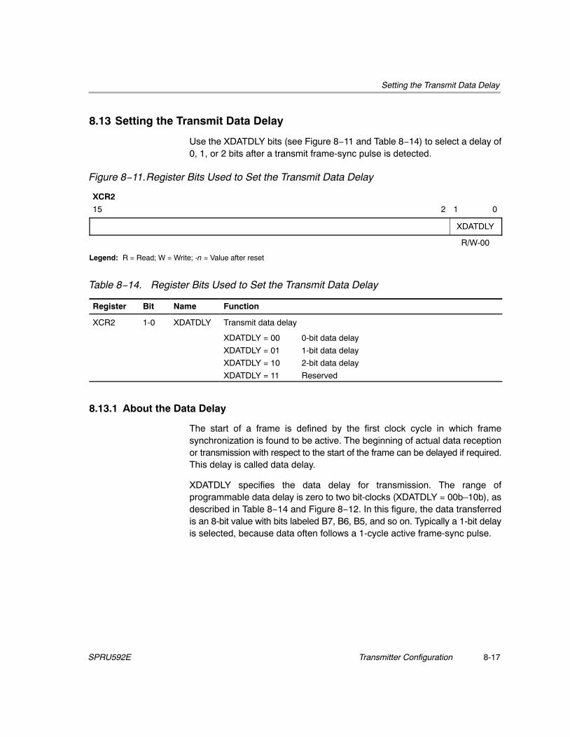
Setting the Transmit Data Delay
8-17Transmitter ConfigurationSPRU592E
8.13 Setting the Transmit Data Delay
Use the XDATDLY bits (see Figure 8−11 and Table 8−14) to select a delay of0, 1, or 2 bits after a transmit frame-sync pulse is detected.
Figure 8−11.Register Bits Used to Set the Transmit Data Delay
XCR2
15 2 1 0
XDATDLY
R/W-00
Legend: R = Read; W = Write; -n = Value after reset
Table 8−14. Register Bits Used to Set the Transmit Data Delay
Register Bit Name Function
XCR2 1-0 XDATDLY Transmit data delay
XDATDLY = 00 0-bit data delay
XDATDLY = 01 1-bit data delay
XDATDLY = 10 2-bit data delay
XDATDLY = 11 Reserved
8.13.1 About the Data Delay
The start of a frame is defined by the first clock cycle in which framesynchronization is found to be active. The beginning of actual data receptionor transmission with respect to the start of the frame can be delayed if required.This delay is called data delay.
XDATDLY specifies the data delay for transmission. The range ofprogrammable data delay is zero to two bit-clocks (XDATDLY = 00b–10b), asdescribed in Table 8−14 and Figure 8−12. In this figure, the data transferredis an 8-bit value with bits labeled B7, B6, B5, and so on. Typically a 1-bit delayis selected, because data often follows a 1-cycle active frame-sync pulse.

Setting the Transmit Data Delay
Transmitter Configuration8-18 SPRU592E
Figure 8−12. Range of Programmable Data Delay
B5B6B7
B4B5B6B7
B3B4B5B6B7
Data delay 2D(R/X)
Data delay 1D(R/X)
Data delay 0D(R/X)
FS(R/X)
CLK(R/X)
1-bit delay
ÁÁ
ÁÁ
ÁÁ
0-bit delay
2-bit delay
8.13.2 0-Bit Data Delay
Normally, a frame-sync pulse is detected or sampled with respect to an edgeof serial clock internal CLK(R/X). Therefore, on the following cycle or later(depending on the data delay value), data may be received or transmitted.However, in the case of 0-bit data delay, the data must be ready for receptionand/or transmission on the same serial clock cycle.
For reception, this problem is solved because receive data is sampled on thefirst falling edge of CLKR where an active-high internal FSR is detected.However, data transmission must begin on the rising edge of the internal CLKXclock that generated the frame synchronization. Therefore, the first data bit isassumed to be present in XSR1, and thus on DX. The transmitter thenasynchronously detects the frame synchronization, FSX, going active high,and immediately starts driving the first bit to be transmitted on the DX pin.
8.13.3 2-Bit Data Delay
A data delay of two bit periods allows the serial port to interface to differenttypes of T1 framing devices where the data stream is preceded by a framingbit. During reception of such a stream with data delay of two bits (framing bitappears after a 1-bit delay and data appears after a 2-bit delay), the serial portessentially discards the framing bit from the data stream, as shownFigure 8−13. In this figure, the data transferred is an 8-bit value with bitslabeled B7, B6, B5, and so on.

Setting the Transmit Data Delay
8-19Transmitter ConfigurationSPRU592E
Figure 8−13. 2-Bit Data Delay Used to Skip a Framing Bit
DR Framing bit B5B6B7
FSR
CLKR
ÁÁ
2-bit delay

Setting the Transmit DXENA Mode
Transmitter Configuration8-20 SPRU592E
8.14 Setting the Transmit DXENA Mode
The DXENA bit (see Figure 8−14 and Table 8−15) controls the delay enableron the DX pin.
Figure 8−14. Register Bit Used to Set the Transmit DXENA (DX Delay Enabler) Mode
SPCR1
15 8 7 6 0
DXENA
R/W-0
Legend: R = Read; W = Write; -n = Value after reset
Table 8−15. Register Bit Used to Set the Transmit DXENA (DX Delay Enabler) Mode
Register Bit Name Function
SPCR1 7 DXENA DX Delay Enabler Mode
DXENA = 0 DX delay enabler is off.
DXENA = 1 DX delay enabler is on.
8.14.1 About the DXENA Mode
The DXENA bit controls the delay enabler on the DX pin. Set DXENA to enablean extra delay for turn-on time (for the length of the delay for a particular C55xdevice, see the device-specific data manual). Note that this bit does not controlthe data itself, so only the first bit is delayed.
If you tie together the DX pins of multiple McBSPs, make sure DXENA = 1 toavoid having more than one McBSP transmit on the data line at one time.
Figure 8−15 shows the timing of the DX pin for DXENA = 1.
Figure 8−15. DX Delay When DXENA = 1
te
CLKX
FSX
DX
Note: te = extra delay for turn on time with DXENA = 1

Setting the Transmit Interrupt Mode
8-21Transmitter ConfigurationSPRU592E
8.15 Setting the Transmit Interrupt Mode
Use the XINTM field to select which event generates a transmit interrupt.XINTM is shown in Figure 8−16 and described in Table 8−16.
Figure 8−16. Register Bits Used to Set the Transmit Interrupt Mode
SPCR2
15 6 5 4 3 0
XINTM
R/W-00
Legend: R = Read; W = Write; -n = Value after reset
Table 8−16. Register Bits Used to Set the Transmit Interrupt Mode
Register Bit Name Function
SPCR2 5-4 XINTM Transmit Interrupt Mode
XINTM = 00 XINT generated when XRDY changes from 0 to 1
XINTM = 01 XINT generated by an end-of-block or end-of-framecondition in a transmit multichannel selection mode
XINTM = 10 XINT generated by a new transmit frame-sync pulse
XINTM = 11 XINT generated when XSYNCERR is set
8.15.1 About the Transmitter Interrupt and the Associated Modes
The transmitter interrupt (XINT) signals the CPU of changes to the serial portstatus. Four options exist for configuring this interrupt. The options are set bythe transmit interrupt mode bits, XINTM, in SPCR2.
� XINTM = 00b. Interrupt on every serial word by tracking the XRDY bit inSPCR2. Note that regardless of the value of XINTM, XRDY can be readto detect the XRDY = 1 condition.
� XINTM = 01b. In any of the transmit multichannel selection modes,interrupt after every 16-channel block boundary has been crossed withina frame and at the end of the frame. In any other serial transfer case, thissetting is not applicable and, therefore, no interrupts are generated.
� XINTM = 10b. Interrupt on detection of each transmit frame-sync pulse.This generates an interrupt even when the transmitter is in its reset state.This is done by synchronizing the incoming frame-sync pulse to theMcBSP internal input clock and sending it to the CPU via XINT.
� XINTM = 11b. Interrupt on frame-synchronization error. Note thatregardless of the value of XINTM, XSYNCERR can be read to detect thiscondition.

Setting the Transmit Frame-Sync Mode
Transmitter Configuration8-22 SPRU592E
8.16 Setting the Transmit Frame-Sync Mode
The bits shown in Figure 8−17 and Table 8−17 are used to set the transmitframe-sync mode.
Figure 8−17. Register Bits Used to Set the Transmit Frame-Sync Mode
PCR
15 12 11 10 0
FSXM
R/W-0SRGR2
15 13 12 11 0
FSGM
R/W-0
Legend: R = Read; W = Write; -n = Value after reset
Table 8−17. Register Bits Used to Set the Transmit Frame-Sync Mode
Register Bit Name Function
PCR 11 FSXM Transmit Frame-Synchronization Mode
FSXM = 0 Transmit frame synchronization is supplied by an externalsource via the FSX pin.
FSXM = 1 Transmit frame synchronization is supplied by the McBSP,as determined by the FSGM bit of SRGR2.
SRGR2 12 FSGM Sample Rate Generator Transmit Frame-Synchronization Mode
Used when FSXM = 1 in PCR.
FSGM = 0 The McBSP generates a transmit frame-sync pulse whenthe content of DXR[1,2] is copied to XSR[1,2].
FSGM = 1 The transmitter uses frame-sync pulses generated by thesample rate generator. Program the FWID bits to set thewidth of each pulse. Program the FPER bits to set theframe-sync period.
8.16.1 About the Transmit Frame-Sync Modes
Table 8−18 shows how FSXM and FSGM select the source of transmitframe-sync pulses. The three choices are:
� External frame-sync input
� Sample rate generator frame-sync signal (FSG)
� Internal signal that indicates a DXR-to-XSR copy has been made

Setting the Transmit Frame-Sync Mode
8-23Transmitter ConfigurationSPRU592E
Table 8−18 also shows the effect of each bit setting on the FSX pin. Thepolarity of the signal on the FSX pin is determined by the FSXP bit.
Table 8−18. How FSXM and FSGM Select the Source of Transmit Frame-Sync Pulses
FSXM FSGMSource of Transmit FrameSynchronization FSX Pin Status
0 0 or 1 An external frame-sync signal enters theMcBSP through the FSX pin. The signal isthen inverted by FSXP before being usedas internal FSX.
Input
1 1 Internal FSX is driven by the sample rategenerator frame-sync signal (FSG).
Output. FSG is inverted by FSXP beforebeing driven out on FSX pin.
1 0 A DXR-to-XSR copy causes the McBSP togenerate a transmit frame-sync pulse thatis 1 cycle wide.
Output. The generated frame-sync pulse isinverted as determined by FSXP beforebeing driven out on FSX pin.
8.16.2 Other Considerations
If the sample rate generator creates a frame-sync signal (FSG) that is derivedfrom an external input clock, the GSYNC bit determines whether FSG is keptsynchronized with pulses on the FSR pin.
In the clock stop mode (CLKSTP = 10b or 11b), the McBSP can act as amaster or as a slave in the SPI protocol. If the McBSP is a master and mustprovide a slave-enable signal (SS) on the FSX pin, make sure that FSXM = 1and FSGM = 0, so that FSX is an output and is driven active for the durationof each transmission. If the McBSP is a slave, make sure that FSXM = 0, sothat the McBSP can receive the slave-enable signal on the FSX pin.

Setting the Transmit Frame-Sync Polarity
Transmitter Configuration8-24 SPRU592E
8.17 Setting the Transmit Frame-Sync Polarity
The FSXP bit (see Figure 8−18 and Table 8−19) determines the polarity of thetransmit frame-sync signal.
Figure 8−18. Register Bit Used to Set Transmit Frame-Sync Polarity
PCR
15 4 3 2 0
FSXP
R/W-0
Legend: R = Read; W = Write; -n = Value after reset
Table 8−19. Register Bit Used to Set Transmit Frame-Sync Polarity
Register Bit Name Function
PCR 3 FSXP Transmit Frame-Synchronization Polarity
FSXP = 0 Frame-synchronization pulse FSX is active high.
FSXP = 1 Frame-synchronization pulse FSX is active low.
8.17.1 About Frame Sync Pulses, Clock Signals, and Their Polarities
Transmit frame-sync pulses can be either generated internally by the samplerate generator or driven by an external source. The source of frame sync isselected by programming the mode bit, FSXM, in PCR. FSX is also affectedby the FSGM bit in SRGR2. Similarly, transmit clocks can be selected to beinputs or outputs by programming the mode bit, CLKXM, in the PCR.
When FSR and FSX are inputs (FSXM = FSRM= 0, external frame-syncpulses), the McBSP detects them on the internal falling edge of clock, internalCLKR, and internal CLKX, respectively. The receive data arriving at the DR pinis also sampled on the falling edge of internal CLKR. Note that these internalclock signals are either derived from external source via CLK(R/X) pins ordriven by the sample rate generator clock (CLKG) internal to the McBSP.
When FSR and FSX are outputs, implying that they are driven by the samplerate generator, they are generated (transition to their active state) on the risingedge of internal clock, CLK(R/X). Similarly, data on the DX pin is output on therising edge of internal CLKX.

Setting the Transmit Frame-Sync Polarity
8-25Transmitter ConfigurationSPRU592E
FSRP, FSXP, CLKRP, and CLKXP in the pin control register (PCR) configurethe polarities of the FSR, FSX, CLKR, and CLKX signals, respectively. Allframe-sync signals (internal FSR, internal FSX) that are internal to the serialport are active high. If the serial port is configured for external framesynchronization (FSR/FSX are inputs to McBSP), and FSRP = FSXP = 1, theexternal active-low frame-sync signals are inverted before being sent to thereceiver (internal FSR) and transmitter (internal FSX). Similarly, if internalsynchronization (FSR/FSX are output pins and GSYNC = 0) is selected, theinternal active-high frame-sync signals are inverted, if the polarity bitFS(R/X)P = 1, before being sent to the FS(R/X) pin.
On the transmit side, the transmit clock polarity bit, CLKXP, sets the edge usedto shift and clock out transmit data. Note that data is always transmitted on therising edge of internal CLKX. If CLKXP = 1, and external clocking is selected(CLKXM = 0 and CLKX is an input), the external falling-edge triggered inputclock on CLKX is inverted to a rising-edge triggered clock before being sentto the transmitter. If CLKXP = 1, and internal clocking selected (CLKXM = 1and CLKX is an output pin), the internal (rising-edge triggered) clock, internalCLKX, is inverted before being sent out on the CLKX pin.
Similarly, the receiver can reliably sample data that is clocked with a risingedge clock (by the transmitter). The receive clock polarity bit, CLKRP, sets theedge used to sample received data. Note that the receive data is alwayssampled on the falling edge of internal CLKR. Therefore, if CLKRP = 1 andexternal clocking is selected (CLKRM = 0 and CLKR is an input pin), theexternal rising-edge triggered input clock on CLKR is inverted to a falling-edgetriggered clock before being sent to the receiver. If CLKRP = 1, and internalclocking is selected (CLKRM = 1), the internal falling-edge triggered clock isinverted to a rising-edge triggered clock before being sent out on the CLKR pin.
Note that CLKRP = CLKXP in a system where the same clock (internal orexternal) is used to clock the receiver and transmitter. The receiver uses theopposite edge as the transmitter to ensure valid setup and hold of data aroundthis edge. Figure 8−19 shows how data clocked by an external serial deviceusing a rising edge can be sampled by the McBSP receiver on the falling edgeof the same clock.

Setting the Transmit Frame-Sync Polarity
Transmitter Configuration8-26 SPRU592E
Figure 8−19. Data Clocked Externally Using a Rising Edge andSampled by the McBSP Receiver on a Falling Edge
B6B7DR
CLKR
Data hold
ÁÁÁÁ
Data setup
Internal

Setting the SRG Frame-Sync Period and Pulse Width
8-27Transmitter ConfigurationSPRU592E
8.18 Setting the SRG Frame-Sync Period and Pulse Width
The FPER and FWID fields, shown in Figure 8−20 and described inTable 8−20, are used to set the SRG frame-sync period and pulse width.
Figure 8−20. Register Bits Used to Set the SRG Frame-Sync Period and Pulse Width
SRGR2
15 12 11 0
FPER
R/W-0000 0000 0000SRGR1
15 8 7 0
FWID
R/W-0000 0000
Legend: R = Read; W = Write; -n = Value after reset
Table 8−20. Register Bits Used to Set the SRG Frame-Sync Period and Pulse Width
Register Bit Name Function
SRGR2 11-0 FPER Sample Rate Generator Frame-Sync Period
For the frame-sync signal FSG, (FPER + 1) determines the period from thestart of a frame-sync pulse to the start of the next frame-sync pulse.
Range for (FPER + 1): 1 to 4096 CLKG cycles.
SRGR1 15-8 FWID Sample Rate Generator Frame-Sync Pulse Width
This field plus 1 determines the width of each frame-sync pulse on FSG.
Range for (FWID + 1): 1 to 256 CLKG cycles.
8.18.1 About the Frame-Sync Period and the Frame-Sync Pulse Width
The sample rate generator can produce a clock signal, CLKG, and aframe-sync signal, FSG. If the sample rate generator is supplying receive ortransmit frame synchronization, you must program the bit fields FPER andFWID.
On FSG, the period from the start of a frame-sync pulse to the start of the nextpulse is (FPER + 1) CLKG cycles. The 12 bits of FPER allow a frame-syncperiod of 1 to 4096 CLKG cycles, which allows up to 4096 data bits per frame.When GSYNC = 1, FPER is a don’t care value.
Each pulse on FSG has a width of (FWID + 1) CLKG cycles. The eight bits ofFWID allow a pulse width of 1 to 256 CLKG cycles. It is recommended thatFWID be programmed to a value less than the programmed word length.

Setting the SRG Frame-Sync Period and Pulse Width
Transmitter Configuration8-28 SPRU592E
The values in FPER and FWID are loaded into separate down-counters. The12-bit FPER counter counts down the generated clock cycles from theprogrammed value (4095 maximum) to 0. The 8-bit FWID counter countsdown from the programmed value (255 maximum) to 0.
Figure 8−21 shows a frame-sync period of 16 CLKG periods(FPER = 15 or 00001111b) and a frame-sync pulse with an active width of2 CLKG periods (FWID = 1).
Figure 8−21. Frame of Period 16 CLKG Periods and Active Width of 2 CLKG Periods
FSG
CLKG
19181716151413121110987654321
Frame-sync period: (FPER+1) x CLKG
Frame-sync pulse width: (FWID + 1) x CLKG
When the sample rate generator comes out of reset, FSG is in its inactive state.Then, when FRST = 1 and FSGM = 1, a frame-sync pulse is generated. Theframe width value (FWID + 1) is counted down on every CLKG cycle until itreaches 0, at which time FSG goes low. At the same time, the frame periodvalue (FPER + 1) is also counting down. When this value reaches 0, FSG goeshigh, indicating a new frame.
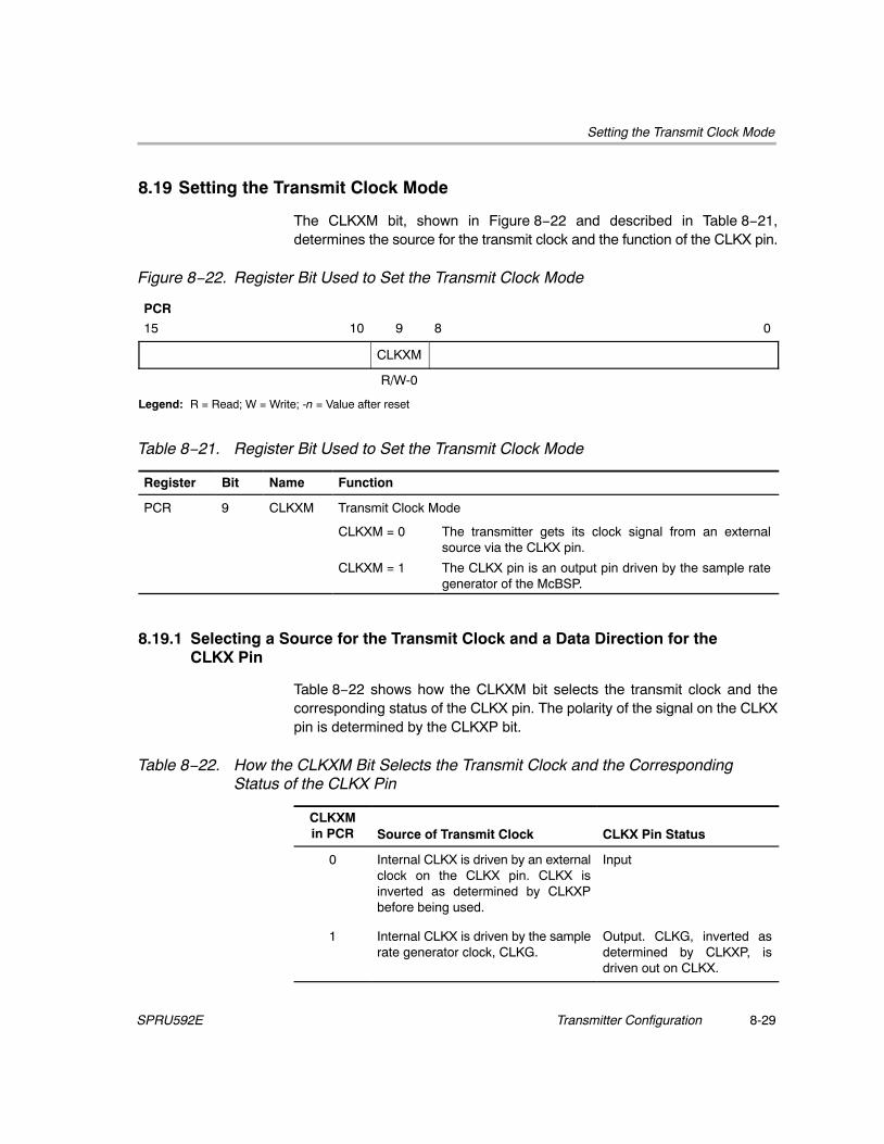
Setting the Transmit Clock Mode
8-29Transmitter ConfigurationSPRU592E
8.19 Setting the Transmit Clock Mode
The CLKXM bit, shown in Figure 8−22 and described in Table 8−21,determines the source for the transmit clock and the function of the CLKX pin.
Figure 8−22. Register Bit Used to Set the Transmit Clock Mode
PCR
15 10 9 8 0
CLKXM
R/W-0
Legend: R = Read; W = Write; -n = Value after reset
Table 8−21. Register Bit Used to Set the Transmit Clock Mode
Register Bit Name Function
PCR 9 CLKXM Transmit Clock Mode
CLKXM = 0 The transmitter gets its clock signal from an externalsource via the CLKX pin.
CLKXM = 1 The CLKX pin is an output pin driven by the sample rategenerator of the McBSP.
8.19.1 Selecting a Source for the Transmit Clock and a Data Direction for theCLKX Pin
Table 8−22 shows how the CLKXM bit selects the transmit clock and thecorresponding status of the CLKX pin. The polarity of the signal on the CLKXpin is determined by the CLKXP bit.
Table 8−22. How the CLKXM Bit Selects the Transmit Clock and the CorrespondingStatus of the CLKX Pin
CLKXMin PCR Source of Transmit Clock CLKX Pin Status
0 Internal CLKX is driven by an externalclock on the CLKX pin. CLKX isinverted as determined by CLKXPbefore being used.
Input
1 Internal CLKX is driven by the samplerate generator clock, CLKG.
Output. CLKG, inverted asdetermined by CLKXP, isdriven out on CLKX.

Setting the Transmit Clock Mode
Transmitter Configuration8-30 SPRU592E
8.19.2 Other Considerations
If the sample rate generator creates a clock signal (CLKG) that is derived froman external input clock, the GSYNC bit determines whether CLKG is keptsynchronized with pulses on the FSR pin.
In the clock stop mode (CLKSTP = 10b or 11b), the McBSP can act as amaster or as a slave in the SPI protocol. If the McBSP is a master, make surethat CLKXM = 1, so that CLKX is an output to supply the master clock to anyslave devices. If the McBSP is a slave, make sure that CLKXM = 0, so thatCLKX is an input to accept the master clock signal.
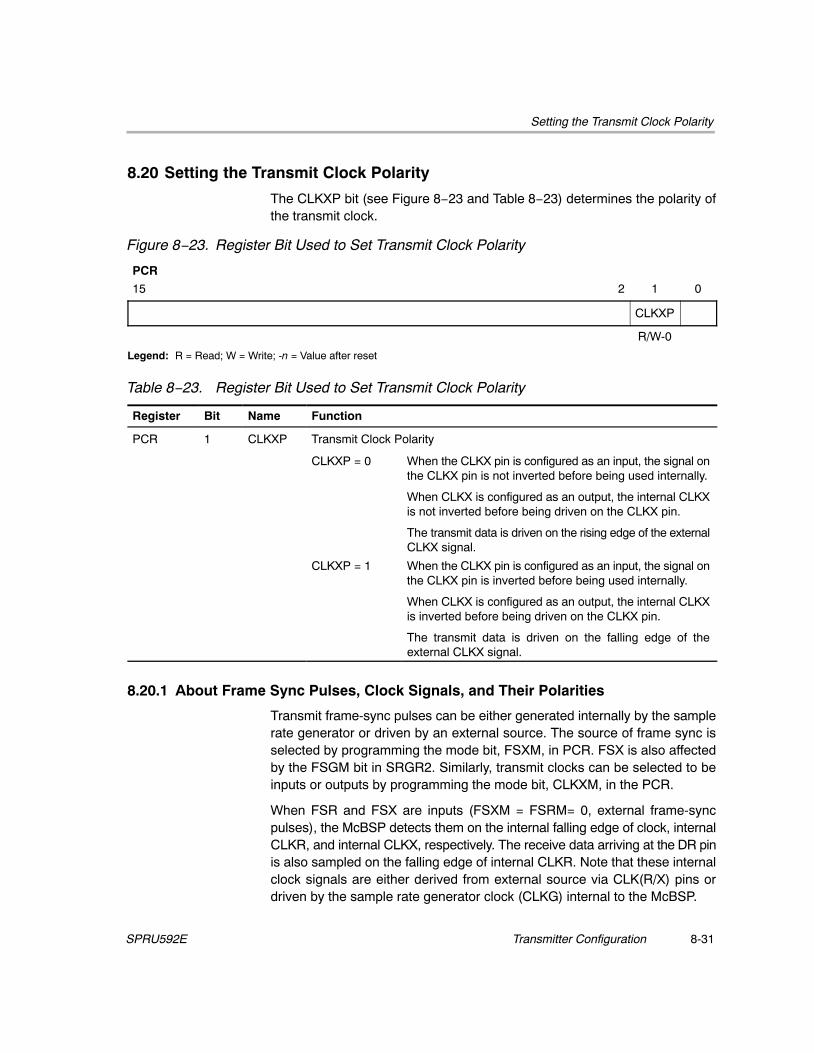
Setting the Transmit Clock Polarity
8-31Transmitter ConfigurationSPRU592E
8.20 Setting the Transmit Clock Polarity
The CLKXP bit (see Figure 8−23 and Table 8−23) determines the polarity ofthe transmit clock.
Figure 8−23. Register Bit Used to Set Transmit Clock Polarity
PCR
15 2 1 0
CLKXP
R/W-0
Legend: R = Read; W = Write; -n = Value after reset
Table 8−23. Register Bit Used to Set Transmit Clock Polarity
Register Bit Name Function
PCR 1 CLKXP Transmit Clock Polarity
CLKXP = 0 When the CLKX pin is configured as an input, the signal onthe CLKX pin is not inverted before being used internally.
When CLKX is configured as an output, the internal CLKXis not inverted before being driven on the CLKX pin.
The transmit data is driven on the rising edge of the externalCLKX signal.
CLKXP = 1 When the CLKX pin is configured as an input, the signal onthe CLKX pin is inverted before being used internally.
When CLKX is configured as an output, the internal CLKXis inverted before being driven on the CLKX pin.
The transmit data is driven on the falling edge of theexternal CLKX signal.
8.20.1 About Frame Sync Pulses, Clock Signals, and Their Polarities
Transmit frame-sync pulses can be either generated internally by the samplerate generator or driven by an external source. The source of frame sync isselected by programming the mode bit, FSXM, in PCR. FSX is also affectedby the FSGM bit in SRGR2. Similarly, transmit clocks can be selected to beinputs or outputs by programming the mode bit, CLKXM, in the PCR.
When FSR and FSX are inputs (FSXM = FSRM= 0, external frame-syncpulses), the McBSP detects them on the internal falling edge of clock, internalCLKR, and internal CLKX, respectively. The receive data arriving at the DR pinis also sampled on the falling edge of internal CLKR. Note that these internalclock signals are either derived from external source via CLK(R/X) pins ordriven by the sample rate generator clock (CLKG) internal to the McBSP.

Setting the Transmit Clock Polarity
Transmitter Configuration8-32 SPRU592E
When FSR and FSX are outputs, implying that they are driven by the samplerate generator, they are generated (transition to their active state) on the risingedge of internal clock, CLK(R/X). Similarly, data on the DX pin is output on therising edge of internal CLKX.
FSRP, FSXP, CLKRP, and CLKXP in the pin control register (PCR) configurethe polarities of the FSR, FSX, CLKR, and CLKX signals, respectively. Allframe-sync signals (internal FSR, internal FSX) that are internal to the serialport are active high. If the serial port is configured for external framesynchronization (FSR/FSX are inputs to McBSP), and FSRP = FSXP = 1, theexternal active-low frame-sync signals are inverted before being sent to thereceiver (internal FSR) and transmitter (internal FSX). Similarly, if internalsynchronization (FSR/FSX are output pins and GSYNC = 0) is selected, theinternal active-high frame-sync signals are inverted, if the polarity bitFS(R/X)P = 1, before being sent to the FS(R/X) pin.
On the transmit side, the transmit clock polarity bit, CLKXP, sets the edge usedto shift and clock out transmit data. Note that data is always transmitted on therising edge of internal CLKX. If CLKXP = 1, and external clocking is selected(CLKXM = 0 and CLKX is an input), the external falling-edge triggered inputclock on CLKX is inverted to a rising-edge triggered clock before being sentto the transmitter. If CLKXP = 1, and internal clocking selected (CLKXM = 1and CLKX is an output pin), the internal (rising-edge triggered) clock, internalCLKX, is inverted before being sent out on the CLKX pin.
Similarly, the receiver can reliably sample data that is clocked with a risingedge clock (by the transmitter). The receive clock polarity bit, CLKRP, sets theedge used to sample received data. Note that the receive data is alwayssampled on the falling edge of internal CLKR. Therefore, if CLKRP = 1 andexternal clocking is selected (CLKRM = 0 and CLKR is an input pin), theexternal rising-edge triggered input clock on CLKR is inverted to a falling-edgetriggered clock before being sent to the receiver. If CLKRP = 1, and internalclocking is selected (CLKRM = 1), the internal falling-edge triggered clock isinverted to a rising-edge triggered clock before being sent out on the CLKR pin.
Note that CLKRP = CLKXP in a system where the same clock (internal orexternal) is used to clock the receiver and transmitter. The receiver uses theopposite edge as the transmitter to ensure valid setup and hold of data aroundthis edge. Figure 8−24 shows how data clocked by an external serial deviceusing a rising edge can be sampled by the McBSP receiver on the falling edgeof the same clock.

Setting the Transmit Clock Polarity
8-33Transmitter ConfigurationSPRU592E
Figure 8−24. Data Clocked Externally Using a Rising Edge andSampled by the McBSP Receiver on a Falling Edge
B6B7DR
CLKR
Data hold
ÁÁ
Data setup
Internal

Setting the SRG Clock Divide-Down Value
Transmitter Configuration8-34 SPRU592E
8.21 Setting the SRG Clock Divide-Down Value
The CLKGDV field, shown in Figure 8−25 and described in Table 8−24, isused to set the sample rate generator clock divide-down value.
Figure 8−25. Register Bits Used to Set the Sample Rate Generator (SRG)Clock Divide-Down Value
SRGR1
15 8 7 0
CLKGDV
R/W-0000 0001
Legend: R = Read; W = Write; -n = Value after reset
Table 8−24. Register Bits Used to Set the Sample Rate Generator (SRG)Clock Divide-Down Value
Register Bit Name Function
SRGR1 7-0 CLKGDV Sample Rate Generator Clock Divide-Down Value
The input clock of the sample rate generator is divided by (CLKGDV + 1) togenerate the required sample rate generator clock frequency. The defaultvalue of CLKGDV is 1 (divide input clock by 2).
8.21.1 About the Sample Rate Generator Clock Divider
The first divider stage generates the serial data bit clock from the input clock.This divider stage utilizes a counter, preloaded by CLKGDV, that contains thedivide ratio value.
The output of the first divider stage is the data bit clock, which is output asCLKG and which serves as the input for the second and third stages of thedivider.
CLKG has a frequency equal to 1/(CLKGDV + 1) times the frequency of thesample rate generator input clock. Therefore, the sample generator input clockfrequency is divided by a value between 1 and 256. When CLKGDV is odd orequal to 0, the CLKG duty cycle is 50%. When CLKGDV is an even value, 2p,representing an odd divide-down, the high-state duration is p+1 cycles and thelow-state duration is p cycles.

Setting the SRG Clock Divide-Down Value
8-35Transmitter ConfigurationSPRU592E
Note:
The maximum frequency for the McBSP on the TMS320VC5503/5507/5509and TMS320VC5510 devices is 1/2 the CPU clock frequency. The maximumfrequency for the McBSP on the TMS320VC5501 and TMS320VC5502devices is 1/2 the frequency of the slow peripherals clock. For moreinformation on programming the frequency of the slow peripheral clock, seethe TMS320VC5501 Fixed-Point Digital Signal Processor Data Manual(literature number SPRS206) or the TMS320VC5502 Fixed-Point DigitalSignal Processor Data Manual (literature number SPRS166). Other timinglimitations may also apply. See the device-specific data manual for detailedinformation on the McBSP timing requirements.
When driving CLKX or CLKR at the pin, choose an appropriate input clockfrequency. When using the internal sample rate generator for CLKX and/orCLKR, choose an appropriate input clock frequency and divide-down value(CLKGDV).

Setting the SRG Clock Synchronization Mode
Transmitter Configuration8-36 SPRU592E
8.22 Setting the SRG Clock Synchronization Mode
The GSYNC bit (see Figure 8−26 and Table 8−25) determines the SRG clocksynchronization mode.
Figure 8−26. Register Bit Used to Set the SRG Clock Synchronization Mode
SRGR2
15 14 0
GSYNC
R/W-0
Legend: R = Read; W = Write; -n = Value after reset
Table 8−25. Register Bit Used to Set the SRG Clock Synchronization Mode
Register Bit Name Function
SRGR2 15 GSYNC† Sample Rate Generator Clock Synchronization
GSYNC is used only when the input clock source for the sample rategenerator is external on the CLKS or CLKR pin.
GSYNC = 0 The sample rate generator clock (CLKG) is free running.CLKG oscillates without adjustment, and FSG pulsesevery (FPER + 1) CLKG cycles.
GSYNC = 1 Clock synchronization is performed. When a pulse isdetected on the FSR pin:
� CLKG is adjusted as necessary so that it issynchronized with the input clock on the CLKS orCLKR pin.
� FSG pulses.FSG pulses only in response to a pulse on the FSRpin. The frame-sync period defined in FPER isignored.
† The clock synchronization provided through the GSYNC bit is not supported on TMS320VC5501 and TMS320VC5502devices.

Setting the SRG Clock Mode (Choosing an Input Clock)
8-37Transmitter ConfigurationSPRU592E
8.23 Setting the SRG Clock Mode (Choosing an Input Clock)
The bits shown in Figure 8−27 and described in Table 8−26 are used to selectthe source for the SRG clock. Not all C55x devices have a CLKS pin; checkthe device-specific data manual.
Figure 8−27. Register Bits Used to Set the SRG Clock Mode (Choose an Input Clock)
PCR
15 8 7 6 0
SCLKME
R/W-0SRGR2
15 14 13 12 0
CLKSM
R/W-1
Legend: R = Read; W = Write; -n = Value after reset
Table 8−26. Register Bits Used to Set the SRG Clock Mode (Choose an Input Clock)
Register Bit Name Function
PCRSRGR2
713
SCLKMECLKSM
Sample Rate Generator Clock Mode
SCLKME = 0CLKSM = 0
Sample rate generator clock derived from CLKS pin
SCLKME = 0CLKSM = 1
Sample rate generator clock derived from McBSP internalinput clock (This is the condition forced by a DSP reset.)
SCLKME = 1CLKSM = 0
Sample rate generator clock derived from CLKR pin
SCLKME = 1CLKSM = 1
Sample rate generator clock derived from CLKX pin
8.23.1 About the SRG Clock Mode
The sample rate generator can produce a clock signal (CLKG) for use by thereceiver, the transmitter, or both, but CLKG is derived from an input clock.Table 8−26 shows the four possible sources of the input clock.
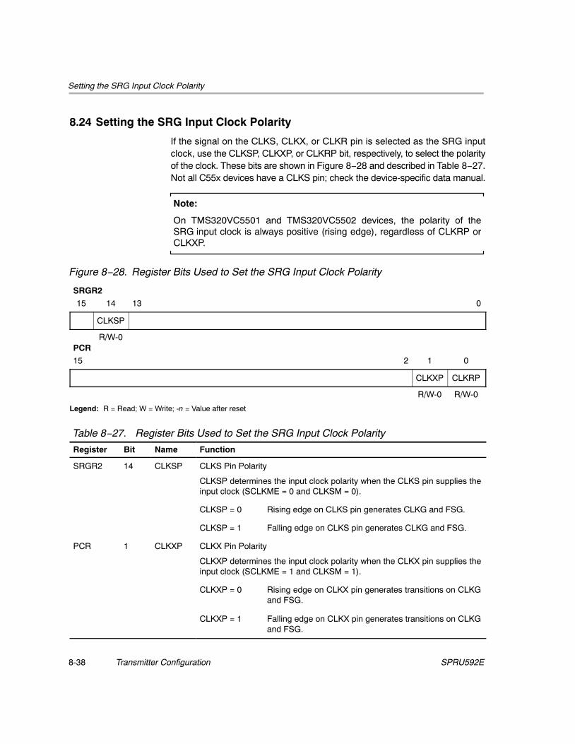
Setting the SRG Input Clock Polarity
Transmitter Configuration8-38 SPRU592E
8.24 Setting the SRG Input Clock Polarity
If the signal on the CLKS, CLKX, or CLKR pin is selected as the SRG inputclock, use the CLKSP, CLKXP, or CLKRP bit, respectively, to select the polarityof the clock. These bits are shown in Figure 8−28 and described in Table 8−27.Not all C55x devices have a CLKS pin; check the device-specific data manual.
Note:
On TMS320VC5501 and TMS320VC5502 devices, the polarity of theSRG input clock is always positive (rising edge), regardless of CLKRP orCLKXP.
Figure 8−28. Register Bits Used to Set the SRG Input Clock Polarity
SRGR2
15 14 13 0
CLKSP
R/W-0PCR
15 2 1 0
CLKXP CLKRP
R/W-0 R/W-0
Legend: R = Read; W = Write; -n = Value after reset
Table 8−27. Register Bits Used to Set the SRG Input Clock Polarity
Register Bit Name Function
SRGR2 14 CLKSP CLKS Pin Polarity
CLKSP determines the input clock polarity when the CLKS pin supplies theinput clock (SCLKME = 0 and CLKSM = 0).
CLKSP = 0 Rising edge on CLKS pin generates CLKG and FSG.
CLKSP = 1 Falling edge on CLKS pin generates CLKG and FSG.
PCR 1 CLKXP CLKX Pin Polarity
CLKXP determines the input clock polarity when the CLKX pin supplies theinput clock (SCLKME = 1 and CLKSM = 1).
CLKXP = 0 Rising edge on CLKX pin generates transitions on CLKGand FSG.
CLKXP = 1 Falling edge on CLKX pin generates transitions on CLKGand FSG.

Setting the SRG Input Clock Polarity
8-39Transmitter ConfigurationSPRU592E
Table 8−27. Register Bits Used to Set the SRG Input Clock Polarity (Continued)
Register FunctionNameBit
PCR 0 CLKRP CLKR Pin Polarity
CLKRP determines the input clock polarity when the CLKR pin supplies theinput clock (SCLKME = 1 and CLKSM = 0).
CLKRP = 0 Rising edge on CLKR pin generates transitions on CLKGand FSG.
CLKRP = 1 Falling edge on CLKR pin generates transitions on CLKGand FSG.
8.24.1 Using CLKSP/CLKXP/CLKRP to Choose an Input Clock Polarity
The sample rate generator can produce a clock signal (CLKG) and aframe-sync signal (FSG) for use by the receiver, the transmitter, or both. Toproduce CLKG and FSG, the sample rate generator must be driven by an inputclock signal derived from the McBSP internal input clock or from an externalclock on the CLKX pin, CLKR pin, or (if present) CLKS pin. If you use a pin,choose a polarity for the SRG input clock by programming the appropriatepolarity bit (CLKXP for the CLKX pin, CLKRP for the CLKR pin, CLKSP for theCLKS pin). The polarity determines whether the rising or falling edge of theinput clock generates transitions on CLKG and FSG.
Note:
On TMS320VC5501 and TMS320VC5502 devices, the polarity of theSRG input clock is always positive (rising edge), regardless of CLKRP orCLKXP.

Transmitter Configuration8-40 SPRU592E
This page is intentionally left blank.

9-1
General-Purpose I/O on the McBSP Pins
This chapter summarizes how to use the McBSP pins as general-purpose I/O(GPIO) pins.
Topic Page
9.1 Using the McBSP Pins for GPIO 9-2. . . . . . . . . . . . . . . . . . . . . . . . . . . . . . . .
Chapter 9

Using the McBSP Pins for GPIO
General-Purpose I/O on the McBSP Pins9-2 SPRU592E
9.1 Using the McBSP Pins for GPIO
Table 9−1 summarizes how to use the McBSP pins as general-purpose I/O(GPIO) pins. All of the bits mentioned in the table except XRST and RRST arein the pin control register. XRST and RRST are in the serial port controlregisters.
To use receiver pins CLKR, FSR, and DR as general purpose I/O pins ratherthan as serial port pins, you must set two conditions:
� The receiver of the serial port is in reset (RRST = 0 in SPCR1).
� General-purpose I/O is enabled for the serial port receiver (RIOEN = 1 inPCR).
The CLKR and FSR pins can be individually configured as either input oroutput pins with the CLKRM and FSRM bits, respectively. The DR pin can onlybe an input pin. Table 9−1 shows which bits in PCR are used to read from/writeto these pins.
For the transmitter pins CLKX, FSX, and DX, you must meet two similarconditions:
� The transmitter of the serial port is in reset (XRST = 0 in SPCR2).
� General-purpose I/O is enabled for the serial port transmitter (XIOEN = 1in PCR).
The CLKX and FSX pins can be individually configured as input or output pinswith the CLKXM and FSXM bits, respectively. The DX pin can only be an outputpin. Table 9−1 shows which bits in PCR are used to read from/write to thesepins.
For the CLKS pin, all of the reset and I/O enable conditions must be met:
� Both the receiver and transmitter of the serial port are in reset (RRST = 0and XRST = 0).
� General-purpose I/O is enabled for both the receiver and the transmitter(RIOEN = 1 and XIOEN = 1).
The CLKS pin can only be an input pin. To read the status of the signal on theCLKS pin, read the CLKSSTAT bit in PCR. Not all C55x devices have aCLKS pin; check the device-specific data manual.
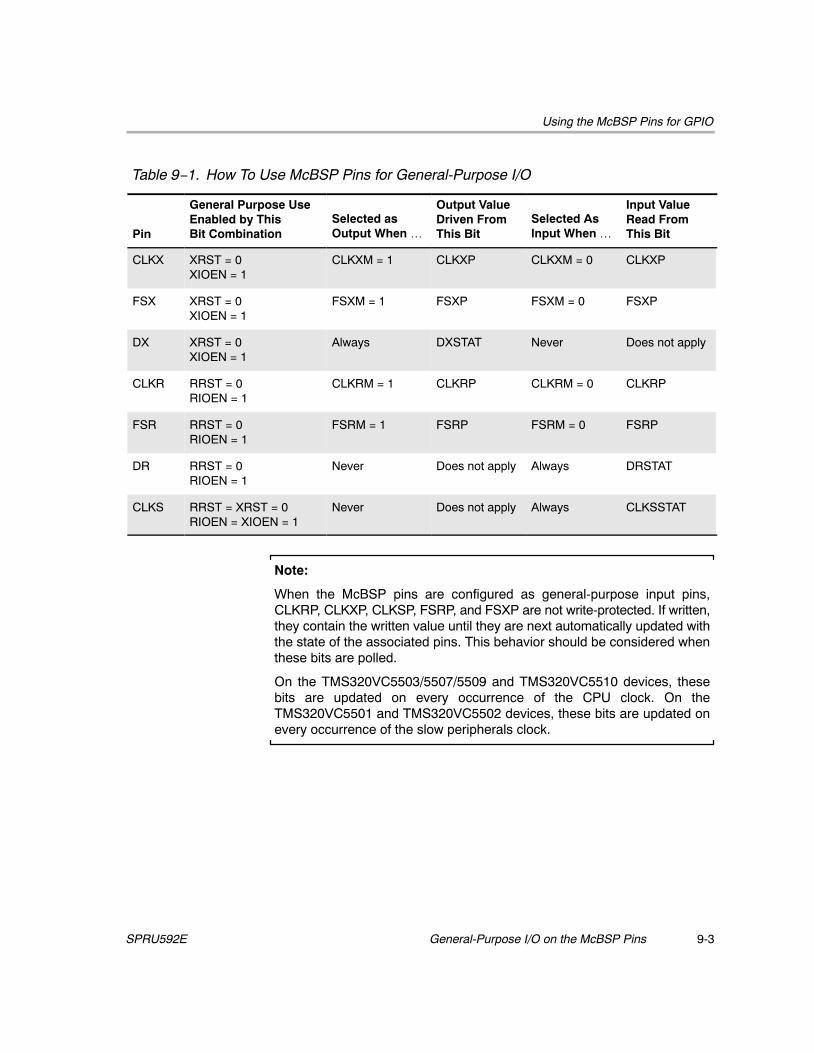
Using the McBSP Pins for GPIO
9-3General-Purpose I/O on the McBSP PinsSPRU592E
Table 9−1. How To Use McBSP Pins for General-Purpose I/O
Pin
General Purpose UseEnabled by ThisBit Combination
Selected as Output When …
Output Value Driven FromThis Bit
Selected AsInput When …
Input Value Read FromThis Bit
CLKX XRST = 0XIOEN = 1
CLKXM = 1 CLKXP CLKXM = 0 CLKXP
FSX XRST = 0XIOEN = 1
FSXM = 1 FSXP FSXM = 0 FSXP
DX XRST = 0XIOEN = 1
Always DXSTAT Never Does not apply
CLKR RRST = 0RIOEN = 1
CLKRM = 1 CLKRP CLKRM = 0 CLKRP
FSR RRST = 0RIOEN = 1
FSRM = 1 FSRP FSRM = 0 FSRP
DR RRST = 0RIOEN = 1
Never Does not apply Always DRSTAT
CLKS RRST = XRST = 0RIOEN = XIOEN = 1
Never Does not apply Always CLKSSTAT
Note:
When the McBSP pins are configured as general-purpose input pins,CLKRP, CLKXP, CLKSP, FSRP, and FSXP are not write-protected. If written,they contain the written value until they are next automatically updated withthe state of the associated pins. This behavior should be considered whenthese bits are polled.
On the TMS320VC5503/5507/5509 and TMS320VC5510 devices, thesebits are updated on every occurrence of the CPU clock. On theTMS320VC5501 and TMS320VC5502 devices, these bits are updated onevery occurrence of the slow peripherals clock.

General-Purpose I/O on the McBSP Pins9-4 SPRU592E
This page is intentionally left blank.

10-1
Emulation, Power, and Reset Considerations
This chapter covers the following topics:
� How to program the response of the McBSP to an emulation suspendevent (such as a breakpoint)
� How to conserve power in the DSP by placing the McBSP into its idle mode
� How to reset and initialize the various parts of the McBSP
Topic Page
10.1 McBSP Emulation Mode 10-2. . . . . . . . . . . . . . . . . . . . . . . . . . . . . . . . . . . . . .
10.2 McBSP Power Management on the TMS320VC5503/5507/5509 andTMS320VC5510 Devices 10-3. . . . . . . . . . . . . . . . . . . . . . . . . . . . . . . . . . . . . .
10.3 McBSP Power Management on the TMS320VC5501 andTMS320VC5502 Devices 10-4. . . . . . . . . . . . . . . . . . . . . . . . . . . . . . . . . . . . . .
10.4 Resetting and Initializing a McBSP 10-5. . . . . . . . . . . . . . . . . . . . . . . . . . . .
Chapter 10

McBSP Emulation Mode
Emulation, Power, and Reset Considerations10-2 SPRU592E
10.1 McBSP Emulation Mode
FREE and SOFT are special emulation bits in SPCR2 that determine the stateof the McBSP when an emulation suspend event occurs in the high-levellanguage debugger. An emulation suspend event corresponds to any type ofemulator access to the DSP, such as a hardware or software breakpoint, aprobepoint, or a printf instruction.
If FREE = 1 at the time of an emulation suspend event, the clock continues torun and data is still shifted out. When FREE = 1, the SOFT bit is a don’t care.
If FREE = 0, the SOFT bit takes effect: If SOFT = 0 when an emulationsuspend event occurs, the clock stops immediately, thus aborting atransmission. If SOFT = 1 and an emulation suspend event occurs whiletransmission is in progress, the transmission continues until completion of theword, and then the clock halts. These options are listed in Table 10−1.
The McBSP receiver responds to an emulation suspend event in a similarfashion. Note that if the receiver continues to run but the DMA controller isstopped, an overrun error is possible. In such a case, an interrupt serviceroutine should be in place to read the data receive registers (to restart theMcBSP receiver) or to reset the McBSP receiver.
Table 10−1. McBSP Emulation Modes Selectable With the FREE and SOFT Bitsof SPCR2
FREE SOFT McBSP Emulation Mode
0 0 Immediate stop mode (reset condition)
The transmitter and receiver stop immediately in response to anemulation suspend event.
0 1 Soft stop mode
When an emulation suspend event occurs, the transmitter stopsafter completion of the current word. The receiver is not affected.
1 0 or 1 Free run mode
The transmitter and receiver continue to run when an emulationsuspend event occurs.
Note:
On the TMS320VC5501 and TMS320VC5502 devices, there is an exceptionto the McBSP behavior when FREE = SOFT = 0: If the McBSP is in the SPImode, the transmitter stops immediately, but the receiver does not stop.

McBSP Power Management on the TMS320VC5503/5507/5509 and
10-3Emulation, Power, and Reset ConsiderationsSPRU592E
10.2 McBSP Power Management on the TMS320VC5503/5507/5509 andTMS320VC5510 Devices
The McBSP is placed into its idle mode with reduced power consumption whenthe PERIPH idle domain is idle (PERIS = 1 in ISTR) and the McBSP idleenable bit is set (IDLEEN = 1 in PCR).
In the McBSP idle mode:
� If the McBSP is configured to operate with internally generated clockingand frame synchronization, it will be completely stopped.
� If the McBSP is configured to operate with externally generated clockingand frame synchronization (either directly or through the sample rategenerator), the external interface portion of the McBSP continues tofunction during periods of external clock activity. The McBSP sends arequest to activate the PERIPH and DMA idle domains when it needs tobe serviced. If the domains were idle, they are made idle again after theMcBSP has been serviced.
When IDLEEN = 0 in PCR, the McBSP keeps running, regardless of whetherthe PERIPH domain is idle.
McBSP Power Management on the TMS320VC5503/5507/5509 and TMS320VC5510 Devices

McBSP Power Management on the TMS320VC5501 and
Emulation, Power, and Reset Considerations10-4 SPRU592E
10.3 McBSP Power Management on the TMS320VC5501 andTMS320VC5502 Devices
The McBSP is placed into its idle mode with reduced power consumption whenthe PERIPH idle domain is idle (PERIS = 1 in ISTR) and the McBSP idleenable bit is set (SPn = 1) in the peripheral idle control register (PICR).
Note:
If the McBSP is configured to use the internal Slow Peripherals clock(SYSCLK2) for any clocking or frame synchronization, the McBSP cannot beidled unless its transmitter and receiver are in their reset states (RRST = 0in SPCR1 and XRST = 0 in SPCR2).
In the McBSP idle mode:
� If the McBSP is configured to operate with internally generated clockingand frame synchronization, it will be completely stopped.
� If the McBSP is configured to operate with externally generated clockingand frame synchronization (either directly or through the sample rategenerator), the external interface portion of the McBSP continues tofunction during periods of external clock activity. The McBSP sends arequest to activate the PERIPH and DMA idle domains when it needs tobe serviced. If the domains were idle, they are made idle again after theMcBSP has been serviced.
When SPn= 0 in PICR, the McBSP keeps running, regardless of whether thePERIPH domain is idle.
McBSP Power Management on the TMS320VC5501 and TMS320VC5502 Devices
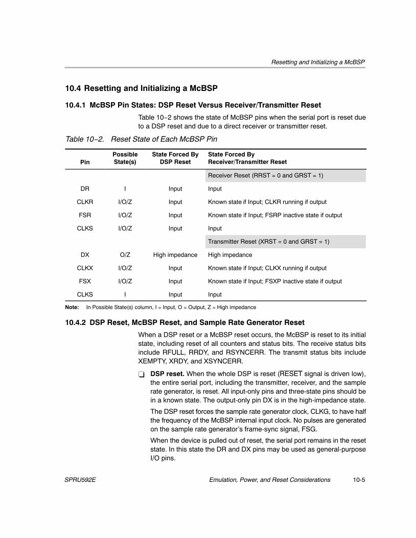
Resetting and Initializing a McBSP
10-5Emulation, Power, and Reset ConsiderationsSPRU592E
10.4 Resetting and Initializing a McBSP
10.4.1 McBSP Pin States: DSP Reset Versus Receiver/Transmitter Reset
Table 10−2 shows the state of McBSP pins when the serial port is reset dueto a DSP reset and due to a direct receiver or transmitter reset.
Table 10−2. Reset State of Each McBSP Pin
PinPossibleState(s)
State Forced ByDSP Reset
State Forced ByReceiver/Transmitter Reset
Receiver Reset (RRST = 0 and GRST = 1)
DR I Input Input
CLKR I/O/Z Input Known state if Input; CLKR running if output
FSR I/O/Z Input Known state if Input; FSRP inactive state if output
CLKS I/O/Z Input Input
Transmitter Reset (XRST = 0 and GRST = 1)
DX O/Z High impedance High impedance
CLKX I/O/Z Input Known state if Input; CLKX running if output
FSX I/O/Z Input Known state if Input; FSXP inactive state if output
CLKS I Input Input
Note: In Possible State(s) column, I = Input, O = Output, Z = High impedance
10.4.2 DSP Reset, McBSP Reset, and Sample Rate Generator Reset
When a DSP reset or a McBSP reset occurs, the McBSP is reset to its initialstate, including reset of all counters and status bits. The receive status bitsinclude RFULL, RRDY, and RSYNCERR. The transmit status bits includeXEMPTY, XRDY, and XSYNCERR.
� DSP reset. When the whole DSP is reset (RESET signal is driven low),the entire serial port, including the transmitter, receiver, and the samplerate generator, is reset. All input-only pins and three-state pins should bein a known state. The output-only pin DX is in the high-impedance state.
The DSP reset forces the sample rate generator clock, CLKG, to have halfthe frequency of the McBSP internal input clock. No pulses are generatedon the sample rate generator’s frame-sync signal, FSG.
When the device is pulled out of reset, the serial port remains in the resetstate. In this state the DR and DX pins may be used as general-purposeI/O pins.

Resetting and Initializing a McBSP
Emulation, Power, and Reset Considerations10-6 SPRU592E
� McBSP reset. When the receiver and transmitter reset bits, RRST andXRST, are loaded with 0s, the respective portions of the McBSP are reset,and activity in the corresponding section of the serial port stops. Allinput-only pins, such as DR and CLKS, and all other pins that areconfigured as inputs, are in a known state. The FSR and FSX pins aredriven to their inactive state if they are not outputs. If the CLKR and CLKXpins are programmed as outputs, they will be driven by CLKG, providedthat GRST = 1. Lastly, the DX pin will be in the high-impedance state whenthe transmitter and/or the device is reset.
During normal operation, the sample rate generator is reset if the GRST bitis cleared. GRST should be 0 only when neither the transmitter nor thereceiver is using the sample rate generator. In this case, the internalsample rate generator clock (CLKG) and its frame-sync signal (FSG) aredriven inactive low.
When the sample rate generator is not in the reset state (GRST = 1), pinsFSR and FSX are in an inactive state when RRST = 0 and XRST = 0,respectively, even if they are outputs driven by FSG. This ensures thatwhen only one portion of the McBSP is in reset, the other portion cancontinue operation when FRST = 1 and its frame synchronization is drivenby FSG.
� Sample rate generator reset. The sample rate generator is reset whenthe DSP is reset or when GRST is loaded with 0. In the case of a DSP reset,the sample rate generator clock, CLKG, is driven by the McBSP internalinput clock divided by 2, and the frame-sync signal, FSG, is driven inactivelow.
When neither the transmitter nor the receiver is fed by CLKG and FSG,you can reset the sample rate generator by clearing GRST. In this case,CLKG and FSG are driven inactive low. If you then set GRST, CLKG startsand runs as programmed. Later, if FRST = 1, FSG pulses active high afterthe programmed number of CLKG cycles has elapsed.
10.4.3 McBSP Initialization Procedure
The serial port initialization procedure is as follows:
1) Make XRST = RRST = FRST = GRST = 0 in SPCR[1,2]. If coming out ofa DSP reset, this step is not required.
2) While the serial port is in the reset state, program only the McBSPconfiguration registers (not the data registers) as required.
3) Wait for two clock cycles. This ensures proper internal synchronization.

Resetting and Initializing a McBSP
10-7Emulation, Power, and Reset ConsiderationsSPRU592E
4) Set GRST = 1 to enable the sample rate generator.
5) Wait for two clock cycles. This ensures proper internal synchronization.
6) Set up data acquisition as required (such as writing to DXR[1,2]).
7) Make XRST = RRST = 1 to enable the serial port. Make sure that as youset these reset bits, you do not modify any of the other bits in SPCR1 andSPCR2. Otherwise, you will change the configuration you selected instep 2.
8) Set FRST = 1, if internally generated frame synchronization is required.
9) Wait two clock cycles for the receiver and transmitter to become active.
Alternatively, on either write (step 1 or 5), the transmitter and receiver can beplaced in or taken out of reset individually by a modification of the desired bit.
The above procedure for reset/initialization can be applied in general when thereceiver or transmitter has to be reset during its normal operation, and alsowhen the sample rate generator is not used for either operation.
Notes:
1) The necessary duration of the active-low period of XRST or RRST is atleast two CLKR/CLKX cycles.
2) The appropriate bits in serial port configuration registers SPCR[1,2],PCR, RCR[1,2], XCR[1,2], and SRGR[1,2] should only be modifiedwhen the affected portion of the serial port is in its reset state.
3) In most cases, the data transmit registers (DXR[1,2]) should be loadedby the CPU or by the DMA controller only when the transmitter is enabled(XRST = 1). An exception to this rule is when these registers are usedfor companding internal data.
4) The bits of the channel control registers, MCR[1,2], RCER[A–H], andXCER[A–H], can be modified at any time as long as they are not beingused by the current reception/transmission in a multichannel selectionmode.

Resetting and Initializing a McBSP
Emulation, Power, and Reset Considerations10-8 SPRU592E
10.4.4 Resetting the Transmitter While the Receiver is Running
Example 10−1 shows one case in which the transmitter is reset and configuredwhile the receiver is running.
Example 10−1. Resetting and Configuring the McBSP Transmitter While theMcBSP Receiver Running
SPCR1 = 0001hSPCR2 = 0030h
; The receiver is running with the receive; interrupt (RINT) triggered by the; receiver ready bit (RRDY). The; transmitter is in its reset state. The; transmit interrupt (XINT) will be; triggered by the transmit frame−sync; error bit (XSYNCERR).
PCR = 0900h ; Transmit frame synchronization is; generated internally according to the; FSGM bit of SRGR2. The transmit clock; is driven by an external source. Receive; frame synchronization continues to be; driven by an external source. The; receive clock continues to be driven by; the sample rate generator. The input; clock of the sample rate generator is; supplied by the CLKS pin or by the; McBSP internal input clock, depending on; the CLKSM bit of SRGR2.
SRGR1 = 0001hSRGR2 = 2000h
; The McBSP internal input clock is the; input clock for the sample rate; generator. The sample rate generator; divides the McBSP internal input clock; by 2 to generate its output clock; (CLKG). Transmit frame synchronization; is tied to the automatic copying of data; from the DXR(s) to the XSR(s).
XCR1 = 0740hXCR2 = 8321h
; The transmit frame has two phases.; Phase 1 has eight 16−bit words. Phase 2; has four 12−bit words. There is a 1−bit; data delay between the start of a; frame−sync pulse and the first data bit; transmitted.
SPCR2 = 0031h ; The transmitter is taken out of reset.

Resetting and Initializing a McBSP
10-9Emulation, Power, and Reset ConsiderationsSPRU592E
Note:
The frame-sync pulse can be generated internally by the sample rate gener-ator or it can be supplied externally by another source. In a multichannelmode configuration with external frame-sync generation, theTMS320VC5501/02 McBSP transmitter will ignore the first frame-sync pulseafter it is taken out of reset. The transmitter will transmit only on the secondframe-sync pulse. The receiver will shift in data on the first frame-sync pulseregardless of whether it is generated internally or externally.

Emulation, Power, and Reset Considerations10-10 SPRU592E
11-1
Data Packing Examples
This chapter shows two ways you can implement data packing with theMcBSP.
Topic Page
11.1 Data Packing Using Frame Length and Word Length 11-2. . . . . . . . . . . .
11.2 Data Packing Using Word Length and the Frame-SyncIgnore Function 11-4. . . . . . . . . . . . . . . . . . . . . . . . . . . . . . . . . . . . . . . . . . . . . .
Chapter 11

Data Packing Using Frame Length and Word Length
Data Packing Examples11-2 SPRU592E
11.1 Data Packing Using Frame Length and Word Length
The frame length and word length can be manipulated to effectively pack data.For example, consider a situation where four 8-bit words are transferred in asingle-phase frame as shown in Figure 11−1. In this case:
� (R/X)PHASE = 0: Single-phase frame
� (R/X)FRLEN1 = 0000011b: 4-word frame
� (R/X)WDLEN1 = 000b: 8-bit words
Four 8-bit data words are transferred to and from the McBSP by the CPU orby the DMA controller. Thus, four reads from DRR1 and four writes to DXR1are necessary for each frame.
Figure 11−1.Four 8-Bit Data Words Transferred To/From the McBSP
RSR1 toRBR1 copy RBR1 copy
RSR1 to RSR1 toRBR1 copy RBR1 copy
RSR1 to
DXR1 to XSR1copy
DXR1 to XSR1copy
DXR1 to XSR1copy
DXR1 to XSR1copy
Word 1 Word 2 Word 3 Word 4
CLKR
FSR
DR
CLKX
FSX
DX
This data can also be treated as a single-phase frame consisting of one 32-bitdata word, as shown in Figure 11−2. In this case:
� (R/X)PHASE = 0: Single-phase frame
� (R/X)FRLEN1 = 0000000b: 1-word frame
� (R/X)WDLEN1 = 101b: 32-bit word

Data Packing Using Frame Length and Word Length
11-3Data Packing ExamplesSPRU592E
Two 16-bit data words are transferred to and from the McBSP by the CPU orby the DMA controller. Therefore, two reads, from DRR2 and DRR1, and twowrites, to DXR2 and DXR1, are necessary for each frame. This results in onlyhalf the number of transfers compared to the previous case. This manipulationreduces the percentage of bus time required for serial port data movement.
Note:
When the word length is larger than 16 bits, make sure you accessDRR2/DXR2 before you access DRR1/DXR1. McBSP activity is tied toaccesses of DRR1/DXR1. During the reception of 24-bit or 32-bit words,read DRR2 and then read DRR1. Otherwise, the next RBR[1,2]-to-DRR[1,2]copy occurs before DRR2 is read. Similarly, during the transmission of 24-bitor 32-bit words, write to DXR2 and then write to DXR1. Otherwise, the nextDXR[1,2]-to-XSR[1,2] copy occurs before DXR2 is loaded with new data.
Figure 11−2.One 32-Bit Data Word Transferred To/From the McBSP
DRR2 copyRBR2 to
DRR1 copyRBR1 to
DXR0 to XSR0copy
DXR1 to XSR1copy
Word 1
CLKR
FSR
DR
CLKX
FSX
DX
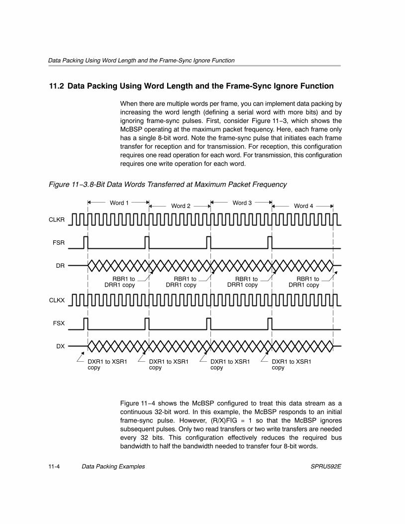
Data Packing Using Word Length and the Frame-Sync Ignore Function
Data Packing Examples11-4 SPRU592E
11.2 Data Packing Using Word Length and the Frame-Sync Ignore Function
When there are multiple words per frame, you can implement data packing byincreasing the word length (defining a serial word with more bits) and byignoring frame-sync pulses. First, consider Figure 11−3, which shows theMcBSP operating at the maximum packet frequency. Here, each frame onlyhas a single 8-bit word. Note the frame-sync pulse that initiates each frametransfer for reception and for transmission. For reception, this configurationrequires one read operation for each word. For transmission, this configurationrequires one write operation for each word.
Figure 11−3.8-Bit Data Words Transferred at Maximum Packet Frequency
RBR1 toDRR1 copy DRR1 copy
RBR1 to RBR1 toDRR1 copy DRR1 copy
RBR1 to
DXR1 to XSR1copy
DXR1 to XSR1copy
DXR1 to XSR1copy
DXR1 to XSR1copy
Word 1 Word 2 Word 3 Word 4
CLKR
FSR
DR
CLKX
FSX
DX
Figure 11−4 shows the McBSP configured to treat this data stream as acontinuous 32-bit word. In this example, the McBSP responds to an initialframe-sync pulse. However, (R/X)FIG = 1 so that the McBSP ignoressubsequent pulses. Only two read transfers or two write transfers are neededevery 32 bits. This configuration effectively reduces the required busbandwidth to half the bandwidth needed to transfer four 8-bit words.

Data Packing Using Word Length and the Frame-Sync Ignore Function
11-5Data Packing ExamplesSPRU592E
Figure 11−4.Configuring the Data Stream of Figure 11−3 as a Continuous 32-Bit Word
DRR1 copyRBR1 to
DRR1 copyRBR1 to
DXR2 to XSR2 copy DXR1 to XSR1 copy
Word 1
CLKR
FSR
DR
CLKX
FSX
DX
Frame ignored Frame ignored Frame ignored
Frame ignored Frame ignored Frame ignored
Note:
On the TMS320VC5501 and TMS320VC5502 devices, if a 0-bit delay andan external clock are used, the transfer shown in Figure 11−3 can only beachieved if the frame-sync ignore bit is set to 1. If the frame-sync ignore bitis 0, an additional clock cycle is required between frames.

Data Packing Examples11-6 SPRU592E
This page is intentionally left blank.
12-1
McBSP Registers
The McBSP registers are described in this chapter. For the I/O address of eachregister in a particular C55x device, see the device-specific data manual.
Topic Page
12.1 Data Receive Registers (DRR1 and DRR2) 12-2. . . . . . . . . . . . . . . . . . . . .
12.2 Data Transmit Registers (DXR1 and DXR2) 12-3. . . . . . . . . . . . . . . . . . . .
12.3 Serial Port Control Registers (SPCR1 and SPCR2) 12-4. . . . . . . . . . . . .
12.4 Receive Control Registers (RCR1 and RCR2) 12-13. . . . . . . . . . . . . . . . .
12.5 Transmit Control Registers (XCR1 and XCR2) 12-19. . . . . . . . . . . . . . . . .
12.6 Sample Rate Generator Registers (SRGR1 and SRGR2) 12-25. . . . . . .
12.7 Multichannel Control Registers (MCR1 and MCR2) 12-31. . . . . . . . . . . .
12.8 Pin Control Register (PCR) 12-38. . . . . . . . . . . . . . . . . . . . . . . . . . . . . . . . . .
12.9 Receive Channel Enable Registers (RCERA-RCERH) 12-46. . . . . . . . . .
12.10 Transmit Channel Enable Registers (XCERA-XCERH) 12-49. . . . . . . . .
Chapter 12

Data Receive Registers (DRR1 and DRR2)
McBSP Registers12-2 SPRU592E
12.1 Data Receive Registers (DRR1 and DRR2)
The CPU or the DMA controller reads received data from one or both of thedata receive registers (see Figure 12−1). If the serial word length is 16 bits orsmaller only DRR1 is used. If the serial length is larger than 16 bits, both DRR1and DRR2 are used, and DRR2 holds the most significant bits. Each frame ofreceive data in the McBSP can have one phase or two phases, each with itsown serial word length.
DRR1 and DRR2 are I/O mapped registers; they are accessible at addressesin I/O space.
Figure 12−1. Data Receive Registers (DRR1 and DRR2)
DRR2
15 0
High part of receive data (for 20-, 24- or 32-bit data)
R/W-0DRR1
15 0
Receive data (for 8-, 12-, or 16-bit data) or Low part of receive data (for 20-, 24- or 32-bit data)
R/W-0
Legend: R = Read; W = Write; -n = Value after reset
12.1.1 How Data Travels From the Data Receive (DR) Pin to the DRRs
If the serial word length is 16 bits or smaller, receive data on the DR pin isshifted into receive shift register 1 (RSR1) and then copied into receive bufferregister 1 (RBR1). The content of RBR1 is then copied to DRR1, which can beread by the CPU or by the DMA controller.
If the serial word length is larger than 16 bits, receive data on the DR pin isshifted into both of the receive shift registers (RSR2, RSR1) and then copiedinto both of the receive buffer registers (RBR2, RBR1). The content of theRBRs is then copied into both of the DRRs, which can be read by the CPU orby the DMA controller.
If companding is used during the copy from RBR1 to DRR1(RCOMPAND = 10b or 11b), the 8-bit compressed data in RBR1 is expandedto a left-justified 16-bit value in DRR1. If companding is disabled, the datacopied from RBR[1,2] to DRR[1,2] is justified and bit filled according to theRJUST bits.
The RSRs and RBRs are not accessible. They are not mapped to I/O spacelike the DRRs.
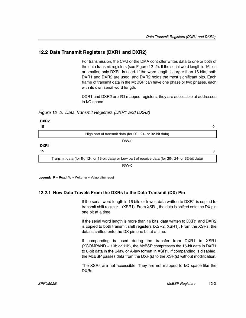
Data Transmit Registers (DXR1 and DXR2)
12-3McBSP RegistersSPRU592E
12.2 Data Transmit Registers (DXR1 and DXR2)
For transmission, the CPU or the DMA controller writes data to one or both ofthe data transmit registers (see Figure 12−2). If the serial word length is 16 bitsor smaller, only DXR1 is used. If the word length is larger than 16 bits, bothDXR1 and DXR2 are used, and DXR2 holds the most significant bits. Eachframe of transmit data in the McBSP can have one phase or two phases, eachwith its own serial word length.
DXR1 and DXR2 are I/O mapped registers; they are accessible at addressesin I/O space.
Figure 12−2. Data Transmit Registers (DXR1 and DXR2)
DXR2
15 0
High part of transmit data (for 20-, 24- or 32-bit data)
R/W-0DXR1
15 0
Transmit data (for 8-, 12-, or 16-bit data) or Low part of receive data (for 20-, 24- or 32-bit data)
R/W-0
Legend: R = Read; W = Write; -n = Value after reset
12.2.1 How Data Travels From the DXRs to the Data Transmit (DX) Pin
If the serial word length is 16 bits or fewer, data written to DXR1 is copied totransmit shift register 1 (XSR1). From XSR1, the data is shifted onto the DX pinone bit at a time.
If the serial word length is more than 16 bits, data written to DXR1 and DXR2is copied to both transmit shift registers (XSR2, XSR1). From the XSRs, thedata is shifted onto the DX pin one bit at a time.
If companding is used during the transfer from DXR1 to XSR1(XCOMPAND = 10b or 11b), the McBSP compresses the 16-bit data in DXR1to 8-bit data in the µ-law or A-law format in XSR1. If companding is disabled,the McBSP passes data from the DXR(s) to the XSR(s) without modification.
The XSRs are not accessible. They are not mapped to I/O space like theDXRs.

Serial Port Control Registers (SPCR1 and SPCR2)
McBSP Registers12-4 SPRU592E
12.3 Serial Port Control Registers (SPCR1 and SPCR2)
Each McBSP has two serial port control registers of the form shown inFigure 12−3. Table 12−1 and Table 12−2 describe the bits in SPCR1 andSPCR2, respectively. These I/O-mapped registers enable you to:
� Control various McBSP modes: digital loopback mode (DLB),sign-extension and justification mode for reception (RJUST), clock stopmode (CLKSTP), interrupt modes (RINTM and XINTM), emulation mode(FREE and SOFT)
� Turn on and off the DX-pin delay enabler (DXENA)
� Check the status of receive and transmit operations (RSYNCERR,XSYNCERR, RFULL, XEMPTY, RRDY, XRDY)
� Reset portions of the McBSP (RRST, XRST, FRST, GRST)
Figure 12−3. Serial Port Control Registers (SPCR1 and SPCR2)
SPCR1
15 14 13 12 11 10 8
DLB RJUST CLKSTP Reserved
R/W-0 R/W-00 R/W-00 R-0
7 6 5 4 3 2 1 0
DXENA Reserved† RINTM RSYNCERR RFULL RRDY RRST
R/W-0 R/W-0 R/W-00 R/W-0 R-0 R-0 R/W-0
SPCR2
15 10 9 8
Reserved FREE SOFT
R-0 R/W-0 R/W-0
7 6 5 4 3 2 1 0
FRST GRST XINTM XSYNCERR XEMPTY XRDY XRST
R/W-0 R/W-0 R/W-00 R/W-0 R-0 R-0 R/W-0
Legend: R = Read; W = Write; -n = Value after reset† Always write 0 to this reserved bit.

Serial Port Control Registers (SPCR1 and SPCR2)
12-5McBSP RegistersSPRU592E
Table 12−1. SPCR1 Bit Descriptions
Bit Field Value Description
15 DLB Digital loopback mode bit. DLB disables or enables the digital loopbackmode of the McBSP:
0 Disabled
Internal DR is supplied by the DR pin. Internal FSR and internal CLKR canbe supplied by their respective pins or by the sample rate generator,depending on the mode bits FSRM and CLKRM.
1 Enabled
Internal receive signals are supplied by internal transmit signals:DR connected to DXFSR connected to FSXCLKR connected to CLKX
Internal DX is supplied by the DX pin. Internal FSX and internal CLKX aresupplied by their respective pins or are generated internally, depending onthe mode bits FSXM and CLKXM.
This mode allows you to test serial port code with a single DSP. The McBSPtransmitter directly supplies data, frame synchronization, and clocking tothe McBSP receiver.
14–13 RJUST Receive sign-extension and justification mode bits. During reception,RJUST determines how data is justified and bit filled before being passedto the data receive registers (DRR1, DRR2).
Note: RJUST is ignored if you enable a companding mode with theRCOMPAND bits. In a companding mode, the 8-bit compressed data inRBR1 is expanded to left-justified 16-bit data in DRR1.
00b Right justify the data and zero fill the MSBs.
01b Right justify the data and sign-extend the data into the MSBs.
10b Left justify the data and zero fill the LSBs.
11b Reserved (do not use)

Serial Port Control Registers (SPCR1 and SPCR2)
McBSP Registers12-6 SPRU592E
Table 12−1. SPCR1 Bit Descriptions (Continued)
Bit DescriptionValueField
12–11 CLKSTP Clock stop mode bits. CLKSTP allows you to use the clock stop mode tosupport the SPI master-slave protocol. If you will not be using the SPIprotocol, you can clear CLKSTP to disable the clock stop mode.
In the clock stop mode, the clock stops at the end of each data transfer. Atthe beginning of each data transfer, the clock starts immediately(CLKSTP = 10b) or after a half-cycle delay (CLKSTP = 11b).
00b or01b
Clock stop mode is disabled.
10b Clock stop mode, without clock delay
11b Clock stop mode, with half-cycle clock delay
10-8 Reserved These read-only reserved bits return 0s when read.
7 DXENA DX delay enabler mode bit. DXENA controls the delay enabler for theDX pin. The enabler creates an extra delay for turn-on time (for the lengthof the delay for a particular C55x device, see the device-specific datamanual).
0 DX delay enabler off
1 DX delay enabler on
6 Reserved Always write 0 to this reserved bit.

Serial Port Control Registers (SPCR1 and SPCR2)
12-7McBSP RegistersSPRU592E
Table 12−1. SPCR1 Bit Descriptions (Continued)
Bit DescriptionValueField
5–4 RINTM Receive interrupt mode bits. RINTM determines which event in the McBSPreceiver generates a receive interrupt (RINT) request. If RINT is properlyenabled inside the CPU, the CPU services the interrupt request; otherwise,the CPU ignores the request.
00b The McBSP sends a receive interrupt (RINT) request to the CPU when theRRDY bit changes from 0 to 1, indicating that receive data is ready to beread (the content of RBR[1,2] has been copied to DRR[1,2]):
Note: Regardless of the value of RINTM, you can check RRDY to determinewhether a word transfer is complete.
01b In the multichannel selection mode, the McBSP sends a RINT request to theCPU after every 16-channel block is received in a frame.
Outside of the multichannel selection mode, no interrupt request is sent.
10b The McBSP sends a RINT request to the CPU when each receiveframe-sync pulse is detected. The interrupt request is sent even if thereceiver is in its reset state.
11b The McBSP sends a RINT request to the CPU when the RSYNCERR bitis set, indicating a receive frame-sync error.
Note: Regardless of the value of RINTM, you can check RSYNCERR todetermine whether a receive frame-sync error occurred.
3 RSYNCERR Receive frame-sync error bit. RSYNCERR is set when a receiveframe-sync error is detected by the McBSP. If RINTM = 11b, the McBSPsends a receive interrupt (RINT) request to the CPU when RSYNCERR isset. The flag remains set until you write a 0 to it or reset the receiver.
Caution: If RINTM = 11b, writing a 1 to RSYNCERR triggers a receiveinterrupt just as if a receive frame-sync error occurred.
0 No error
1 Receive frame-sync error
2 RFULL Receiver full bit. RFULL is set when the receiver is full with new data andthe previously received data has not been read (receiver-full condition).
0 No receiver-full condition
1 Receiver-full condition: RSR[1,2] and RBR[1,2] are full with new data, butthe previous data in DRR[1,2] has not been read.

Serial Port Control Registers (SPCR1 and SPCR2)
McBSP Registers12-8 SPRU592E
Table 12−1. SPCR1 Bit Descriptions (Continued)
Bit DescriptionValueField
1 RRDY Receiver ready bit. RRDY is set when data is ready to be read fromDRR[1,2]. Specifically, RRDY is set in response to a copy from RBR1 toDRR1.
If the receive interrupt mode is RINTM = 00b, the McBSP sends a receiveinterrupt request to the CPU when RRDY changes from 0 to 1.
Also, when RRDY changes from 0 to 1, the McBSP sends a receivesynchronization event (REVT) signal to the DMA controller.
0 Receiver not ready
When the content of DRR1 is read, RRDY is automatically cleared.
1 Receiver ready: New data can be read from DRR[1,2].
Important: If both DRRs are needed (word length larger than 16 bits), theCPU or the DMA controller must read from DRR2 first and then from DRR1.As soon as DRR1 is read, the next RBR-to-DRR copy is initiated. If DRR2is not read first, the data in DRR2 is lost.
0 RRST Receiver reset bit. You can use RRST to take the McBSP receiver into andout of its reset state. Note: This bit has a negative polarity; RRST = 0indicates the reset state.
0 If you read a 0, the receiver is in its reset state.
If you write a 0, you reset the receiver.
1 If you read a 1, the receiver is enabled.
If you write a 1, you enable the receiver by taking it out of its reset state.

Serial Port Control Registers (SPCR1 and SPCR2)
12-9McBSP RegistersSPRU592E
Table 12−2. SPCR2 Bit Descriptions
Bit Field Value Description
15-10 Reserved These read-only reserved bits return 0s when read.
9 FREE Free run bit. When an emulation suspend event (such as a breakpoint)occurs, FREE determines whether the McBSP transmit and receive clockscontinue to run or whether they are affected as determined by the SOFT bit.When one of the clocks stops, the corresponding data transfer(transmission or reception) stops.
0 The McBSP transmit and receive clocks are affected as determined by theSOFT bit.
1 Free run. The McBSP transmit and receive clocks continue to run.
8 SOFT Soft stop bit. When FREE = 0, SOFT determines the response of theMcBSP transmit and receive clocks when an emulation suspend event(such as a breakpoint) occurs. When one of the clocks stops, thecorresponding data transfer (transmission or reception) stops.
0 Hard stop. The McBSP transmit and receive clocks are stoppedimmediately.
1 Soft stop. The McBSP transmit clock stops after completion of the currentserial word transfer. The McBSP receive clock is not affected.
On the TMS320VC5501 and TMS320VC5502 devices, the SOFT operationworks as described above.
On the TMS320VC5510 and TMS320VC5503/5507/5509 devices, supportfor SOFT=1 is not available. If FREE = 0 and SOFT = 1, the serial port willcontinue to run on an emulation breakpoint.

Serial Port Control Registers (SPCR1 and SPCR2)
McBSP Registers12-10 SPRU592E
Table 12−2. SPCR2 Bit Descriptions (Continued)
Bit DescriptionValueField
7 FRST Frame-sync logic reset bit. The sample rate generator of the McBSPincludes frame-sync logic to generate an internal frame-sync signal. Youcan use FRST to take the frame-sync logic into and out of its reset state.Note: This bit has a negative polarity; FRST = 0 indicates the reset state.
0 If you read a 0, the frame-sync logic is in its reset state.
If you write a 0, you reset the frame-sync logic.
In the reset state, the frame-sync logic does not generate a frame-syncsignal (FSG).
1 If you read a 1, the frame-sync logic is enabled.
If you write a 1, you enable the frame-sync logic by taking it out of its resetstate.
When the frame-sync logic is enabled (FRST = 1) and the sample rategenerator as a whole is enabled (GRST = 1), the frame-sync logicgenerates the frame-sync signal FSG as programmed.
6 GRST Sample rate generator reset bit. You can use GRST to take the McBSPsample rate generator into and out of its reset state. Note: This bit has anegative polarity; GRST = 0 indicates the reset state.
0 If you read a 0, the sample rate generator is in its reset state.
If you write a 0, you reset the sample rate generator.
If GRST = 0 due to a DSP reset, CLKG is driven by the McBSP internal inputclock divided by 2, and FSG is driven low (inactive). If GRST = 0 due toprogram code, CLKG and FSG are both driven low (inactive).
1 If you read a 1, the sample rate generator is enabled.
If you write a 1, you enable the sample rate generator by taking it out of itsreset state.
When enabled, the sample rate generator generates the clock signal CLKGas programmed in the sample rate generator registers. If FRST = 1, thegenerator also generates the frame-sync signal FSG as programmed in thesample rate generator registers.

Serial Port Control Registers (SPCR1 and SPCR2)
12-11McBSP RegistersSPRU592E
Table 12−2. SPCR2 Bit Descriptions (Continued)
Bit DescriptionValueField
5–4 XINTM Transmit interrupt mode bits. XINTM determines which event in the McBSPtransmitter generates a transmit interrupt (XINT) request. If XINT is properlyenabled, the CPU services the interrupt request; otherwise, the CPUignores the request.
00b The McBSP sends a transmit interrupt (XINT) request to the CPU when theXRDY bit changes from 0 to 1, indicating that transmitter is ready to acceptnew data (the content of DXR[1,2] has been copied to XSR[1,2]):
Note: Regardless of the value of XINTM, you can check XRDY to determinewhether a word transfer is complete.
01b In the multichannel selection mode, the McBSP sends an XINT request tothe CPU after every 16-channel block is transmitted in a frame.
Outside of the multichannel selection mode, no interrupt request is sent.
10b The McBSP sends an XINT request to the CPU when each transmitframe-sync pulse is detected. The interrupt request is sent even if thetransmitter is in its reset state.
11b The McBSP sends an XINT request to the CPU when the XSYNCERR bitis set, indicating a transmit frame-sync error.
Note: Regardless of the value of XINTM, you can check XSYNCERR todetermine whether a transmit frame-sync error occurred.
3 XSYNCERR Transmit frame-sync error bit. XSYNCERR is set when a transmitframe-sync error is detected by the McBSP. If XINTM = 11b, the McBSPsends a transmit interrupt (XINT) request to the CPU when XSYNCERR isset. The flag remains set until you write a 0 to it or reset the transmitter.
Caution: if XINTM = 11b, writing a 1 to XSYNCERR triggers a transmitinterrupt just as if a transmit frame-sync error occurred.
0 No error
1 Transmit frame-sync error

Serial Port Control Registers (SPCR1 and SPCR2)
McBSP Registers12-12 SPRU592E
Table 12−2. SPCR2 Bit Descriptions (Continued)
Bit DescriptionValueField
2 XEMPTY Transmitter empty bit. XEMPTY is cleared when the transmitter is ready tosend new data but no new data is available (transmitter-empty condition).Note: This bit has a negative polarity; a transmitter-empty condition isindicated by XEMPTY = 0.
0 Transmitter-empty condition
Typically this indicates that all the bits of the current word have beentransmitted but there is no new data in DXR1. XEMPTY is also cleared if thetransmitter is reset and then restarted.
1 No transmitter-empty condition
1 XRDY Transmitter ready bit. XRDY is set when the transmitter is ready to acceptnew data in DXR[1,2]. Specifically, XRDY is set in response to a copy fromDXR1 to XSR1.
If the transmit interrupt mode is XINTM = 00b, the McBSP sends a transmitinterrupt (XINT) request to the CPU when XRDY changes from 0 to 1.
Also, when XRDY changes from 0 to 1, the McBSP sends a transmitsynchronization event (XEVT) signal to the DMA controller.
0 Transmitter not ready
When DXR1 is loaded, XRDY is automatically cleared.
1 Transmitter ready: DXR[1,2] is ready to accept new data.
Important: If both DXRs are needed (word length larger than 16 bits), theCPU or the DMA controller must load DXR2 first and then load DXR1. Assoon as DXR1 is loaded, the contents of both DXRs are copied to thetransmit shift registers (XSRs), as described in the next step. If DXR2 is notloaded first, the previous content of DXR2 is passed to the XSR2.
0 XRST Transmitter reset bit. You can use XRST to take the McBSP transmitter intoand out of its reset state. Note: This bit has a negative polarity; XRST = 0indicates the reset state.
0 If you read a 0, the transmitter is in its reset state.
If you write a 0, you reset the transmitter.
1 If you read a 1, the transmitter is enabled.
If you write a 1, you enable the transmitter by taking it out of its reset state.

Receive Control Registers (RCR1 and RCR2)
12-13McBSP RegistersSPRU592E
12.4 Receive Control Registers (RCR1 and RCR2)
Each McBSP has two receive control registers of the form shown inFigure 12−4. Table 12−3 and Table 12−4 describe the bits of RCR1 andRCR2, respectively. These I/O-mapped registers enable you to:
� Specify one or two phases for each frame of receive data (RPHASE)
� Define two parameters for phase 1 and (if necessary) phase 2: the serialword length (RWDLEN1, RWDLEN2) and the number of words(RFRLEN1, RFRLEN2)
� Choose a receive companding mode, if any (RCOMPAND)
� Enable or disable the receive frame-sync ignore function (RFIG)
� Choose a receive data delay (RDATDLY)
Figure 12−4. Receive Control Registers (RCR1 and RCR2)
RCR1
15 14 8
Reserved RFRLEN1
R-0 R/W-0
7 5 4 0
RWDLEN1 Reserved
R/W-000 R-0
RCR2
15 14 8
RPHASE RFRLEN2
R/W-0 R/W-0
7 5 4 3 2 1 0
RWDLEN2 RCOMPAND RFIG RDATDLY
R/W-000 R/W-00 R/W-0 R/W-00
Legend: R = Read; W = Write; -n = Value after reset
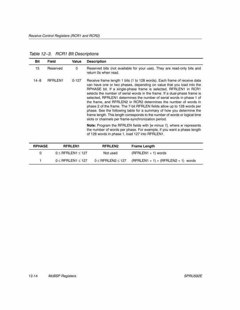
Receive Control Registers (RCR1 and RCR2)
McBSP Registers12-14 SPRU592E
Table 12−3. RCR1 BIt Descriptions
Bit Field Value Description
15 Reserved 0 Reserved bits (not available for your use). They are read-only bits andreturn 0s when read.
14–8 RFRLEN1 0-127 Receive frame length 1 bits (1 to 128 words). Each frame of receive datacan have one or two phases, depending on value that you load into theRPHASE bit. If a single-phase frame is selected, RFRLEN1 in RCR1selects the number of serial words in the frame. If a dual-phase frame isselected, RFRLEN1 determines the number of serial words in phase 1 ofthe frame, and RFRLEN2 in RCR2 determines the number of words inphase 2 of the frame. The 7-bit RFRLEN fields allow up to 128 words perphase. See the following table for a summary of how you determine theframe length. This length corresponds to the number of words or logical timeslots or channels per frame-synchronization period.
Note: Program the RFRLEN fields with [w minus 1], where w representsthe number of words per phase. For example, if you want a phase lengthof 128 words in phase 1, load 127 into RFRLEN1.
RPHASE RFRLEN1 RFRLEN2 Frame Length
0 0 ≤ RFRLEN1 ≤ 127 Not used (RFRLEN1 + 1) words
1 0 ≤ RFRLEN1 ≤ 127 0 ≤ RFRLEN2 ≤ 127 (RFRLEN1 + 1) + (RFRLEN2 + 1) words

Receive Control Registers (RCR1 and RCR2)
12-15McBSP RegistersSPRU592E
Table 12−3. RCR1 BIt Descriptions (Continued)
Bit Field Value Description
7–5 RWDLEN1 Receive word length 1 bits. Each frame of receive data can have one or twophases, depending on the value that you load into the RPHASE bit. If asingle-phase frame is selected, RWDLEN1 in RCR1 selects the length forevery serial word received in the frame. If a dual-phase frame is selected,RWDLEN1 determines the length of the serial words in phase 1 of the frame,and RWDLEN2 in RCR2 determines the word length in phase 2 of theframe.
000b 8 bits
001b 12 bits
010b 16 bits
011b 20 bits
100b 24 bits
101b 32 bits
other Reserved (do not use)
4-0 Reserved 0 Reserved bits (not available for your use). They are read-only bits andreturn 0s when read.

Receive Control Registers (RCR1 and RCR2)
McBSP Registers12-16 SPRU592E
Table 12−4. RCR2 Bit Descriptions
Bit Field Value Description
15 RPHASE Receive phase number bit. RPHASE determines whether the receive framehas one phase or two phases. For each phase you can define the serialword length and the number of serial words in the phase. To set up phase1, program RWDLEN1 (word length) and RFRLEN1 (number of words). Toset up phase 2 (if there are two phases), program RWDLEN2 andRFRLEN2.
0 Single-phase frame
The receive frame has only one phase, phase 1.
1 Dual-phase frame
The receive frame has two phases, phase 1 and phase 2.
14–8 RFRLEN2 0-127 Receive frame length 2 bits (1 to 128 words). Each frame of receive datacan have one or two phases, depending on value that you load into theRPHASE bit. If a single-phase frame is selected, RFRLEN1 in RCR1selects the number of serial words in the frame. If a dual-phase frame isselected, RFRLEN1 determines the number of serial words in phase 1 ofthe frame, and RFRLEN2 in RCR2 determines the number of words inphase 2 of the frame. The 7-bit RFRLEN fields allow up to 128 words perphase. See the following table for a summary of how to determine the framelength. This length corresponds to the number of words or logical time slotsor channels per frame-synchronization period.
Note: Program the RFRLEN fields with [w minus 1], where w represents thenumber of words per phase. For example, if you want a phase length of128 words in phase 2, load 127 into RFRLEN2.
RPHASE RFRLEN1 RFRLEN2 Frame Length
0 0 ≤ RFRLEN1 ≤ 127 Not used (RFRLEN1 + 1) words
1 0 ≤ RFRLEN1 ≤ 127 0 ≤ RFRLEN2 ≤ 127 (RFRLEN1 + 1) + (RFRLEN2 + 1) words

Receive Control Registers (RCR1 and RCR2)
12-17McBSP RegistersSPRU592E
Table 12−4. RCR2 BIt Descriptions (Continued)
Bit Field Value Description
7–5 RWDLEN2 Receive word length 2 bits. Each frame of receive data can have one ortwo phases, depending on the value that you load into the RPHASE bit.If a single-phase frame is selected, RWDLEN1 in RCR1 selects the lengthfor every serial word received in the frame. If a dual-phase frame isselected, RWDLEN1 determines the length of the serial words in phase1 of the frame, and RWDLEN2 in RCR2 determines the word length inphase 2 of the frame.
000b 8 bits
001b 12 bits
010b 16 bits
011b 20 bits
100b 24 bits
101b 32 bits
other Reserved (do not use)
4–3 RCOMPAND Receive companding mode bits. Companding (COMpress and exPAND)hardware allows compression and expansion of data in either µ-law orA-law format.
RCOMPAND allows you to choose one of the following compandingmodes for the McBSP receiver:
00b No companding, any size data, MSB received first
01b No companding, 8-bit data, LSB received first
10b µ-law companding, 8-bit data, MSB received first
11b A-law companding, 8-bit data, MSB received first
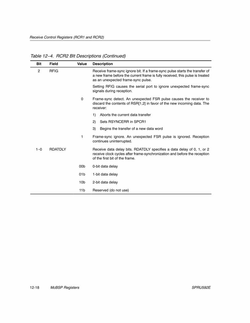
Receive Control Registers (RCR1 and RCR2)
McBSP Registers12-18 SPRU592E
Table 12−4. RCR2 BIt Descriptions (Continued)
Bit DescriptionValueField
2 RFIG Receive frame-sync ignore bit. If a frame-sync pulse starts the transfer ofa new frame before the current frame is fully received, this pulse is treatedas an unexpected frame-sync pulse.
Setting RFIG causes the serial port to ignore unexpected frame-syncsignals during reception.
0 Frame-sync detect. An unexpected FSR pulse causes the receiver todiscard the contents of RSR[1,2] in favor of the new incoming data. Thereceiver:
1) Aborts the current data transfer
2) Sets RSYNCERR in SPCR1
3) Begins the transfer of a new data word
1 Frame-sync ignore. An unexpected FSR pulse is ignored. Receptioncontinues uninterrupted.
1–0 RDATDLY Receive data delay bits. RDATDLY specifies a data delay of 0, 1, or 2receive clock cycles after frame-synchronization and before the receptionof the first bit of the frame.
00b 0-bit data delay
01b 1-bit data delay
10b 2-bit data delay
11b Reserved (do not use)
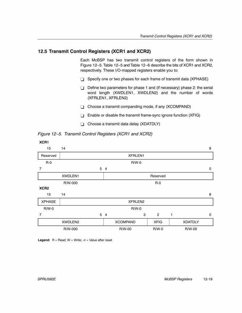
Transmit Control Registers (XCR1 and XCR2)
12-19McBSP RegistersSPRU592E
12.5 Transmit Control Registers (XCR1 and XCR2)
Each McBSP has two transmit control registers of the form shown inFigure 12−5. Table 12−5 and Table 12−6 describe the bits of XCR1 and XCR2,respectively. These I/O-mapped registers enable you to:
� Specify one or two phases for each frame of transmit data (XPHASE)
� Define two parameters for phase 1 and (if necessary) phase 2: the serialword length (XWDLEN1, XWDLEN2) and the number of words(XFRLEN1, XFRLEN2)
� Choose a transmit companding mode, if any (XCOMPAND)
� Enable or disable the transmit frame-sync ignore function (XFIG)
� Choose a transmit data delay (XDATDLY)
Figure 12−5. Transmit Control Registers (XCR1 and XCR2)
XCR1
15 14 8
Reserved XFRLEN1
R-0 R/W-0
7 5 4 0
XWDLEN1 Reserved
R/W-000 R-0
XCR2
15 14 8
XPHASE XFRLEN2
R/W-0 R/W-0
7 5 4 3 2 1 0
XWDLEN2 XCOMPAND XFIG XDATDLY
R/W-000 R/W-00 R/W-0 R/W-00
Legend: R = Read; W = Write; -n = Value after reset

Transmit Control Registers (XCR1 and XCR2)
McBSP Registers12-20 SPRU592E
Table 12−5. XCR1 Bit Descriptions
Bit Field Value Description
15 Reserved 0 Reserved bits (not available for your use). They are read-only bits andreturn 0s when read.
14–8 XFRLEN1 0-127 Transmit frame length 1 (1 to 128 words). Each frame of transmit data canhave one or two phases, depending on value that you load into the XPHASEbit. If a single-phase frame is selected, XFRLEN1 in XCR1 selects thenumber of serial words in the frame. If a dual-phase frame is selected,XFRLEN1 determines the number of serial words in phase 1 of the frame,and XFRLEN2 in XCR2 determines the number of words in phase 2 of theframe. The 7-bit XFRLEN fields allow up to 128 words per phase. See thefollowing table for a summary of how you determine the frame length. Thislength corresponds to the number of words or logical time slots or channelsper frame-synchronization period.
Note: Program the XFRLEN fields with [w minus 1], where w represents thenumber of words per phase. For example, if you want a phase length of128 words in phase 1, load 127 into XFRLEN1.
XPHASE XFRLEN1 XFRLEN2 Frame Length
0 0 ≤ XFRLEN1 ≤ 127 Not used (XFRLEN1 + 1) words
1 0 ≤ XFRLEN1 ≤ 127 0 ≤ XFRLEN2 ≤ 127 (XFRLEN1 + 1) + (XFRLEN2 + 1) words

Transmit Control Registers (XCR1 and XCR2)
12-21McBSP RegistersSPRU592E
Table 12−5. XCR1 Bit Descriptions (Continued)
Bit Field Value Description
7–5 XWDLEN1 Transmit word length 1. Each frame of transmit data can have one or twophases, depending on the value that you load into the XPHASE bit. If asingle-phase frame is selected, XWDLEN1 in XCR1 selects the length forevery serial word transmitted in the frame. If a dual-phase frame is selected,XWDLEN1 determines the length of the serial words in phase 1 of the frame,and XWDLEN2 in XCR2 determines the word length in phase 2 of the frame.
000b 8 bits
001b 12 bits
010b 16 bits
011b 20 bits
100b 24 bits
101b 32 bits
other Reserved (do not use)
4-0 Reserved 0 Reserved bits (not available for your use). They are read-only bits andreturn 0s when read.
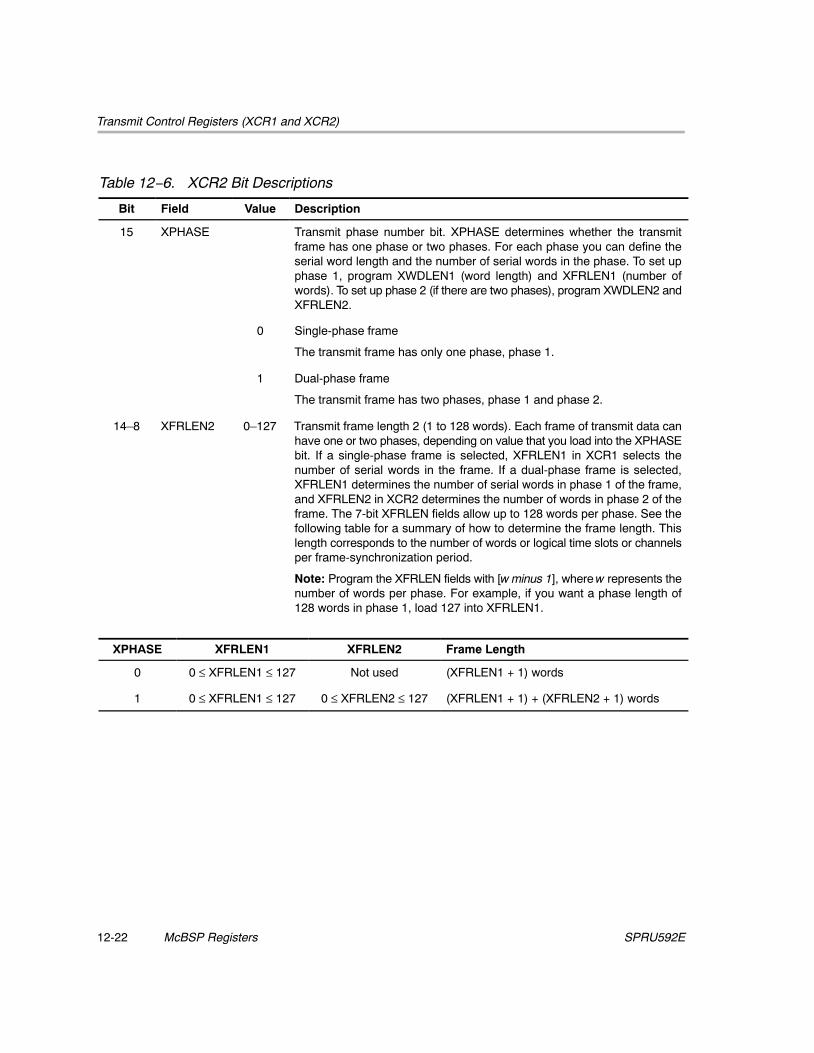
Transmit Control Registers (XCR1 and XCR2)
McBSP Registers12-22 SPRU592E
Table 12−6. XCR2 Bit Descriptions
Bit Field Value Description
15 XPHASE Transmit phase number bit. XPHASE determines whether the transmitframe has one phase or two phases. For each phase you can define theserial word length and the number of serial words in the phase. To set upphase 1, program XWDLEN1 (word length) and XFRLEN1 (number ofwords). To set up phase 2 (if there are two phases), program XWDLEN2 andXFRLEN2.
0 Single-phase frame
The transmit frame has only one phase, phase 1.
1 Dual-phase frame
The transmit frame has two phases, phase 1 and phase 2.
14–8 XFRLEN2 0–127 Transmit frame length 2 (1 to 128 words). Each frame of transmit data canhave one or two phases, depending on value that you load into the XPHASEbit. If a single-phase frame is selected, XFRLEN1 in XCR1 selects thenumber of serial words in the frame. If a dual-phase frame is selected,XFRLEN1 determines the number of serial words in phase 1 of the frame,and XFRLEN2 in XCR2 determines the number of words in phase 2 of theframe. The 7-bit XFRLEN fields allow up to 128 words per phase. See thefollowing table for a summary of how to determine the frame length. Thislength corresponds to the number of words or logical time slots or channelsper frame-synchronization period.
Note: Program the XFRLEN fields with [w minus 1], where w represents thenumber of words per phase. For example, if you want a phase length of128 words in phase 1, load 127 into XFRLEN1.
XPHASE XFRLEN1 XFRLEN2 Frame Length
0 0 ≤ XFRLEN1 ≤ 127 Not used (XFRLEN1 + 1) words
1 0 ≤ XFRLEN1 ≤ 127 0 ≤ XFRLEN2 ≤ 127 (XFRLEN1 + 1) + (XFRLEN2 + 1) words

Transmit Control Registers (XCR1 and XCR2)
12-23McBSP RegistersSPRU592E
Table 12−6. XCR2 Bit Descriptions (Continued)
Bit Field Value Description
7–5 XWDLEN2 Transmit word length 2. Each frame of transmit data can have one or twophases, depending on the value that you load into the XPHASE bit. If asingle-phase frame is selected, XWDLEN1 in XCR1 selects the length forevery serial word transmitted in the frame. If a dual-phase frame isselected, XWDLEN1 determines the length of the serial words in phase 1of the frame, and XWDLEN2 in XCR2 determines the word length in phase2 of the frame.
000b 8 bits
001b 12 bits
010b 16 bits
011b 20 bits
100b 24 bits
101b 32 bits
other Reserved (do not use)
4–3 XCOMPAND Transmit companding mode bits. Companding (COMpress and exPAND)hardware allows compression and expansion of data in either µ-law orA-law format.
XCOMPAND allows you to choose one of the following companding modesfor the McBSP transmitter.
00b No companding, any size data, MSB transmitted first
01b No companding, 8-bit data, LSB transmitted first
10b µ-law companding, 8-bit data, MSB transmitted first
11b A-law companding, 8-bit data, MSB transmitted first

Transmit Control Registers (XCR1 and XCR2)
McBSP Registers12-24 SPRU592E
Table 12−6. XCR2 Bit Descriptions (Continued)
Bit DescriptionValueField
2 XFIG Transmit frame-sync ignore bit. If a frame-sync pulse starts the transfer ofa new frame before the current frame is fully transmitted, this pulse istreated as an unexpected frame-sync pulse.
Setting XFIG causes the serial port to ignore unexpected frame-syncpulses during transmission.
0 Frame-sync detect. An unexpected FSX pulse causes the transmitter todiscard the content of XSR[1,2]. The transmitter:
1) Aborts the present transmission
2) Sets XSYNCERR in SPCR2
3) Begins a new transmission from DXR[1,2]. If new data was written toDXR[1,2] since the last DXR[1,2]-to-XSR[1,2] copy, the current valuein XSR[1,2] is lost. Otherwise, the same data is transmitted.
1 Frame-sync ignore. An unexpected FSX pulse is ignored. Transmissioncontinues uninterrupted.
1–0 XDATDLY Transmit data delay bits. XDATDLY specifies a data delay of 0, 1, or 2transmit clock cycles after frame synchronization and before thetransmission of the first bit of the frame.
00b 0-bit data delay
01b 1-bit data delay
10b 2-bit data delay
11b Reserved (do not use)

Sample Rate Generator Registers (SRGR1 and SRGR2)
12-25McBSP RegistersSPRU592E
12.6 Sample Rate Generator Registers (SRGR1 and SRGR2)
Each McBSP has two sample rate generator registers of the form shown inFigure 12−6. Table 12−7 and Table 12−8 describe the bits of SRGR1 andSRGR2, respectively. The sample rate generator can generate a clock signal(CLKG) and a frame-sync signal (FSG). The I/O-mapped registers SRGR1and SRGR2 enable you to:
� Select the input clock source for the sample rate generator (CLKSM, inconjunction with the SCLKME bit of PCR)
� Divide down the frequency of CLKG (CLKGDV)
� Select whether internally-generated transmit frame-sync pulse are drivenby FSG or by activity in the transmitter (FSGM).
� Specify the width of frame-sync pulses on FSG (FWID) and specify theperiod between those pulses (FPER)
When an external source (via the CLKS, CLKR, or CLKX pin) provides theinput clock source for the sample rate generator:
� If the CLKS pin provides the input clock, the CLKSP bit in SRGR2 allowsyou to select whether the rising edge or the falling edge of CLKS triggersCLKG and FSG. If the CLKX/CLKR pin is used instead of the CLKS pin,the polarity of the input clock is selected with CLKXP/CLKRP of PCR.
� The GSYNC bit of SRGR2 allows you to make CLKG synchronized to anexternal frame-sync signal on the FSR pin, so that CLKG is kept in phasewith the input clock.
Notes:
1) Not all C55x devices have a CLKS pin; check the device-specific datamanual.
2) On TMS320VC5501 and TMS320VC5502 devices, the polarity of theSRG input clock is always positive (rising edge), regardless of CLKRPor CLKXP.
3) The clock synchronization provided through the GSYNC bit is notsupported on TMS320VC5501 and TMS320VC5502 devices.
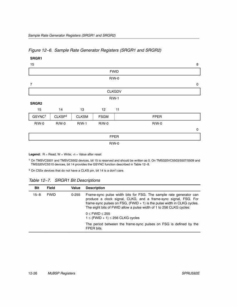
Sample Rate Generator Registers (SRGR1 and SRGR2)
McBSP Registers12-26 SPRU592E
Figure 12−6. Sample Rate Generator Registers (SRGR1 and SRGR2)
SRGR1
15 8
FWID
R/W-0
7 0
CLKGDV
R/W-1
SRGR2
15 14 13 12 11
GSYNC† CLKSP‡ CLKSM FSGM FPER
R/W-0 R/W-0 R/W-1 R/W-0 R/W-0
0
FPER
R/W-0
Legend: R = Read; W = Write; -n = Value after reset
† On TMSVC5501 and TMSVC5502 devices, bit 15 is reserved and should be written as 0. On TMS320VC5503/5507/5509 andTMS320VC5510 devices, bit 14 provides the GSYNC function described in Table 12−8.
‡ On C55x devices that do not have a CLKS pin, bit 14 is a don’t care.
Table 12−7. SRGR1 Bit Descriptions
Bit Field Value Description
15–8 FWID 0-255 Frame-sync pulse width bits for FSG. The sample rate generator canproduce a clock signal, CLKG, and a frame-sync signal, FSG. Forframe-sync pulses on FSG, (FWID + 1) is the pulse width in CLKG cycles.The eight bits of FWID allow a pulse width of 1 to 256 CLKG cycles:
0 ≤ FWID ≤ 2551 ≤ (FWID + 1) ≤ 256 CLKG cycles
The period between the frame-sync pulses on FSG is defined by theFPER bits.

Sample Rate Generator Registers (SRGR1 and SRGR2)
12-27McBSP RegistersSPRU592E
Table 12−7. SRGR1 Bit Descriptions (Continued)
Bit DescriptionValueField
7–0 CLKGDV 0-255 Divide-down value for CLKG. The sample rate generator can accept aninput clock signal and divide it down according to CLKGDV to produce anoutput clock signal, CLKG. The frequency of CLKG is:
CLKG frequency = (Input clock frequency) / (CLKGDV + 1)
The input clock is selected by the SCLKME and CLKSM bits:
SCLKME CLKSMInput Clock ForSample Rate Generator
0 0 Signal on CLKS pin
0 1 McBSP internal input clock
1 0 Signal on CLKR pin
1 1 Signal on CLKX pin
A DSP reset forces the CLKG frequency to 1/2 the input clock frequency(CLKGDV = 1), and the reset selects the McBSP internal input clock as theinput clock.
The maximum frequency for the McBSP on theTMS320VC5503/5507/5509 and TMS320VC5510 devices is 1/2 the CPUclock frequency. The maximum frequency for the McBSP on theTMS320VC5501 and TMS320VC5502 devices is 1/2 the frequency of theslow peripherals clock. See the device-specific data manual for timingrequirements for the McBSP.
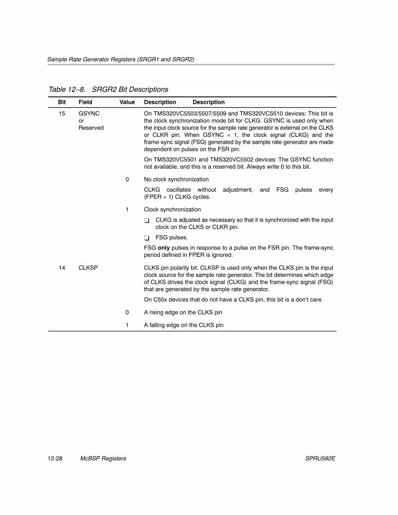
Sample Rate Generator Registers (SRGR1 and SRGR2)
McBSP Registers12-28 SPRU592E
Table 12−8. SRGR2 Bit Descriptions
Bit Field Value Description Description
15 GSYNCorReserved
On TMS320VC5503/5507/5509 and TMS320VC5510 devices: This bit isthe clock synchronization mode bit for CLKG. GSYNC is used only whenthe input clock source for the sample rate generator is external on the CLKSor CLKR pin. When GSYNC = 1, the clock signal (CLKG) and theframe-sync signal (FSG) generated by the sample rate generator are madedependent on pulses on the FSR pin.
On TMS320VC5501 and TMS320VC5502 devices: The GSYNC functionnot available, and this is a reserved bit. Always write 0 to this bit.
0 No clock synchronization
CLKG oscillates without adjustment, and FSG pulses every(FPER + 1) CLKG cycles.
1 Clock synchronization
� CLKG is adjusted as necessary so that it is synchronized with the inputclock on the CLKS or CLKR pin.
� FSG pulses.
FSG only pulses in response to a pulse on the FSR pin. The frame-syncperiod defined in FPER is ignored.
14 CLKSP CLKS pin polarity bit. CLKSP is used only when the CLKS pin is the inputclock source for the sample rate generator. The bit determines which edgeof CLKS drives the clock signal (CLKG) and the frame-sync signal (FSG)that are generated by the sample rate generator.
On C55x devices that do not have a CLKS pin, this bit is a don’t care.
0 A rising edge on the CLKS pin
1 A falling edge on the CLKS pin

Sample Rate Generator Registers (SRGR1 and SRGR2)
12-29McBSP RegistersSPRU592E
Table 12−8. SRGR2 Bit Descriptions (Continued)
Bit DescriptionDescriptionValueField
13 CLKSM Sample rate generator input clock mode bit. The sample rate generator canaccept an input clock signal and divide it down according to CLKGDV toproduce an output clock signal, CLKG. The frequency of CLKG is:
CLKG frequency = (Input clock frequency) / (CLKGDV + 1)
CLKSM is used in conjunction with the SCLKME bit to determine the sourcefor the input clock.
A DSP reset selects the McBSP internal input clock as the input clock andforces the CLKG frequency to 1/2 the McBSP internal input clock frequency.
0 The input clock for the sample rate generator is taken from the CLKS pin orfrom the CLKR pin, depending on the value of the SCLKME bit of PCR:
SCLKME CLKSMInput Clock ForSample Rate Generator
0 0 Signal on CLKS pin
1 0 Signal on CLKR pin
1 The input clock for the sample rate generator is taken from the McBSPinternal input clock or from the CLKX pin, depending on the value of theSCLKME bit of PCR:
SCLKME CLKSMInput Clock ForSample Rate Generator
0 1 McBSP internal input clock
1 1 Signal on CLKX pin

Sample Rate Generator Registers (SRGR1 and SRGR2)
McBSP Registers12-30 SPRU592E
Table 12−8. SRGR2 Bit Descriptions (Continued)
Bit DescriptionDescriptionValueField
12 FSGM Sample rate generator transmit frame-sync mode bit. The transmitter canget frame synchronization from the FSX pin (FSXM = 0) or from inside theMcBSP (FSXM = 1). When FSXM = 1, the FSGM bit determines how theMcBSP supplies frame-sync pulses.
0 If FSXM = 1, the McBSP generates a transmit frame-sync pulse when thecontent of DXR[1,2] is copied to XSR[1,2].
1 If FSXM = 1, the transmitter uses frame-sync pulses generated by thesample rate generator. Program the FWID bits to set the width of eachpulse. Program the FPER bits to set the period between pulses.
11–0 FPER 0–4095 Frame-sync period bits for FSG. The sample rate generator can produce aclock signal, CLKG, and a frame-sync signal, FSG. The period betweenframe-sync pulses on FSG is (FPER + 1) CLKG cycles. The 12 bits ofFPER allow a frame-sync period of 1 to 4096 CLKG cycles:
0 ≤ FPER ≤ 40951 ≤ (FPER + 1) ≤ 4096 CLKG cycles
The width of each frame-sync pulse on FSG is defined by the FWID bits.

Multichannel Control Registers (MCR1 and MCR2)
12-31McBSP RegistersSPRU592E
12.7 Multichannel Control Registers (MCR1 and MCR2)
Each McBSP has two multichannel control registers of the form shown inFigure 12−7. MCR1 has control and status bits (with an R prefix) formultichannel selection operation in the receiver. MCR2 contains the sametype of bits (bit with an X prefix) for the transmitter. The bits of MCR1 and MCR2are described in Table 12−9 and Table 12−10, respectively. TheseI/O-mapped registers enable you to:
� Enable all channels or only selected channels for reception (RMCM)
� Choose which channels are enabled/disabled and masked/unmasked fortransmission (XMCM)
� Specify whether two partitions (32 channels at a time) or eight partitions(128 channels at a time) can be used (RMCME for reception, XMCME fortransmission)
� Assign blocks of 16 channels to partitions A and B when the 2-partitionmode is selected (RPABLK and RPBBLK for reception, XPABLK andXPBBLK for transmission)
� Determine which block of 16 channels is currently involved in a datatransfer (RCBLK for reception, XCBLK for transmission)
Figure 12−7. Multichannel Control Registers (MCR1 and MCR2)
MCR1
15 10 9 8
Reserved RMCME RPBBLK
R-0 R/W-0 R/W-00
7 6 5 4 2 1 0
RPBBLK RPABLK RCBLK Reserved RMCM
R/W-00 R/W-00 R-000 R-0 R/W-0
MCR2
15 10 9 8
Reserved XMCME XPBBLK
R-0 R/W-0 R/W-00
7 6 5 4 2 1 0
XPBBLK XPABLK XCBLK XMCM
R/W-00 R/W-00 R-000 R/W-00
Legend: R = Read; W = Write; -n = Value after reset

Multichannel Control Registers (MCR1 and MCR2)
McBSP Registers12-32 SPRU592E
Table 12−9. MCR1 Bit Descriptions
Bit Field Value Description
15-10 Reserved 0 Reserved bits (not available for your use). They are read-only bits andreturn 0s when read.
9 RMCME Receive multichannel partition mode bit. RMCME is only applicable ifchannels can be individually enabled or disabled for reception (RMCM = 1).
RMCME determines whether only 32 channels or all 128 channels are tobe individually selectable.
0 2-partition mode
Only partitions A and B are used. You can control up to 32 channels in thereceive multichannel selection mode (RMCM = 1).
Assign 16 channels to partition A with the RPABLK bits. Assign 16 channelsto partition B with the RPBBLK bits.
You control the channels with the appropriate receive channel enableregisters:RCERA: Channels in partition ARCERB: Channels in partition B
1 8-partition mode
All partitions (A through H) are used. You can control up to 128 channels inthe receive multichannel selection mode.
You control the channels with the appropriate receive channel enableregisters:RCERA: Channels 0 through 15RCERB: Channels 16 through 31RCERC: Channels 32 through 47RCERD: Channels 48 through 63RCERE: Channels 64 through 79RCERF: Channels 80 through 95RCERG: Channels 96 through 111RCERH: Channels 112 through 127

Multichannel Control Registers (MCR1 and MCR2)
12-33McBSP RegistersSPRU592E
Table 12−9. MCR1 Bit Descriptions (Continued)
Bit DescriptionValueField
8–7 RPBBLK Receive partition B block bits
RPBBLK is only applicable if channels can be individually enabled ordisabled (RMCM = 1) and the 2-partition mode is selected (RMCME = 0).Under these conditions, the McBSP receiver can accept or ignore data inany of the 32 channels that are assigned to partitions A and B of the receiver.
The 128 receive channels of the McBSP are divided equally among 8 blocks(0 through 7). When RPBBLK is applicable, use RPBBLK to assign one ofthe odd-numbered blocks (1, 3, 5, or 7) to partition B. Use the RPABLK bitsto assign one of the even-numbered blocks (0, 2, 4, or 6) to partition A.
If you want to use more than 32 channels, you can change blockassignments dynamically. You can assign a new block to one partition whilethe receiver is handling activity in the other partition. For example, while theblock in partition A is active, you can change which block is assigned topartition B. The RCBLK bits are regularly updated to indicate which blockis active.
Note: When XMCM = 11b (for symmetric transmission and reception), thetransmitter uses the receive block bits (RPABLK and RPBBLK) rather thanthe transmit block bits (XPABLK and XPBBLK).
00b Block 1: channels 16 through 31
01b Block 3: channels 48 through 63
10b Block 5: channels 80 through 95
11b Block 7: channels 112 through 127
6–5 RPABLK Receive partition A block bits
RPABLK is only applicable if channels can be individually enabled ordisabled (RMCM = 1) and the 2-partition mode is selected (RMCME = 0).Under these conditions, the McBSP receiver can accept or ignore data inany of the 32 channels that are assigned to partitions A and B of the receiver.See the description for RPBBLK (bits 8-7) for more information aboutassigning blocks to partitions A and B.
00b Block 0: channels 0 through 15
01b Block 2: channels 32 through 47
10b Block 4: channels 64 through 79
11b Block 6: channels 96 through 111

Multichannel Control Registers (MCR1 and MCR2)
McBSP Registers12-34 SPRU592E
Table 12−9. MCR1 Bit Descriptions (Continued)
Bit DescriptionValueField
4–2 RCBLK Receive current block indicator. RCBLK indicates which block of16 channels is involved in the current McBSP reception:
000b Block 0: channels 0 through 15
001b Block 1: channels 16 through 31
010b Block 2: channels 32 through 47
011b Block 3: channels 48 through 63
100b Block 4: channels 64 through 79
101b Block 5: channels 80 through 95
110b Block 6: channels 96 through 111
111b Block 7: channels 112 through 127
1 Reserved 0 Reserved bits (not available for your use). They are read-only bits andreturn 0s when read.
0 RMCM Receive multichannel selection mode bit. RMCM determines whether allchannels or only selected channels are enabled for reception:
0 All 128 channels are enabled.
1 Multichannel selection mode. Channels can be individually enabled ordisabled.
The only channels enabled are those selected in the appropriate receivechannel enable registers (RCERs). The way channels are assigned to theRCERs depends on the number of receive channel partitions (2 or 8), asdefined by the RMCME bit.
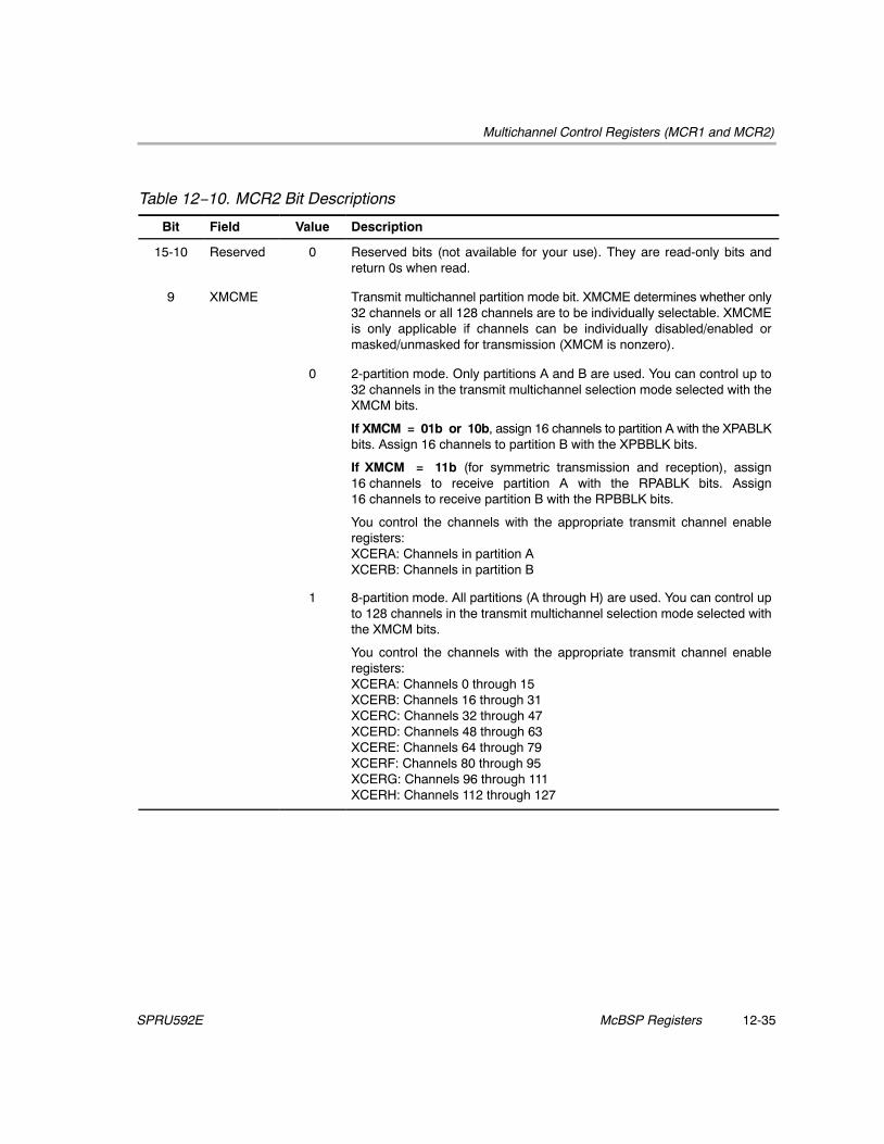
Multichannel Control Registers (MCR1 and MCR2)
12-35McBSP RegistersSPRU592E
Table 12−10. MCR2 Bit Descriptions
Bit Field Value Description
15-10 Reserved 0 Reserved bits (not available for your use). They are read-only bits andreturn 0s when read.
9 XMCME Transmit multichannel partition mode bit. XMCME determines whether only32 channels or all 128 channels are to be individually selectable. XMCMEis only applicable if channels can be individually disabled/enabled ormasked/unmasked for transmission (XMCM is nonzero).
0 2-partition mode. Only partitions A and B are used. You can control up to32 channels in the transmit multichannel selection mode selected with theXMCM bits.
If XMCM = 01b or 10b, assign 16 channels to partition A with the XPABLKbits. Assign 16 channels to partition B with the XPBBLK bits.
If XMCM = 11b (for symmetric transmission and reception), assign16 channels to receive partition A with the RPABLK bits. Assign16 channels to receive partition B with the RPBBLK bits.
You control the channels with the appropriate transmit channel enableregisters:XCERA: Channels in partition AXCERB: Channels in partition B
1 8-partition mode. All partitions (A through H) are used. You can control upto 128 channels in the transmit multichannel selection mode selected withthe XMCM bits.
You control the channels with the appropriate transmit channel enableregisters:XCERA: Channels 0 through 15XCERB: Channels 16 through 31XCERC: Channels 32 through 47XCERD: Channels 48 through 63XCERE: Channels 64 through 79XCERF: Channels 80 through 95XCERG: Channels 96 through 111XCERH: Channels 112 through 127
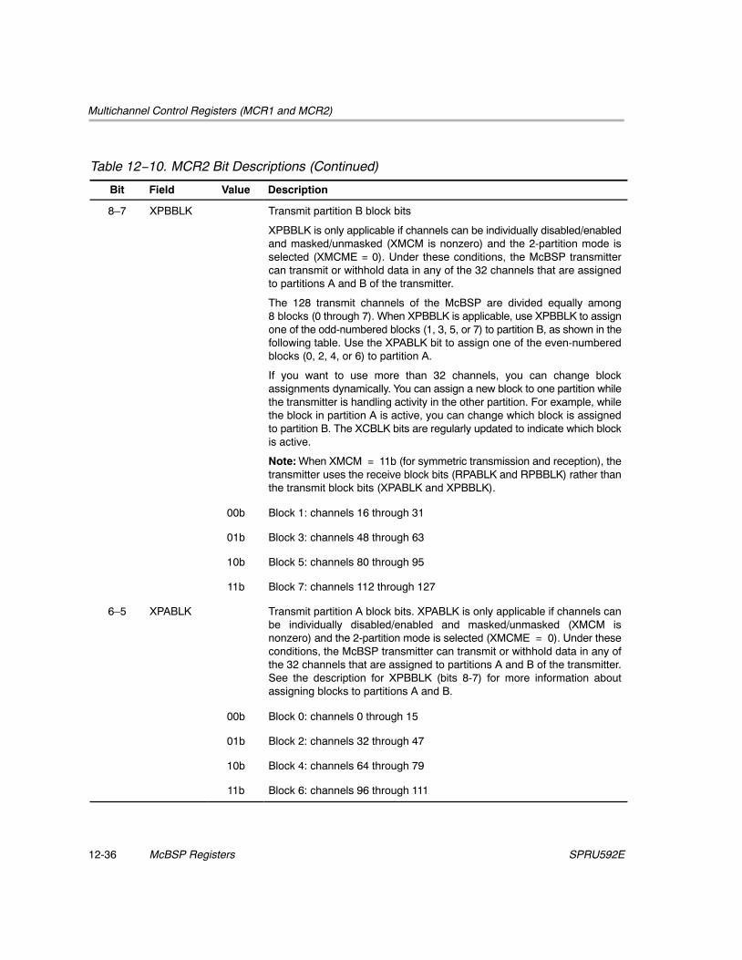
Multichannel Control Registers (MCR1 and MCR2)
McBSP Registers12-36 SPRU592E
Table 12−10. MCR2 Bit Descriptions (Continued)
Bit DescriptionValueField
8–7 XPBBLK Transmit partition B block bits
XPBBLK is only applicable if channels can be individually disabled/enabledand masked/unmasked (XMCM is nonzero) and the 2-partition mode isselected (XMCME = 0). Under these conditions, the McBSP transmittercan transmit or withhold data in any of the 32 channels that are assignedto partitions A and B of the transmitter.
The 128 transmit channels of the McBSP are divided equally among8 blocks (0 through 7). When XPBBLK is applicable, use XPBBLK to assignone of the odd-numbered blocks (1, 3, 5, or 7) to partition B, as shown in thefollowing table. Use the XPABLK bit to assign one of the even-numberedblocks (0, 2, 4, or 6) to partition A.
If you want to use more than 32 channels, you can change blockassignments dynamically. You can assign a new block to one partition whilethe transmitter is handling activity in the other partition. For example, whilethe block in partition A is active, you can change which block is assignedto partition B. The XCBLK bits are regularly updated to indicate which blockis active.
Note: When XMCM = 11b (for symmetric transmission and reception), thetransmitter uses the receive block bits (RPABLK and RPBBLK) rather thanthe transmit block bits (XPABLK and XPBBLK).
00b Block 1: channels 16 through 31
01b Block 3: channels 48 through 63
10b Block 5: channels 80 through 95
11b Block 7: channels 112 through 127
6–5 XPABLK Transmit partition A block bits. XPABLK is only applicable if channels canbe individually disabled/enabled and masked/unmasked (XMCM isnonzero) and the 2-partition mode is selected (XMCME = 0). Under theseconditions, the McBSP transmitter can transmit or withhold data in any ofthe 32 channels that are assigned to partitions A and B of the transmitter.See the description for XPBBLK (bits 8-7) for more information aboutassigning blocks to partitions A and B.
00b Block 0: channels 0 through 15
01b Block 2: channels 32 through 47
10b Block 4: channels 64 through 79
11b Block 6: channels 96 through 111

Multichannel Control Registers (MCR1 and MCR2)
12-37McBSP RegistersSPRU592E
Table 12−10. MCR2 Bit Descriptions (Continued)
Bit DescriptionValueField
4–2 XCBLK Transmit current block indicator. XCBLK indicates which block of16 channels is involved in the current McBSP transmission:
000b Block 0: channels 0 through 15
001b Block 1: channels 16 through 31
010b Block 2: channels 32 through 47
011b Block 3: channels 48 through 63
100b Block 4: channels 64 through 79
101b Block 5: channels 80 through 95
110b Block 6: channels 96 through 111
111b Block 7: channels 112 through 127
1–0 XMCM Transmit multichannel selection mode bits. XMCM determines whether allchannels or only selected channels are enabled and unmasked fortransmission.
00b Transmit multichannel selection is off. All channels are enabled andunmasked. No channels can be disabled or masked.
01b All channels are disabled unless they are selected in the appropriatetransmit channel enable registers (XCERs). If enabled, a channel in thismode is also unmasked.
The XMCME bit determines whether 32 channels or 128 channels areselectable in XCERs.
10b All channels are enabled, but they are masked unless they are selected inthe appropriate transmit channel enable registers (XCERs).
The XMCME bit determines whether 32 channels or 128 channels areselectable in XCERs.
11b This mode is used for symmetric transmission and reception.
All channels are disabled for transmission unless they are enabled forreception in the appropriate receive channel enable registers (RCERs).Once enabled, they are masked unless they are also selected in theappropriate transmit channel enable registers (XCERs).
The XMCME bit determines whether 32 channels or 128 channels areselectable in RCERs and XCERs.

Pin Control Register (PCR)
McBSP Registers12-38 SPRU592E
12.8 Pin Control Register (PCR)
Each McBSP has one pin control register of the form shown in Figure 12−8.Table 12−11 describes the bits of PCR. This I/O-mapped register enables youto:
� Allow the McBSP to enter a low-power mode when the idle instruction isexecuted (IDLEEN, in conjunction with the PERI bit of ICR). For theTMS320VC5503/5507/5509 and TMS320VC5510 devices, this capabilityis provided in the PCR. On the TMS320VC5501 and TMS320VC5502devices, this capability is provided in the Peripheral Idle Control Register(PICR). For more information on the TMS320VC5501 implementation,see the TMS320VC5501 Fixed-Point Digital Signal Processor DataManual (literature number SPRS206); for the TMS320VC5502implementation, see the TMS320VC5502 Fixed-Point Digital SignalProcessor Data Manual (literature number SPRS166).
� Specify whether McBSP pins can be used as general-purpose I/O pinswhen the transmitter and/or receiver is in its reset state (XIOEN andRIOEN)
� Choose a frame-sync mode for the transmitter (FSXM) and for the receiver(FSRM)
� Choose a clock mode for transmitter (CLKXM) and for the receiver(CLKRM)
� Select the input clock source for the sample rate generator (SCLKME, inconjunction with the CLKSM bit of SRGR2)
� Read or write data when the CLKS, DX, and DR pins are configured asgeneral-purpose I/O pins (CLKSSTAT, DXSTAT, and DXSTAT)
� Choose whether frame-sync signals are active low or active high (FSXPfor transmission, FSRP for reception)
� Specify whether data is sampled on the falling edge or the rising edge ofthe clock signals (CLKXP for transmission, CLKRP for reception)

Pin Control Register (PCR)
12-39McBSP RegistersSPRU592E
Figure 12−8. Pin Control Register (PCR)
15 14 13 12 11 10 9 8
Reserved IDLEEN† XIOEN RIOEN FSXM FSRM CLKXM CLKRM
R-0 R/W-0 R/W-0 R/W-0 R/W-0 R/W-0 R/W-0 R/W-0
7 6 5 4 3 2 1 0
SCLKME CLKSSTAT DXSTAT DRSTAT FSXP FSRP CLKXP CLKRP
R/W-0 R-0 R/W-0 R-0 R/W-0 R/W-0 R/W-0 R/W-0
Legend: R = Read; W = Write; -n = Value after reset† On TMSVC5501 and TMSVC5502 devices, bit 14 is reserved and should be written as 0. On TMS320VC5503/5507/5509 and
TMS320VC5510 devices, bit 14 provides the IDLEEN function described in Table 12−11.
Table 12−11. PCR Bit Descriptions
Bit Field Value Description
15 Reserved 0 Reserved bit (not available for your use). It is a read-only bit and returns a0 when read.
14 IDLEENorReserved
On TMS320VC5503/5507/5509 and TMS320VC5510 devices: This bit isthe idle enable bit. If the PERIPH idle domain is configured to be idle andIDLEEN = 1, the McBSP stops and enters a low-power state.
On the TMS320VC5501 and TMS320VC5502 devices: This bit is reservedand should be written as 0. The IDLEEN function is implemented in thePeripheral Idle Control Register (PICR). For more information on the PICR,see the TMS320VC5501 Fixed-Point Digital Signal Processor Data Manual(literature number SPRS206) or the TMS320VC5502 Fixed-Point DigitalSignal Processor Data Manual (literature number SPRS166).
0 The McBSP remains active when the PERIPH domain is idled.
1 If the PERIPH domain is idle (PERIS = 1 in the idle status register), theMcBSP is stopped in a low-power state.
13 XIOEN Transmit I/O enable bit. When the transmitter is in reset (XRST = 0), XIOENcan configure certain McBSP pins as general-purpose I/O (GPIO) pins. Fora summary, see the table that follows the RIOEN bit description.
0 The CLKX, FSX, DX, and CLKS pins are serial port pins.
1 If XRST = 0, the CLKX, FSX, and DX pins are GPIO pins. The CLKS is alsoa GPIO pin if RRST = 0 and RIOEN = 1.

Pin Control Register (PCR)
McBSP Registers12-40 SPRU592E
Table 12−11. PCR Bit Descriptions (Continued)
Bit DescriptionValueField
12 RIOEN Receive I/O enable bit. When the receiver is in reset (RRST = 0), RIOENcan configure certain McBSP pins as general-purpose I/O (GPIO) pins . Fora summary, see the table that follows the RIOEN bit description. XRST andRRST are in the serial port control registers, but all other bits mentioned inthis table are in the pin control register.
0 The CLKR, FSR, DR, and CLKS pins are serial port pins.
1 If RRST = 0, the CLKR, FSR, and DR pins are GPIO pins. The CLKS is alsoa GPIO pin if XRST = 0 and XIOEN = 1.
Pin
General Purpose UseEnabled by This BitCombination
Selected asOutput When …
Output ValueDriven FromThis Bit
Selected AsInput When …
Input ValueRead FromThis Bit
CLKX XRST = 0XIOEN = 1
CLKXM = 1 CLKXP CLKXM = 0 CLKXP
FSX XRST = 0XIOEN = 1
FSXM = 1 FSXP FSXM = 0 FSXP
DX XRST = 0XIOEN = 1
Always DXSTAT Never Does not apply
CLKR RRST = 0RIOEN = 1
CLKRM = 1 CLKRP CLKRM = 0 CLKRP
FSR RRST = 0RIOEN = 1
FSRM = 1 FSRP FSRM = 0 FSRP
DR RRST = 0RIOEN = 1
Never Does not apply Always DRSTAT
CLKS RRST = XRST = 0RIOEN = XIOEN = 1
Never Does not apply Always CLKSSTAT

Pin Control Register (PCR)
12-41McBSP RegistersSPRU592E
Table 12−11.PCR Bit Descriptions (Continued)
Bit Field Value Description
11 FSXM Transmit frame-sync mode bit. FSXM determines whether transmitframe-sync pulses are supplied externally or internally. The polarity of thesignal on the FSX pin is determined by the FSXP bit.
0 Transmit frame synchronization is supplied by an external source via theFSX pin.
1 Transmit frame synchronization is supplied by the McBSP, as determinedby the FSGM bit of SRGR2.
10 FSRM Receive frame-sync mode bit. FSRM determines whether receiveframe-sync pulses are supplied externally or internally. The polarity of thesignal on the FSR pin is determined by the FSRP bit.
0 Receive frame synchronization is supplied by an external source via theFSR pin.
1 Receive frame synchronization is supplied by the sample rate generator.FSR is an output pin reflecting internal FSR, except when GSYNC = 1 inSRGR2.
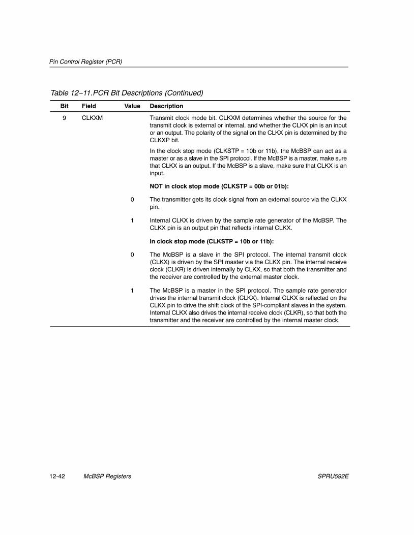
Pin Control Register (PCR)
McBSP Registers12-42 SPRU592E
Table 12−11.PCR Bit Descriptions (Continued)
Bit Field Value Description
9 CLKXM Transmit clock mode bit. CLKXM determines whether the source for thetransmit clock is external or internal, and whether the CLKX pin is an inputor an output. The polarity of the signal on the CLKX pin is determined by theCLKXP bit.
In the clock stop mode (CLKSTP = 10b or 11b), the McBSP can act as amaster or as a slave in the SPI protocol. If the McBSP is a master, make surethat CLKX is an output. If the McBSP is a slave, make sure that CLKX is aninput.
NOT in clock stop mode (CLKSTP = 00b or 01b):
0 The transmitter gets its clock signal from an external source via the CLKXpin.
1 Internal CLKX is driven by the sample rate generator of the McBSP. TheCLKX pin is an output pin that reflects internal CLKX.
In clock stop mode (CLKSTP = 10b or 11b):
0 The McBSP is a slave in the SPI protocol. The internal transmit clock(CLKX) is driven by the SPI master via the CLKX pin. The internal receiveclock (CLKR) is driven internally by CLKX, so that both the transmitter andthe receiver are controlled by the external master clock.
1 The McBSP is a master in the SPI protocol. The sample rate generatordrives the internal transmit clock (CLKX). Internal CLKX is reflected on theCLKX pin to drive the shift clock of the SPI-compliant slaves in the system.Internal CLKX also drives the internal receive clock (CLKR), so that both thetransmitter and the receiver are controlled by the internal master clock.

Pin Control Register (PCR)
12-43McBSP RegistersSPRU592E
Table 12−11.PCR Bit Descriptions (Continued)
Bit Field Value Description
8 CLKRM Receive clock mode bit. The role of CLKRM and the resulting effect on theCLKR pin depend on whether the McBSP is in the digital loopback mode(DLB = 1).
Note: The polarity of the signal on the CLKR pin is determined by theCLKRP bit.
NOT in digital loopback mode (DLB = 0):
0 The CLKR pin is an input pin that supplies the internal receive clock (CLKR).
1 Internal CLKR is driven by the sample rate generator of the McBSP. TheCLKR pin is an output pin that reflects internal CLKR.
In digital loopback mode (DLB = 1):
0 The CLKR pin is in the high impedance state. The internal receive clock(CLKR) is driven by the internal transmit clock (CLKX). CLKX is derivedaccording to the CLKXM bit.
1 Internal CLKR is driven by internal CLKX. The CLKR pin is an output pin thatreflects internal CLKR. CLKX is derived according to the CLKXM bit.

Pin Control Register (PCR)
McBSP Registers12-44 SPRU592E
Table 12−11.PCR Bit Descriptions (Continued)
Bit DescriptionValueField
7 SCLKME Sample rate generator input clock mode bit. The sample rate generator canproduce a clock signal, CLKG. The frequency of CLKG is:
CLKG freq. = (Input clock frequency) / (CLKGDV + 1)
SCLKME is used in conjunction with the CLKSM bit to select the input clock.
0 The input clock for the sample rate generator is taken from the CLKS pin orfrom the McBSP internal input clock, depending on the value of the CLKSMbit of SRGR2:
SCLKME CLKSMInput Clock ForSample Rate Generator
0 0 Signal on CLKS pin
0 1 McBSP internal input clock
1 The input clock for the sample rate generator is taken from the CLKR pinor from the CLKX pin, depending on the value of the CLKSM bit of SRGR2:
SCLKME CLKSMInput Clock ForSample Rate Generator
1 0 Signal on CLKR pin
1 1 Signal on CLKX pin
6 CLKSSTAT CLKS pin status bit. When CLKSSTAT is applicable, it reflects the level onthe CLKS pin.
CLKSSTAT is only applicable when the transmitter and receiver are both inreset (XRST = RRST = 0) and CLKS is configured for use as ageneral-purpose input pin (XIOEN = RIOEN = 1).
0 The signal on the CLKS pin is low.
1 The signal on the CLKS pin is high.
5 DXSTAT DX pin status bit. When DXSTAT is applicable, you can toggle the signal onDX by writing to DXSTAT.
DXSTAT is only applicable when the transmitter is in reset (XRST = 0) andDX is configured for use as a general-purpose output pin (XIOEN = 1).
0 Drive the signal on the DX pin low.
1 Drive the signal on the DX pin high.

Pin Control Register (PCR)
12-45McBSP RegistersSPRU592E
Table 12−11.PCR Bit Descriptions (Continued)
Bit DescriptionValueField
4 DRSTAT DR pin status bit. When DRSTAT is applicable, it reflects the level on theDR pin.
DRSTAT is only applicable when the receiver is in reset (RRST = 0) and DRis configured for use as a general-purpose input pin (RIOEN = 1).
0 The signal on DR pin is low.
1 The signal on DR pin is high.
3 FSXP Transmit frame-sync polarity bit. FSXP determines the polarity of FSX asseen on the FSX pin.
0 Transmit frame-sync pulses are active high.
1 Transmit frame-sync pulses are active low.
2 FSRP Receive frame-sync polarity bit. FSRP determines the polarity of FSR asseen on the FSR pin.
0 Receive frame-sync pulses are active high.
1 Receive frame-sync pulses are active low.
1 CLKXP Transmit clock polarity bit. CLKXP determines the polarity of CLKX as seenon the CLKX pin. This bit also can effect the sample rate generator (seesection 3.1 on page 3-2) and effects the clock stop mode (see Chapter 6).
0 Transmit data is driven on the rising edge of CLKX.
1 Transmit data is driven on the falling edge of CLKX.
0 CLKRP Receive clock polarity bit. CLKRP determines the polarity of CLKR as seenon the CLKR pin. This bit also can effect the sample rate generator (seesection 3.1 on page 3-2) and effects the clock stop mode (see Chapter 6).
0 When the CLKR pin is configured as an input, the external CLKR is notinverted before being used internally and the receive data is sampled on thefalling edge of CLKR.
When the CLKR pin is configured an as output, the internal CLKR is notinverted before being driven on the pin.
1 When the CLKR pin is configured as an input, the external CLKR is invertedbefore being used internally and the receive data is sampled on the risingedge of CLKR.
When the CLKR pin is configured an as output, the internal CLKR is invertedbefore being driven on the pin.

Receive Channel Enable Registers (RCERA-RCERH)
McBSP Registers12-46 SPRU592E
12.9 Receive Channel Enable Registers (RCERA-RCERH)
Each McBSP has eight receive channel enable registers of the format shownin Figure 12−9. There is one for each of the receive partitions: A, B, C, D, E,F, G, and H. Table 12−12 provides a summary description that applies to anybit x of a receive channel enable register.
These I/O-mapped registers are only used when the receiver is configured toallow individual enabling and disabling of the channels (RMCM = 1).
Figure 12−9. Format of the Receive Channel Enable Registers (RCERA-RCERH)
15 14 13 12 11 10 9 8
RCE15 RCE14 RCE13 RCE12 RCE11 RCE10 RCE9 RCE8
R/W-0 R/W-0 R/W-0 R/W-0 R/W-0 R/W-0 R/W-0 R/W-0
7 6 5 4 3 2 1 0
RCE7 RCE6 RCE5 RCE4 RCE3 RCE2 RCE1 RCE0
R/W-0 R/W-0 R/W-0 R/W-0 R/W-0 R/W-0 R/W-0 R/W-0
Legend: R = Read; W = Write; -n = Value after reset
Table 12−12. Description For Bit x of a Receive Channel Enable Register(x = 0, 1, 2, ..., or 15)
Bit Field Value Description
x RCEx Receive channel enable bit
For receive multichannel selection mode (RMCM = 1):
0 Disable the channel that is mapped to RCEx.
1 Enable the channel that is mapped to RCEx.

Receive Channel Enable Registers (RCERA-RCERH)
12-47McBSP RegistersSPRU592E
12.9.1 RCERs Used in the Receive Multichannel Selection Mode
For multichannel selection operation, the assignment of channels to theRCERs depends on whether 32 or 128 channels are individually selectable,as defined by the RMCME bit. For each of these two cases, Table 12−13shows which block of channels is assigned to each of the RCERs used. Foreach RCER, the table shows which channel is assigned to each of the bits.
Table 12−13. Use of the Receive Channel Enable Registers
Number ofS l t bl
Block Assignments Channel AssignmentsSelectableChannels RCERx Block Assigned Bit in RCERx Channel Assigned
32(RMCME = 0)
RCERA Channels n to (n + 15)
The block of channels ischosen with the RPABLKbits.
RCE0RCE1RCE2:RCE15
Channel nChannel (n + 1)Channel (n + 2):Channel (n + 15)
RCERB Channels m to (m + 15)
The block of channels ischosen with the RPBBLKbits.
RCE0RCE1RCE2:RCE15
Channel mChannel (m + 1)Channel (m + 2):Channel (m + 15)
128(RMCME = 1)
RCERA Block 0 RCE0RCE1RCE2:RCE15
Channel 0Channel 1Channel 2:Channel 15
RCERB Block 1 RCE0RCE1RCE2:RCE15
Channel 16Channel 17Channel 18:Channel 31
RCERC Block 2 RCE0RCE1RCE2:RCE15
Channel 32Channel 33Channel 34:Channel 47
RCERD Block 3 RCE0RCE1RCE2:RCE15
Channel 48Channel 49Channel 50:Channel 63
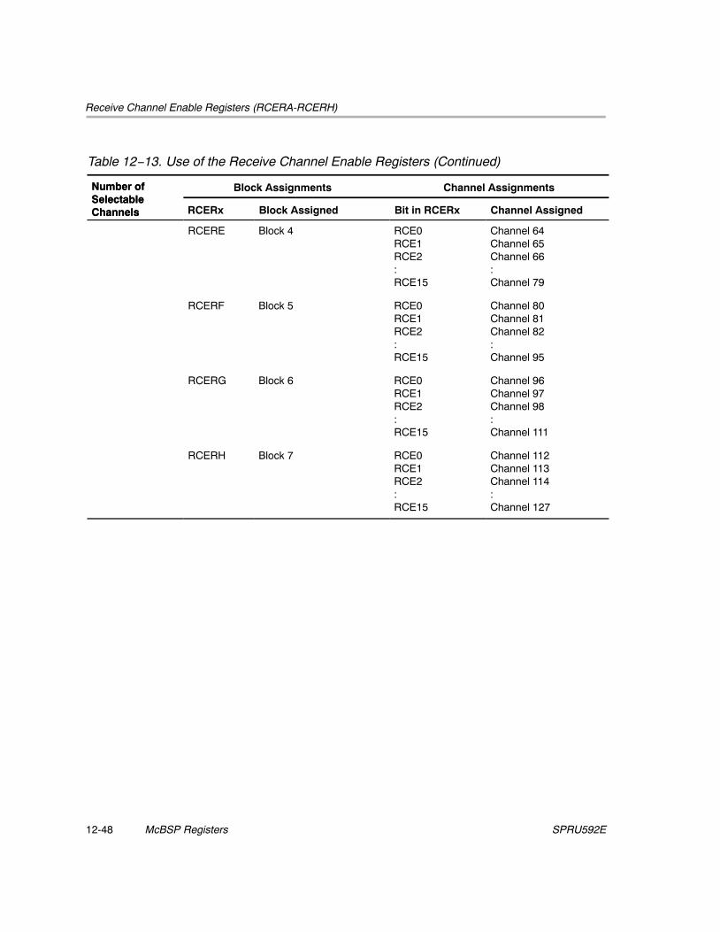
Receive Channel Enable Registers (RCERA-RCERH)
McBSP Registers12-48 SPRU592E
Table 12−13. Use of the Receive Channel Enable Registers (Continued)
Number ofSelectableChannels
Channel AssignmentsBlock AssignmentsNumber ofSelectableChannels Channel AssignedBit in RCERxBlock AssignedRCERx
RCERE Block 4 RCE0RCE1RCE2:RCE15
Channel 64Channel 65Channel 66:Channel 79
RCERF Block 5 RCE0RCE1RCE2:RCE15
Channel 80Channel 81Channel 82:Channel 95
RCERG Block 6 RCE0RCE1RCE2:RCE15
Channel 96Channel 97Channel 98:Channel 111
RCERH Block 7 RCE0RCE1RCE2:RCE15
Channel 112Channel 113Channel 114:Channel 127

Transmit Channel Enable Registers (XCERA-XCERH)
12-49McBSP RegistersSPRU592E
12.10 Transmit Channel Enable Registers (XCERA-XCERH)
Each McBSP has eight transmit channel enable registers of the form shownin Figure 12−10. There is one for each of the transmit partitions: A, B, C, D, E,F, G, and H. Table 12−14 provides a summary description that applies to eachbit XCEx of a transmit channel enable register.
The I/O-mapped XCERs are only used when the transmitter is configured toallow individual disabling/enabling and masking/unmasking of the channels(XMCM is nonzero).
Figure 12−10. Format of the Transmit Channel Enable Registers (XCERA-XCERH)
15 14 13 12 11 10 9 8
XCE15 XCE14 XCE13 XCE12 XCE11 XCE10 XCE9 XCE8
R/W-0 R/W-0 R/W-0 R/W-0 R/W-0 R/W-0 R/W-0 R/W-0
7 6 5 4 3 2 1 0
XCE7 XCE6 XCE5 XCE4 XCE3 XCE2 XCE1 XCE0
R/W-0 R/W-0 R/W-0 R/W-0 R/W-0 R/W-0 R/W-0 R/W-0
Legend: R = Read; W = Write; -n = Value after reset

Transmit Channel Enable Registers (XCERA-XCERH)
McBSP Registers12-50 SPRU592E
Table 12−14. Description For Bit x of a Transmit Channel Enable Register(x = 0, 1, 2, ..., or 15)
Bit Field Value Description
x XCEx Transmit channel enable bit. The role of this bit depends on which transmitmultichannel selection mode is selected with the XMCM bits.
For multichannel selection when XMCM = 01b(all channels disabled unless selected):
0 Disable and mask the channel that is mapped to XCEx.
1 Enable and unmask the channel that is mapped to XCEx.
For multichannel selection when XMCM = 10b(all channels enabled but masked unless selected):
0 Mask the channel that is mapped to XCEx.
1 Unmask the channel that is mapped to XCEx.
For multichannel selection when XMCM = 11b(all channels masked unless selected):
0 Mask the channel that is mapped to XCEx. Even if the channel is enabledby the corresponding receive channel enable bit, this channel’s data cannotappear on the DX pin.
1 Unmask the channel that is mapped to XCEx. If the channel is also enabledby the corresponding receive channel enable bit, full transmission can occur.
12.10.1 XCERs Used in a Transmit Multichannel Selection Mode
For multichannel selection operation, the assignment of channels to theXCERs depends on whether 32 or 128 channels are individually selectable,as defined by the XMCME bit. These two cases are shown in Table 12−15. Thetable shows which block of channels is assigned to each XCER that is used.For each XCER, the table shows which channels is assigned to each of thebits.
Note:
When XMCM = 11b (for symmetric transmission and reception), thetransmitter uses the receive channel enable registers (RCERs) to enablechannels and uses the XCERs to unmask channels for transmission.

Transmit Channel Enable Registers (XCERA-XCERH)
12-51McBSP RegistersSPRU592E
Table 12−15. Use of the Transmit Channel Enable Registers in aTransmit Multichannel Selection Mode
Number ofS l t bl
Block Assignments Channel AssignmentsSelectableChannels XCERx Block Assigned Bit in XCERx Channel Assigned
32(XMCME = 0)
XCERA Channels n to (n + 15)
When XMCM = 01b or 10b,the block of channels ischosen with the XPABLK bits.When XMCM = 11b, the blockis chosen with the RPABLKbits.
XCE0XCE1XCE2:XCE15
Channel nChannel (n + 1)Channel (n + 2):Channel (n + 15)
XCERB Channels m to (m + 15)
When XMCM = 01b or 10b,the block of channels ischosen with the XPBBLK bits.When XMCM = 11b, the blockis chosen with the RPBBLKbits.
XCE0XCE1XCE2:XCE15
Channel mChannel (m + 1)Channel (m + 2):Channel (m + 15)
128(XMCME = 1)
XCERA Block 0 XCE0XCE1XCE2:XCE15
Channel 0Channel 1Channel 2:Channel 15
XCERB Block 1 XCE0XCE1XCE2:XCE15
Channel 16Channel 17Channel 18:Channel 31
XCERC Block 2 XCE0XCE1XCE2:XCE15
Channel 32Channel 33Channel 34:Channel 47
XCERD Block 3 XCE0XCE1XCE2:XCE15
Channel 48Channel 49Channel 50:Channel 63

Transmit Channel Enable Registers (XCERA-XCERH)
McBSP Registers12-52 SPRU592E
Table 12−15. Use of the Transmit Channel Enable Registers in aTransmit Multichannel Selection Mode (Continued)
Number ofSelectableChannels
Channel AssignmentsBlock AssignmentsNumber ofSelectableChannels Channel AssignedBit in XCERxBlock AssignedXCERx
XCERE Block 4 XCE0XCE1XCE2:XCE15
Channel 64Channel 65Channel 66:Channel 79
XCERF Block 5 XCE0XCE1XCE2:XCE15
Channel 80Channel 81Channel 82:Channel 95
XCERG Block 6 XCE0XCE1XCE2:XCE15
Channel 96Channel 97Channel 98:Channel 111
XCERH Block 7 XCE0XCE1XCE2:XCE15
Channel 112Channel 113Channel 114:Channel 127

13-1
McBSP Register Worksheet
This register worksheet is meant to be printed and used as a guide forconfiguring the McBSP registers. Each figure on the worksheet providesspace in every register field for entering the binary value that needs to beloaded into that field. When all of the fields have been filled in, you can use theline above the register figure to record the corresponding hexadecimal valueto load into the register during initialization.
Topic Page
13.1 General Control Registers 13-2. . . . . . . . . . . . . . . . . . . . . . . . . . . . . . . . . . . .
13.2 Multichannel Selection Control Registers 13-5. . . . . . . . . . . . . . . . . . . . . .
Chapter 13

General Control Registers
McBSP Register Worksheet13-2 SPRU592E
13.1 General Control Registers
ÁÁÁÁÁÁÁÁÁÁÁÁÁÁÁÁÁÁÁÁÁÁÁÁÁÁÁÁÁÁÁÁÁÁÁÁÁÁÁÁÁÁÁÁÁÁÁÁÁÁÁÁÁÁÁÁÁÁÁÁÁÁ
SPCR1 − Initialization Value: ___________________________________________________________ ÁÁÁÁ
ÁÁÁÁÁÁÁÁÁÁÁÁÁÁÁÁÁÁÁÁÁÁÁÁÁÁÁÁÁÁÁÁÁÁÁÁÁÁÁÁÁÁÁÁÁÁÁÁÁÁÁÁÁÁÁÁÁÁÁÁ
ÁÁÁÁ
ÁÁÁÁÁÁÁÁÁÁ
15 ÁÁÁÁÁÁÁÁÁÁÁÁÁÁÁÁ
14-13 ÁÁÁÁÁÁÁÁÁÁÁÁÁÁ
12-11 ÁÁÁÁÁÁÁÁÁÁÁÁÁÁÁÁÁÁÁÁÁÁÁÁ
10-8 ÁÁÁÁÁÁÁÁ
ÁÁDLB ÎÎÎÎÎÎÎÎÎÎÎÎÎÎÎÎ
RJUST ÎÎÎÎÎÎÎÎÎÎÎÎÎÎ
CLKSTP ÎÎÎÎÎÎÎÎÎÎÎÎÎÎÎÎÎÎÎÎÎÎÎÎ
Reserved ÁÁÁÁÁÁÁÁ
ÁÁÎÎÎÎÎÎÎÎÎÎÎÎÎÎÎÎ
ÎÎÎÎÎÎÎÎÎÎÎÎÎÎ
ÎÎÎÎÎÎÎÎÎÎÎÎÎÎÎÎÎÎÎÎÎÎÎÎ
ÁÁÁÁÁÁÁÁ
ÁÁÁÁÁÁÁÁÁÁ
ÁÁÁÁÁÁÁÁÁÁÁÁÁÁÁÁ
ÁÁÁÁÁÁÁÁÁÁÁÁÁÁ
ÁÁÁÁÁÁÁÁÁÁÁÁÁÁÁÁÁÁÁÁÁÁÁÁ
Read-only ÁÁÁÁÁÁÁÁ
ÁÁÁÁÁÁÁÁÁÁ
ÁÁÁÁÁÁÁÁÁÁÁÁÁÁÁÁ
ÁÁÁÁÁÁÁÁÁÁÁÁÁÁ
ÁÁÁÁÁÁÁÁÁÁÁÁÁÁÁÁÁÁÁÁÁÁÁÁ
ÁÁÁÁÁÁÁÁ
ÁÁÁÁÁÁÁÁÁÁÁÁÁÁ
7 ÁÁÁÁÁÁÁÁ
6 ÁÁÁÁÁÁÁÁÁÁÁÁÁÁÁÁ
5-4 ÁÁÁÁÁÁÁÁÁÁ
3 ÁÁÁÁÁÁÁÁ
2 ÁÁÁÁÁÁÁÁ
1 ÁÁÁÁÁÁÁÁÁÁ
0 ÁÁÁÁ
ÁÁÁÁÁÁ
DXENA ReservedÉÉÉÉÉÉÉÉÉÉÉÉÉÉÉÉ
RINTM ÁÁÁÁÁÁÁÁÁÁ
RSYNCERRÉÉÉÉÉÉÉÉ
RFULLÉÉÉÉÉÉÉÉ
RRDYÁÁÁÁÁÁÁÁÁÁ
RRST ÁÁÁÁ
ÁÁÁÁÁÁ
ÉÉÉÉÉÉÉÉÉÉÉÉÉÉÉÉ
ÁÁÁÁÁÁÁÁÁÁ
ÉÉÉÉÉÉÉÉ
ÉÉÉÉÉÉÉÉ
ÁÁÁÁÁÁÁÁÁÁ
ÁÁÁÁ
ÁÁÁÁÁÁÁÁÁÁÁÁÁÁ
ÁÁÁÁÁÁÁÁ
ÁÁÁÁÁÁÁÁÁÁÁÁÁÁÁÁ
ÁÁÁÁÁÁÁÁÁÁ
ÁÁÁÁÁÁÁÁ
Read-onlyÁÁÁÁÁÁÁÁ
Read-onlyÁÁÁÁÁÁÁÁÁÁ
ÁÁ
ÁÁÁÁÁÁÁÁÁÁÁÁÁÁÁÁÁÁÁÁÁÁÁÁÁÁÁÁÁÁÁÁÁÁÁÁÁÁÁÁÁÁÁÁÁÁÁÁÁÁÁÁÁÁÁÁÁÁÁÁÁÁ
SPCR2 − Initialization Value: ___________________________________________________________ ÁÁÁÁ
ÁÁÁÁÁÁÁÁÁÁÁÁÁÁÁÁÁÁÁÁÁÁÁÁÁÁÁÁÁÁÁÁÁÁÁÁÁÁÁÁÁÁÁÁÁÁÁÁÁÁÁÁÁÁÁÁÁÁÁÁ
ÁÁÁÁ
ÁÁÁÁÁÁÁÁÁÁÁÁÁÁÁÁÁÁÁÁÁÁÁÁÁÁÁÁÁÁÁÁÁÁÁÁÁÁÁÁÁÁÁÁ
15-10 ÁÁÁÁÁÁÁÁ
9 ÁÁÁÁÁÁÁÁÁÁ
8 ÁÁÁÁÁÁÁÁ
ÁÁReserved ÎÎÎÎ
ÎÎÎÎFREEÎÎÎÎÎÎÎÎÎÎ
SOFT ÁÁÁÁÁÁÁÁ
ÁÁÎÎÎÎÎÎÎÎ
ÎÎÎÎÎÎÎÎÎÎ
ÁÁÁÁÁÁÁÁ
ÁÁÁÁÁÁÁÁÁÁÁÁÁÁÁÁÁÁÁÁÁÁÁÁÁÁÁÁÁÁÁÁÁÁÁÁÁÁÁÁÁÁÁÁ
Read-only ÁÁÁÁÁÁÁÁ
ÁÁÁÁÁÁÁÁÁÁ
ÁÁÁÁÁÁÁÁ
ÁÁÁÁÁÁÁÁÁÁÁÁÁÁÁÁÁÁÁÁÁÁÁÁÁÁÁÁÁÁÁÁÁÁÁÁÁÁÁÁÁÁÁÁ
ÁÁÁÁÁÁÁÁ
ÁÁÁÁÁÁÁÁÁÁ
ÁÁÁÁÁÁÁÁ
ÁÁÁÁÁÁÁÁÁÁÁÁÁÁÁÁ
7 ÁÁÁÁÁÁÁÁ
6 ÁÁÁÁÁÁÁÁÁÁ
5-4 ÁÁÁÁÁÁÁÁÁÁÁÁ
3 ÁÁÁÁÁÁÁÁ
2 ÁÁÁÁÁÁÁÁÁÁ
1 ÁÁÁÁÁÁÁÁÁÁ
0 ÁÁÁÁ
ÁÁÁÁÁÁ
FRST GRSTÉÉÉÉÉÉÉÉÉÉ
XINTM ÁÁÁÁÁÁÁÁÁÁÁÁ
XSYNCERR ÉÉÉÉÉÉÉÉ
XEMPTYÉÉÉÉÉÉÉÉÉÉ
XRDY ÁÁÁÁÁÁÁÁÁÁ
XRST ÁÁÁÁ
ÁÁÁÁÁÁ
ÉÉÉÉÉÉÉÉÉÉ
ÁÁÁÁÁÁÁÁÁÁÁÁ
ÉÉÉÉÉÉÉÉ
ÉÉÉÉÉÉÉÉÉÉ
ÁÁÁÁÁÁÁÁÁÁ
ÁÁÁÁ
ÁÁÁÁÁÁÁÁÁÁÁÁÁÁÁÁ
ÁÁÁÁÁÁÁÁ
ÁÁÁÁÁÁÁÁÁÁ
ÁÁÁÁÁÁÁÁÁÁÁÁ
ÁÁÁÁÁÁÁÁ
Read-onlyÁÁÁÁÁÁÁÁÁÁ
Read-onlyÁÁÁÁÁÁÁÁÁÁ
ÁÁ
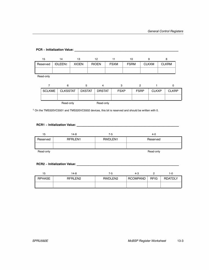
General Control Registers
13-3McBSP Register WorksheetSPRU592E
ÁÁÁÁÁÁÁÁÁÁÁÁÁÁÁÁÁÁÁÁÁÁÁÁÁÁÁÁÁÁÁÁÁÁÁÁÁÁÁÁÁÁÁÁÁÁÁÁÁÁÁÁÁÁÁÁÁÁÁÁ
PCR − Initialization Value: _____________________________________________________________ÁÁÁÁÁ
ÁÁÁÁÁÁÁÁÁÁÁÁÁÁÁÁÁÁÁÁÁÁÁÁÁÁÁÁÁÁÁÁÁÁÁÁÁÁÁÁÁÁÁÁÁÁÁÁÁÁÁÁÁÁÁÁÁÁÁ
ÁÁÁÁÁÁÁÁÁ
15ÁÁÁÁÁ
14ÁÁÁÁ
13ÁÁÁÁÁ
12ÁÁÁÁ
11ÁÁÁÁ
10ÁÁÁÁÁ
9ÁÁÁÁ
8ÁÁÁÁÁ
ÁReservedÎÎÎÎÎÎÎÎÎÎ
IDLEEN†ÎÎÎÎÎÎÎÎ
XIOENÎÎÎÎÎÎÎÎÎÎ
RIOENÎÎÎÎÎÎÎÎ
FSXMÎÎÎÎÎÎÎÎ
FSRMÎÎÎÎÎÎÎÎÎÎ
CLKXMÎÎÎÎÎÎÎÎ
CLKRMÁÁÁÁÁÁÁÁÁ
ÁÁ
ÎÎÎÎÎÎÎÎÎÎÎÎÎÎÎ
ÎÎÎÎÎÎÎÎÎÎÎÎ
ÎÎÎÎÎÎÎÎÎÎÎÎÎÎÎ
ÎÎÎÎÎÎÎÎÎÎÎÎ
ÎÎÎÎÎÎÎÎÎÎÎÎ
ÎÎÎÎÎÎÎÎÎÎÎÎÎÎÎ
ÎÎÎÎÎÎÎÎÎÎÎÎ
ÁÁÁÁÁÁ
ÁÁÁÁÁÁÁ
ÁÁÁÁÁÁÁÁÁ
Read-onlyÁÁÁÁÁÁÁÁÁÁ
ÁÁÁÁÁÁÁÁ
ÁÁÁÁÁÁÁÁÁÁ
ÁÁÁÁÁÁÁÁ
ÁÁÁÁÁÁÁÁ
ÁÁÁÁÁÁÁÁÁÁ
ÁÁÁÁÁÁÁÁ
ÁÁÁÁÁÁÁÁÁ
ÁÁÁÁÁÁÁÁÁ
ÁÁÁÁÁÁÁÁÁÁÁÁÁÁÁÁÁÁÁÁÁÁÁÁÁÁÁÁÁÁÁÁÁÁÁÁ
ÁÁÁÁÁÁÁÁÁÁ
ÁÁÁÁÁÁÁÁ
ÁÁÁÁÁÁÁÁÁÁÁÁÁÁÁ7 ÁÁÁÁÁ6 ÁÁÁÁÁ5 ÁÁÁÁ4 ÁÁÁÁÁ3 ÁÁÁÁ2 ÁÁÁÁ1 ÁÁÁÁ0 ÁÁÁ
ÁÁ
ÁÁÁÁÁÁ
SCLKME CLKSSTATÉÉÉÉÉÉÉÉÉÉÉÉÉÉÉ
DXSTATÉÉÉÉÉÉÉÉÉÉÉÉ
DRSTATÁÁÁÁÁÁÁÁÁÁÁÁÁÁÁ
FSXPÉÉÉÉÉÉÉÉÉÉÉÉ
FSRPÉÉÉÉÉÉÉÉÉÉÉÉ
CLKXPÁÁÁÁÁÁÁÁÁÁÁÁ
CLKRPÁÁÁÁÁÁÁ
ÁÁÁÁÁ
ÉÉÉÉÉÉÉÉÉÉ
ÉÉÉÉÉÉÉÉ
ÁÁÁÁÁÁÁÁÁÁ
ÉÉÉÉÉÉÉÉ
ÉÉÉÉÉÉÉÉ
ÁÁÁÁÁÁÁÁ
ÁÁÁÁÁ
ÁÁÁÁÁÁÁÁÁÁÁÁÁ
ÁÁÁÁÁÁÁÁÁÁ
Read-onlyÁÁÁÁÁÁÁÁÁÁ
ÁÁÁÁÁÁÁÁ
Read-onlyÁÁÁÁÁÁÁÁÁÁ
ÁÁÁÁÁÁÁÁ
ÁÁÁÁÁÁÁÁ
ÁÁÁÁÁÁÁÁ
ÁÁÁÁ† On the TMS320VC5501 and TMS320VC5502 devices, this bit is reserved and should be written with 0.
ÁÁÁÁÁÁÁÁÁÁÁÁÁÁÁÁÁÁÁÁÁÁÁÁÁÁÁÁÁÁÁÁÁÁÁÁÁÁÁÁÁÁÁÁÁÁÁÁÁÁÁÁÁÁÁÁÁÁÁÁ
RCR1 − Initialization Value: ____________________________________________________________ÁÁÁÁÁ
ÁÁÁÁÁÁÁÁÁÁÁÁÁÁÁÁÁÁÁÁÁÁÁÁÁÁÁÁÁÁÁÁÁÁÁÁÁÁÁÁÁÁÁÁÁÁÁÁÁÁÁÁÁÁÁÁÁÁÁ
ÁÁÁÁÁ
ÁÁÁÁÁÁÁÁÁÁÁ
15 ÁÁÁÁÁÁÁÁÁÁÁÁÁÁÁÁÁÁ
14-8 ÁÁÁÁÁÁÁÁÁÁÁÁÁÁ
7-5 ÁÁÁÁÁÁÁÁÁÁÁÁÁÁÁÁÁÁÁÁÁÁ
4-0 ÁÁÁÁÁ
ÁÎÎÎÎÎÎÎÎÎÎ
Reserved ÎÎÎÎÎÎÎÎÎÎÎÎÎÎÎÎÎÎ
RFRLEN1 ÎÎÎÎÎÎÎÎÎÎÎÎÎÎ
RWDLEN1 ÁÁÁÁÁÁÁÁÁÁÁÁÁÁÁÁÁÁÁÁÁÁ
Reserved ÁÁÁÁÁ
ÁÎÎÎÎÎÎÎÎÎÎ
ÎÎÎÎÎÎÎÎÎÎÎÎÎÎÎÎÎÎ
ÎÎÎÎÎÎÎÎÎÎÎÎÎÎ
ÁÁÁÁÁÁÁÁÁÁÁÁÁÁÁÁÁÁÁÁÁÁ
ÁÁÁÁÁ
ÁÁÁÁÁÁÁÁÁÁÁ
Read-only ÁÁÁÁÁÁÁÁÁÁÁÁÁÁÁÁÁÁ
ÁÁÁÁÁÁÁÁÁÁÁÁÁÁ
ÁÁÁÁÁÁÁÁÁÁÁÁÁÁÁÁÁÁÁÁÁÁ
Read-only ÁÁÁÁ
ÁÁÁÁÁÁÁÁÁÁÁÁÁÁÁÁÁÁÁÁÁÁÁÁÁÁÁÁÁÁÁÁÁÁÁÁÁÁÁÁÁÁÁÁÁÁÁÁÁÁÁÁÁÁÁÁÁÁÁÁRCR2 − Initialization Value: ____________________________________________________________
ÁÁÁÁÁ
ÁÁÁÁÁÁÁÁÁÁÁÁÁÁÁÁÁÁÁÁÁÁÁÁÁÁÁÁÁÁÁÁÁÁÁÁÁÁÁÁÁÁÁÁÁÁÁÁÁÁÁÁÁÁÁÁÁÁÁ
ÁÁÁÁÁ
ÁÁÁÁÁÁÁÁÁÁÁ
15ÁÁÁÁÁÁÁÁÁÁÁÁÁÁÁÁÁÁ
14-8ÁÁÁÁÁÁÁÁÁÁÁÁÁÁ
7-5ÁÁÁÁÁÁÁÁÁÁ
4-3ÁÁÁÁÁÁ
2ÁÁÁÁÁÁÁÁÁÁ
1-0ÁÁÁÁÁ
ÁRPHASE RFRLEN2 RWDLEN2 RCOMPAND RFIGÁÁÁÁÁ
ÁÁÁÁÁRDATDLYÁÁ
ÁÁÁÁ
ÁÁÁÁÁÁÁÁÁÁ
ÁÁÁÁÁ
ÁÁÁÁÁÁÁÁÁÁÁ
ÁÁÁÁÁÁÁÁÁÁÁÁÁÁÁÁÁÁ
ÁÁÁÁÁÁÁÁÁÁÁÁÁÁ
ÁÁÁÁÁÁÁÁÁÁ
ÁÁÁÁÁÁ
ÁÁÁÁÁÁÁÁÁÁ
ÁÁÁÁ

General Control Registers
McBSP Register Worksheet13-4 SPRU592E
ÁÁÁÁÁÁÁÁÁÁÁÁÁÁÁÁÁÁÁÁÁÁÁÁÁÁÁÁÁÁÁÁÁÁÁÁÁÁÁÁÁÁÁÁÁÁÁÁÁÁÁÁÁÁÁÁÁÁÁÁÁÁ
XCR1 − Initialization Value: ____________________________________________________________ ÁÁÁÁ
ÁÁÁÁÁÁÁÁÁÁÁÁÁÁÁÁÁÁÁÁÁÁÁÁÁÁÁÁÁÁÁÁÁÁÁÁÁÁÁÁÁÁÁÁÁÁÁÁÁÁÁÁÁÁÁÁÁÁÁÁ
ÁÁÁÁÁÁÁÁ15 ÁÁÁÁÁÁÁÁÁ14-8 ÁÁÁÁÁÁÁ7-5 ÁÁÁÁÁÁÁÁÁÁÁÁ4-0 ÁÁÁ
ÁÁÁÁ
ÎÎÎÎÎÎÎÎÎÎÎÎ
ReservedÎÎÎÎÎÎÎÎÎÎÎÎÎÎÎÎÎÎÎÎÎÎÎÎÎÎÎ
XFRLEN1ÎÎÎÎÎÎÎÎÎÎÎÎÎÎÎÎÎÎÎÎÎ
XWDLEN1ÁÁÁÁÁÁÁÁÁÁÁÁÁÁÁÁÁÁÁÁÁÁÁÁÁÁÁÁÁÁÁÁÁÁÁÁ
ReservedÁÁÁÁÁ
ÁÁÎÎÎÎÎÎÎÎ
ÎÎÎÎÎÎÎÎÎÎÎÎÎÎÎÎÎÎ
ÎÎÎÎÎÎÎÎÎÎÎÎÎÎ
ÁÁÁÁÁÁÁÁÁÁÁÁÁÁÁÁÁÁÁÁÁÁÁÁ
ÁÁÁÁ
ÁÁÁÁÁÁÁÁÁÁ
Read-onlyÁÁÁÁÁÁÁÁÁÁÁÁÁÁÁÁÁÁ
ÁÁÁÁÁÁÁÁÁÁÁÁÁÁ
ÁÁÁÁÁÁÁÁÁÁÁÁÁÁÁÁÁÁÁÁÁÁÁÁ
Read-only ÁÁ
ÁÁÁÁÁÁÁÁÁÁÁÁÁÁÁÁÁÁÁÁÁÁÁÁÁÁÁÁÁÁÁÁÁÁÁÁÁÁÁÁÁÁÁÁÁÁÁÁÁÁÁÁÁÁÁÁÁÁÁÁÁÁ
XCR2 − Initialization Value: ____________________________________________________________ÁÁÁÁ
ÁÁÁÁÁÁÁÁÁÁÁÁÁÁÁÁÁÁÁÁÁÁÁÁÁÁÁÁÁÁÁÁÁÁÁÁÁÁÁÁÁÁÁÁÁÁÁÁÁÁÁÁÁÁÁÁÁÁÁÁ
ÁÁÁÁ
ÁÁÁÁÁÁÁÁÁÁ
15 ÁÁÁÁÁÁÁÁÁÁÁÁÁÁÁÁÁÁ
14-8 ÁÁÁÁÁÁÁÁÁÁÁÁÁÁ
7-5 ÁÁÁÁÁÁÁÁÁÁ
4-3 ÁÁÁÁÁÁÁÁ
2 ÁÁÁÁÁÁÁÁÁÁ
1-0 ÁÁÁÁ
ÁÁXPHASE XFRLEN2 XWDLEN2 XCOMPAND XFIG ÁÁÁÁÁ
ÁÁÁÁÁXDATDLY Á
ÁÁÁÁÁ
ÁÁÁÁÁÁÁÁÁÁ
ÁÁÁÁ
ÁÁÁÁÁÁÁÁÁÁ
ÁÁÁÁÁÁÁÁÁÁÁÁÁÁÁÁÁÁ
ÁÁÁÁÁÁÁÁÁÁÁÁÁÁ
ÁÁÁÁÁÁÁÁÁÁ
ÁÁÁÁÁÁÁÁ
ÁÁÁÁÁÁÁÁÁÁ
ÁÁ
ÁÁÁÁÁÁÁÁÁÁÁÁÁÁÁÁÁÁÁÁÁÁÁÁÁÁÁÁÁÁÁÁÁÁÁÁÁÁÁÁÁÁÁÁÁÁÁÁÁÁÁÁÁÁÁÁÁÁÁÁÁÁ
SRGR1 − Initialization Value: ___________________________________________________________ÁÁÁÁ
ÁÁÁÁÁÁÁÁÁÁÁÁÁÁÁÁÁÁÁÁÁÁÁÁÁÁÁÁÁÁÁÁÁÁÁÁÁÁÁÁÁÁÁÁÁÁÁÁÁÁÁÁÁÁÁÁÁÁÁÁ
ÁÁÁÁÁÁÁÁÁÁÁÁÁÁÁÁÁÁÁ15-8 ÁÁÁÁÁÁÁÁÁÁÁÁÁÁÁ7-0 ÁÁÁ
ÁÁÁÁ
ÎÎÎÎÎÎÎÎÎÎÎÎÎÎÎÎÎÎÎÎÎÎÎÎÎÎÎÎÎÎÎÎÎÎÎÎÎÎÎÎÎÎÎÎÎ
FWIDÁÁÁÁÁÁÁÁÁÁÁÁÁÁÁÁÁÁÁÁÁÁÁÁÁÁÁÁÁÁÁÁÁÁÁÁÁÁÁÁÁÁÁÁÁ
CLKGDVÁÁÁÁÁ
ÁÁÎÎÎÎÎÎÎÎÎÎÎÎÎÎÎÎÎÎÎÎÎÎÎÎÎÎÎÎÎÎ
ÁÁÁÁÁÁÁÁÁÁÁÁÁÁÁÁÁÁÁÁÁÁÁÁÁÁÁÁÁÁ
ÁÁÁÁ
ÁÁÁÁÁÁÁÁÁÁÁÁÁÁÁÁÁÁÁÁÁÁÁÁÁÁÁÁÁÁÁÁ
ÁÁÁÁÁÁÁÁÁÁÁÁÁÁÁÁÁÁÁÁÁÁÁÁÁÁÁÁÁÁ
ÁÁ
ÁÁÁÁÁÁÁÁÁÁÁÁÁÁÁÁÁÁÁÁÁÁÁÁÁÁÁÁÁÁÁÁÁÁÁÁÁÁÁÁÁÁÁÁÁÁÁÁÁÁÁÁÁÁÁÁÁÁÁÁÁÁ
SRGR2 − Initialization Value: ___________________________________________________________ÁÁÁÁ
ÁÁÁÁÁÁÁÁÁÁÁÁÁÁÁÁÁÁÁÁÁÁÁÁÁÁÁÁÁÁÁÁÁÁÁÁÁÁÁÁÁÁÁÁÁÁÁÁÁÁÁÁÁÁÁÁÁÁÁÁ
ÁÁÁÁ
ÁÁÁÁÁÁÁÁÁÁ
15 ÁÁÁÁÁÁÁÁ
14 ÁÁÁÁÁÁÁÁ
13 ÁÁÁÁÁÁ
12ÁÁÁÁÁÁÁÁÁÁÁÁÁÁÁÁÁÁÁÁÁÁÁÁÁÁÁÁÁÁÁÁÁÁÁÁ
11-0 ÁÁÁÁ
ÁÁGSYNC† CLKSP CLKSM FSGMÁÁÁÁÁÁÁÁÁÁÁÁÁÁÁÁÁÁ
ÁÁÁÁÁÁÁÁÁÁÁÁÁÁÁÁÁÁFPER Á
ÁÁÁÁÁ
ÁÁÁÁÁÁÁÁÁÁÁÁÁÁÁÁÁÁÁÁÁÁÁÁÁÁÁÁÁÁÁÁÁÁÁÁ
ÁÁÁÁ
ÁÁÁÁÁÁÁÁÁÁ
ÁÁÁÁÁÁÁÁ
ÁÁÁÁÁÁÁÁ
ÁÁÁÁÁÁ
ÁÁÁÁÁÁÁÁÁÁÁÁÁÁÁÁÁÁÁÁÁÁÁÁÁÁÁÁÁÁÁÁÁÁÁÁ
ÁÁ
† On TMS320VC5501 and TMS320VC5502 devices, this bit is reserved and should be written with 0.

Multichannel Selection Control Registers
13-5McBSP Register WorksheetSPRU592E
13.2 Multichannel Selection Control Registers
ÁÁÁÁÁÁÁÁÁÁÁÁÁÁÁÁÁÁÁÁÁÁÁÁÁÁÁÁÁÁÁÁÁÁÁÁÁÁÁÁÁÁÁÁÁÁÁÁÁÁÁÁÁÁÁÁÁÁÁÁ
MCR1 − Initialization Value: ____________________________________________________________ÁÁÁÁÁ
ÁÁÁÁÁÁÁÁÁÁÁÁÁÁÁÁÁÁÁÁÁÁÁÁÁÁÁÁÁÁÁÁÁÁÁÁÁÁÁÁÁÁÁÁÁÁÁÁÁÁÁÁÁÁÁÁÁÁÁ
ÁÁÁÁÁ
ÁÁÁÁÁÁÁÁÁÁÁÁÁÁÁÁÁÁÁ
15-10 ÁÁÁÁÁÁÁÁ
9 ÁÁÁÁÁÁÁÁ
8-7 ÁÁÁÁÁÁÁÁ
6-5 ÁÁÁÁÁÁÁÁÁÁÁÁ
4-2 ÁÁÁÁÁÁÁÁ
1 ÁÁÁÁÁÁÁÁ
0 ÁÁÁÁÁ
ÁÎÎÎÎÎÎÎÎÎÎÎÎÎÎÎÎÎÎ
Reserved RMCME RPBBLK RPABLK RCBLK ReservedÁÁÁÁÁÁÁÁ
RMCMÁÁÁÁÁ
ÁÎÎÎÎÎÎÎÎÎÎÎÎÎÎÎÎÎÎ
ÁÁÁÁÁÁÁÁ
ÁÁÁÁÁ
ÁÁÁÁÁÁÁÁÁÁÁÁÁÁÁÁÁÁÁ
Read-only ÁÁÁÁÁÁÁÁ
ÁÁÁÁÁÁÁÁ
ÁÁÁÁÁÁÁÁ
ÁÁÁÁÁÁÁÁÁÁÁÁ
Read-only ÁÁÁÁÁÁÁÁ
Read-onlyÁÁÁÁÁÁÁÁ
ÁÁÁÁ
ÁÁÁÁÁÁÁÁÁÁÁÁÁÁÁÁÁÁÁÁÁÁÁÁÁÁÁÁÁÁÁÁÁÁÁÁÁÁÁÁÁÁÁÁÁÁÁÁÁÁÁÁÁÁÁÁÁÁÁÁMCR2 − Initialization Value: ____________________________________________________________
ÁÁÁÁÁ
ÁÁÁÁÁÁÁÁÁÁÁÁÁÁÁÁÁÁÁÁÁÁÁÁÁÁÁÁÁÁÁÁÁÁÁÁÁÁÁÁÁÁÁÁÁÁÁÁÁÁÁÁÁÁÁÁÁÁÁ
ÁÁÁÁÁ
ÁÁÁÁÁÁÁÁÁÁÁÁÁÁÁÁÁÁÁ
15-10ÁÁÁÁÁÁÁÁ
9ÁÁÁÁÁÁÁÁ
8-7ÁÁÁÁÁÁÁÁ
6-5ÁÁÁÁÁÁÁÁÁÁÁÁ
4-2ÁÁÁÁÁÁÁÁÁÁÁÁÁÁ
1-0ÁÁÁÁÁ
ÁÎÎÎÎÎÎÎÎÎÎÎÎÎÎÎÎÎÎ
Reserved XMCME XPBBLK XPABLK XCBLKÁÁÁÁÁÁÁÁÁÁÁÁÁÁ
XMCMÁÁÁÁÁ
ÁÁ
ÎÎÎÎÎÎÎÎÎÎÎÎÎÎÎÎÎÎÎÎÎÎÎÎÎÎÎ
ÁÁÁÁÁÁÁÁÁÁÁÁÁÁÁÁÁÁÁÁÁ
ÁÁÁÁÁÁÁ
ÁÁÁÁÁÁÁÁÁÁÁÁÁÁÁÁÁÁÁ
Read-only ÁÁÁÁÁÁÁÁ
ÁÁÁÁÁÁÁÁ
ÁÁÁÁÁÁÁÁ
ÁÁÁÁÁÁÁÁÁÁÁÁ
Read-only ÁÁÁÁÁÁÁÁÁÁÁÁÁÁ
ÁÁÁÁ
ÁÁÁÁÁÁÁÁÁÁÁÁÁÁÁÁÁÁÁÁÁÁÁÁÁÁÁÁÁÁÁÁÁÁÁÁÁÁÁÁÁÁÁÁÁÁÁÁÁÁÁÁÁÁÁÁÁÁÁÁ
RCERA − Initialization Value: ___________________________________________________________ÁÁÁÁÁ
ÁÁÁÁÁÁÁÁÁÁÁÁÁÁÁÁÁÁÁÁÁÁÁÁÁÁÁÁÁÁÁÁÁÁÁÁÁÁÁÁÁÁÁÁÁÁÁÁÁÁÁÁÁÁÁÁÁÁÁ
ÁÁÁÁÁ
ÁÁÁÁÁÁÁÁÁ
15 ÁÁÁÁÁÁÁÁÁÁ
14 ÁÁÁÁÁÁÁÁ
13 ÁÁÁÁÁÁÁÁÁÁ
12 ÁÁÁÁÁÁÁÁ
11 ÁÁÁÁÁÁÁÁ
10 ÁÁÁÁÁÁÁÁÁÁ
9 ÁÁÁÁÁÁÁÁ
8 ÁÁÁÁÁÁÁÁÁ
ÁRCE15ÎÎÎÎÎÎÎÎÎÎ
RCE14 ÎÎÎÎÎÎÎÎ
RCE13ÎÎÎÎÎÎÎÎÎÎ
RCE12 ÎÎÎÎÎÎÎÎ
RCE11 ÎÎÎÎÎÎÎÎ
RCE10ÎÎÎÎÎÎÎÎÎÎ
RCE9 ÎÎÎÎÎÎÎÎ
RCE8 ÁÁÁÁÁÁÁÁÁ
ÁÎÎÎÎÎÎÎÎÎÎ
ÎÎÎÎÎÎÎÎ
ÎÎÎÎÎÎÎÎÎÎ
ÎÎÎÎÎÎÎÎ
ÎÎÎÎÎÎÎÎ
ÎÎÎÎÎÎÎÎÎÎ
ÎÎÎÎÎÎÎÎ
ÁÁÁÁÁÁÁÁÁ
ÁÁ
ÁÁÁÁÁÁÁÁÁÁÁÁ
Channel_________
ÁÁÁÁÁÁÁÁÁÁÁÁÁÁÁ
Channel_________
ÁÁÁÁÁÁÁÁÁÁÁÁ
Channel_________
ÁÁÁÁÁÁÁÁÁÁÁÁÁÁÁ
Channel_________
ÁÁÁÁÁÁÁÁÁÁÁÁ
Channel_________
ÁÁÁÁÁÁÁÁÁÁÁÁ
Channel_________
ÁÁÁÁÁÁÁÁÁÁÁÁÁÁÁ
Channel_________
ÁÁÁÁÁÁÁÁÁÁÁÁ
Channel_________
ÁÁÁÁÁÁ
ÁÁÁÁÁÁÁ
ÁÁÁÁÁÁÁÁÁ
ÁÁÁÁÁÁÁÁÁÁ
ÁÁÁÁÁÁÁÁ
ÁÁÁÁÁÁÁÁÁÁ
ÁÁÁÁÁÁÁÁ
ÁÁÁÁÁÁÁÁ
ÁÁÁÁÁÁÁÁÁÁ
ÁÁÁÁÁÁÁÁ
ÁÁÁÁÁÁÁÁÁÁÁÁÁÁÁÁ7 ÁÁÁÁ6 ÁÁÁÁ5 ÁÁÁÁÁ4 ÁÁÁÁ3 ÁÁÁÁ2 ÁÁÁÁÁ1 ÁÁÁÁ0 ÁÁÁ
ÁÁ
ÁÁÁÁÁÁ
RCE7 RCE6ÉÉÉÉÉÉÉÉÉÉÉÉ
RCE5ÉÉÉÉÉÉÉÉÉÉÉÉÉÉÉ
RCE4ÁÁÁÁÁÁÁÁÁÁÁÁ
RCE3ÉÉÉÉÉÉÉÉÉÉÉÉ
RCE2ÉÉÉÉÉÉÉÉÉÉÉÉÉÉÉ
RCE1ÁÁÁÁÁÁÁÁÁÁÁÁ
RCE0ÁÁÁÁÁÁÁ
ÁÁÁÁÁ
ÉÉÉÉÉÉÉÉ
ÉÉÉÉÉÉÉÉÉÉ
ÁÁÁÁÁÁÁÁ
ÉÉÉÉÉÉÉÉ
ÉÉÉÉÉÉÉÉÉÉ
ÁÁÁÁÁÁÁÁ
ÁÁÁÁÁ
ÁÁÁÁÁÁÁÁÁÁÁÁÁÁÁ
Channel_________
ÁÁÁÁÁÁÁÁ
Channel_________
ÁÁÁÁÁÁÁÁ
Channel_________
ÁÁÁÁÁÁÁÁÁÁ
Channel_________
ÁÁÁÁÁÁÁÁ
Channel_________
ÁÁÁÁÁÁÁÁ
Channel_________
ÁÁÁÁÁÁÁÁÁÁ
Channel_________
ÁÁÁÁÁÁÁÁ
Channel_________
ÁÁÁÁ

Multichannel Selection Control Registers
McBSP Register Worksheet13-6 SPRU592E
ÁÁÁÁÁÁÁÁÁÁÁÁÁÁÁÁÁÁÁÁÁÁÁÁÁÁÁÁÁÁÁÁÁÁÁÁÁÁÁÁÁÁÁÁÁÁÁÁÁÁÁÁÁÁÁÁÁÁÁÁÁÁ
RCERB − Initialization Value: ___________________________________________________________ÁÁÁÁ
ÁÁÁÁÁÁÁÁÁÁÁÁÁÁÁÁÁÁÁÁÁÁÁÁÁÁÁÁÁÁÁÁÁÁÁÁÁÁÁÁÁÁÁÁÁÁÁÁÁÁÁÁÁÁÁÁÁÁÁÁ
ÁÁÁÁÁÁÁÁ
15ÁÁÁÁ
14ÁÁÁÁÁ
13ÁÁÁÁ
12ÁÁÁÁ
11ÁÁÁÁÁ
10ÁÁÁÁ
9ÁÁÁÁÁ
8ÁÁÁÁÁ
ÁÁRCE15
ÎÎÎÎÎÎÎÎ
RCE14ÎÎÎÎÎÎÎÎÎÎ
RCE13ÎÎÎÎÎÎÎÎ
RCE12ÎÎÎÎÎÎÎÎ
RCE11ÎÎÎÎÎÎÎÎÎÎ
RCE10ÎÎÎÎÎÎÎÎ
RCE9ÎÎÎÎÎÎÎÎÎÎ
RCE8ÁÁÁÁÁÁÁÁ
ÁÁÁÁ
ÎÎÎÎÎÎÎÎÎÎÎÎ
ÎÎÎÎÎÎÎÎÎÎÎÎÎÎÎ
ÎÎÎÎÎÎÎÎÎÎÎÎ
ÎÎÎÎÎÎÎÎÎÎÎÎ
ÎÎÎÎÎÎÎÎÎÎÎÎÎÎÎ
ÎÎÎÎÎÎÎÎÎÎÎÎ
ÎÎÎÎÎÎÎÎÎÎÎÎÎÎÎ
ÁÁÁÁÁÁ
ÁÁÁÁÁ
ÁÁÁÁÁÁÁÁÁÁ
Channel_________
ÁÁÁÁÁÁÁÁ
Channel_________
ÁÁÁÁÁÁÁÁÁÁ
Channel_________
ÁÁÁÁÁÁÁÁ
Channel_________
ÁÁÁÁÁÁÁÁ
Channel_________
ÁÁÁÁÁÁÁÁÁÁ
Channel_________
ÁÁÁÁÁÁÁÁ
Channel_________
ÁÁÁÁÁÁÁÁÁÁ
Channel_________
ÁÁÁÁÁÁÁÁ
ÁÁÁÁÁÁÁÁÁÁ
ÁÁÁÁÁÁÁÁ
ÁÁÁÁÁÁÁÁÁÁ
ÁÁÁÁÁÁÁÁ
ÁÁÁÁÁÁÁÁ
ÁÁÁÁÁÁÁÁÁÁ
ÁÁÁÁÁÁÁÁ
ÁÁÁÁÁÁÁÁÁÁ
ÁÁÁÁÁÁÁÁ
ÁÁÁÁÁÁÁÁÁÁÁÁÁÁ
7 ÁÁÁÁÁÁÁÁÁÁ
6 ÁÁÁÁÁÁÁÁ
5 ÁÁÁÁÁÁÁÁ
4 ÁÁÁÁÁÁÁÁÁÁ
3 ÁÁÁÁÁÁÁÁ
2 ÁÁÁÁÁÁÁÁ
1 ÁÁÁÁÁÁÁÁÁÁ
0 ÁÁÁÁ
ÁÁÁÁÁÁ
RCE7 RCE6 ÉÉÉÉÉÉÉÉ
RCE5 ÉÉÉÉÉÉÉÉ
RCE4ÁÁÁÁÁÁÁÁÁÁ
RCE3 ÉÉÉÉÉÉÉÉ
RCE2 ÉÉÉÉÉÉÉÉ
RCE1ÁÁÁÁÁÁÁÁÁÁ
RCE0 ÁÁÁÁ
ÁÁÁÁÁÁ
ÉÉÉÉÉÉÉÉ
ÉÉÉÉÉÉÉÉ
ÁÁÁÁÁÁÁÁÁÁ
ÉÉÉÉÉÉÉÉ
ÉÉÉÉÉÉÉÉ
ÁÁÁÁÁÁÁÁÁÁ
ÁÁÁÁ
ÁÁÁÁ
ÁÁÁÁÁÁ
ÁÁÁÁÁÁÁÁÁÁÁÁ
Channel_________
ÁÁÁÁÁÁÁÁÁÁÁÁÁÁÁ
Channel_________
ÁÁÁÁÁÁÁÁÁÁÁÁ
Channel_________
ÁÁÁÁÁÁÁÁÁÁÁÁ
Channel_________
ÁÁÁÁÁÁÁÁÁÁÁÁÁÁÁ
Channel_________
ÁÁÁÁÁÁÁÁÁÁÁÁ
Channel_________
ÁÁÁÁÁÁÁÁÁÁÁÁ
Channel_________
ÁÁÁÁÁÁÁÁÁÁÁÁÁÁÁ
Channel_________
ÁÁÁ
ÁÁÁÁÁÁÁÁÁÁÁÁÁÁÁÁÁÁÁÁÁÁÁÁÁÁÁÁÁÁÁÁÁÁÁÁÁÁÁÁÁÁÁÁÁÁÁÁÁÁÁÁÁÁÁÁÁÁÁÁÁÁRCERC − Initialization Value: ___________________________________________________________
ÁÁÁÁ
ÁÁÁÁÁÁÁÁÁÁÁÁÁÁÁÁÁÁÁÁÁÁÁÁÁÁÁÁÁÁÁÁÁÁÁÁÁÁÁÁÁÁÁÁÁÁÁÁÁÁÁÁÁÁÁÁÁÁÁÁ
ÁÁÁÁ
ÁÁÁÁÁÁÁÁÁÁ
15ÁÁÁÁÁÁÁÁ
14ÁÁÁÁÁÁÁÁÁÁ
13ÁÁÁÁÁÁÁÁ
12ÁÁÁÁÁÁÁÁ
11ÁÁÁÁÁÁÁÁÁÁ
10ÁÁÁÁÁÁÁÁ
9ÁÁÁÁÁÁÁÁÁÁ
8ÁÁÁÁÁÁÁÁ
ÁÁRCE15
ÎÎÎÎÎÎÎÎ
RCE14ÎÎÎÎÎÎÎÎÎÎ
RCE13ÎÎÎÎÎÎÎÎ
RCE12ÎÎÎÎÎÎÎÎ
RCE11ÎÎÎÎÎÎÎÎÎÎ
RCE10ÎÎÎÎÎÎÎÎ
RCE9ÎÎÎÎÎÎÎÎÎÎ
RCE8ÁÁÁÁÁÁÁÁ
ÁÁÎÎÎÎÎÎÎÎ
ÎÎÎÎÎÎÎÎÎÎ
ÎÎÎÎÎÎÎÎ
ÎÎÎÎÎÎÎÎ
ÎÎÎÎÎÎÎÎÎÎ
ÎÎÎÎÎÎÎÎ
ÎÎÎÎÎÎÎÎÎÎ
ÁÁÁÁÁÁÁÁ
ÁÁÁÁ
ÁÁÁÁÁÁÁÁÁÁÁÁ
Channel47
ÁÁÁÁÁÁÁÁÁÁÁÁ
Channel46
ÁÁÁÁÁÁÁÁÁÁÁÁÁÁÁ
Channel45
ÁÁÁÁÁÁÁÁÁÁÁÁ
Channel44
ÁÁÁÁÁÁÁÁÁÁÁÁ
Channel43
ÁÁÁÁÁÁÁÁÁÁÁÁÁÁÁ
Channel42
ÁÁÁÁÁÁÁÁÁÁÁÁ
Channel41
ÁÁÁÁÁÁÁÁÁÁÁÁÁÁÁ
Channel40
ÁÁÁÁÁÁ
ÁÁÁÁÁ
ÁÁÁÁÁÁÁÁÁÁ
ÁÁÁÁÁÁÁÁ
ÁÁÁÁÁÁÁÁÁÁ
ÁÁÁÁÁÁÁÁ
ÁÁÁÁÁÁÁÁ
ÁÁÁÁÁÁÁÁÁÁ
ÁÁÁÁÁÁÁÁ
ÁÁÁÁÁÁÁÁÁÁ
ÁÁÁÁÁÁÁÁ
ÁÁÁÁÁÁÁÁÁÁÁÁÁÁ
7 ÁÁÁÁÁÁÁÁÁÁ
6 ÁÁÁÁÁÁÁÁ
5 ÁÁÁÁÁÁÁÁ
4 ÁÁÁÁÁÁÁÁÁÁ
3 ÁÁÁÁÁÁÁÁ
2 ÁÁÁÁÁÁÁÁ
1 ÁÁÁÁÁÁÁÁÁÁ
0 ÁÁÁÁ
ÁÁÁÁÁÁ
RCE7 RCE6 ÉÉÉÉÉÉÉÉ
RCE5 ÉÉÉÉÉÉÉÉ
RCE4ÁÁÁÁÁÁÁÁÁÁ
RCE3 ÉÉÉÉÉÉÉÉ
RCE2 ÉÉÉÉÉÉÉÉ
RCE1ÁÁÁÁÁÁÁÁÁÁ
RCE0 ÁÁÁÁ
ÁÁÁÁÁÁ
ÉÉÉÉÉÉÉÉ
ÉÉÉÉÉÉÉÉ
ÁÁÁÁÁÁÁÁÁÁ
ÉÉÉÉÉÉÉÉ
ÉÉÉÉÉÉÉÉ
ÁÁÁÁÁÁÁÁÁÁ
ÁÁÁÁ
ÁÁÁÁ
ÁÁÁÁÁÁ
ÁÁÁÁÁÁÁÁÁÁÁÁ
Channel39
ÁÁÁÁÁÁÁÁÁÁÁÁÁÁÁ
Channel38
ÁÁÁÁÁÁÁÁÁÁÁÁ
Channel37
ÁÁÁÁÁÁÁÁÁÁÁÁ
Channel36
ÁÁÁÁÁÁÁÁÁÁÁÁÁÁÁ
Channel35
ÁÁÁÁÁÁÁÁÁÁÁÁ
Channel34
ÁÁÁÁÁÁÁÁÁÁÁÁ
Channel33
ÁÁÁÁÁÁÁÁÁÁÁÁÁÁÁ
Channel32
ÁÁÁ

Multichannel Selection Control Registers
13-7McBSP Register WorksheetSPRU592E
ÁÁÁÁÁÁÁÁÁÁÁÁÁÁÁÁÁÁÁÁÁÁÁÁÁÁÁÁÁÁÁÁÁÁÁÁÁÁÁÁÁÁÁÁÁÁÁÁÁÁÁÁÁÁÁÁÁÁÁÁ
RCERD − Initialization Value: ___________________________________________________________ÁÁÁÁÁ
ÁÁÁÁÁÁÁÁÁÁÁÁÁÁÁÁÁÁÁÁÁÁÁÁÁÁÁÁÁÁÁÁÁÁÁÁÁÁÁÁÁÁÁÁÁÁÁÁÁÁÁÁÁÁÁÁÁÁÁ
ÁÁÁÁÁÁÁÁÁ
15ÁÁÁÁÁ
14ÁÁÁÁ
13ÁÁÁÁÁ
12ÁÁÁÁ
11ÁÁÁÁ
10ÁÁÁÁÁ
9ÁÁÁÁ
8ÁÁÁÁÁ
ÁRCE15ÎÎÎÎÎÎÎÎÎÎ
RCE14ÎÎÎÎÎÎÎÎ
RCE13ÎÎÎÎÎÎÎÎÎÎ
RCE12ÎÎÎÎÎÎÎÎ
RCE11ÎÎÎÎÎÎÎÎ
RCE10ÎÎÎÎÎÎÎÎÎÎ
RCE9ÎÎÎÎÎÎÎÎ
RCE8ÁÁÁÁÁÁÁÁÁ
ÁÁ
ÎÎÎÎÎÎÎÎÎÎÎÎÎÎÎ
ÎÎÎÎÎÎÎÎÎÎÎÎ
ÎÎÎÎÎÎÎÎÎÎÎÎÎÎÎ
ÎÎÎÎÎÎÎÎÎÎÎÎ
ÎÎÎÎÎÎÎÎÎÎÎÎ
ÎÎÎÎÎÎÎÎÎÎÎÎÎÎÎ
ÎÎÎÎÎÎÎÎÎÎÎÎ
ÁÁÁÁÁÁ
ÁÁÁÁÁÁÁ
ÁÁÁÁÁÁÁÁÁ
Channel63ÁÁÁÁÁÁÁÁÁÁ
Channel62ÁÁÁÁÁÁÁÁ
Channel61ÁÁÁÁÁÁÁÁÁÁ
Channel60ÁÁÁÁÁÁÁÁ
Channel59ÁÁÁÁÁÁÁÁ
Channel58ÁÁÁÁÁÁÁÁÁÁ
Channel57ÁÁÁÁÁÁÁÁ
Channel56ÁÁÁÁÁÁÁÁÁ
ÁÁÁÁÁÁÁÁÁ
ÁÁÁÁÁÁÁÁÁÁ
ÁÁÁÁÁÁÁÁ
ÁÁÁÁÁÁÁÁÁÁ
ÁÁÁÁÁÁÁÁ
ÁÁÁÁÁÁÁÁ
ÁÁÁÁÁÁÁÁÁÁ
ÁÁÁÁÁÁÁÁ
ÁÁÁÁÁÁÁÁÁ
ÁÁÁÁÁÁÁÁÁÁÁÁÁÁÁ
7 ÁÁÁÁÁÁÁÁ
6 ÁÁÁÁÁÁÁÁ
5 ÁÁÁÁÁÁÁÁÁÁ
4 ÁÁÁÁÁÁÁÁ
3 ÁÁÁÁÁÁÁÁ
2 ÁÁÁÁÁÁÁÁÁÁ
1 ÁÁÁÁÁÁÁÁ
0 ÁÁÁÁÁ
ÁÁÁÁÁ
RCE7 RCE6 ÉÉÉÉÉÉÉÉ
RCE5ÉÉÉÉÉÉÉÉÉÉ
RCE4 ÁÁÁÁÁÁÁÁ
RCE3 ÉÉÉÉÉÉÉÉ
RCE2ÉÉÉÉÉÉÉÉÉÉ
RCE1 ÁÁÁÁÁÁÁÁ
RCE0 ÁÁÁÁÁ
ÁÁÁÁÁ
ÉÉÉÉÉÉÉÉ
ÉÉÉÉÉÉÉÉÉÉ
ÁÁÁÁÁÁÁÁ
ÉÉÉÉÉÉÉÉ
ÉÉÉÉÉÉÉÉÉÉ
ÁÁÁÁÁÁÁÁ
ÁÁÁÁÁ
ÁÁ
ÁÁÁÁÁÁ
ÁÁÁÁÁÁÁÁÁÁÁÁÁÁÁ
Channel55
ÁÁÁÁÁÁÁÁÁÁÁÁ
Channel54
ÁÁÁÁÁÁÁÁÁÁÁÁ
Channel53
ÁÁÁÁÁÁÁÁÁÁÁÁÁÁÁ
Channel52
ÁÁÁÁÁÁÁÁÁÁÁÁ
Channel51
ÁÁÁÁÁÁÁÁÁÁÁÁ
Channel50
ÁÁÁÁÁÁÁÁÁÁÁÁÁÁÁ
Channel49
ÁÁÁÁÁÁÁÁÁÁÁÁ
Channel48
ÁÁÁÁÁÁ
ÁÁÁÁÁÁÁÁÁÁÁÁÁÁÁÁÁÁÁÁÁÁÁÁÁÁÁÁÁÁÁÁÁÁÁÁÁÁÁÁÁÁÁÁÁÁÁÁÁÁÁÁÁÁÁÁÁÁÁÁRCERE − Initialization Value: ___________________________________________________________
ÁÁÁÁÁ
ÁÁÁÁÁÁÁÁÁÁÁÁÁÁÁÁÁÁÁÁÁÁÁÁÁÁÁÁÁÁÁÁÁÁÁÁÁÁÁÁÁÁÁÁÁÁÁÁÁÁÁÁÁÁÁÁÁÁÁ
ÁÁÁÁÁ
ÁÁÁÁÁÁÁÁÁ
15ÁÁÁÁÁÁÁÁÁÁ
14ÁÁÁÁÁÁÁÁ
13ÁÁÁÁÁÁÁÁÁÁ
12ÁÁÁÁÁÁÁÁ
11ÁÁÁÁÁÁÁÁ
10ÁÁÁÁÁÁÁÁÁÁ
9ÁÁÁÁÁÁÁÁ
8ÁÁÁÁÁÁÁÁÁ
ÁRCE15ÎÎÎÎÎÎÎÎÎÎ
RCE14ÎÎÎÎÎÎÎÎ
RCE13ÎÎÎÎÎÎÎÎÎÎ
RCE12ÎÎÎÎÎÎÎÎ
RCE11ÎÎÎÎÎÎÎÎ
RCE10ÎÎÎÎÎÎÎÎÎÎ
RCE9ÎÎÎÎÎÎÎÎ
RCE8ÁÁÁÁÁÁÁÁÁ
ÁÎÎÎÎÎÎÎÎÎÎ
ÎÎÎÎÎÎÎÎ
ÎÎÎÎÎÎÎÎÎÎ
ÎÎÎÎÎÎÎÎ
ÎÎÎÎÎÎÎÎ
ÎÎÎÎÎÎÎÎÎÎ
ÎÎÎÎÎÎÎÎ
ÁÁÁÁÁÁÁÁÁ
ÁÁ
ÁÁÁÁÁÁÁÁÁÁÁÁ
Channel79
ÁÁÁÁÁÁÁÁÁÁÁÁÁÁÁ
Channel78
ÁÁÁÁÁÁÁÁÁÁÁÁ
Channel77
ÁÁÁÁÁÁÁÁÁÁÁÁÁÁÁ
Channel76
ÁÁÁÁÁÁÁÁÁÁÁÁ
Channel75
ÁÁÁÁÁÁÁÁÁÁÁÁ
Channel74
ÁÁÁÁÁÁÁÁÁÁÁÁÁÁÁ
Channel73
ÁÁÁÁÁÁÁÁÁÁÁÁ
Channel72
ÁÁÁÁÁÁ
ÁÁÁÁÁÁÁ
ÁÁÁÁÁÁÁÁÁ
ÁÁÁÁÁÁÁÁÁÁ
ÁÁÁÁÁÁÁÁ
ÁÁÁÁÁÁÁÁÁÁ
ÁÁÁÁÁÁÁÁ
ÁÁÁÁÁÁÁÁ
ÁÁÁÁÁÁÁÁÁÁ
ÁÁÁÁÁÁÁÁ
ÁÁÁÁÁÁÁÁÁ
ÁÁÁÁÁÁÁÁÁÁÁÁÁÁÁ
7 ÁÁÁÁÁÁÁÁ
6 ÁÁÁÁÁÁÁÁ
5 ÁÁÁÁÁÁÁÁÁÁ
4 ÁÁÁÁÁÁÁÁ
3 ÁÁÁÁÁÁÁÁ
2 ÁÁÁÁÁÁÁÁÁÁ
1 ÁÁÁÁÁÁÁÁ
0 ÁÁÁÁÁ
ÁÁÁÁÁ
RCE7 RCE6 ÉÉÉÉÉÉÉÉ
RCE5ÉÉÉÉÉÉÉÉÉÉ
RCE4 ÁÁÁÁÁÁÁÁ
RCE3 ÉÉÉÉÉÉÉÉ
RCE2ÉÉÉÉÉÉÉÉÉÉ
RCE1 ÁÁÁÁÁÁÁÁ
RCE0 ÁÁÁÁÁ
ÁÁÁÁÁ
ÉÉÉÉÉÉÉÉ
ÉÉÉÉÉÉÉÉÉÉ
ÁÁÁÁÁÁÁÁ
ÉÉÉÉÉÉÉÉ
ÉÉÉÉÉÉÉÉÉÉ
ÁÁÁÁÁÁÁÁ
ÁÁÁÁÁ
ÁÁ
ÁÁÁÁÁÁ
ÁÁÁÁÁÁÁÁÁÁÁÁÁÁÁ
Channel71
ÁÁÁÁÁÁÁÁÁÁÁÁ
Channel70
ÁÁÁÁÁÁÁÁÁÁÁÁ
Channel69
ÁÁÁÁÁÁÁÁÁÁÁÁÁÁÁ
Channel68
ÁÁÁÁÁÁÁÁÁÁÁÁ
Channel67
ÁÁÁÁÁÁÁÁÁÁÁÁ
Channel66
ÁÁÁÁÁÁÁÁÁÁÁÁÁÁÁ
Channel65
ÁÁÁÁÁÁÁÁÁÁÁÁ
Channel64
ÁÁÁÁÁÁ

Multichannel Selection Control Registers
McBSP Register Worksheet13-8 SPRU592E
ÁÁÁÁÁÁÁÁÁÁÁÁÁÁÁÁÁÁÁÁÁÁÁÁÁÁÁÁÁÁÁÁÁÁÁÁÁÁÁÁÁÁÁÁÁÁÁÁÁÁÁÁÁÁÁÁÁÁÁÁÁÁ
RCERF − Initialization Value: ___________________________________________________________ÁÁÁÁ
ÁÁÁÁÁÁÁÁÁÁÁÁÁÁÁÁÁÁÁÁÁÁÁÁÁÁÁÁÁÁÁÁÁÁÁÁÁÁÁÁÁÁÁÁÁÁÁÁÁÁÁÁÁÁÁÁÁÁÁÁ
ÁÁÁÁÁÁÁÁ
15ÁÁÁÁ
14ÁÁÁÁÁ
13ÁÁÁÁ
12ÁÁÁÁ
11ÁÁÁÁÁ
10ÁÁÁÁ
9ÁÁÁÁÁ
8ÁÁÁÁÁ
ÁÁRCE15
ÎÎÎÎÎÎÎÎ
RCE14ÎÎÎÎÎÎÎÎÎÎ
RCE13ÎÎÎÎÎÎÎÎ
RCE12ÎÎÎÎÎÎÎÎ
RCE11ÎÎÎÎÎÎÎÎÎÎ
RCE10ÎÎÎÎÎÎÎÎ
RCE9ÎÎÎÎÎÎÎÎÎÎ
RCE8ÁÁÁÁÁÁÁÁ
ÁÁÁÁ
ÎÎÎÎÎÎÎÎÎÎÎÎ
ÎÎÎÎÎÎÎÎÎÎÎÎÎÎÎ
ÎÎÎÎÎÎÎÎÎÎÎÎ
ÎÎÎÎÎÎÎÎÎÎÎÎ
ÎÎÎÎÎÎÎÎÎÎÎÎÎÎÎ
ÎÎÎÎÎÎÎÎÎÎÎÎ
ÎÎÎÎÎÎÎÎÎÎÎÎÎÎÎ
ÁÁÁÁÁÁ
ÁÁÁÁÁ
ÁÁÁÁÁÁÁÁÁÁ
Channel95ÁÁÁÁÁÁÁÁ
Channel94ÁÁÁÁÁÁÁÁÁÁ
Channel93ÁÁÁÁÁÁÁÁ
Channel92ÁÁÁÁÁÁÁÁ
Channel91ÁÁÁÁÁÁÁÁÁÁ
Channel90ÁÁÁÁÁÁÁÁ
Channel89ÁÁÁÁÁÁÁÁÁÁ
Channel88ÁÁÁÁÁÁÁÁ
ÁÁÁÁÁÁÁÁÁÁ
ÁÁÁÁÁÁÁÁ
ÁÁÁÁÁÁÁÁÁÁ
ÁÁÁÁÁÁÁÁ
ÁÁÁÁÁÁÁÁ
ÁÁÁÁÁÁÁÁÁÁ
ÁÁÁÁÁÁÁÁ
ÁÁÁÁÁÁÁÁÁÁ
ÁÁÁÁÁÁÁÁ
ÁÁÁÁÁÁÁÁÁÁÁÁÁÁ
7 ÁÁÁÁÁÁÁÁÁÁ
6 ÁÁÁÁÁÁÁÁ
5 ÁÁÁÁÁÁÁÁ
4 ÁÁÁÁÁÁÁÁÁÁ
3 ÁÁÁÁÁÁÁÁ
2 ÁÁÁÁÁÁÁÁ
1 ÁÁÁÁÁÁÁÁÁÁ
0 ÁÁÁÁ
ÁÁÁÁÁÁ
RCE7 RCE6 ÉÉÉÉÉÉÉÉ
RCE5 ÉÉÉÉÉÉÉÉ
RCE4ÁÁÁÁÁÁÁÁÁÁ
RCE3 ÉÉÉÉÉÉÉÉ
RCE2 ÉÉÉÉÉÉÉÉ
RCE1ÁÁÁÁÁÁÁÁÁÁ
RCE0 ÁÁÁÁ
ÁÁÁÁÁÁ
ÉÉÉÉÉÉÉÉ
ÉÉÉÉÉÉÉÉ
ÁÁÁÁÁÁÁÁÁÁ
ÉÉÉÉÉÉÉÉ
ÉÉÉÉÉÉÉÉ
ÁÁÁÁÁÁÁÁÁÁ
ÁÁÁÁ
ÁÁÁÁ
ÁÁÁÁÁÁ
ÁÁÁÁÁÁÁÁÁÁÁÁ
Channel87
ÁÁÁÁÁÁÁÁÁÁÁÁÁÁÁ
Channel86
ÁÁÁÁÁÁÁÁÁÁÁÁ
Channel85
ÁÁÁÁÁÁÁÁÁÁÁÁ
Channel84
ÁÁÁÁÁÁÁÁÁÁÁÁÁÁÁ
Channel83
ÁÁÁÁÁÁÁÁÁÁÁÁ
Channel82
ÁÁÁÁÁÁÁÁÁÁÁÁ
Channel81
ÁÁÁÁÁÁÁÁÁÁÁÁÁÁÁ
Channel80
ÁÁÁ
ÁÁÁÁÁÁÁÁÁÁÁÁÁÁÁÁÁÁÁÁÁÁÁÁÁÁÁÁÁÁÁÁÁÁÁÁÁÁÁÁÁÁÁÁÁÁÁÁÁÁÁÁÁÁÁÁÁÁÁÁÁÁRCERG − Initialization Value: ___________________________________________________________
ÁÁÁÁ
ÁÁÁÁÁÁÁÁÁÁÁÁÁÁÁÁÁÁÁÁÁÁÁÁÁÁÁÁÁÁÁÁÁÁÁÁÁÁÁÁÁÁÁÁÁÁÁÁÁÁÁÁÁÁÁÁÁÁÁÁ
ÁÁÁÁ
ÁÁÁÁÁÁÁÁÁÁ
15ÁÁÁÁÁÁÁÁ
14ÁÁÁÁÁÁÁÁÁÁ
13ÁÁÁÁÁÁÁÁ
12ÁÁÁÁÁÁÁÁ
11ÁÁÁÁÁÁÁÁÁÁ
10ÁÁÁÁÁÁÁÁ
9ÁÁÁÁÁÁÁÁÁÁ
8ÁÁÁÁÁÁÁÁ
ÁÁRCE15
ÎÎÎÎÎÎÎÎ
RCE14ÎÎÎÎÎÎÎÎÎÎ
RCE13ÎÎÎÎÎÎÎÎ
RCE12ÎÎÎÎÎÎÎÎ
RCE11ÎÎÎÎÎÎÎÎÎÎ
RCE10ÎÎÎÎÎÎÎÎ
RCE9ÎÎÎÎÎÎÎÎÎÎ
RCE8ÁÁÁÁÁÁÁÁ
ÁÁÎÎÎÎÎÎÎÎ
ÎÎÎÎÎÎÎÎÎÎ
ÎÎÎÎÎÎÎÎ
ÎÎÎÎÎÎÎÎ
ÎÎÎÎÎÎÎÎÎÎ
ÎÎÎÎÎÎÎÎ
ÎÎÎÎÎÎÎÎÎÎ
ÁÁÁÁÁÁÁÁ
ÁÁÁÁ
ÁÁÁÁÁÁÁÁÁÁÁÁ
Channel111
ÁÁÁÁÁÁÁÁÁÁÁÁ
Channel110
ÁÁÁÁÁÁÁÁÁÁÁÁÁÁÁ
Channel109
ÁÁÁÁÁÁÁÁÁÁÁÁ
Channel108
ÁÁÁÁÁÁÁÁÁÁÁÁ
Channel107
ÁÁÁÁÁÁÁÁÁÁÁÁÁÁÁ
Channel106
ÁÁÁÁÁÁÁÁÁÁÁÁ
Channel105
ÁÁÁÁÁÁÁÁÁÁÁÁÁÁÁ
Channel104
ÁÁÁÁÁÁ
ÁÁÁÁÁ
ÁÁÁÁÁÁÁÁÁÁ
ÁÁÁÁÁÁÁÁ
ÁÁÁÁÁÁÁÁÁÁ
ÁÁÁÁÁÁÁÁ
ÁÁÁÁÁÁÁÁ
ÁÁÁÁÁÁÁÁÁÁ
ÁÁÁÁÁÁÁÁ
ÁÁÁÁÁÁÁÁÁÁ
ÁÁÁÁÁÁÁÁ
ÁÁÁÁÁÁÁÁÁÁÁÁÁÁ
7 ÁÁÁÁÁÁÁÁÁÁ
6 ÁÁÁÁÁÁÁÁ
5 ÁÁÁÁÁÁÁÁ
4 ÁÁÁÁÁÁÁÁÁÁ
3 ÁÁÁÁÁÁÁÁ
2 ÁÁÁÁÁÁÁÁ
1 ÁÁÁÁÁÁÁÁÁÁ
0 ÁÁÁÁ
ÁÁÁÁÁÁ
RCE7 RCE6 ÉÉÉÉÉÉÉÉ
RCE5 ÉÉÉÉÉÉÉÉ
RCE4ÁÁÁÁÁÁÁÁÁÁ
RCE3 ÉÉÉÉÉÉÉÉ
RCE2 ÉÉÉÉÉÉÉÉ
RCE1ÁÁÁÁÁÁÁÁÁÁ
RCE0 ÁÁÁÁ
ÁÁÁÁÁÁ
ÉÉÉÉÉÉÉÉ
ÉÉÉÉÉÉÉÉ
ÁÁÁÁÁÁÁÁÁÁ
ÉÉÉÉÉÉÉÉ
ÉÉÉÉÉÉÉÉ
ÁÁÁÁÁÁÁÁÁÁ
ÁÁÁÁ
ÁÁÁÁ
ÁÁÁÁÁÁ
ÁÁÁÁÁÁÁÁÁÁÁÁ
Channel103
ÁÁÁÁÁÁÁÁÁÁÁÁÁÁÁ
Channel102
ÁÁÁÁÁÁÁÁÁÁÁÁ
Channel101
ÁÁÁÁÁÁÁÁÁÁÁÁ
Channel100
ÁÁÁÁÁÁÁÁÁÁÁÁÁÁÁ
Channel99
ÁÁÁÁÁÁÁÁÁÁÁÁ
Channel98
ÁÁÁÁÁÁÁÁÁÁÁÁ
Channel97
ÁÁÁÁÁÁÁÁÁÁÁÁÁÁÁ
Channel96
ÁÁÁ

Multichannel Selection Control Registers
13-9McBSP Register WorksheetSPRU592E
ÁÁÁÁÁÁÁÁÁÁÁÁÁÁÁÁÁÁÁÁÁÁÁÁÁÁÁÁÁÁÁÁÁÁÁÁÁÁÁÁÁÁÁÁÁÁÁÁÁÁÁÁÁÁÁÁÁÁÁÁ
RCERH − Initialization Value: ___________________________________________________________ÁÁÁÁÁ
ÁÁÁÁÁÁÁÁÁÁÁÁÁÁÁÁÁÁÁÁÁÁÁÁÁÁÁÁÁÁÁÁÁÁÁÁÁÁÁÁÁÁÁÁÁÁÁÁÁÁÁÁÁÁÁÁÁÁÁ
ÁÁÁÁÁÁÁÁÁ
15ÁÁÁÁÁ
14ÁÁÁÁ
13ÁÁÁÁÁ
12ÁÁÁÁ
11ÁÁÁÁ
10ÁÁÁÁÁ
9ÁÁÁÁ
8ÁÁÁÁÁ
ÁRCE15ÎÎÎÎÎÎÎÎÎÎ
RCE14ÎÎÎÎÎÎÎÎ
RCE13ÎÎÎÎÎÎÎÎÎÎ
RCE12ÎÎÎÎÎÎÎÎ
RCE11ÎÎÎÎÎÎÎÎ
RCE10ÎÎÎÎÎÎÎÎÎÎ
RCE9ÎÎÎÎÎÎÎÎ
RCE8ÁÁÁÁÁÁÁÁÁ
ÁÁ
ÎÎÎÎÎÎÎÎÎÎÎÎÎÎÎ
ÎÎÎÎÎÎÎÎÎÎÎÎ
ÎÎÎÎÎÎÎÎÎÎÎÎÎÎÎ
ÎÎÎÎÎÎÎÎÎÎÎÎ
ÎÎÎÎÎÎÎÎÎÎÎÎ
ÎÎÎÎÎÎÎÎÎÎÎÎÎÎÎ
ÎÎÎÎÎÎÎÎÎÎÎÎ
ÁÁÁÁÁÁ
ÁÁÁÁÁÁÁ
ÁÁÁÁÁÁÁÁÁ
Channel127ÁÁÁÁÁÁÁÁÁÁ
Channel126ÁÁÁÁÁÁÁÁ
Channel125ÁÁÁÁÁÁÁÁÁÁ
Channel124
ÁÁÁÁÁÁÁÁ
Channel123ÁÁÁÁÁÁÁÁ
Channel122ÁÁÁÁÁÁÁÁÁÁ
Channel121
ÁÁÁÁÁÁÁÁ
Channel120ÁÁÁÁÁÁÁÁÁ
ÁÁÁÁÁÁÁÁÁ
ÁÁÁÁÁÁÁÁÁÁ
ÁÁÁÁÁÁÁÁ
ÁÁÁÁÁÁÁÁÁÁ
ÁÁÁÁÁÁÁÁ
ÁÁÁÁÁÁÁÁ
ÁÁÁÁÁÁÁÁÁÁ
ÁÁÁÁÁÁÁÁ
ÁÁÁÁÁÁÁÁÁ
ÁÁÁÁÁÁÁÁÁÁÁÁÁÁÁ
7 ÁÁÁÁÁÁÁÁ
6 ÁÁÁÁÁÁÁÁ
5 ÁÁÁÁÁÁÁÁÁÁ
4 ÁÁÁÁÁÁÁÁ
3 ÁÁÁÁÁÁÁÁ
2 ÁÁÁÁÁÁÁÁÁÁ
1 ÁÁÁÁÁÁÁÁ
0 ÁÁÁÁÁ
ÁÁÁÁÁ
RCE7 RCE6 ÉÉÉÉÉÉÉÉ
RCE5ÉÉÉÉÉÉÉÉÉÉ
RCE4 ÁÁÁÁÁÁÁÁ
RCE3 ÉÉÉÉÉÉÉÉ
RCE2ÉÉÉÉÉÉÉÉÉÉ
RCE1 ÁÁÁÁÁÁÁÁ
RCE0 ÁÁÁÁÁ
ÁÁÁÁÁ
ÉÉÉÉÉÉÉÉ
ÉÉÉÉÉÉÉÉÉÉ
ÁÁÁÁÁÁÁÁ
ÉÉÉÉÉÉÉÉ
ÉÉÉÉÉÉÉÉÉÉ
ÁÁÁÁÁÁÁÁ
ÁÁÁÁÁ
ÁÁ
ÁÁÁÁÁÁ
ÁÁÁÁÁÁÁÁÁÁÁÁÁÁÁ
Channel119
ÁÁÁÁÁÁÁÁÁÁÁÁ
Channel118
ÁÁÁÁÁÁÁÁÁÁÁÁ
Channel117
ÁÁÁÁÁÁÁÁÁÁÁÁÁÁÁ
Channel116
ÁÁÁÁÁÁÁÁÁÁÁÁ
Channel115
ÁÁÁÁÁÁÁÁÁÁÁÁ
Channel114
ÁÁÁÁÁÁÁÁÁÁÁÁÁÁÁ
Channel113
ÁÁÁÁÁÁÁÁÁÁÁÁ
Channel112
ÁÁÁÁÁÁ
ÁÁÁÁÁÁÁÁÁÁÁÁÁÁÁÁÁÁÁÁÁÁÁÁÁÁÁÁÁÁÁÁÁÁÁÁÁÁÁÁÁÁÁÁÁÁÁÁÁÁÁÁÁÁÁÁÁÁÁÁXCERA − Initialization Value: ___________________________________________________________
ÁÁÁÁÁ
ÁÁÁÁÁÁÁÁÁÁÁÁÁÁÁÁÁÁÁÁÁÁÁÁÁÁÁÁÁÁÁÁÁÁÁÁÁÁÁÁÁÁÁÁÁÁÁÁÁÁÁÁÁÁÁÁÁÁÁ
ÁÁÁÁÁ
ÁÁÁÁÁÁÁÁÁ
15ÁÁÁÁÁÁÁÁÁÁ
14ÁÁÁÁÁÁÁÁ
13ÁÁÁÁÁÁÁÁÁÁ
12ÁÁÁÁÁÁÁÁ
11ÁÁÁÁÁÁÁÁ
10ÁÁÁÁÁÁÁÁÁÁ
9ÁÁÁÁÁÁÁÁ
8ÁÁÁÁÁÁÁÁÁ
ÁXCE15ÎÎÎÎÎÎÎÎÎÎ
XCE14ÎÎÎÎÎÎÎÎ
XCE13ÎÎÎÎÎÎÎÎÎÎ
XCE12ÎÎÎÎÎÎÎÎ
XCE11ÎÎÎÎÎÎÎÎ
XCE10ÎÎÎÎÎÎÎÎÎÎ
XCE9ÎÎÎÎÎÎÎÎ
XCE8ÁÁÁÁÁÁÁÁÁ
ÁÎÎÎÎÎÎÎÎÎÎ
ÎÎÎÎÎÎÎÎ
ÎÎÎÎÎÎÎÎÎÎ
ÎÎÎÎÎÎÎÎ
ÎÎÎÎÎÎÎÎ
ÎÎÎÎÎÎÎÎÎÎ
ÎÎÎÎÎÎÎÎ
ÁÁÁÁÁÁÁÁÁ
ÁÁ
ÁÁÁÁÁÁÁÁÁÁÁÁ
Channel_________
ÁÁÁÁÁÁÁÁÁÁÁÁÁÁÁ
Channel_________
ÁÁÁÁÁÁÁÁÁÁÁÁ
Channel_________
ÁÁÁÁÁÁÁÁÁÁÁÁÁÁÁ
Channel_________
ÁÁÁÁÁÁÁÁÁÁÁÁ
Channel_________
ÁÁÁÁÁÁÁÁÁÁÁÁ
Channel_________
ÁÁÁÁÁÁÁÁÁÁÁÁÁÁÁ
Channel_________
ÁÁÁÁÁÁÁÁÁÁÁÁ
Channel_________
ÁÁÁÁÁÁ
ÁÁÁÁÁÁÁ
ÁÁÁÁÁÁÁÁÁ
ÁÁÁÁÁÁÁÁÁÁ
ÁÁÁÁÁÁÁÁ
ÁÁÁÁÁÁÁÁÁÁ
ÁÁÁÁÁÁÁÁ
ÁÁÁÁÁÁÁÁ
ÁÁÁÁÁÁÁÁÁÁ
ÁÁÁÁÁÁÁÁ
ÁÁÁÁÁÁÁÁÁ
ÁÁÁÁÁÁÁÁÁÁÁÁÁÁÁ
7 ÁÁÁÁÁÁÁÁ
6 ÁÁÁÁÁÁÁÁ
5 ÁÁÁÁÁÁÁÁÁÁ
4 ÁÁÁÁÁÁÁÁ
3 ÁÁÁÁÁÁÁÁ
2 ÁÁÁÁÁÁÁÁÁÁ
1 ÁÁÁÁÁÁÁÁ
0 ÁÁÁÁÁ
ÁÁÁÁÁ
XCE7 XCE6 ÉÉÉÉÉÉÉÉ
XCE5ÉÉÉÉÉÉÉÉÉÉ
XCE4 ÁÁÁÁÁÁÁÁ
XCE3 ÉÉÉÉÉÉÉÉ
XCE2ÉÉÉÉÉÉÉÉÉÉ
XCE1 ÁÁÁÁÁÁÁÁ
XCE0 ÁÁÁÁÁ
ÁÁÁÁÁ
ÉÉÉÉÉÉÉÉ
ÉÉÉÉÉÉÉÉÉÉ
ÁÁÁÁÁÁÁÁ
ÉÉÉÉÉÉÉÉ
ÉÉÉÉÉÉÉÉÉÉ
ÁÁÁÁÁÁÁÁ
ÁÁÁÁÁ
ÁÁ
ÁÁÁÁÁÁ
ÁÁÁÁÁÁÁÁÁÁÁÁÁÁÁ
Channel_________
ÁÁÁÁÁÁÁÁÁÁÁÁ
Channel_________
ÁÁÁÁÁÁÁÁÁÁÁÁ
Channel_________
ÁÁÁÁÁÁÁÁÁÁÁÁÁÁÁ
Channel_________
ÁÁÁÁÁÁÁÁÁÁÁÁ
Channel_________
ÁÁÁÁÁÁÁÁÁÁÁÁ
Channel_________
ÁÁÁÁÁÁÁÁÁÁÁÁÁÁÁ
Channel_________
ÁÁÁÁÁÁÁÁÁÁÁÁ
Channel_________
ÁÁÁÁÁÁ
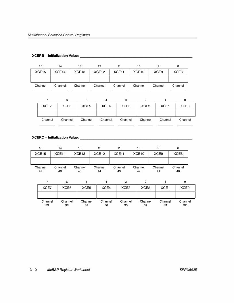
Multichannel Selection Control Registers
McBSP Register Worksheet13-10 SPRU592E
ÁÁÁÁÁÁÁÁÁÁÁÁÁÁÁÁÁÁÁÁÁÁÁÁÁÁÁÁÁÁÁÁÁÁÁÁÁÁÁÁÁÁÁÁÁÁÁÁÁÁÁÁÁÁÁÁÁÁÁÁÁÁ
XCERB − Initialization Value: ___________________________________________________________ÁÁÁÁ
ÁÁÁÁÁÁÁÁÁÁÁÁÁÁÁÁÁÁÁÁÁÁÁÁÁÁÁÁÁÁÁÁÁÁÁÁÁÁÁÁÁÁÁÁÁÁÁÁÁÁÁÁÁÁÁÁÁÁÁÁ
ÁÁÁÁÁÁÁÁ
15ÁÁÁÁ
14ÁÁÁÁÁ
13ÁÁÁÁ
12ÁÁÁÁ
11ÁÁÁÁÁ
10ÁÁÁÁ
9ÁÁÁÁÁ
8ÁÁÁÁÁ
ÁÁXCE15
ÎÎÎÎÎÎÎÎ
XCE14ÎÎÎÎÎÎÎÎÎÎ
XCE13ÎÎÎÎÎÎÎÎ
XCE12ÎÎÎÎÎÎÎÎ
XCE11ÎÎÎÎÎÎÎÎÎÎ
XCE10ÎÎÎÎÎÎÎÎ
XCE9ÎÎÎÎÎÎÎÎÎÎ
XCE8ÁÁÁÁÁÁÁÁ
ÁÁÁÁ
ÎÎÎÎÎÎÎÎÎÎÎÎ
ÎÎÎÎÎÎÎÎÎÎÎÎÎÎÎ
ÎÎÎÎÎÎÎÎÎÎÎÎ
ÎÎÎÎÎÎÎÎÎÎÎÎ
ÎÎÎÎÎÎÎÎÎÎÎÎÎÎÎ
ÎÎÎÎÎÎÎÎÎÎÎÎ
ÎÎÎÎÎÎÎÎÎÎÎÎÎÎÎ
ÁÁÁÁÁÁ
ÁÁÁÁÁ
ÁÁÁÁÁÁÁÁÁÁ
Channel_________
ÁÁÁÁÁÁÁÁ
Channel_________
ÁÁÁÁÁÁÁÁÁÁ
Channel_________
ÁÁÁÁÁÁÁÁ
Channel_________
ÁÁÁÁÁÁÁÁ
Channel_________
ÁÁÁÁÁÁÁÁÁÁ
Channel_________
ÁÁÁÁÁÁÁÁ
Channel_________
ÁÁÁÁÁÁÁÁÁÁ
Channel_________
ÁÁÁÁÁÁÁÁ
ÁÁÁÁÁÁÁÁÁÁ
ÁÁÁÁÁÁÁÁ
ÁÁÁÁÁÁÁÁÁÁ
ÁÁÁÁÁÁÁÁ
ÁÁÁÁÁÁÁÁ
ÁÁÁÁÁÁÁÁÁÁ
ÁÁÁÁÁÁÁÁ
ÁÁÁÁÁÁÁÁÁÁ
ÁÁÁÁÁÁÁÁ
ÁÁÁÁÁÁÁÁÁÁÁÁÁÁ
7 ÁÁÁÁÁÁÁÁÁÁ
6 ÁÁÁÁÁÁÁÁ
5 ÁÁÁÁÁÁÁÁ
4 ÁÁÁÁÁÁÁÁÁÁ
3 ÁÁÁÁÁÁÁÁ
2 ÁÁÁÁÁÁÁÁ
1 ÁÁÁÁÁÁÁÁÁÁ
0 ÁÁÁÁ
ÁÁÁÁÁÁ
XCE7 XCE6 ÉÉÉÉÉÉÉÉ
XCE5 ÉÉÉÉÉÉÉÉ
XCE4ÁÁÁÁÁÁÁÁÁÁ
XCE3 ÉÉÉÉÉÉÉÉ
XCE2 ÉÉÉÉÉÉÉÉ
XCE1ÁÁÁÁÁÁÁÁÁÁ
XCE0 ÁÁÁÁ
ÁÁÁÁÁÁ
ÉÉÉÉÉÉÉÉ
ÉÉÉÉÉÉÉÉ
ÁÁÁÁÁÁÁÁÁÁ
ÉÉÉÉÉÉÉÉ
ÉÉÉÉÉÉÉÉ
ÁÁÁÁÁÁÁÁÁÁ
ÁÁÁÁ
ÁÁÁÁ
ÁÁÁÁÁÁ
ÁÁÁÁÁÁÁÁÁÁÁÁ
Channel_________
ÁÁÁÁÁÁÁÁÁÁÁÁÁÁÁ
Channel_________
ÁÁÁÁÁÁÁÁÁÁÁÁ
Channel_________
ÁÁÁÁÁÁÁÁÁÁÁÁ
Channel_________
ÁÁÁÁÁÁÁÁÁÁÁÁÁÁÁ
Channel_________
ÁÁÁÁÁÁÁÁÁÁÁÁ
Channel_________
ÁÁÁÁÁÁÁÁÁÁÁÁ
Channel_________
ÁÁÁÁÁÁÁÁÁÁÁÁÁÁÁ
Channel_________
ÁÁÁ
ÁÁÁÁÁÁÁÁÁÁÁÁÁÁÁÁÁÁÁÁÁÁÁÁÁÁÁÁÁÁÁÁÁÁÁÁÁÁÁÁÁÁÁÁÁÁÁÁÁÁÁÁÁÁÁÁÁÁÁÁÁÁXCERC − Initialization Value: ___________________________________________________________
ÁÁÁÁ
ÁÁÁÁÁÁÁÁÁÁÁÁÁÁÁÁÁÁÁÁÁÁÁÁÁÁÁÁÁÁÁÁÁÁÁÁÁÁÁÁÁÁÁÁÁÁÁÁÁÁÁÁÁÁÁÁÁÁÁÁ
ÁÁÁÁ
ÁÁÁÁÁÁÁÁÁÁ
15ÁÁÁÁÁÁÁÁ
14ÁÁÁÁÁÁÁÁÁÁ
13ÁÁÁÁÁÁÁÁ
12ÁÁÁÁÁÁÁÁ
11ÁÁÁÁÁÁÁÁÁÁ
10ÁÁÁÁÁÁÁÁ
9ÁÁÁÁÁÁÁÁÁÁ
8ÁÁÁÁÁÁÁÁ
ÁÁXCE15
ÎÎÎÎÎÎÎÎ
XCE14ÎÎÎÎÎÎÎÎÎÎ
XCE13ÎÎÎÎÎÎÎÎ
XCE12ÎÎÎÎÎÎÎÎ
XCE11ÎÎÎÎÎÎÎÎÎÎ
XCE10ÎÎÎÎÎÎÎÎ
XCE9ÎÎÎÎÎÎÎÎÎÎ
XCE8ÁÁÁÁÁÁÁÁ
ÁÁÎÎÎÎÎÎÎÎ
ÎÎÎÎÎÎÎÎÎÎ
ÎÎÎÎÎÎÎÎ
ÎÎÎÎÎÎÎÎ
ÎÎÎÎÎÎÎÎÎÎ
ÎÎÎÎÎÎÎÎ
ÎÎÎÎÎÎÎÎÎÎ
ÁÁÁÁÁÁÁÁ
ÁÁÁÁ
ÁÁÁÁÁÁÁÁÁÁÁÁ
Channel47
ÁÁÁÁÁÁÁÁÁÁÁÁ
Channel46
ÁÁÁÁÁÁÁÁÁÁÁÁÁÁÁ
Channel45
ÁÁÁÁÁÁÁÁÁÁÁÁ
Channel44
ÁÁÁÁÁÁÁÁÁÁÁÁ
Channel43
ÁÁÁÁÁÁÁÁÁÁÁÁÁÁÁ
Channel42
ÁÁÁÁÁÁÁÁÁÁÁÁ
Channel41
ÁÁÁÁÁÁÁÁÁÁÁÁÁÁÁ
Channel40
ÁÁÁÁÁÁ
ÁÁÁÁÁ
ÁÁÁÁÁÁÁÁÁÁ
ÁÁÁÁÁÁÁÁ
ÁÁÁÁÁÁÁÁÁÁ
ÁÁÁÁÁÁÁÁ
ÁÁÁÁÁÁÁÁ
ÁÁÁÁÁÁÁÁÁÁ
ÁÁÁÁÁÁÁÁ
ÁÁÁÁÁÁÁÁÁÁ
ÁÁÁÁÁÁÁÁ
ÁÁÁÁÁÁÁÁÁÁÁÁÁÁ
7 ÁÁÁÁÁÁÁÁÁÁ
6 ÁÁÁÁÁÁÁÁ
5 ÁÁÁÁÁÁÁÁ
4 ÁÁÁÁÁÁÁÁÁÁ
3 ÁÁÁÁÁÁÁÁ
2 ÁÁÁÁÁÁÁÁ
1 ÁÁÁÁÁÁÁÁÁÁ
0 ÁÁÁÁ
ÁÁÁÁÁÁ
XCE7 XCE6 ÉÉÉÉÉÉÉÉ
XCE5 ÉÉÉÉÉÉÉÉ
XCE4ÁÁÁÁÁÁÁÁÁÁ
XCE3 ÉÉÉÉÉÉÉÉ
XCE2 ÉÉÉÉÉÉÉÉ
XCE1ÁÁÁÁÁÁÁÁÁÁ
XCE0 ÁÁÁÁ
ÁÁÁÁÁÁ
ÉÉÉÉÉÉÉÉ
ÉÉÉÉÉÉÉÉ
ÁÁÁÁÁÁÁÁÁÁ
ÉÉÉÉÉÉÉÉ
ÉÉÉÉÉÉÉÉ
ÁÁÁÁÁÁÁÁÁÁ
ÁÁÁÁ
ÁÁÁÁ
ÁÁÁÁÁÁ
ÁÁÁÁÁÁÁÁÁÁÁÁ
Channel39
ÁÁÁÁÁÁÁÁÁÁÁÁÁÁÁ
Channel38
ÁÁÁÁÁÁÁÁÁÁÁÁ
Channel37
ÁÁÁÁÁÁÁÁÁÁÁÁ
Channel36
ÁÁÁÁÁÁÁÁÁÁÁÁÁÁÁ
Channel35
ÁÁÁÁÁÁÁÁÁÁÁÁ
Channel34
ÁÁÁÁÁÁÁÁÁÁÁÁ
Channel33
ÁÁÁÁÁÁÁÁÁÁÁÁÁÁÁ
Channel32
ÁÁÁ

Multichannel Selection Control Registers
13-11McBSP Register WorksheetSPRU592E
ÁÁÁÁÁÁÁÁÁÁÁÁÁÁÁÁÁÁÁÁÁÁÁÁÁÁÁÁÁÁÁÁÁÁÁÁÁÁÁÁÁÁÁÁÁÁÁÁÁÁÁÁÁÁÁÁÁÁÁÁ
XCERD − Initialization Value: ___________________________________________________________ÁÁÁÁÁ
ÁÁÁÁÁÁÁÁÁÁÁÁÁÁÁÁÁÁÁÁÁÁÁÁÁÁÁÁÁÁÁÁÁÁÁÁÁÁÁÁÁÁÁÁÁÁÁÁÁÁÁÁÁÁÁÁÁÁÁ
ÁÁÁÁÁÁÁÁÁ
15ÁÁÁÁÁ
14ÁÁÁÁ
13ÁÁÁÁÁ
12ÁÁÁÁ
11ÁÁÁÁ
10ÁÁÁÁÁ
9ÁÁÁÁ
8ÁÁÁÁÁ
ÁXCE15ÎÎÎÎÎÎÎÎÎÎ
XCE14ÎÎÎÎÎÎÎÎ
XCE13ÎÎÎÎÎÎÎÎÎÎ
XCE12ÎÎÎÎÎÎÎÎ
XCE11ÎÎÎÎÎÎÎÎ
XCE10ÎÎÎÎÎÎÎÎÎÎ
XCE9ÎÎÎÎÎÎÎÎ
XCE8ÁÁÁÁÁÁÁÁÁ
ÁÁ
ÎÎÎÎÎÎÎÎÎÎÎÎÎÎÎ
ÎÎÎÎÎÎÎÎÎÎÎÎ
ÎÎÎÎÎÎÎÎÎÎÎÎÎÎÎ
ÎÎÎÎÎÎÎÎÎÎÎÎ
ÎÎÎÎÎÎÎÎÎÎÎÎ
ÎÎÎÎÎÎÎÎÎÎÎÎÎÎÎ
ÎÎÎÎÎÎÎÎÎÎÎÎ
ÁÁÁÁÁÁ
ÁÁÁÁÁÁÁ
ÁÁÁÁÁÁÁÁÁ
Channel63ÁÁÁÁÁÁÁÁÁÁ
Channel62ÁÁÁÁÁÁÁÁ
Channel61ÁÁÁÁÁÁÁÁÁÁ
Channel60ÁÁÁÁÁÁÁÁ
Channel59ÁÁÁÁÁÁÁÁ
Channel58ÁÁÁÁÁÁÁÁÁÁ
Channel57ÁÁÁÁÁÁÁÁ
Channel56ÁÁÁÁÁÁÁÁÁ
ÁÁÁÁÁÁÁÁÁ
ÁÁÁÁÁÁÁÁÁÁ
ÁÁÁÁÁÁÁÁ
ÁÁÁÁÁÁÁÁÁÁ
ÁÁÁÁÁÁÁÁ
ÁÁÁÁÁÁÁÁ
ÁÁÁÁÁÁÁÁÁÁ
ÁÁÁÁÁÁÁÁ
ÁÁÁÁÁÁÁÁÁ
ÁÁÁÁÁÁÁÁÁÁÁÁÁÁÁ
7 ÁÁÁÁÁÁÁÁ
6 ÁÁÁÁÁÁÁÁ
5 ÁÁÁÁÁÁÁÁÁÁ
4 ÁÁÁÁÁÁÁÁ
3 ÁÁÁÁÁÁÁÁ
2 ÁÁÁÁÁÁÁÁÁÁ
1 ÁÁÁÁÁÁÁÁ
0 ÁÁÁÁÁ
ÁÁÁÁÁ
XCE7 XCE6 ÉÉÉÉÉÉÉÉ
XCE5ÉÉÉÉÉÉÉÉÉÉ
XCE4 ÁÁÁÁÁÁÁÁ
XCE3 ÉÉÉÉÉÉÉÉ
XCE2ÉÉÉÉÉÉÉÉÉÉ
XCE1 ÁÁÁÁÁÁÁÁ
XCE0 ÁÁÁÁÁ
ÁÁÁÁÁ
ÉÉÉÉÉÉÉÉ
ÉÉÉÉÉÉÉÉÉÉ
ÁÁÁÁÁÁÁÁ
ÉÉÉÉÉÉÉÉ
ÉÉÉÉÉÉÉÉÉÉ
ÁÁÁÁÁÁÁÁ
ÁÁÁÁÁ
ÁÁ
ÁÁÁÁÁÁ
ÁÁÁÁÁÁÁÁÁÁÁÁÁÁÁ
Channel55
ÁÁÁÁÁÁÁÁÁÁÁÁ
Channel54
ÁÁÁÁÁÁÁÁÁÁÁÁ
Channel53
ÁÁÁÁÁÁÁÁÁÁÁÁÁÁÁ
Channel52
ÁÁÁÁÁÁÁÁÁÁÁÁ
Channel51
ÁÁÁÁÁÁÁÁÁÁÁÁ
Channel50
ÁÁÁÁÁÁÁÁÁÁÁÁÁÁÁ
Channel49
ÁÁÁÁÁÁÁÁÁÁÁÁ
Channel48
ÁÁÁÁÁÁ
ÁÁÁÁÁÁÁÁÁÁÁÁÁÁÁÁÁÁÁÁÁÁÁÁÁÁÁÁÁÁÁÁÁÁÁÁÁÁÁÁÁÁÁÁÁÁÁÁÁÁÁÁÁÁÁÁÁÁÁÁXCERE − Initialization Value: ___________________________________________________________
ÁÁÁÁÁ
ÁÁÁÁÁÁÁÁÁÁÁÁÁÁÁÁÁÁÁÁÁÁÁÁÁÁÁÁÁÁÁÁÁÁÁÁÁÁÁÁÁÁÁÁÁÁÁÁÁÁÁÁÁÁÁÁÁÁÁ
ÁÁÁÁÁ
ÁÁÁÁÁÁÁÁÁ
15ÁÁÁÁÁÁÁÁÁÁ
14ÁÁÁÁÁÁÁÁ
13ÁÁÁÁÁÁÁÁÁÁ
12ÁÁÁÁÁÁÁÁ
11ÁÁÁÁÁÁÁÁ
10ÁÁÁÁÁÁÁÁÁÁ
9ÁÁÁÁÁÁÁÁ
8ÁÁÁÁÁÁÁÁÁ
ÁXCE15ÎÎÎÎÎÎÎÎÎÎ
XCE14ÎÎÎÎÎÎÎÎ
XCE13ÎÎÎÎÎÎÎÎÎÎ
XCE12ÎÎÎÎÎÎÎÎ
XCE11ÎÎÎÎÎÎÎÎ
XCE10ÎÎÎÎÎÎÎÎÎÎ
XCE9ÎÎÎÎÎÎÎÎ
XCE8ÁÁÁÁÁÁÁÁÁ
ÁÎÎÎÎÎÎÎÎÎÎ
ÎÎÎÎÎÎÎÎ
ÎÎÎÎÎÎÎÎÎÎ
ÎÎÎÎÎÎÎÎ
ÎÎÎÎÎÎÎÎ
ÎÎÎÎÎÎÎÎÎÎ
ÎÎÎÎÎÎÎÎ
ÁÁÁÁÁÁÁÁÁ
ÁÁ
ÁÁÁÁÁÁÁÁÁÁÁÁ
Channel79
ÁÁÁÁÁÁÁÁÁÁÁÁÁÁÁ
Channel78
ÁÁÁÁÁÁÁÁÁÁÁÁ
Channel77
ÁÁÁÁÁÁÁÁÁÁÁÁÁÁÁ
Channel76
ÁÁÁÁÁÁÁÁÁÁÁÁ
Channel75
ÁÁÁÁÁÁÁÁÁÁÁÁ
Channel74
ÁÁÁÁÁÁÁÁÁÁÁÁÁÁÁ
Channel73
ÁÁÁÁÁÁÁÁÁÁÁÁ
Channel72
ÁÁÁÁÁÁ
ÁÁÁÁÁÁÁ
ÁÁÁÁÁÁÁÁÁ
ÁÁÁÁÁÁÁÁÁÁ
ÁÁÁÁÁÁÁÁ
ÁÁÁÁÁÁÁÁÁÁ
ÁÁÁÁÁÁÁÁ
ÁÁÁÁÁÁÁÁ
ÁÁÁÁÁÁÁÁÁÁ
ÁÁÁÁÁÁÁÁ
ÁÁÁÁÁÁÁÁÁ
ÁÁÁÁÁÁÁÁÁÁÁÁÁÁÁ
7 ÁÁÁÁÁÁÁÁ
6 ÁÁÁÁÁÁÁÁ
5 ÁÁÁÁÁÁÁÁÁÁ
4 ÁÁÁÁÁÁÁÁ
3 ÁÁÁÁÁÁÁÁ
2 ÁÁÁÁÁÁÁÁÁÁ
1 ÁÁÁÁÁÁÁÁ
0 ÁÁÁÁÁ
ÁÁÁÁÁ
XCE7 XCE6 ÉÉÉÉÉÉÉÉ
XCE5ÉÉÉÉÉÉÉÉÉÉ
XCE4 ÁÁÁÁÁÁÁÁ
XCE3 ÉÉÉÉÉÉÉÉ
XCE2ÉÉÉÉÉÉÉÉÉÉ
XCE1 ÁÁÁÁÁÁÁÁ
XCE0 ÁÁÁÁÁ
ÁÁÁÁÁ
ÉÉÉÉÉÉÉÉ
ÉÉÉÉÉÉÉÉÉÉ
ÁÁÁÁÁÁÁÁ
ÉÉÉÉÉÉÉÉ
ÉÉÉÉÉÉÉÉÉÉ
ÁÁÁÁÁÁÁÁ
ÁÁÁÁÁ
ÁÁ
ÁÁÁÁÁÁ
ÁÁÁÁÁÁÁÁÁÁÁÁÁÁÁ
Channel71
ÁÁÁÁÁÁÁÁÁÁÁÁ
Channel70
ÁÁÁÁÁÁÁÁÁÁÁÁ
Channel69
ÁÁÁÁÁÁÁÁÁÁÁÁÁÁÁ
Channel68
ÁÁÁÁÁÁÁÁÁÁÁÁ
Channel67
ÁÁÁÁÁÁÁÁÁÁÁÁ
Channel66
ÁÁÁÁÁÁÁÁÁÁÁÁÁÁÁ
Channel65
ÁÁÁÁÁÁÁÁÁÁÁÁ
Channel64
ÁÁÁÁÁÁ

Multichannel Selection Control Registers
McBSP Register Worksheet13-12 SPRU592E
ÁÁÁÁÁÁÁÁÁÁÁÁÁÁÁÁÁÁÁÁÁÁÁÁÁÁÁÁÁÁÁÁÁÁÁÁÁÁÁÁÁÁÁÁÁÁÁÁÁÁÁÁÁÁÁÁÁÁÁÁÁÁ
XCERF − Initialization Value: ___________________________________________________________ ÁÁÁÁ
ÁÁÁÁÁÁÁÁÁÁÁÁÁÁÁÁÁÁÁÁÁÁÁÁÁÁÁÁÁÁÁÁÁÁÁÁÁÁÁÁÁÁÁÁÁÁÁÁÁÁÁÁÁÁÁÁÁÁÁÁ
ÁÁÁÁÁÁÁÁ
15ÁÁÁÁ
14ÁÁÁÁÁ
13ÁÁÁÁ
12ÁÁÁÁ
11ÁÁÁÁÁ
10ÁÁÁÁ
9ÁÁÁÁÁ
8ÁÁÁÁÁ
ÁÁXCE15
ÎÎÎÎÎÎÎÎ
XCE14ÎÎÎÎÎÎÎÎÎÎ
XCE13ÎÎÎÎÎÎÎÎ
XCE12ÎÎÎÎÎÎÎÎ
XCE11ÎÎÎÎÎÎÎÎÎÎ
XCE10ÎÎÎÎÎÎÎÎ
XCE9ÎÎÎÎÎÎÎÎÎÎ
XCE8ÁÁÁÁÁÁÁÁ
ÁÁÁÁ
ÎÎÎÎÎÎÎÎÎÎÎÎ
ÎÎÎÎÎÎÎÎÎÎÎÎÎÎÎ
ÎÎÎÎÎÎÎÎÎÎÎÎ
ÎÎÎÎÎÎÎÎÎÎÎÎ
ÎÎÎÎÎÎÎÎÎÎÎÎÎÎÎ
ÎÎÎÎÎÎÎÎÎÎÎÎ
ÎÎÎÎÎÎÎÎÎÎÎÎÎÎÎ
ÁÁÁÁÁÁ
ÁÁÁÁÁ
ÁÁÁÁÁÁÁÁÁÁ
Channel95ÁÁÁÁÁÁÁÁ
Channel94ÁÁÁÁÁÁÁÁÁÁ
Channel93ÁÁÁÁÁÁÁÁ
Channel92ÁÁÁÁÁÁÁÁ
Channel91ÁÁÁÁÁÁÁÁÁÁ
Channel90ÁÁÁÁÁÁÁÁ
Channel89ÁÁÁÁÁÁÁÁÁÁ
Channel88ÁÁÁÁÁÁÁÁ
ÁÁÁÁÁÁÁÁÁÁ
ÁÁÁÁÁÁÁÁ
ÁÁÁÁÁÁÁÁÁÁ
ÁÁÁÁÁÁÁÁ
ÁÁÁÁÁÁÁÁ
ÁÁÁÁÁÁÁÁÁÁ
ÁÁÁÁÁÁÁÁ
ÁÁÁÁÁÁÁÁÁÁ
ÁÁÁÁÁÁÁÁ
ÁÁÁÁÁÁÁÁÁÁÁÁÁÁ
7 ÁÁÁÁÁÁÁÁÁÁ
6 ÁÁÁÁÁÁÁÁ
5 ÁÁÁÁÁÁÁÁ
4 ÁÁÁÁÁÁÁÁÁÁ
3 ÁÁÁÁÁÁÁÁ
2 ÁÁÁÁÁÁÁÁ
1 ÁÁÁÁÁÁÁÁÁÁ
0 ÁÁÁÁ
ÁÁÁÁÁÁ
XCE7 XCE6 ÉÉÉÉÉÉÉÉ
XCE5 ÉÉÉÉÉÉÉÉ
XCE4ÁÁÁÁÁÁÁÁÁÁ
XCE3 ÉÉÉÉÉÉÉÉ
XCE2 ÉÉÉÉÉÉÉÉ
XCE1ÁÁÁÁÁÁÁÁÁÁ
XCE0 ÁÁÁÁ
ÁÁÁÁÁÁ
ÉÉÉÉÉÉÉÉ
ÉÉÉÉÉÉÉÉ
ÁÁÁÁÁÁÁÁÁÁ
ÉÉÉÉÉÉÉÉ
ÉÉÉÉÉÉÉÉ
ÁÁÁÁÁÁÁÁÁÁ
ÁÁÁÁ
ÁÁÁÁ
ÁÁÁÁÁÁ
ÁÁÁÁÁÁÁÁÁÁÁÁ
Channel87
ÁÁÁÁÁÁÁÁÁÁÁÁÁÁÁ
Channel86
ÁÁÁÁÁÁÁÁÁÁÁÁ
Channel85
ÁÁÁÁÁÁÁÁÁÁÁÁ
Channel84
ÁÁÁÁÁÁÁÁÁÁÁÁÁÁÁ
Channel83
ÁÁÁÁÁÁÁÁÁÁÁÁ
Channel82
ÁÁÁÁÁÁÁÁÁÁÁÁ
Channel81
ÁÁÁÁÁÁÁÁÁÁÁÁÁÁÁ
Channel80
ÁÁÁ
ÁÁÁÁÁÁÁÁÁÁÁÁÁÁÁÁÁÁÁÁÁÁÁÁÁÁÁÁÁÁÁÁÁÁÁÁÁÁÁÁÁÁÁÁÁÁÁÁÁÁÁÁÁÁÁÁÁÁÁÁÁÁXCERG − Initialization Value: ___________________________________________________________
ÁÁÁÁ
ÁÁÁÁÁÁÁÁÁÁÁÁÁÁÁÁÁÁÁÁÁÁÁÁÁÁÁÁÁÁÁÁÁÁÁÁÁÁÁÁÁÁÁÁÁÁÁÁÁÁÁÁÁÁÁÁÁÁÁÁ
ÁÁÁÁ
ÁÁÁÁÁÁÁÁÁÁ
15ÁÁÁÁÁÁÁÁ
14ÁÁÁÁÁÁÁÁÁÁ
13ÁÁÁÁÁÁÁÁ
12ÁÁÁÁÁÁÁÁ
11ÁÁÁÁÁÁÁÁÁÁ
10ÁÁÁÁÁÁÁÁ
9ÁÁÁÁÁÁÁÁÁÁ
8ÁÁÁÁÁÁÁÁ
ÁÁXCE15
ÎÎÎÎÎÎÎÎ
XCE14ÎÎÎÎÎÎÎÎÎÎ
XCE13ÎÎÎÎÎÎÎÎ
XCE12ÎÎÎÎÎÎÎÎ
XCE11ÎÎÎÎÎÎÎÎÎÎ
XCE10ÎÎÎÎÎÎÎÎ
XCE9ÎÎÎÎÎÎÎÎÎÎ
XCE8ÁÁÁÁÁÁÁÁ
ÁÁÎÎÎÎÎÎÎÎ
ÎÎÎÎÎÎÎÎÎÎ
ÎÎÎÎÎÎÎÎ
ÎÎÎÎÎÎÎÎ
ÎÎÎÎÎÎÎÎÎÎ
ÎÎÎÎÎÎÎÎ
ÎÎÎÎÎÎÎÎÎÎ
ÁÁÁÁÁÁÁÁ
ÁÁÁÁ
ÁÁÁÁÁÁÁÁÁÁÁÁ
Channel111
ÁÁÁÁÁÁÁÁÁÁÁÁ
Channel110
ÁÁÁÁÁÁÁÁÁÁÁÁÁÁÁ
Channel109
ÁÁÁÁÁÁÁÁÁÁÁÁ
Channel108
ÁÁÁÁÁÁÁÁÁÁÁÁ
Channel107
ÁÁÁÁÁÁÁÁÁÁÁÁÁÁÁ
Channel106
ÁÁÁÁÁÁÁÁÁÁÁÁ
Channel105
ÁÁÁÁÁÁÁÁÁÁÁÁÁÁÁ
Channel104
ÁÁÁÁÁÁ
ÁÁÁÁÁ
ÁÁÁÁÁÁÁÁÁÁ
ÁÁÁÁÁÁÁÁ
ÁÁÁÁÁÁÁÁÁÁ
ÁÁÁÁÁÁÁÁ
ÁÁÁÁÁÁÁÁ
ÁÁÁÁÁÁÁÁÁÁ
ÁÁÁÁÁÁÁÁ
ÁÁÁÁÁÁÁÁÁÁ
ÁÁÁÁÁÁÁÁ
ÁÁÁÁÁÁÁÁÁÁÁÁÁÁ
7 ÁÁÁÁÁÁÁÁÁÁ
6 ÁÁÁÁÁÁÁÁ
5 ÁÁÁÁÁÁÁÁ
4 ÁÁÁÁÁÁÁÁÁÁ
3 ÁÁÁÁÁÁÁÁ
2 ÁÁÁÁÁÁÁÁ
1 ÁÁÁÁÁÁÁÁÁÁ
0 ÁÁÁÁ
ÁÁÁÁÁÁ
XCE7 XCE6 ÉÉÉÉÉÉÉÉ
XCE5 ÉÉÉÉÉÉÉÉ
XCE4ÁÁÁÁÁÁÁÁÁÁ
XCE3 ÉÉÉÉÉÉÉÉ
XCE2 ÉÉÉÉÉÉÉÉ
XCE1ÁÁÁÁÁÁÁÁÁÁ
XCE0 ÁÁÁÁ
ÁÁÁÁÁÁ
ÉÉÉÉÉÉÉÉ
ÉÉÉÉÉÉÉÉ
ÁÁÁÁÁÁÁÁÁÁ
ÉÉÉÉÉÉÉÉ
ÉÉÉÉÉÉÉÉ
ÁÁÁÁÁÁÁÁÁÁ
ÁÁÁÁ
ÁÁÁÁ
ÁÁÁÁÁÁ
ÁÁÁÁÁÁÁÁÁÁÁÁ
Channel103
ÁÁÁÁÁÁÁÁÁÁÁÁÁÁÁ
Channel102
ÁÁÁÁÁÁÁÁÁÁÁÁ
Channel101
ÁÁÁÁÁÁÁÁÁÁÁÁ
Channel100
ÁÁÁÁÁÁÁÁÁÁÁÁÁÁÁ
Channel99
ÁÁÁÁÁÁÁÁÁÁÁÁ
Channel98
ÁÁÁÁÁÁÁÁÁÁÁÁ
Channel97
ÁÁÁÁÁÁÁÁÁÁÁÁÁÁÁ
Channel96
ÁÁÁ

Multichannel Selection Control Registers
13-13McBSP Register WorksheetSPRU592E
ÁÁÁÁÁÁÁÁÁÁÁÁÁÁÁÁÁÁÁÁÁÁÁÁÁÁÁÁÁÁÁÁÁÁÁÁÁÁÁÁÁÁÁÁÁÁÁÁÁÁÁÁÁÁÁÁÁÁÁÁ
XCERH − Initialization Value: ___________________________________________________________ÁÁÁÁÁ
ÁÁÁÁÁÁÁÁÁÁÁÁÁÁÁÁÁÁÁÁÁÁÁÁÁÁÁÁÁÁÁÁÁÁÁÁÁÁÁÁÁÁÁÁÁÁÁÁÁÁÁÁÁÁÁÁÁÁÁ
ÁÁÁÁÁÁÁÁÁ
15ÁÁÁÁÁ
14ÁÁÁÁ
13ÁÁÁÁÁ
12ÁÁÁÁ
11ÁÁÁÁ
10ÁÁÁÁÁ
9ÁÁÁÁ
8ÁÁÁÁÁ
ÁXCE15ÎÎÎÎÎÎÎÎÎÎ
XCE14ÎÎÎÎÎÎÎÎ
XCE13ÎÎÎÎÎÎÎÎÎÎ
XCE12ÎÎÎÎÎÎÎÎ
XCE11ÎÎÎÎÎÎÎÎ
XCE10ÎÎÎÎÎÎÎÎÎÎ
XCE9ÎÎÎÎÎÎÎÎ
XCE8ÁÁÁÁÁÁÁÁÁ
ÁÁ
ÎÎÎÎÎÎÎÎÎÎÎÎÎÎÎ
ÎÎÎÎÎÎÎÎÎÎÎÎ
ÎÎÎÎÎÎÎÎÎÎÎÎÎÎÎ
ÎÎÎÎÎÎÎÎÎÎÎÎ
ÎÎÎÎÎÎÎÎÎÎÎÎ
ÎÎÎÎÎÎÎÎÎÎÎÎÎÎÎ
ÎÎÎÎÎÎÎÎÎÎÎÎ
ÁÁÁÁÁÁ
ÁÁÁÁÁÁÁ
ÁÁÁÁÁÁÁÁÁ
Channel127ÁÁÁÁÁÁÁÁÁÁ
Channel126ÁÁÁÁÁÁÁÁ
Channel125ÁÁÁÁÁÁÁÁÁÁ
Channel124
ÁÁÁÁÁÁÁÁ
Channel123ÁÁÁÁÁÁÁÁ
Channel122ÁÁÁÁÁÁÁÁÁÁ
Channel121
ÁÁÁÁÁÁÁÁ
Channel120ÁÁÁÁÁÁÁÁÁ
ÁÁÁÁÁÁÁÁÁ
ÁÁÁÁÁÁÁÁÁÁ
ÁÁÁÁÁÁÁÁ
ÁÁÁÁÁÁÁÁÁÁ
ÁÁÁÁÁÁÁÁ
ÁÁÁÁÁÁÁÁ
ÁÁÁÁÁÁÁÁÁÁ
ÁÁÁÁÁÁÁÁ
ÁÁÁÁÁÁÁÁÁ
ÁÁÁÁÁÁÁÁÁÁÁÁÁÁÁ
7 ÁÁÁÁÁÁÁÁ
6 ÁÁÁÁÁÁÁÁ
5 ÁÁÁÁÁÁÁÁÁÁ
4 ÁÁÁÁÁÁÁÁ
3 ÁÁÁÁÁÁÁÁ
2 ÁÁÁÁÁÁÁÁÁÁ
1 ÁÁÁÁÁÁÁÁ
0 ÁÁÁÁÁ
ÁÁÁÁÁ
XCE7 XCE6 ÉÉÉÉÉÉÉÉ
XCE5ÉÉÉÉÉÉÉÉÉÉ
XCE4 ÁÁÁÁÁÁÁÁ
XCE3 ÉÉÉÉÉÉÉÉ
XCE2ÉÉÉÉÉÉÉÉÉÉ
XCE1 ÁÁÁÁÁÁÁÁ
XCE0 ÁÁÁÁÁ
ÁÁÁÁÁ
ÉÉÉÉÉÉÉÉ
ÉÉÉÉÉÉÉÉÉÉ
ÁÁÁÁÁÁÁÁ
ÉÉÉÉÉÉÉÉ
ÉÉÉÉÉÉÉÉÉÉ
ÁÁÁÁÁÁÁÁ
ÁÁÁÁÁ
ÁÁ
ÁÁÁÁÁÁ
ÁÁÁÁÁÁÁÁÁÁÁÁÁÁÁ
Channel119
ÁÁÁÁÁÁÁÁÁÁÁÁ
Channel118
ÁÁÁÁÁÁÁÁÁÁÁÁ
Channel117
ÁÁÁÁÁÁÁÁÁÁÁÁÁÁÁ
Channel116
ÁÁÁÁÁÁÁÁÁÁÁÁ
Channel115
ÁÁÁÁÁÁÁÁÁÁÁÁ
Channel114
ÁÁÁÁÁÁÁÁÁÁÁÁÁÁÁ
Channel113
ÁÁÁÁÁÁÁÁÁÁÁÁ
Channel112
ÁÁÁÁÁÁ

McBSP Register Worksheet13-14 SPRU592E
This page is intentionally left blank.

A-1
Appendix A
Revision History
Table A−1 lists the changes made since the previous version of the document.
Table A−1. Document Revision History
Page Additions/Modifications/Deletions
2-10 Changed the second note on page 2-10.
2-14 Changed the note on page 2-14.
11-5 Changed the note on page 11-5.
Appendix A

Index
Index-1
Index
µ-law format (companding) 2-4
AA-law format (companding) 2-4AC97 standard implemented in McBSP 2-13
Bbit order reverse option for McBSP transfer 2-6bits per frame 2-11bits used for clock stop mode 6-4block diagram of McBSP 1-4block diagram of sample rate generator 3-2blocks of channels
defined 5-2reassigning during reception/transmission 5-6
Cchannels
defined 5-2disabling/enabling/masking/unmasking 5-12
CLKG signalchoosing frequency 3-7synchronizing to external input clock 3-8 3-10
CLKGDV bits of SRGR1described in table 12-27shown in figure 12-26
CLKR pin 1-6CLKR polarity bit (CLKRP)
described in table 12-45shown in figure 12-39
CLKRM bit of PCRdescribed in table 12-43shown in figure 12-39
CLKRP bit of PCRdescribed in table 12-45shown in figure 12-39
CLKS pin 1-6
CLKS pin polarity bit (CLKSP)described in table 12-28shown in figure 12-26
CLKS pin status bit (CLKSSTAT)described in table 12-44shown in figure 12-39
CLKSM bit of SRGR2described in table 12-29shown in figure 12-26
CLKSP bit of SRGR2described in table 12-28shown in figure 12-26
CLKSSTAT bit of PCRdescribed in table 12-44shown in figure 12-39
CLKSTP bits of SPCR1described in table 12-6shown in figure 12-4
CLKX pin 1-6
CLKX polarity bit (CLKXP)described in table 12-45shown in figure 12-39
CLKXM bit of PCRdescribed in table 12-42shown in figure 12-39
CLKXP bit of PCRdescribed in table 12-45shown in figure 12-39
clock divide-down value for sample rate generatorreceiver configuration 7-37transmitter configuration 8-34
clock generation, shown in McBSP diagram 1-4, 3-4

Index
Index-2
clock modereceiver 7-31sample rate generator
receiver configuration 7-40transmitter configuration 8-37
transmitter 8-29
clock polarityinput clock of sample rate generator
receiver configuration 7-41transmitter configuration 8-38
receive clock 7-34transmit clock 8-31
clock stop modeenabling/disabling
receiver configuration 7-8transmitter configuration 8-8
introduced 6-3timing diagrams 6-6
clock stop mode bits (CLKSTP)described in table 12-6shown in figure 12-4
clock synchronization mode bit for CLKG (GSYNC)described in table 12-28shown in figure 12-26
clock synchronization mode for sample rate generatorreceiver configuration 7-39transmitter configuration 8-36
clocking and framing data 2-7
companding data 2-4
companding internal data 2-5
companding modereceiver configuration 7-16transmitter configuration 8-16
compressing transmit data 2-4
configuring McBSP for SPI operation 6-8
configuring McBSP receiver 7-1
configuring McBSP transmitter 8-1
Ddata delay
receiver configuration 7-17transmitter configuration 8-17
data direction for CLKR pin 7-32
data direction for CLKX pin 8-29
data packing in McBSPusing frame length and word length 11-2using word length and the frame-sync ignore
function 11-4
data receive registers (DRR1 and DRR2) 12-2
data reception in McBSP 2-15
data transfer process of McBSP 2-2
data transmission in McBSP 2-17
data transmit registers (DXR1 and DXR2) 12-3
detecting frame-sync pulses 2-9
digital loopback modereceiver configuration 7-7transmitter configuration 8-7
digital loopback mode bit (DLB)described in table 12-5shown in figure 12-4
disabled channel 5-12
divide-down value for CLKG (CLKGDV)described in table 12-27shown in figure 12-26
dividing down input clock of sample rate generatorreceiver configuration 7-37transmitter configuration 8-34
DLB bit of SPCR1described in table 12-5shown in figure 12-4
DMA events generated by McBSP 2-19
double-rate clock example 3-14 3-16
DR pinhow data travels from DR pin to DRRs 12-2introduced 1-6
DR pin status bit (DRSTAT)described in table 12-45shown in figure 12-39
DRR1 and DRR2 12-2
DRSTAT bit of PCRdescribed in table 12-45shown in figure 12-39
dual-phase frame example 2-12
DX delay enabler mode 8-20
DX delay enabler mode bit (DXENA)described in table 12-6shown in figure 12-4
DX pinhow data travels from DXRs to DX pin 12-3introduced 1-6

Index
Index-3
DX pin status bit (DXSTAT)described in table 12-44shown in figure 12-39
DXENA bit of SPCR1described in table 12-6shown in figure 12-4
DXR1 and DXR2 12-3DXSTAT bit of PCR
described in table 12-44shown in figure 12-39
Eemulation mode bits of McBSP (FREE and SOFT)
described in table 12-9shown in figure 12-4
emulation modes of McBSP 10-2enabled channel 5-12error/exception conditions of McBSP 4-2examples of data packing 11-1examples of sample rate generator clocking 3-14exception/error conditions of McBSP 4-2expanding receive data 2-4
Ffeatures of McBSP 1-2FPER bits of SRGR2
described in table 12-30shown in figure 12-26
frame configuration for multichannel selection 5-4frame frequency 2-9frame length
receiver configuration 7-13transmitter configuration 8-13
frame of data 2-8frame phases
introduced 2-11receiver configuration 7-10transmitter configuration 8-10
frame sync generation in sample rate generator 3-9
frame synchronization 2-8frame-sync ignore function
receiver configuration 7-15transmitter configuration 8-15
frame-sync logic reset bit (FRST)described in table 12-10shown in figure 12-4
frame-sync modereceiver configuration 7-23transmitter configuration 8-22
frame-sync period bits for FSG (FPER)described in table 12-30shown in figure 12-26
frame-sync period for sample rate generatorreceiver configuration 7-29transmitter configuration 8-27
frame-sync polarityreceiver configuration 7-26transmitter configuration 8-24
frame-sync pulse 2-8
frame-sync pulse width bits for FSG (FWID)described in table 12-26shown in figure 12-26
frame-sync pulse width for sample rate generatorreceiver configuration 7-29transmitter configuration 8-27
framing and clocking data 2-7
FREE (free run) bit of SPCR2described in table 12-9shown in figure 12-4
FRST bit of SPCR2described in table 12-10shown in figure 12-4
FSG signalperiod between starting edges 3-9pulse width 3-9synchronizing to external input clock 3-10
FSGM bit of SRGR2described in table 12-30shown in figure 12-26
FSR pin 1-6
FSR polarity bit (FSRP)described in table 12-45shown in figure 12-39
FSRM bit of PCRdescribed in table 12-41shown in figure 12-39
FSRP bit of PCRdescribed in table 12-45shown in figure 12-39
FSX pin 1-6
Index
Index-4
FSX polarity bit (FSXP)described in table 12-45shown in figure 12-39
FSXM bit of PCRdescribed in table 12-41shown in figure 12-39
FSXP bit of PCRdescribed in table 12-45shown in figure 12-39
FWID bits of SRGR1described in table 12-26shown in figure 12-26
Ggeneral-purpose I/O on McBSP pins 9-1GRST bit of SPCR2
described in table 12-10shown in figure 12-4
GSYNC bit of SRGR2described in table 12-28shown in figure 12-26
Hhistory of this document since previous
revision A-1
Iidle modes of McBSP
TMS320VC5501 and TMS320VC5502 devices 10-4
TMS320VC5503/5507/5509 andTMS320VC5510 devices 10-3
IDLEEN (idle enable) bit of PCRdescribed in table 12-39shown in figure 12-39
ignoring unexpected frame-sync pulsesintroduced 2-9receiver configuration 7-15transmitter configuration 8-15
initializing McBSP 10-5initializing sample rate generator 3-12input clock for sample rate generator 3-5
receiver configuration 7-40transmitter configuration 8-37
input clock polarity for sample rate generator 3-6receiver configuration 7-41transmitter configuration 8-38
interrupt modereceiver configuration 7-22transmitter configuration 8-21
interruptsbetween McBSP block transfers 5-15generated by McBSP 2-19
introduction to McBSP 1-1
Jjustification of receive data 7-20
Kkey features of McBSP 1-2
LLSB-first option for McBSP transfers 2-6
Mmasked channel 5-12maximum frame frequency 2-9McBSP as master in SPI protocol 6-10McBSP as slave in SPI protocol 6-13McBSP block diagram 1-4McBSP data transfer process 2-2McBSP internal input clock, shown in McBSP
diagram 1-4McBSP introduction 1-1McBSP operation 2-1McBSP receive multichannel selection mode 7-9McBSP receiver configuration procedure 7-1McBSP register worksheet 13-1McBSP registers 12-1McBSP transmit multichannel selection modes 8-9McBSP transmitter configuration procedure 8-1MCR1 and MCR2 12-31multichannel control registers (MCR1 and
MCR2) 12-31multichannel selection
configuring frame for 5-4introduced 5-3receiver configuration 7-9transmitter configuration 8-9
Index
Index-5
N
notational conventions iii
O
operation of McBSP 2-1
output clock (CLKG) frequency 3-7
overrun in receiver 4-3
overwrite in transmitter 4-8
P
partitions of channelsdefined 5-2using eight partitions 5-8using two partitions 5-5
PCR 12-38
phases of a frameintroduced 2-11receiver configuration 7-10transmitter configuration 8-10
pin control register (PCR) 12-38
pins/signals of McBSP 1-6
polarity of sample rate generator input clockreceiver configuration 7-41transmitter configuration 8-38
possible responses to receive frame-syncpulses 4-5
possible responses to transmit frame-syncpulses 4-11
power reduction from idling McBSPTMS320VC5501 and TMS320VC5502
devices 10-4TMS320VC5503/5507/5509 and
TMS320VC5510 devices 10-3
procedure for configuring McBSP receiver 7-1
procedure for configuring McBSP transmitter 8-1
RRCBLK bits of MCR1
described in table 12-34shown in figure 12-31
RCE0-RCE15 bits of an RCERdescribed in table 12-46shown in figure 12-46
RCERA-RCERH 12-46RCOMPAND bits of RCR2
described in table 12-17shown in figure 12-13
RCR1 and RCR2 12-13RDATDLY bits of RCR2
described in table 12-18shown in figure 12-13
reassigning blocks during reception/transmission 5-6
receive channel enable registers (RCERA-RCERH) 12-46
receive clock mode 7-31receive clock mode bit (CLKRM)
described in table 12-43shown in figure 12-39
receive clock polarity 7-34receive clock polarity bit (CLKRP)
described in table 12-45shown in figure 12-39
receive companding mode 7-16receive companding mode bits (RCOMPAND)
described in table 12-17shown in figure 12-13
receive control registers (RCR1 and RCR2) 12-13receive current block indicator (RCBLK)
described in table 12-34shown in figure 12-31
receive data delay 7-17receive data delay bits (RDATDLY)
described in table 12-18shown in figure 12-13
receive DMA event signal (REVT) 2-19receive frame length 7-13receive frame length 1 bits (RFRLEN1)
described in table 12-14shown in figure 12-13
receive frame length 2 bits (RFRLEN2)described in table 12-16shown in figure 12-13

Index
Index-6
receive frame phase(s) 7-10
receive frame-sync error bit (RSYNCERR)described in table 12-7shown in figure 12-4
receive frame-sync ignore bit (RFIG)described in table 12-18shown in figure 12-13
receive frame-sync ignore function 7-15
receive frame-sync mode 7-23
receive frame-sync mode bit (FSRM)described in table 12-41shown in figure 12-39
receive frame-sync polarity 7-26
receive frame-sync polarity bit (FSRP)described in table 12-45shown in figure 12-39
receive frame-sync pulses, possible McBSP re-sponses to 4-5
receive I/O enable bit (RIOEN)described in table 12-40shown in figure 12-39
receive interrupt mode 7-22
receive interrupt mode bits (RINTM)described in table 12-7shown in figure 12-4
receive interrupt signal (RINT) 2-19
receive multichannel partition mode bit (RMCME)described in table 12-32shown in figure 12-31
receive multichannel selection modeenabling/disabling 7-9introduced 5-10
receive multichannel selection mode bit (RMCM)described in table 12-34shown in figure 12-31
receive partition A block bits (RPABLK)described in table 12-33shown in figure 12-31
receive partition B block bits (RPBBLK)described in table 12-33shown in figure 12-31
receive phase number bit (RPHASE)described in table 12-16shown in figure 12-13
receive sign-extension and justification mode 7-20
receive sign-extension and justification mode bits(RJUST)described in table 12-5shown in figure 12-4
receive word length 7-11
receive word length 1 bits (RWDLEN1)described in table 12-15shown in figure 12-13
receive word length 2 bits (RWDLEN2)described in table 12-17shown in figure 12-13
receiver configuration procedure 7-1
receiver full bit (RFULL)described in table 12-7shown in figure 12-4
receiver overrun 4-3
receiver ready bit (RRDY)described in table 12-8shown in figure 12-4
receiver reset bit (RRST)described in table 12-8shown in figure 12-4
reception in McBSP 2-15
reducing power consumedTMS320VC5501 and TMS320VC5502
devices 10-4TMS320VC5503/5507/5509 and
TMS320VC5510 devices 10-3
register worksheet for McBSP 13-1
registers of McBSP 12-1
related documentation from Texas Instruments iii
resetting McBSP 10-5
resetting sample rate generator 3-12
resetting transmitter while receiver is running 10-8
reversing bit order for McBSP transfer 2-6
revision history of this document A-1
REVT signal 2-19
RFIG bit of RCR2described in table 12-18shown in figure 12-13
RFRLEN1 bits of RCR1described in table 12-14shown in figure 12-13
RFRLEN2 bits of RCR2described in table 12-16shown in figure 12-13

Index
Index-7
RFULL bit of SPCR1described in table 12-7shown in figure 12-4
RINT signal 2-19
RINTM bits of SPCR1described in table 12-7shown in figure 12-4
RIOEN bit of PCRdescribed in table 12-40shown in figure 12-39
RJUST bits of SPCR1described in table 12-5shown in figure 12-4
RMCM bit of MCR1described in table 12-34shown in figure 12-31
RMCME bit of MCR1described in table 12-32shown in figure 12-31
RPABLK bits of MCR1described in table 12-33shown in figure 12-31
RPBBLK bits of MCR1described in table 12-33shown in figure 12-31
RPHASE bit of RCR2described in table 12-16shown in figure 12-13
RRDY bit of SPCR1described in table 12-8shown in figure 12-4
RRST bit of SPCR1described in table 12-8shown in figure 12-4
RSYNCERR bit of SPCR1described in table 12-7shown in figure 12-4
RWDLEN1 bits of RCR1described in table 12-15shown in figure 12-13
RWDLEN2 bits of RCR2described in table 12-17shown in figure 12-13
S
sample rate generator 3-2clock divide-down value
receiver configuration 7-37transmitter configuration 8-34
clock mode (input clock selection)receiver configuration 7-40transmitter configuration 8-37
clock synchronization modereceiver configuration 7-39transmitter configuration 8-36
clocking examples 3-14frame-sync period and pulse width
introduced 3-9receiver configuration 7-29transmitter configuration 8-27
input clock polarityintroduced 3-6receiver configuration 7-41transmitter configuration 8-38
input clock selectionintroduced 3-5receiver configuration 7-40transmitter configuration 8-37
output clock (CLKG) frequency 3-7registers (SRGR1 and SRGR2) 12-25reset 10-6synchronizing outputs to external input
clock 3-10
sample rate generator input clock mode bitsCLKSM bit of SRGR2
described in table 12-29shown in figure 12-26
SCLKME bit of PCRdescribed in table 12-44shown in figure 12-39
sample rate generator reset bit (GRST)described in table 12-10shown in figure 12-4
sample rate generator transmit frame-sync mode bit(FSGM)described in table 12-30shown in figure 12-26
SCLKME bit of PCRdescribed in table 12-44shown in figure 12-39
Index
Index-8
serial port control registers (SPCR1 andSPCR2) 12-4
serial word 2-7serial word length(s)
receiver configuration 7-11transmitter configuration 8-11
sign-extension of receive data 7-20signals/pins of McBSP 1-6single-phase frame example 2-11single-rate clock example 3-15SOFT (soft stop) bit of SPCR2
described in table 12-9shown in figure 12-4
source for receive clock 7-32source for transmit clock 8-29SPCR1 and SPCR2 12-4SPI operation using clock stop mode 6-1SRGR1 and SRGR2 12-25ST-Bus clock examples
double-rate clock 3-14single-rate clock 3-15
Ttiming diagrams for clock stop mode 6-6trademarks vtransmission in McBSP 2-17transmit channel enable registers (XCERA-
XCERH) 12-49transmit clock mode 8-29transmit clock mode bit (CLKXM)
described in table 12-42shown in figure 12-39
transmit clock polarity 8-31transmit clock polarity bit (CLKXP)
described in table 12-45shown in figure 12-39
transmit companding mode 8-16transmit companding mode bits (XCOMPAND)
described in table 12-23shown in figure 12-19
transmit control registers (XCR1 and XCR2) 12-19transmit current block indicator (XCBLK)
described in table 12-37shown in figure 12-31
transmit data delay 8-17
transmit data delay bits (XDATDLY)described in table 12-24shown in figure 12-19
transmit DMA event signal (XEVT) 2-19transmit DX delay enabler mode 8-20transmit frame length 8-13transmit frame length 1 bits (XFRLEN1)
described in table 12-20shown in figure 12-19
transmit frame length 2 bits (XFRLEN2)described in table 12-22shown in figure 12-19
transmit frame phase(s) 8-10transmit frame-sync error bit (XSYNCERR)
described in table 12-11shown in figure 12-4
transmit frame-sync ignore bit (XFIG)described in table 12-24shown in figure 12-19
transmit frame-sync ignore function 8-15transmit frame-sync mode 8-22transmit frame-sync mode bit (FSXM)
described in table 12-41shown in figure 12-39
transmit frame-sync polarity 8-24transmit frame-sync polarity bit (FSXP)
described in table 12-45shown in figure 12-39
transmit frame-sync pulses, possible McBSP responses to 4-11
transmit I/O enable bit (XIOEN)described in table 12-39shown in figure 12-39
transmit interrupt mode 8-21transmit interrupt mode bits (XINTM)
described in table 12-11shown in figure 12-4
transmit interrupt signal (XINT) 2-19transmit multichannel partition mode bit (XMCME)
described in table 12-35shown in figure 12-31
transmit multichannel selection mode bits (XMCM)described in table 12-37shown in figure 12-31
transmit multichannel selection modesenabling/disabling 8-9introduced 5-11

Index
Index-9
transmit partition A block bits (XPABLK)described in table 12-36shown in figure 12-31
transmit partition B block bits (XPBBLK)described in table 12-36shown in figure 12-31
transmit phase number bit (XPHASE)described in table 12-22shown in figure 12-19
transmit word length 8-11
transmit word length 1 bits (XWDLEN1)described in table 12-21shown in figure 12-19
transmit word length 2 bits (XWDLEN2)described in table 12-23shown in figure 12-19
transmitterconfiguration procedure 8-1resetting while receiver is running 10-8
transmitter empty bit (XEMPTY)described in table 12-12shown in figure 12-4
transmitter overwrite 4-8
transmitter ready bit (XRDY)described in table 12-12shown in figure 12-4
transmitter reset bit (XRST)described in table 12-12shown in figure 12-4
transmitter underflow 4-9
Uunderflow in transmitter 4-9
unexpected receive frame-sync pulse 4-5
unexpected transmit frame-sync pulse 4-11
unmasked channel 5-12
Wword length(s)
receiver configuration 7-11transmitter configuration 8-11
words per frame 2-11
worksheet for McBSP registers 13-1
XXCBLK bits of MCR2
described in table 12-37shown in figure 12-31
XCE0-XCE15 bits of an XCERdescribed in table 12-50shown in figure 12-49
XCERA-XCERH 12-49XCOMPAND bits of XCR2
described in table 12-23shown in figure 12-19
XCR1 and XCR2 12-19XDATDLY bits of XCR2
described in table 12-24shown in figure 12-19
XEMPTY bit of SPCR2described in table 12-12shown in figure 12-4
XEVT signal 2-19XFIG bit of XCR2
described in table 12-24shown in figure 12-19
XFRLEN1 bits of XCR1described in table 12-20shown in figure 12-19
XFRLEN2 bits of XCR2described in table 12-22shown in figure 12-19
XINT signal 2-19XINTM bits of SPCR2
described in table 12-11shown in figure 12-4
XIOEN bit of PCRdescribed in table 12-39shown in figure 12-39
XMCM bits of MCR2described in table 12-37shown in figure 12-31
XMCME bit of MCR2described in table 12-35shown in figure 12-31
XPABLK bits of MCR2described in table 12-36shown in figure 12-31
XPBBLK bits of MCR2described in table 12-36shown in figure 12-31

Index
Index-10
XPHASE bit of XCR2described in table 12-22shown in figure 12-19
XRDY bit of SPCR2described in table 12-12shown in figure 12-4
XRST bit of SPCR2described in table 12-12shown in figure 12-4
XSYNCERR bit of SPCR2described in table 12-11shown in figure 12-4
XWDLEN1 bits of XCR1described in table 12-21shown in figure 12-19
XWDLEN2 bits of XCR2described in table 12-23shown in figure 12-19

IMPORTANT NOTICETexas Instruments Incorporated and its subsidiaries (TI) reserve the right to make corrections, modifications, enhancements, improvements,and other changes to its products and services at any time and to discontinue any product or service without notice. Customers shouldobtain the latest relevant information before placing orders and should verify that such information is current and complete. All products aresold subject to TI’s terms and conditions of sale supplied at the time of order acknowledgment.TI warrants performance of its hardware products to the specifications applicable at the time of sale in accordance with TI’s standardwarranty. Testing and other quality control techniques are used to the extent TI deems necessary to support this warranty. Except wheremandated by government requirements, testing of all parameters of each product is not necessarily performed.TI assumes no liability for applications assistance or customer product design. Customers are responsible for their products andapplications using TI components. To minimize the risks associated with customer products and applications, customers should provideadequate design and operating safeguards.TI does not warrant or represent that any license, either express or implied, is granted under any TI patent right, copyright, mask work right,or other TI intellectual property right relating to any combination, machine, or process in which TI products or services are used. Informationpublished by TI regarding third-party products or services does not constitute a license from TI to use such products or services or awarranty or endorsement thereof. Use of such information may require a license from a third party under the patents or other intellectualproperty of the third party, or a license from TI under the patents or other intellectual property of TI.Reproduction of TI information in TI data books or data sheets is permissible only if reproduction is without alteration and is accompaniedby all associated warranties, conditions, limitations, and notices. Reproduction of this information with alteration is an unfair and deceptivebusiness practice. TI is not responsible or liable for such altered documentation. Information of third parties may be subject to additionalrestrictions.Resale of TI products or services with statements different from or beyond the parameters stated by TI for that product or service voids allexpress and any implied warranties for the associated TI product or service and is an unfair and deceptive business practice. TI is notresponsible or liable for any such statements.TI products are not authorized for use in safety-critical applications (such as life support) where a failure of the TI product would reasonablybe expected to cause severe personal injury or death, unless officers of the parties have executed an agreement specifically governingsuch use. Buyers represent that they have all necessary expertise in the safety and regulatory ramifications of their applications, andacknowledge and agree that they are solely responsible for all legal, regulatory and safety-related requirements concerning their productsand any use of TI products in such safety-critical applications, notwithstanding any applications-related information or support that may beprovided by TI. Further, Buyers must fully indemnify TI and its representatives against any damages arising out of the use of TI products insuch safety-critical applications.TI products are neither designed nor intended for use in military/aerospace applications or environments unless the TI products arespecifically designated by TI as military-grade or "enhanced plastic." Only products designated by TI as military-grade meet militaryspecifications. Buyers acknowledge and agree that any such use of TI products which TI has not designated as military-grade is solely atthe Buyer's risk, and that they are solely responsible for compliance with all legal and regulatory requirements in connection with such use.TI products are neither designed nor intended for use in automotive applications or environments unless the specific TI products aredesignated by TI as compliant with ISO/TS 16949 requirements. Buyers acknowledge and agree that, if they use any non-designatedproducts in automotive applications, TI will not be responsible for any failure to meet such requirements.Following are URLs where you can obtain information on other Texas Instruments products and application solutions:Products ApplicationsAmplifiers amplifier.ti.com Audio www.ti.com/audioData Converters dataconverter.ti.com Automotive www.ti.com/automotiveDLP® Products www.dlp.com Broadband www.ti.com/broadbandDSP dsp.ti.com Digital Control www.ti.com/digitalcontrolClocks and Timers www.ti.com/clocks Medical www.ti.com/medicalInterface interface.ti.com Military www.ti.com/militaryLogic logic.ti.com Optical Networking www.ti.com/opticalnetworkPower Mgmt power.ti.com Security www.ti.com/securityMicrocontrollers microcontroller.ti.com Telephony www.ti.com/telephonyRFID www.ti-rfid.com Video & Imaging www.ti.com/videoRF/IF and ZigBee® Solutions www.ti.com/lprf Wireless www.ti.com/wireless
Mailing Address: Texas Instruments, Post Office Box 655303, Dallas, Texas 75265Copyright © 2009, Texas Instruments Incorporated


![In Copyright - Non-Commercial Use Permitted Rights ...5509/eth-5509-01.pdfmedication, enhance physiotherapy and shorten the duration of early reha-bilitation [3]. Furthermore, the](https://static.documents.pub/doc/80x56/5e6d49fdcc5eac376e714614/in-copyright-non-commercial-use-permitted-rights-5509eth-5509-01pdf-medication.jpg)
