July 2001 ® Figure 1. Typical Standby Application. ORDER PART NUMBER 85-265 VAC 230 VAC or 115 VAC w/Doubler Product Highlights Lowest Cost, Low Power Switcher Solution • Lower cost than RCC, discrete PWM and other integrated/hybrid solutions • Cost effective replacement for bulky linear adapters • Lowest component count • Simple ON/OFF control – no loop compensation devices • No bias winding – simpler, lower cost transformer • Allows simple RC type EMI filter for up to 2 W from universal input or 4 W from 115 VAC input Extremely Energy Efficient • Consumes only 30/60 mW at 115/230 VAC with no load • Meets Blue Angel, Energy Star, Energy 2000 and 200mW European cell phone requirements for standby • Saves $1 to $4 per year in energy costs (at $0.12/kWHr) compared to bulky linear adapters • Ideal for cellular phone chargers, standby power supplies for PC, TV and VCR, utility meters, and cordless phones. High Performance at Low Cost • High voltage powered – ideal for charger applications • Very high loop bandwidth provides excellent transient response and fast turn on with practically no overshoot • Current limit operation rejects line frequency ripple • Glitch free output when input is removed • Built-in current limit and thermal protection • 44 kHz operation (TNY253/4) with snubber clamp reduces EMI and video noise in TVs & VCRs • Operates with optocoupler or bias winding feedback Description The TinySwitch family uses a breakthrough design to provide the lowest cost, high efficiency, off-line switcher solution in the 0 to 10 W range. These devices integrate a 700 V power MOSFET, oscillator, high voltage switched current source, current limit and thermal shutdown circuitry. They start-up and run on power derived from the DRAIN voltage, eliminating the need for a transformer bias winding and the associated circuitry. And yet, they consume only about 80 mW at no load, from 265VAC input. A simple ON/OFF control scheme also eliminates the need for loop compensation. The TNY253 and TNY254 switch at 44 kHz to minimize EMI and to allow a simple snubber clamp to limit DRAIN spike TNY253P TNY254P TinySwitch SELECTION GUIDE PACKAGE DIP-8 DIP-8 SMD-8 SMD-8 TNY253G TNY255P 0-2 W 1-4 W 0-4 W 2-5 W TNY255G DIP-8 TNY254G SMD-8 3.5-6.5 W 4-10 W voltage. At the same time, they allow use of low cost EE16 core transformers to deliver up to 5 W. The TNY253 is identical to TNY254 except for its lower current limit, which reduces output short circuit current for applications under 2.5W. TNY255 uses higher switching rate of 130kHz to deliver up to 10 W from the same low cost EE16 core for applications such as PC standby supply. An EE13 or EF13 core with safety spaced bobbin can be used for applications under 2.5W. Absence of a bias winding eliminates the need for taping/ margins in most applications, when triple insulated wire is used for the secondary. This simplifies the transformer construction and reduces cost. PI-2178-022699 Wide-Range HV DC Input TinySwitch D S EN BP + – + – DC Output Table 1. *Please refer to the Key Application Considerations section for details. Recommended Range for Lowest System Cost* TNY253/254/255 TinySwitch ® Family Energy Efficient, Low Power Off-line Switchers
Transcript
July 2001
®
Figure 1. Typical Standby Application.
ORDERPART
NUMBER85-265VAC
230 VAC or115 VAC
w/Doubler
Product HighlightsLowest Cost, Low Power Switcher Solution• Lower cost than RCC, discrete PWM and other
integrated/hybrid solutions• Cost effective replacement for bulky linear adapters• Lowest component count• Simple ON/OFF control – no loop compensation devices• No bias winding – simpler, lower cost transformer• Allows simple RC type EMI filter for up to 2 W from
universal input or 4 W from 115 VAC input
Extremely Energy Efficient• Consumes only 30/60 mW at 115/230 VAC with no load• Meets Blue Angel, Energy Star, Energy 2000 and
200mW European cell phone requirements for standby• Saves $1 to $4 per year in energy costs (at $0.12/kWHr)
compared to bulky linear adapters• Ideal for cellular phone chargers, standby power supplies
for PC, TV and VCR, utility meters, and cordless phones.
High Performance at Low Cost• High voltage powered – ideal for charger applications• Very high loop bandwidth provides excellent transient
response and fast turn on with practically no overshoot• Current limit operation rejects line frequency ripple• Glitch free output when input is removed• Built-in current limit and thermal protection• 44 kHz operation (TNY253/4) with snubber clamp
reduces EMI and video noise in TVs & VCRs• Operates with optocoupler or bias winding feedback
Description
The TinySwitch family uses a breakthrough design to providethe lowest cost, high efficiency, off-line switcher solution in the0 to 10 W range. These devices integrate a 700 V powerMOSFET, oscillator, high voltage switched current source,current limit and thermal shutdown circuitry. They start-up andrun on power derived from the DRAIN voltage, eliminating theneed for a transformer bias winding and the associated circuitry.And yet, they consume only about 80 mW at no load, from265VAC input. A simple ON/OFF control scheme alsoeliminates the need for loop compensation.
The TNY253 and TNY254 switch at 44 kHz to minimize EMIand to allow a simple snubber clamp to limit DRAIN spike
TNY253P
TNY254P
TinySwitch SELECTION GUIDE
PACKAGE
DIP-8
DIP-8
SMD-8
SMD-8
TNY253G
TNY255P
0-2 W
1-4 W
0-4 W
2-5 W
TNY255G
DIP-8
TNY254G
SMD-83.5-6.5 W4-10 W
voltage. At the same time, they allow use of low cost EE16 coretransformers to deliver up to 5 W. The TNY253 is identical toTNY254 except for its lower current limit, which reducesoutput short circuit current for applications under 2.5W.TNY255 uses higher switching rate of 130kHz to deliver up to10 W from the same low cost EE16 core for applications suchas PC standby supply. An EE13 or EF13 core with safetyspaced bobbin can be used for applications under 2.5W.Absence of a bias winding eliminates the need for taping/margins in most applications, when triple insulated wire is usedfor the secondary. This simplifies the transformer constructionand reduces cost.
PI-2178-022699
Wide-RangeHV DC Input
TinySwitchD
S
EN
BP
+
–
+
–
DC Output
Table 1. *Please refer to the Key Application Considerations sectionfor details.
Recommended Rangefor Lowest System Cost*
TNY253/254/255TinySwitch®
FamilyEnergy Efficient, Low Power Off-line Switchers
C7/01
TNY253/254/255
2
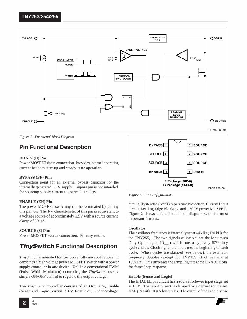
Figure 2. Functional Block Diagram.
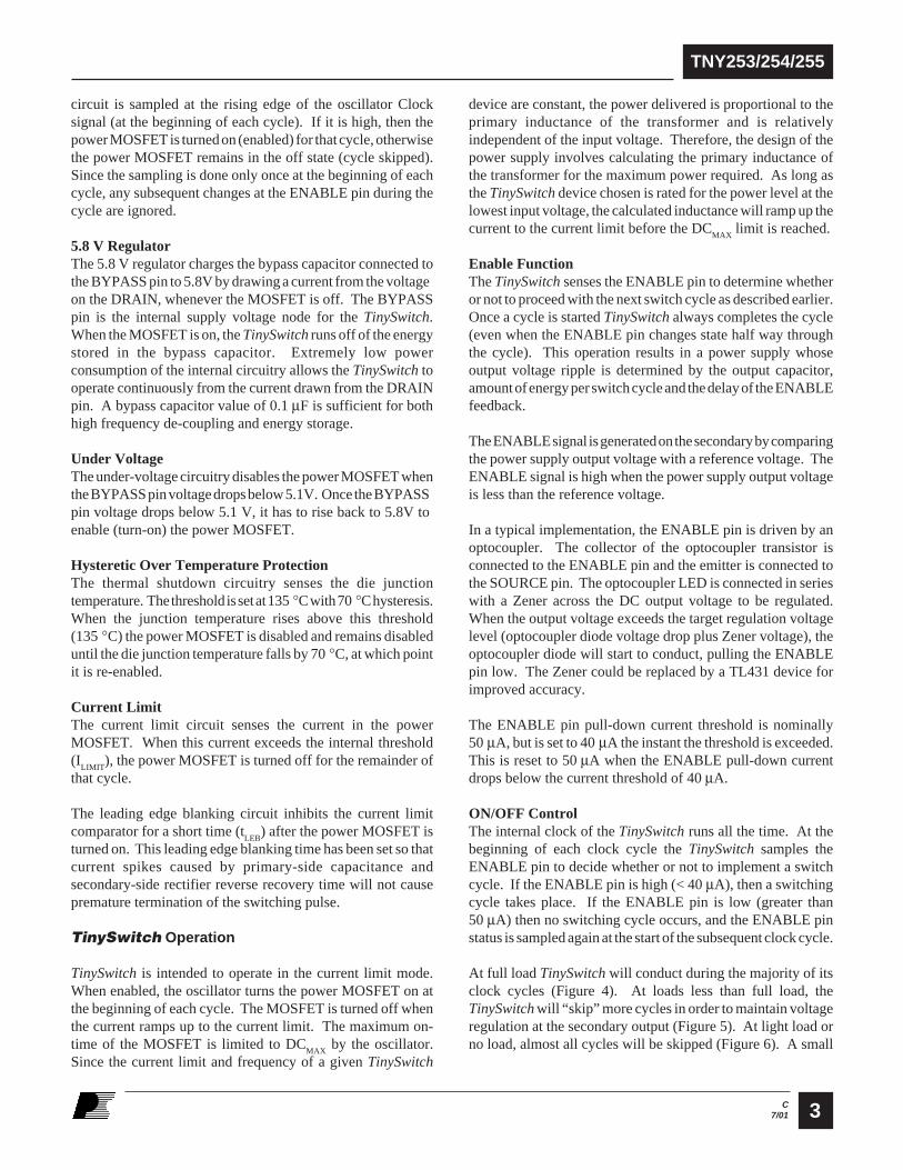
Figure 3. Pin Configuration.
Pin Functional Description
DRAIN (D) Pin:Power MOSFET drain connection. Provides internal operatingcurrent for both start-up and steady-state operation.
BYPASS (BP) Pin:Connection point for an external bypass capacitor for theinternally generated 5.8V supply. Bypass pin is not intendedfor sourcing supply current to external circuitry.
ENABLE (EN) Pin:The power MOSFET switching can be terminated by pullingthis pin low. The I-V characteristic of this pin is equivalent toa voltage source of approximately 1.5V with a source currentclamp of 50 µA.
SOURCE (S) Pin:Power MOSFET source connection. Primary return.
TinySwitch Functional Description
TinySwitch is intended for low power off-line applications. Itcombines a high voltage power MOSFET switch with a powersupply controller in one device. Unlike a conventional PWM(Pulse Width Modulator) controller, the TinySwitch uses asimple ON/OFF control to regulate the output voltage.
The TinySwitch controller consists of an Oscillator, Enable(Sense and Logic) circuit, 5.8V Regulator, Under-Voltage
circuit, Hysteretic Over Temperature Protection, Current Limitcircuit, Leading Edge Blanking, and a 700V power MOSFET.Figure 2 shows a functional block diagram with the mostimportant features.
OscillatorThe oscillator frequency is internally set at 44 kHz (130 kHz forthe TNY255). The two signals of interest are the MaximumDuty Cycle signal (DMAX) which runs at typically 67% dutycycle and the Clock signal that indicates the beginning of eachcycle. When cycles are skipped (see below), the oscillatorfrequency doubles (except for TNY255 which remains at130kHz). This increases the sampling rate at the ENABLE pinfor faster loop response.
Enable (Sense and Logic)The ENABLE pin circuit has a source follower input stage setat 1.5V. The input current is clamped by a current source setat 50 µA with 10 µA hysteresis. The output of the enable sense
PI-2197-061898
CLOCK
OSCILLATOR5.8 V5.1 V
SOURCE
S
R
Q
DCMAX
BYPASS
+
- VILIMIT
LEADINGEDGE
BLANKING
THERMALSHUTDOWN
+
-
DRAINREGULATOR5.8 V
UNDER-VOLTAGE
1.5 V + VTH
ENABLE
Q
50 µA
PI-2199-031501
ENABLE
8
5
7
6
DRAIN
SOURCE
SOURCE
SOURCE
1
4
2
3
SOURCE
SOURCEBYPASS
P Package (DIP-8) G Package (SMD-8)
C7/01
TNY253/254/255
3
circuit is sampled at the rising edge of the oscillator Clocksignal (at the beginning of each cycle). If it is high, then thepower MOSFET is turned on (enabled) for that cycle, otherwisethe power MOSFET remains in the off state (cycle skipped).Since the sampling is done only once at the beginning of eachcycle, any subsequent changes at the ENABLE pin during thecycle are ignored.
5.8 V RegulatorThe 5.8 V regulator charges the bypass capacitor connected tothe BYPASS pin to 5.8V by drawing a current from the voltageon the DRAIN, whenever the MOSFET is off. The BYPASSpin is the internal supply voltage node for the TinySwitch.When the MOSFET is on, the TinySwitch runs off of the energystored in the bypass capacitor. Extremely low powerconsumption of the internal circuitry allows the TinySwitch tooperate continuously from the current drawn from the DRAINpin. A bypass capacitor value of 0.1 µF is sufficient for bothhigh frequency de-coupling and energy storage.
Under VoltageThe under-voltage circuitry disables the power MOSFET whenthe BYPASS pin voltage drops below 5.1V. Once the BYPASSpin voltage drops below 5.1 V, it has to rise back to 5.8V toenable (turn-on) the power MOSFET.
Hysteretic Over Temperature ProtectionThe thermal shutdown circuitry senses the die junctiontemperature. The threshold is set at 135 °C with 70 °C hysteresis.When the junction temperature rises above this threshold(135 °C) the power MOSFET is disabled and remains disableduntil the die junction temperature falls by 70 °C, at which pointit is re-enabled.
Current LimitThe current limit circuit senses the current in the powerMOSFET. When this current exceeds the internal threshold(I
LIMIT), the power MOSFET is turned off for the remainder of
that cycle.
The leading edge blanking circuit inhibits the current limitcomparator for a short time (t
LEB) after the power MOSFET is
turned on. This leading edge blanking time has been set so thatcurrent spikes caused by primary-side capacitance andsecondary-side rectifier reverse recovery time will not causepremature termination of the switching pulse.
TinySwitch Operation
TinySwitch is intended to operate in the current limit mode.When enabled, the oscillator turns the power MOSFET on atthe beginning of each cycle. The MOSFET is turned off whenthe current ramps up to the current limit. The maximum on-time of the MOSFET is limited to DC
MAX by the oscillator.
Since the current limit and frequency of a given TinySwitch
device are constant, the power delivered is proportional to theprimary inductance of the transformer and is relativelyindependent of the input voltage. Therefore, the design of thepower supply involves calculating the primary inductance ofthe transformer for the maximum power required. As long asthe TinySwitch device chosen is rated for the power level at thelowest input voltage, the calculated inductance will ramp up thecurrent to the current limit before the DC
MAX limit is reached.
Enable FunctionThe TinySwitch senses the ENABLE pin to determine whetheror not to proceed with the next switch cycle as described earlier.Once a cycle is started TinySwitch always completes the cycle(even when the ENABLE pin changes state half way throughthe cycle). This operation results in a power supply whoseoutput voltage ripple is determined by the output capacitor,amount of energy per switch cycle and the delay of the ENABLEfeedback.
The ENABLE signal is generated on the secondary by comparingthe power supply output voltage with a reference voltage. TheENABLE signal is high when the power supply output voltageis less than the reference voltage.
In a typical implementation, the ENABLE pin is driven by anoptocoupler. The collector of the optocoupler transistor isconnected to the ENABLE pin and the emitter is connected tothe SOURCE pin. The optocoupler LED is connected in serieswith a Zener across the DC output voltage to be regulated.When the output voltage exceeds the target regulation voltagelevel (optocoupler diode voltage drop plus Zener voltage), theoptocoupler diode will start to conduct, pulling the ENABLEpin low. The Zener could be replaced by a TL431 device forimproved accuracy.
The ENABLE pin pull-down current threshold is nominally50 µA, but is set to 40 µA the instant the threshold is exceeded.This is reset to 50 µA when the ENABLE pull-down currentdrops below the current threshold of 40 µA.
ON/OFF ControlThe internal clock of the TinySwitch runs all the time. At thebeginning of each clock cycle the TinySwitch samples theENABLE pin to decide whether or not to implement a switchcycle. If the ENABLE pin is high (< 40 µA), then a switchingcycle takes place. If the ENABLE pin is low (greater than50 µA) then no switching cycle occurs, and the ENABLE pinstatus is sampled again at the start of the subsequent clock cycle.
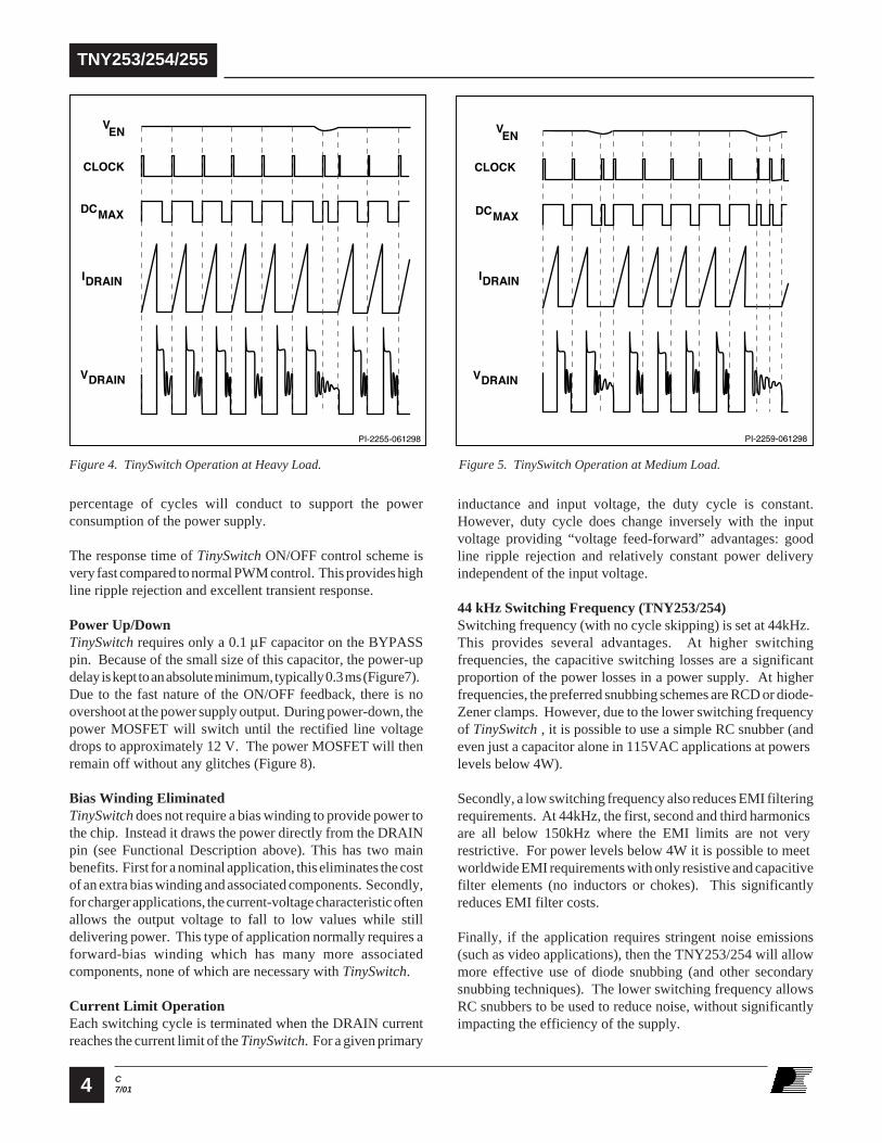
At full load TinySwitch will conduct during the majority of itsclock cycles (Figure 4). At loads less than full load, theTinySwitch will “skip” more cycles in order to maintain voltageregulation at the secondary output (Figure 5). At light load orno load, almost all cycles will be skipped (Figure 6). A small
C7/01
TNY253/254/255
4
Figure 4. TinySwitch Operation at Heavy Load. Figure 5. TinySwitch Operation at Medium Load.
V
DRAINV
EN
CLOCK
DC
DRAINI
MAX
PI-2255-061298
V
DRAINV
EN
CLOCK
DC
DRAINI
MAX
PI-2259-061298
percentage of cycles will conduct to support the powerconsumption of the power supply.
The response time of TinySwitch ON/OFF control scheme isvery fast compared to normal PWM control. This provides highline ripple rejection and excellent transient response.
Power Up/DownTinySwitch requires only a 0.1 µF capacitor on the BYPASSpin. Because of the small size of this capacitor, the power-updelay is kept to an absolute minimum, typically 0.3 ms (Figure7).Due to the fast nature of the ON/OFF feedback, there is noovershoot at the power supply output. During power-down, thepower MOSFET will switch until the rectified line voltagedrops to approximately 12 V. The power MOSFET will thenremain off without any glitches (Figure 8).
Bias Winding EliminatedTinySwitch does not require a bias winding to provide power tothe chip. Instead it draws the power directly from the DRAINpin (see Functional Description above). This has two mainbenefits. First for a nominal application, this eliminates the costof an extra bias winding and associated components. Secondly,for charger applications, the current-voltage characteristic oftenallows the output voltage to fall to low values while stilldelivering power. This type of application normally requires aforward-bias winding which has many more associatedcomponents, none of which are necessary with TinySwitch.
Current Limit OperationEach switching cycle is terminated when the DRAIN currentreaches the current limit of the TinySwitch. For a given primary
inductance and input voltage, the duty cycle is constant.However, duty cycle does change inversely with the inputvoltage providing “voltage feed-forward” advantages: goodline ripple rejection and relatively constant power deliveryindependent of the input voltage.
44 kHz Switching Frequency (TNY253/254)Switching frequency (with no cycle skipping) is set at 44kHz.This provides several advantages. At higher switchingfrequencies, the capacitive switching losses are a significantproportion of the power losses in a power supply. At higherfrequencies, the preferred snubbing schemes are RCD or diode-Zener clamps. However, due to the lower switching frequencyof TinySwitch , it is possible to use a simple RC snubber (andeven just a capacitor alone in 115VAC applications at powerslevels below 4W).
Secondly, a low switching frequency also reduces EMI filteringrequirements. At 44kHz, the first, second and third harmonicsare all below 150kHz where the EMI limits are not veryrestrictive. For power levels below 4W it is possible to meetworldwide EMI requirements with only resistive and capacitivefilter elements (no inductors or chokes). This significantlyreduces EMI filter costs.
Finally, if the application requires stringent noise emissions(such as video applications), then the TNY253/254 will allowmore effective use of diode snubbing (and other secondarysnubbing techniques). The lower switching frequency allowsRC snubbers to be used to reduce noise, without significantlyimpacting the efficiency of the supply.
C7/01
TNY253/254/255
5
Figure 6. TinySwitch Operation at Light Load.
Figure 7. TinySwitch Power-Up Timing Diagram.
Figure 8. TinySwitch Power Down Timing Diagram.
PI-2261-061198
V
DRAINV
EN
CLOCK
DC
DRAINI
MAX
130 kHz Switching Frequency (TNY255)The switching frequency (with no cycle skipping) is set at130kHz. This allows the TNY255 to deliver 10W while stillusing the same size, low cost transformer (EE16) as used by theTNY253/254 for lower power applications.
BYPASS Pin CapacitorThe BYPASS pin uses a small 0.1 µF ceramic capacitor fordecoupling the internal power supply of the TinySwitch.
Application Examples
Television Standby
TinySwitch is an ideal solution for low cost, high efficiencystandby power supplies used in consumer electronic productssuch as TVs. Figure9 shows a 7.5 V, 1.3 W flyback circuit thatuses TNY253 for implementing a TV standby supply. Thecircuit operates from the DC high voltage already availablefrom the main power supply. This input voltage can range from120 to 375VDC depending on the input AC voltage range thatthe TV is rated for. Capacitor C1 filters the high voltage DCsupply, and is necessary only if there is a long trace length fromthe source of the DC supply to the inputs of the TV standbycircuit. The high voltage DC bus is applied to the seriescombination of the primary winding of T1 and the integratedhigh voltage MOSFET inside the TNY253. The low operatingfrequency of the TNY253 (44kHz), allows a low cost snubbercircuit C2 and R1 to be used in place of a primary clamp circuit.In addition to limiting the DRAIN turn off voltage spike to asafe value, the RC snubber also reduces radiated video noise by
lowering the dv/dt of the DRAIN waveform, which is critical forvideo applications such as TV and VCR. On fixed frequencyPWM and RCC circuits, use of a snubber will result in anundesirable fixed AC switching loss that is independent of load.The ON/OFF control on the TinySwitch eliminates this problemby scaling the effective switching frequency and therefore,switching loss linearly with load. Thus the efficiency of thesupply stays relatively constant down to a fraction of a watt ofoutput loading.
The secondary winding is rectified and filtered by D1 and C4 tocreate the 7.5V output. L1 and C5 provide additional filtering.The output voltage is determined by the sum of the optocouplerU2 LED forward drop (~ 1 V) and Zener diode VR1 voltage.The resistor R2, maintains a bias current through the Zener toimprove its voltage tolerance.
V
DRAINV
IN
PI—
2253
-062
398
0 .2
Time (ms).4 .6 .8 1
0 V
0 V
V
DRAINV
IN
12 V
PI—
2251
-062
398
12 V
0 100
Time (ms)200 300 400 500
0 V
0 V
C7/01
TNY253/254/255
6
Figure 9. 1.3 W TV Stand-by Circuit using TNY253.
Figure 10. 10 W PC Stand-by Supply Circuit.
PC Standby
The TNY255 was designed specifically for applications such asPC standby, which require up to 10W of power from 230VACor 100/115VAC with doubler circuit. The TNY255 operates at130kHz as opposed to 44kHz for TNY253/254. The higherfrequency operation allows the use of a low cost EE16 coretransformer up to the 10W level. Figure10 shows a 5V, 10Wcircuit for such an application. The circuit operates from thehigh voltage DC supply already available from the main powersupply. Capacitor C1 filters the high voltage DC supply, and isnecessary only if there is a long trace length from the source ofthe DC supply to the inputs of the PC standby circuit. The highvoltage DC bus is applied to the primary winding of T1 in series
with the integrated high voltage MOSFET inside the TNY255.The diode D1, capacitor C2 and resistor R1 comprise the clampcircuit that limits the turn-off voltage spike on the TinySwitchDRAIN pin to a safe value. The secondary winding is rectifiedand filtered by D2 and C4 to provide the 5V ouput. Additionalfiltering is provided by L1 and C5. The output voltage isdetermined by the sum of the optocoupler U2 LED forwarddrop (~ 1V) and Zener diode VR1 voltage. The resistor R2,maintains a bias current through the Zener to improve itsvoltage tolerance.
Cellular Phone Charger
The TinySwitch is well suited for applications that require a
PI-2242-082898
TinySwitchD
S
EN
BP
+ 5 V
RTN
C10.01 µF
1 kV
C30.1 µF
240-375 VDC
R1150 kΩ
1 W
U2LTV817
D2SB540
L110 µH
C42700 µF
6.3 V
C5220 µF10 V
VR11N5229B
U1TNY255P
C24700 pF
1 kV
T11
4 8
10
R268 Ω
D11N4937
Optional
PI-2246-082898
DC IN120-375 VDC
TinySwitchD
S
EN
BP
+
–
+ 7.5 V
RTN
C30.1 µF
R21 kΩ
VR11N5235B
C10.01 µF
1 kV
R1100 Ω 1/2 W
C256 pF1 kV
D11N4934
L115 µH
C547 µF10 V
C4330 µF10 V
U1TNY253P
T1
U2SFH615-2
C6680 pF
Y1 Safety
1
4 8
10
Optional
C7/01
TNY253/254/255
7
Figure 11. 3.6 W Constant Voltage-Constant Current Cellular Phone Charger Circuit.
constant voltage and constant current output. TinySwitch isalways powered from the input high voltage, therefore it doesnot require bias winding for power. Consequently, its operationis not dependent on the level of the output voltage. This allowsfor constant current charger designs that work down to zerovolts on the output.
Figure11 shows a 5.2V, 3.6W cellular phone charger circuitthat uses the TNY254 and provides constant voltage and constantcurrent output over an universal input (85 to 265VAC) range.The AC input is rectified and filtered by D1 - D4, C1 and C2 to
create a high voltage DC bus connected to T1 in series with thehigh voltage MOSFET inside the TNY254. The inductor L1forms a π-filter in conjunction with C1 and C2. The resistor R1damps resonances in the inductor L1. The low frequency ofoperation of TNY254 (44kHz) allows use of the simple π-filterdescribed above in combination with a single Y1-capacitor C8to meet worldwide conducted EMI standards. The diode D6,capacitor C4 and resistor R2 comprise the clamp circuit thatlimits the turn-off voltage spike on the TinySwitch DRAIN pinto a safe value. The secondary winding is rectified and filteredby D5 and C5 to provide the 5.2V output. Additional filtering
Figure 12. 0.5 W Open Loop AC Adapter Circuit.
PI-2244-082898
TinySwitchD
S
EN
BP
+ 5.2 V
RTND11N4005
C16.8 µF400 V
Fusible
RF110 Ω
C30.1 µF
85-265 VAC
L1560 µH
D21N4005
D31N4005
D41N4005
R2100 kΩ
1 W
U2LTV817
D5FR201
L23.3 µH
C5220 µF25 V
C24.7 µF400 V
C6220 µF16 V
R7100 Ω
R322 Ω
R41 Ω1 W
R947 Ω
Q12N3904
R8820 Ω
VR11N5230B
4.7 V
C82.2 nF
Y1 Safety
U1TNY254P
C42200 pF
D61N4937
R60.82 Ω1/2 W
T1
R11.2 kΩ
1
2 5
10
R518 Ω1/8 W
PI-2190-031501
TinySwitchD
S
EN
BP
+ 9 V
RTN
D11N4004
C12.2 µF200 V
Fusible
RF11.8 Ω
C468 pF1 KV
115 VAC± 15%
R2100 Ω
D21N4004
C30.1 µF
D31N3934
C6100 µF
16V
C22.2 µF200 V
VR11N5239B
C52.2 nF
Y1 Safety
U1TNY253P
T11
5 6
10
C7/01
TNY253/254/255
8
is provided by L2 and C6. The output voltage is determined bythe sum of the optocoupler U2 LED forward drop (~ 1V) andZener diode VR1 voltage. The resistor R8, maintains a biascurrent through the Zener to improve its voltage tolerance.
A simple constant current circuit is implemented using the VBE
of transistor Q1 to sense the voltage across the current senseresistor R4, which can be made up of one or more resistors toachieve the appropriate value. R3 is a base current limitingresistor. When the drop across R4 exceeds the V
BE of transistor
Q1, it turns on and takes over the control of the loop by drivingthe optocoupler LED. R6 drops an additional voltage to keep thecontrol loop in operation down to zero volts on the output. Withthe output shorted, the drop across R4 and R6 (~ 1.5V) issufficient to keep the Q1 and LED circuit active. Resistors R7and R9 limit the forward current that could be drawn throughVR1 by Q1 under output short circuit conditions, due to thevoltage drop across R6 and R4.
AC Adapter
Many consumer electronic products utilize low power 50/60Hztransformer based AC adapters. The TinySwitch can costeffectively replace these linear adapters with a solution that islighter, smaller and more energy efficient . Figure12 shows a9V, 0.5W AC adapter circuit using the TNY253. This circuitoperates from a 115VAC input. To save cost, this circuit runswithout any feedback, in discontinuous conduction mode todeliver constant power output relatively independent of inputvoltage. The output voltage is determined by the voltage dropacross Zener diode VR1. The primary inductance of thetransformer is chosen to deliver a power that is in excess of therequired output power by at least 50% to allow for componenttolerances and to maintain some current through the Zener VR1at full load. At no load, all of the power is delivered to the Zenerwhich should be rated and heat sinked accordingly. In spite ofa constant power consumption from the mains input, this solutionis still significantly more efficient than linear adapters up tooutput power levels of approximately 1W.
The AC input is rectified by diodes D1 and D2. D2 is used toreduce conducted EMI by only allowing noise onto the neutralline during diode conduction. The rectified AC is then filteredby capacitors C1 and C2 to generate a high voltage DC bus,which is applied to the series combination of the primarywinding of T1 and the high voltage MOSFET inside the TNY253.The resistor R2 along with capacitors C1 and C2 form a π-filterwhich is sufficient for meeting EMI conducted emissions atthese power levels. C5 is a Y-capacitor which is used to reducecommon mode EMI. Due to the 700V rating of the TinySwitchMOSFET, a simple capacitive snubber (C4) is adequate to limitthe leakage inductance spike in 115VAC applications, at lowpower levels. The secondary winding is rectified and filtered byD3 and C6.
Key Application Considerations
For the most up to date information visit our Web siteat: www.powerint.com
Design
Output Power RangeThe power levels shown in the TinySwitch Selection Guide(Table 1) are approximate, recommended output power rangesthat will provide a cost optimum design and are based onfollowing assumptions:
1. The minimum DC input voltage is 90 V or higher for85VAC input or 240V or higher for 230 VAC input or115VAC input with a voltage doubler.
2. The TinySwitch is not thermally limited-the source pins aresoldered to sufficient copper area to keep the die temperatureat or below 100 °C. This limitation does not usually applyto TNY253 and TNY254.
The maximum power capability of a TinySwitch depends on thethermal environment, transformer core size and design(continuous or discontinuous), efficiency required, minimumspecified input voltage, input storage capacitance, outputvoltage, output diode forward drop, etc., and can be differentfrom the values shown in the selection guide.
Audible NoiseAt loads other than maximum load, the cycle skipping modeoperation used in TinySwitch can generate audio frequencycomponents in the transformer. This can cause the transformerto produce audio noise. Transformer audible noise can bereduced by utilizing appropriate transformer constructiontechniques and decreasing the peak flux density. For moreinformation on audio suppression techniques, please checkthe Application Notes section on our Web site atwww.powerint.com.
Ceramic capacitors that use dielectrics such as Z5U, when usedin clamp and snubber circuits, can also generate audio noise dueto electrostriction and piezo-electric effects. If this is the case,replacing them with a capacitor having a different type ofdielectric is the simplest solution. Polyester film capacitor is agood alternative.
Short Circuit CurrentThe TinySwitch does not have an auto-restart feature. As aresult, TinySwitch will continue to deliver power to the loadduring output short circuit conditions. In the worst case, peakshort circuit current is equal to the primary current limit (I
LIMIT)
multiplied by the turns ratio of the transformer (Np/N
s). In a
typical design the average current is 25 to 50% lower than thispeak value. At the power levels of TinySwitch this is easily
C7/01
TNY253/254/255
9
Figure 13. Recommended PC Layout for the TinySwitch.
accommodated by rating the output diode to handle the shortcircuit current. The short circuit current can be minimized bychoosing the smallest (lowest current limit) TinySwitch for therequired power.
Layout
Single Point GroundingUse a single point ground connection at the SOURCE pin for theBYPASS pin capacitor and the Input Filter Capacitor (seeFigure 13).
Primary Loop AreaThe area of the primary loop that connects the input filtercapacitor, transformer primary and TinySwitch together, shouldbe kept as small as possible.
Primary Clamp CircuitA clamp or snubber circuit is used to minimize peak voltage andringing on the DRAIN pin at turn-off. This can be achieved byusing an RC snubber for less than 3 W or an RCD clamp asshown in Figure 13 for higher power. A Zener and diode clampacross the primary or a single 550V Zener clamp from DRAINto SOURCE can also be used. In all cases care should be takento minimize the circuit path from the snubber/clamp componentsto the transformer and TinySwitch.
Thermal ConsiderationsCopper underneath the TinySwitch acts not only as a single pointground, but also as a heatsink. The hatched area shown inFigure13 should be maximized for good heat-sinking ofTinySwitch and output diode.
Y-CapacitorThe placement of the Y-capacitor should be directly from theprimary single point ground to the common/return terminal onthe secondary side. Such placement will maximize the EMIbenefit of the Y-capacitor.
OptocouplerIt is important to maintain the minimum circuit path from theoptocoupler transistor to the TinySwitch ENABLE and SOURCEpins to minimize noise coupling.
Output DiodeFor best performance, the area of the loop connecting thesecondary winding, the Output Diode and the Output FilterCapacitor, should be minimized. See Figure13 for optimizedlayout. In addition, sufficient copper area should be providedat the anode and cathode terminals of the diode to adequatelyheatsink the diode under output short circuit conditions.
Input and Output Filter CapacitorsThere are constrictions in the traces connected to the input andoutput filter capacitors. These constrictions are present for tworeasons. The first is to force all the high frequency currents toflow through the capacitor (if the trace were wide then it couldflow around the capacitor). Secondly, the constrictions minimizethe heat transferred from the TinySwitch to the input filtercapacitor and from the secondary diode to the output filtercapacitor. The common/return (the negative output terminal inFigure13) terminal of the output filter capacitor should beconnected with a short, low resistance path to the secondarywinding. In addition, the common/return output connectionshould be taken directly from the secondary winding pin andnot from the Y-capacitor connection point.
TOP VIEW
PI-2176-071398
Y1-Capacitor
Opto-coupler
CBP
D
ENBP
TinySwitch
+
–
HV
+– DCOut
Input Filter Capacitor Output Filter Capacitor
Safety Spacing
Transformer
Maximize hatched copper areas ( ) for optimum heat sinking
S
S
PRI SEC
C7/01
TNY253/254/255
10
Storage Temperature ..................................... -65 to 150 °COperating Junction Temperature(2) ................ -40 to 150 °CLead Temperature(3) ................................................ 260 °CThermal Impedance (θ
JA) ................ 45 °C/W(4), 35 °C/W(5)
Thermal Impedance (θJC
) ..................................... 11 °C/W
4. Soldered to 0.36 sq. inch (232 mm2), 2 oz. (610 gm/m2) copper clad.5. Soldered to 1 sq. inch (645 mm2), 2 oz. (610 gm/m2) copper clad.
ABSOLUTE MAXIMUM RATINGS(1)
DRAIN Voltage ....................................... - 0.3 V to 700 VPeak DRAIN Current (TNY253/4) ........................400 mAPeak DRAIN Current (TNY255) ........................... 530 mAENABLE Voltage ........................................ - 0.3 V to 9 VENABLE Current ................................................... 100 mABYPASS Voltage .......................................... -0.3 V to 9 V
1. All voltages referenced to SOURCE, TA = 25 °C.
2. Normally limited by internal circuitry.3. 1/16" from case for 5 seconds.
NOTES:A. For a threshold with a negative value, negative hysteresis is a decrease in magnitude of the corresponding threshold.
B. Total current consumption is the sum of IS1
and IDSS
when ENABLE pin is shorted to ground (MOSFET not switching) and the sum of I
S2 and I
DSS when ENABLE pin is open (MOSFET switching).
C. Since the output MOSFET is switching, it is difficult to isolate the switching current from the supply current at the DRAIN. An alternative is to measure the BYPASS pin current at 6.2 V.
D. Bypass pin is not intended for sourcing supply current to external circuitry.
E. See typical performance characteristics section for BYPASS pin start-up charging waveform.
F. For current limit at other di/dt values, refer to current limit vs. di/dt curve under typical performance characteristics.
G. This parameter is derived from the change in current limit measured at 5X and 10X of the di/dt shown in the ILIMIT
specification.
Figure 14. TinySwitch General Test Circuit.
PI-2211-061898
0.1 µF
10 V50 V
470 Ω5 W S2
S1
470 Ω
NOTE: This test circuit is not applicable for current limit or output characteristic measurements.
D EN
BPS
S
S
S
S
ConditionsParameter Symbol SOURCE = 0 V; T
J = -40 to 125 °C
See Figure 14(Unless Otherwise Specified)
50
0.5
tEN
tDST
V
µs
µs
DRAIN SupplyVoltage
Output EnableDelay
Output DisableSetup Time
Min Typ Max Units
OUTPUT (cont.)
See Figure 16TNY253TNY254TNY255 10
14
C7/01
TNY253/254/255
13
1.1
1.0
0.9-50 -25 0 25 50 75 100 125 150
Junction Temperature (°C)
Bre
akd
ow
n V
olt
age
(V)
(No
rmal
ized
to
25
°C)
BREAKDOWN vs. TEMPERATURE
PI-
2213
-040
901
Typical Performance Characteristics
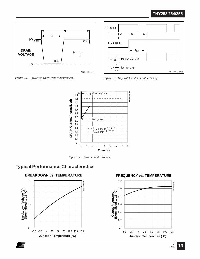
Figure 17. Current Limit Envelope.
Figure 15. TinySwitch Duty Cycle Measurement.
PI-2194-062398
ENABLE
tP
tEN
tP =
1
2fOSCfor TNY253/254
DCMAX
tP =
1
fOSCfor TNY255
Figure 16. TinySwitch Output Enable Timing.
1.2
1.0
0.8
0.6
0.4
0.2
0-50 -25 0 25 50 75 100 125
Junction Temperature (°C)
FREQUENCY vs. TEMPERATUREP
I-22
38-0
3300
1
Ou
tpu
t F
req
uen
cy(N
orm
aliz
ed t
o 2
5 °C
)0.8
1.31.21.1
0.90.8
1.0
00 1 2 6 83
Time ( s)
DR
AIN
Cu
rren
t (n
orm
aliz
ed)
PI-
2248
-090
198
4 5 7
0.70.60.50.40.30.20.1
ILIMIT(MAX) @ 25 °CILIMIT(MIN) @ 25 °C
IINIT(MIN)
tLEB (Blanking Time)
PI-2048-033001
DRAINVOLTAGE
HV
0 V
90%
10%
90%
t2
t1
D = t1t2
C7/01
TNY253/254/255
14
Typical Performance Characteristics (Continued)
1.2
1.0
0.8
0.6
0.4
0.2
0.00 12.5 25 37.5 50 62.5 75 87.5 100
di/dt in mA/µs
TNY253 CURRENT LIMIT vs. di/dt
PI-
2230
-082
798
Cu
rren
t L
imit
(No
rmal
ized
to
12.
5 m
A/µ
s)
1.4
1.2
1.0
0.8
0.6
0.4
0.2
0.00 50 100 150 200 250
di/dt in mA/µs
TNY254 CURRENT LIMIT vs. di/dt
PI-
2232
-082
798
Cu
rren
t L
imit
(No
rmal
ized
to
25
mA
/ µs)
1.4
1.2
1.0
0.8
0.6
0.4
0.2
0.00 160 320 480 640 800
di/dt in mA/µs
TNY255 CURRENT LIMIT vs. di/dt
PI-
2234
-082
798
Cu
rren
t L
imit
(No
rmal
ized
to
80
mA
/µs)
1.4
1.2
1.0
0.8
0.6
0.4
0.2
0.0-50 -25 0 25 50 75 100 125
Junction Temperature (°C)
CURRENT LIMIT vs. TEMPERATURE
PI-
2236
-033
001
Cu
rren
t L
imit
(No
rmal
ized
to
25
°C)
1.4
6
5
4
3
2
1
0
0 0.2 0.4 0.6 0.8 1.0
Time (ms)
BYPASS PIN START-UP WAVEFORM
PI-
2240
-082
898
BY
PA
SS
Pin
Vo
ltag
e (V
)
7
DRAIN Voltage (V)
Dra
in C
urr
ent
(mA
)
OUTPUT CHARACTERISTIC300
250
200
100
50
150
00 2 4 6 8 10
TCASE=25 °CTCASE=100 °C P
I-22
21-0
3300
1
TNY253 1.00TNY254 1.00TNY255 1.33
Scaling Factors:
C7/01
TNY253/254/255
15
PI-2076-040501
1
A
K
J1
4
L
G
8 5
C
N
DIP-8
D S .004 (.10)
J2
-E-
-D-
B
-F-
DIM
A
B
C
G
H
J1
J2
K
L
M
N
P
Q
inches
0.370-0.385
0.245-0.255
0.125-0.135
0.015-0.040
0.120-0.135
0.060 (NOM)
0.014-0.022
0.010-0.012
0.090-0.110
0.030 (MIN)
0.300-0.320
0.300-0.390
0.300 BSC
mm
9.40-9.78
6.22-6.48
3.18-3.43
0.38-1.02
3.05-3.43
1.52 (NOM)
0.36-0.56
0.25-0.30
2.29-2.79
0.76 (MIN)
7.62-8.13
7.62-9.91
7.62 BSC
Notes:1. Package dimensions conform to JEDEC specification MS-001-AB for standard dual in-line (DIP) package .300 inch row spacing (PLASTIC) 8 leads (issue B, 7/85).2. Controlling dimensions are inches.3. Dimensions shown do not include mold flash or other protrusions. Mold flash or protrusions shall not exceed .006 (.15) on any side.4. D, E and F are reference datums on the molded body.
Notes:1. Package dimensions conform to JEDEC specification MS-001-AB (issue B, 7/85) except for lead shape and size.2. Controlling dimensions are inches. 3. Dimensions shown do not include mold flash or other protrusions. Mold flash or protrusions shall not exceed .006 (.15) on any side.4. D, E and F are reference datums on the molded body.
K
Gα
H
.004 (.10)
J4
P
.010 (.25) M A S
Heat Sink is 2 oz. Copper As Big As Possible
.420
.046 .060 .060 .046
.080Pin 1
.086.186
.286
Solder Pad Dimensions
C7/01
TNY253/254/255
17
Notes
C7/01
TNY253/254/255
18
Notes
C7/01
TNY253/254/255
19
Notes
C7/01
TNY253/254/255
20
Notes-
1) Leading edge blanking time (tLEB
) typical and minimum values increased to improve design flexibility.
WORLD HEADQUARTERSAMERICASPower Integrations, Inc.5245 Hellyer AvenueSan Jose, CA 95138 USAMain: +1 408-414-9200Customer Service:Phone: +1 408-414-9665Fax: +1 408-414-9765e-mail: [email protected]
For the latest updates, visit our Web site: www.powerint.comPower Integrations reserves the right to make changes to its products at any time to improve reliability or manufacturability.Power Integrations does not assume any liability arising from the use of any device or circuit described herein, nor does itconvey any license under its patent rights or the rights of others.
CHINAPower IntegrationsInternational Holdings, Inc.Rm# 1705, Bao Hua Bldg.1016 Hua Qiang Bei LuShenzhen, Guangdong 518031ChinaPhone: +86-755-367-5143Fax: +86-755-377-9610e-mail: [email protected]
INDIA (Technical Support)Innovatech#1, 8th Main RoadVasanthnagarBangalore, India 560052Phone: +91-80-226-6023Fax: +91-80-228-9727e-mail: [email protected]