34
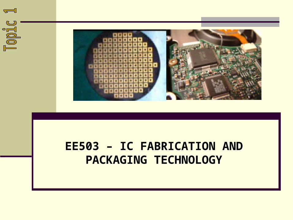
EE503 – IC FABRICATION AND PACKAGING TECHNOLOGY
| Date post: | 07-Dec-2015 |
| Category: |
Documents |
| Upload: | prevenamaniam |
| View: | 33 times |
| Download: | 2 times |
EE503 – IC FABRICATION AND PACKAGING TECHNOLOGY
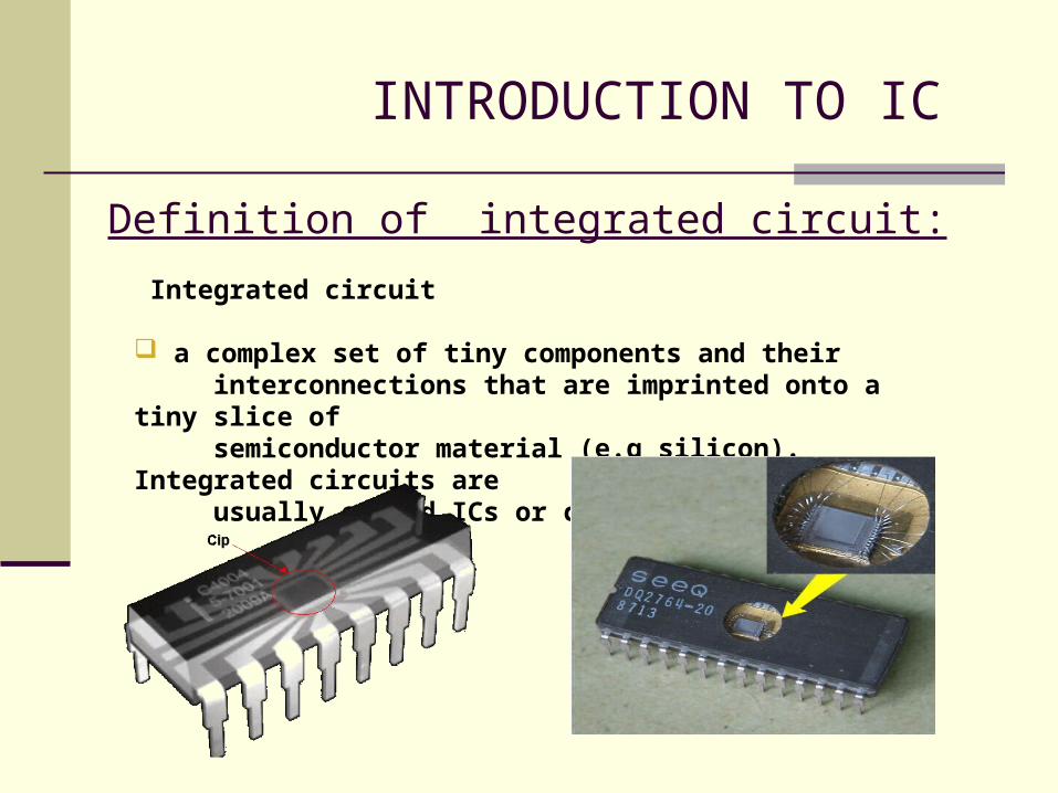
INTRODUCTION TO IC
Integrated circuit
a complex set of tiny components and their interconnections that are imprinted onto a tiny slice of semiconductor material (e.g silicon). Integrated circuits are usually called ICs or chips.
Definition of integrated circuit:

History of Semiconductor IndustryHistory of Semiconductor Industry
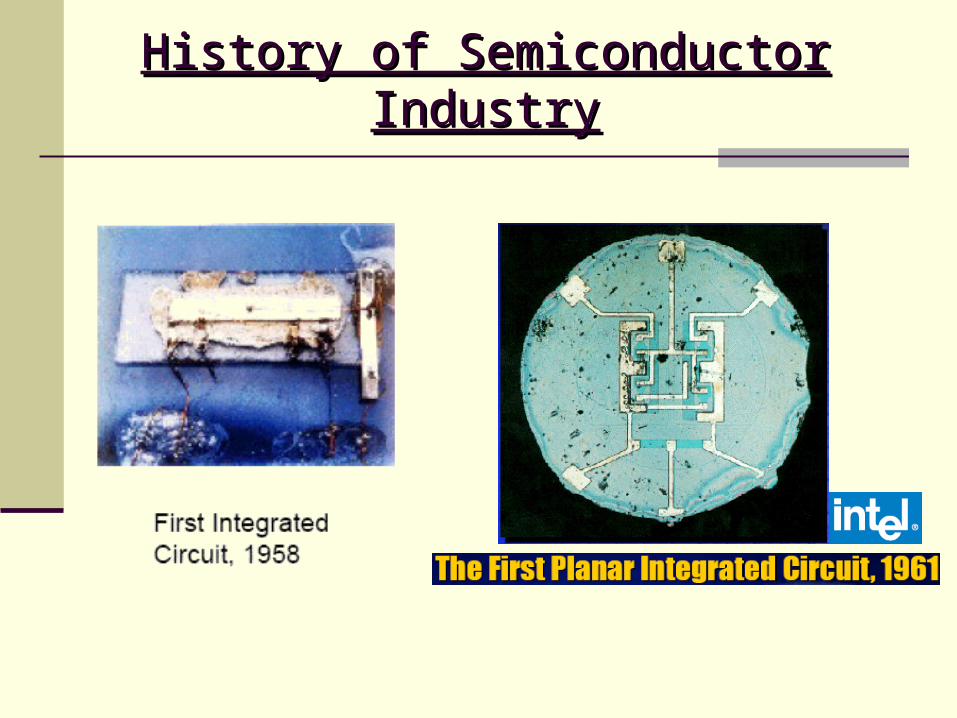
History of Semiconductor IndustryHistory of Semiconductor Industry
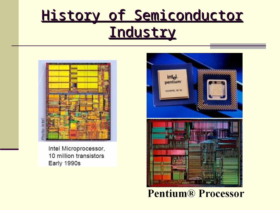
History of Semiconductor IndustryHistory of Semiconductor Industry
Functions of IC
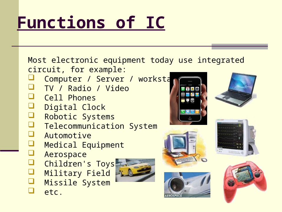
Most electronic equipment today use integrated circuit, for example: Computer / Server / workstation TV / Radio / Video Cell Phones Digital Clock Robotic Systems Telecommunication System Automotive Medical Equipment Aerospace Children's Toys Military Field Missile System etc.

Advantages of IC
i. Small ii. Low Cost
iii. Very Low Weight
iv. Low power consumption v. High reliability
vi. Easy replacement
Microelectronics EvolutionMicroelectronics Evolution
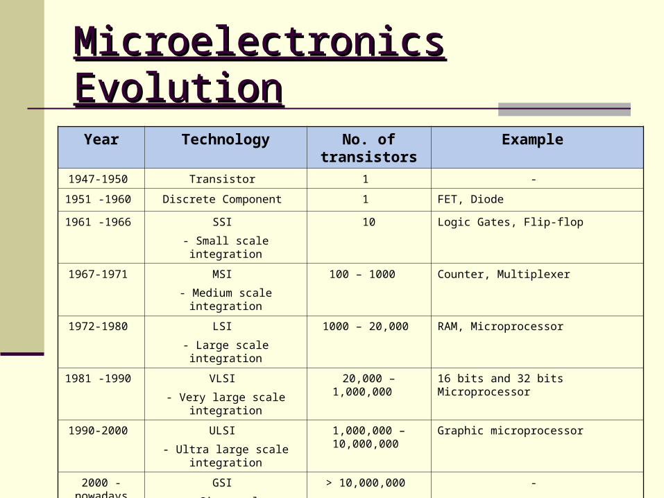
Year Technology No. of transistors
Example
1947-1950 Transistor 1 -
1951 -1960 Discrete Component 1 FET, Diode
1961 -1966 SSI
- Small scale integration
10 Logic Gates, Flip-flop
1967-1971 MSI
- Medium scale integration
100 – 1000 Counter, Multiplexer
1972-1980 LSI
- Large scale integration
1000 – 20,000 RAM, Microprocessor
1981 -1990 VLSI
- Very large scale integration
20,000 – 1,000,000 16 bits and 32 bits Microprocessor
1990-2000 ULSI
- Ultra large scale integration
1,000,000 – 10,000,000
Graphic microprocessor
2000 - nowadays
GSI
- Giga scale integration
> 10,000,000 -
IC Integration ScalesIC Integration Scales
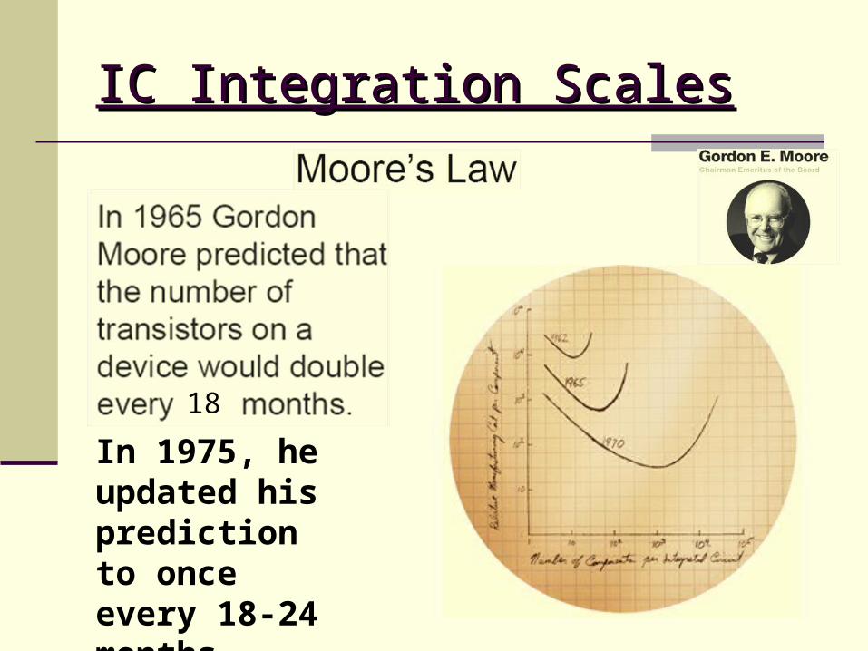
In 1975, he updated his prediction to once every 18-24 months.
18
IC Integration ScalesIC Integration Scales
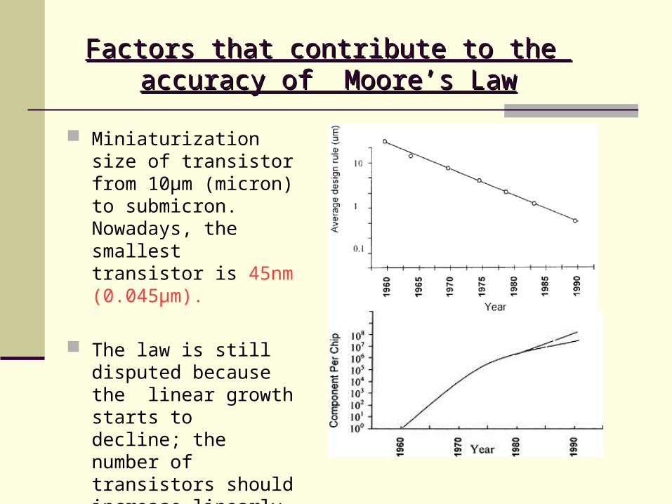
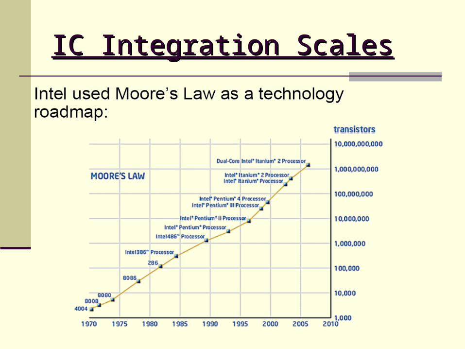
Miniaturization size of transistor from 10µm (micron) to submicron. Nowadays, the smallest transistor is 45nm (0.045µm).
The law is still disputed because the linear growth starts to decline; the number of transistors should increase linearly, but it starts to decrease after 1970.
Factors that contribute to the Factors that contribute to the accuracy of Moore’s Lawaccuracy of Moore’s Law

Classification of Integrated CircuitClassification of Integrated Circuit
In general, IC can be classified into FOUR (4) categories :
Classification based on the fabrication method
Classification based on transistor type
Classification based on circuits function
Classification based on design methodology
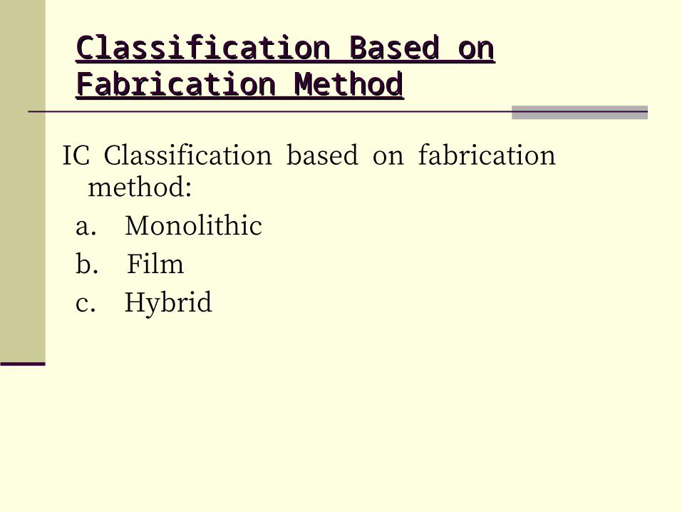
IC Classification based on fabrication method:
a. Monolithic
b. Film
c. Hybrid
Classification Based on Fabrication MethodClassification Based on Fabrication Method
Classification Based on Fabrication MethodClassification Based on Fabrication Method
a. Monolithica. Monolithic
The word ‘monolithic’ is derived from the Greek word monos, meaning ’single’ and lithos, meaning ‘stone’.
A monolithic IC is a miniaturized electronic circuit including both active and passive components and their interconnections are being manufactured in the surface of a thin substrate of semiconductor material.
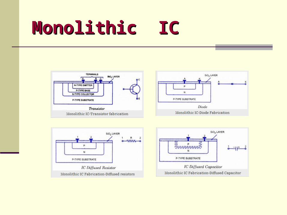
Monolithic ICMonolithic IC
Monolithic ICMonolithic IC
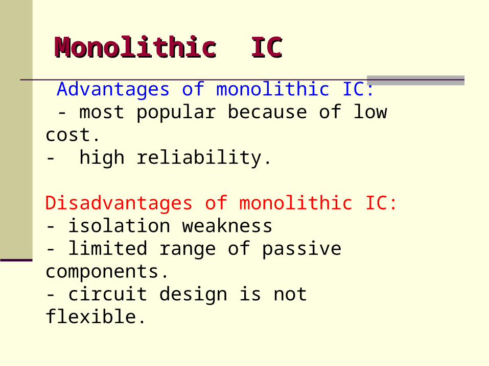
-Advantages of monolithic IC:-- most popular because of low cost.- high reliability.
Disadvantages of monolithic IC:- isolation weakness - limited range of passive components.- circuit design is not flexible.
Classification Based on Fabrication MethodClassification Based on Fabrication Method
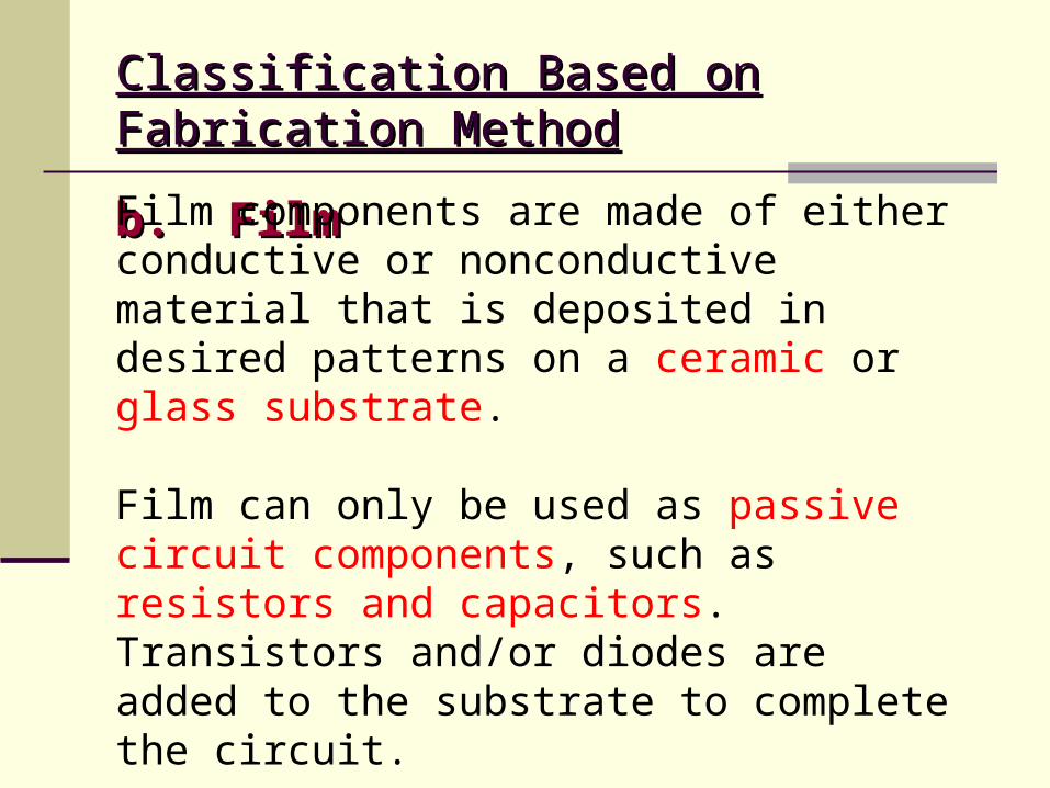
b. Filmb. FilmFilm components are made of either conductive or nonconductive material that is deposited in desired patterns on a ceramic or glass substrate.
Film can only be used as passive circuit components, such as resistors and capacitors. Transistors and/or diodes are added to the substrate to complete the circuit.
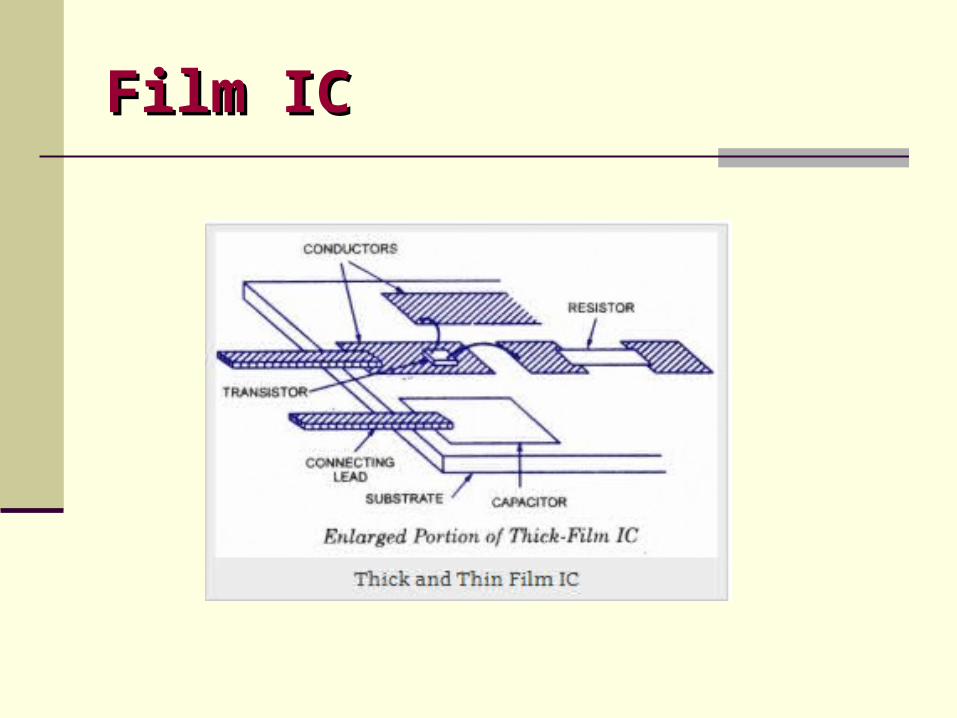
Film ICFilm IC
Classification Based on Fabrication MethodClassification Based on Fabrication Method
c. Hybrid ICc. Hybrid IC
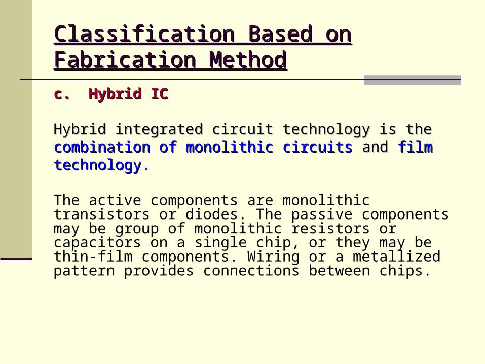
Hybrid integrated circuit technology is the Hybrid integrated circuit technology is the combination of monolithic circuits combination of monolithic circuits and and film film technology.technology.
The active components are monolithic transistors or diodes. The passive components may be group of monolithic resistors or capacitors on a single chip, or they may be thin-film components. Wiring or a metallized pattern provides connections between chips.
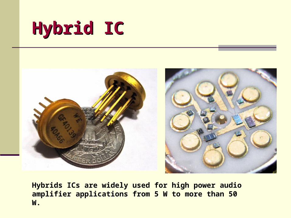
Hybrid ICHybrid IC
Hybrids ICs are widely used for high power audio amplifier applications from 5 W to more than 50 W.
Hybrid ICHybrid IC
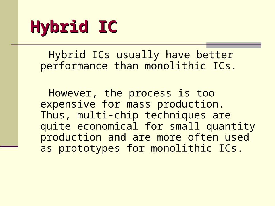
Hybrid ICs usually have better performance than monolithic ICs.
However, the process is too expensive for mass production. Thus, multi-chip techniques are quite economical for small quantity production and are more often used as prototypes for monolithic ICs.
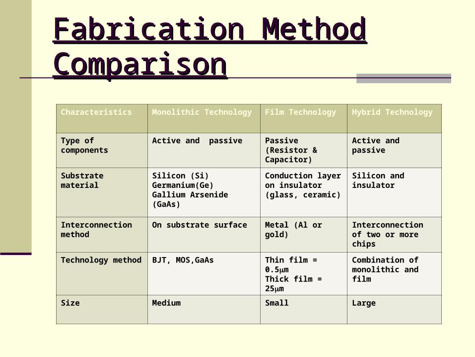
Fabrication Method ComparisonFabrication Method Comparison
Characteristics Monolithic Technology Film Technology Hybrid Technology
Type of components Active and passive Passive (Resistor & Capacitor)
Active and passive
Substrate material Silicon (Si)Germanium(Ge)Gallium Arsenide (GaAs)
Conduction layer on insulator (glass, ceramic)
Silicon and insulator
Interconnection method
On substrate surface Metal (Al or gold) Interconnection of two or more chips
Technology method BJT, MOS,GaAs Thin film = 0.5mThick film = 25m
Combination of monolithic and film
Size Medium Small Large
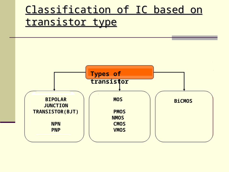
Classification of IC based on transistor typeClassification of IC based on transistor type
Types of transistor
MOS
PMOSNMOS CMOSVMOS
BiCMOS BIPOLAR JUNCTION
TRANSISTOR(BJT)
NPNPNP
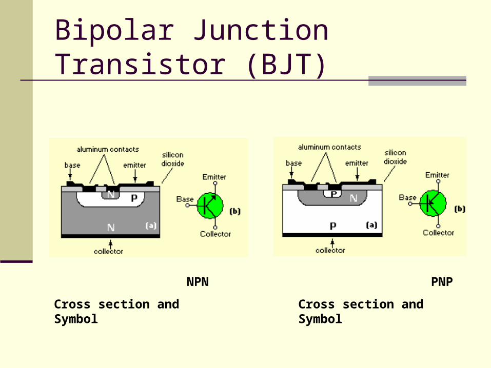
Bipolar Junction Transistor (BJT)
NPN
Cross section and Symbol
PNP
Cross section and Symbol
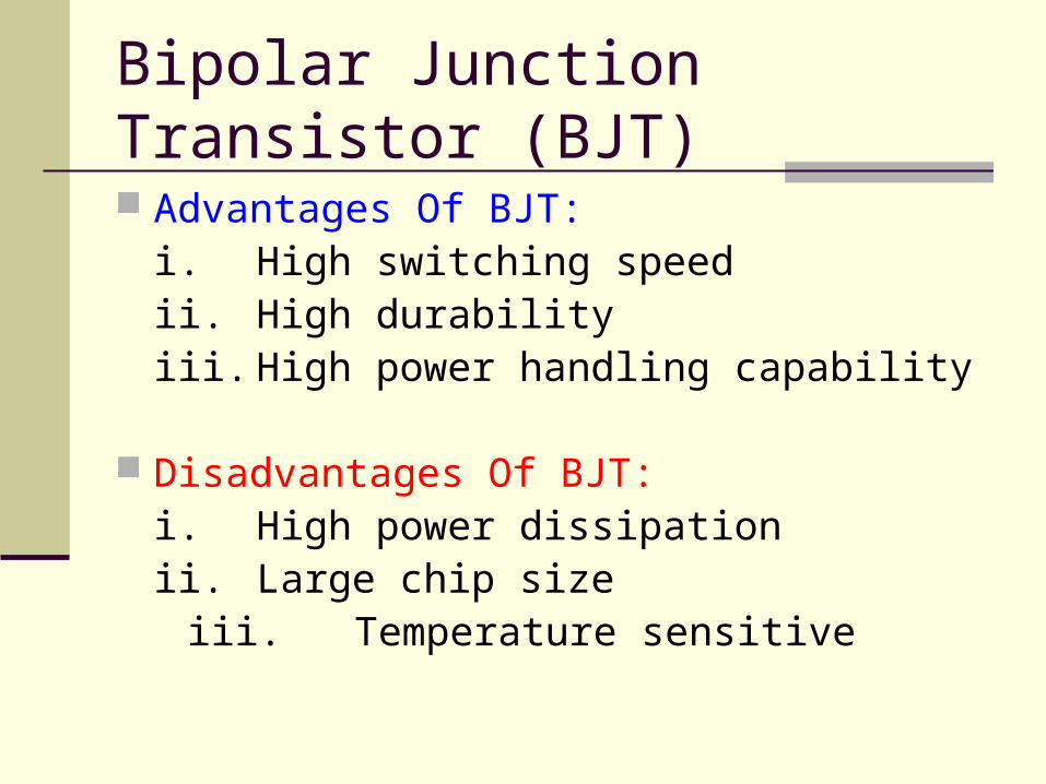
Bipolar Junction Transistor (BJT)
Advantages Of BJT:i. High switching speedii. High durabilityiii. High power handling capability
Disadvantages Of BJT:i. High power dissipationii. Large chip size
iii. Temperature sensitive
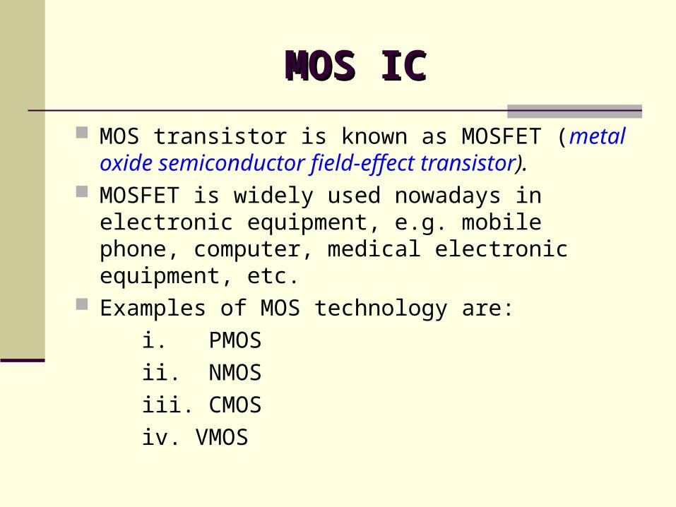
MOS ICMOS IC
MOS transistor is known as MOSFET (metal oxide semiconductor field-effect transistor).
MOSFET is widely used nowadays in electronic equipment, e.g. mobile phone, computer, medical electronic equipment, etc.
Examples of MOS technology are:
i. PMOS
ii. NMOS
iii. CMOS
iv. VMOS
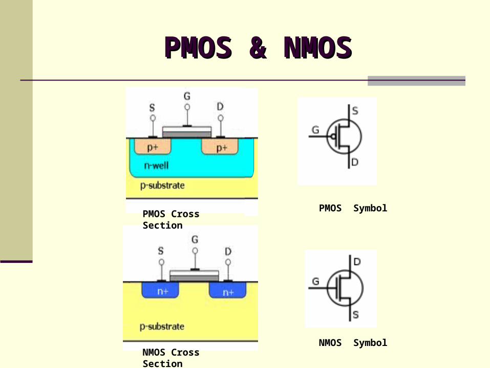
PMOS & NMOSPMOS & NMOS
PMOS Cross Section
NMOS Cross Section
PMOS Symbol
NMOS Symbol
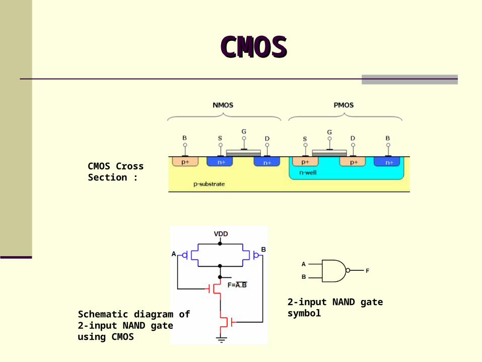
CMOSCMOS
CMOS Cross Section :
Schematic diagram of 2-input NAND gate using CMOS
2-input NAND gate symbol
VMOSVMOS
One of the disadvantages of CMOS technology is the disability of handling high power.
VMOS is invented to overcome the problem. VMOS has the capability to operate in high current and voltage.
VMOSVMOS
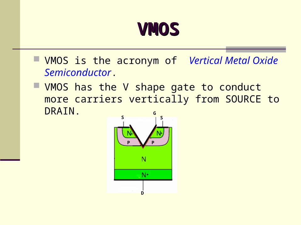
VMOS is the acronym of Vertical Metal Oxide Semiconductor.
VMOS has the V shape gate to conduct more carriers vertically from SOURCE to DRAIN.
P P
+
+
+
GS S
D
BiCMOSBiCMOS
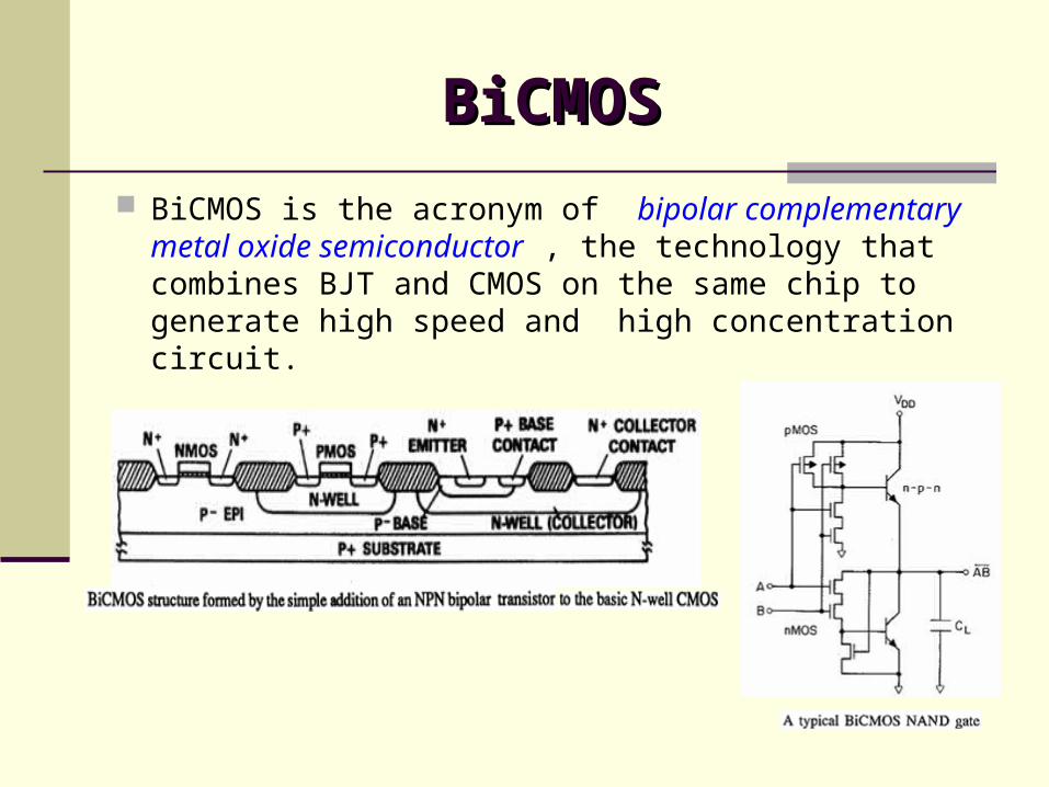
BiCMOS is the acronym of bipolar complementary metal oxide semiconductor , the technology that combines BJT and CMOS on the same chip to generate high speed and high concentration circuit.
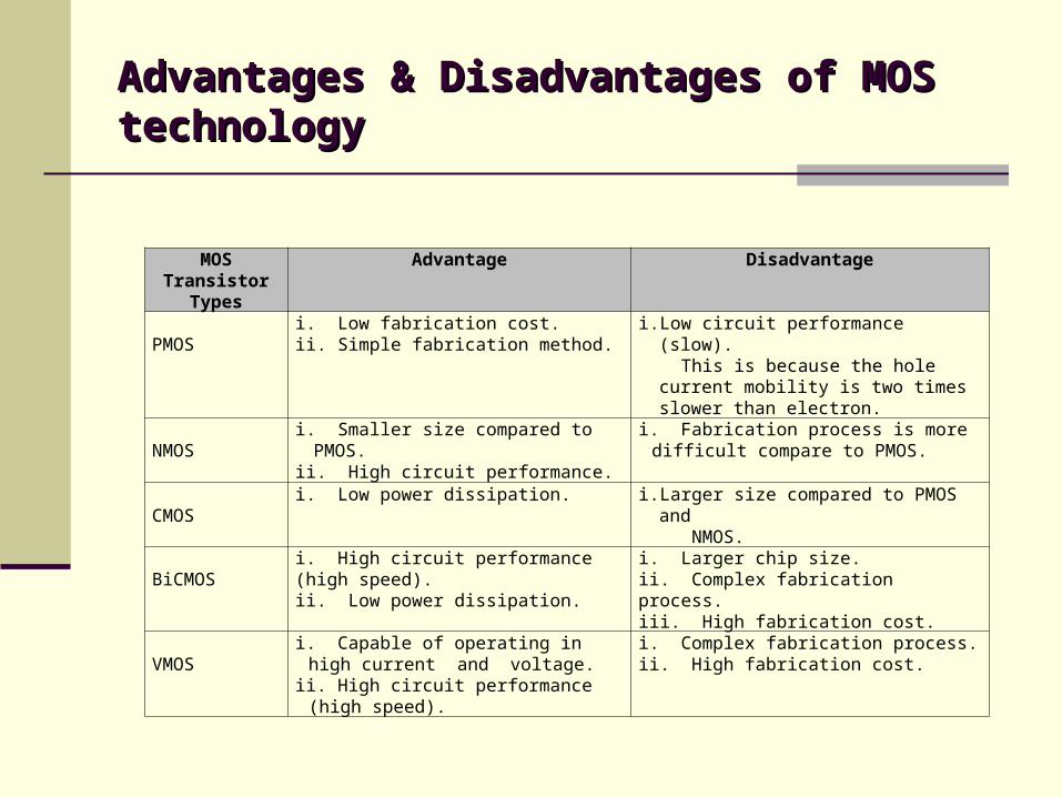
Advantages & Disadvantages of MOS technologyAdvantages & Disadvantages of MOS technology
MOS Transistor
Types
Advantage Disadvantage
PMOSi. Low fabrication cost.ii. Simple fabrication method.
i. Low circuit performance (slow). This is because the hole current
mobility is two times slower than electron.
NMOSi. Smaller size compared to PMOS.ii. High circuit performance.
i. Fabrication process is more difficult compare to PMOS.
CMOSi. Low power dissipation. i. Larger size compared to PMOS and
NMOS.
BiCMOSi. High circuit performance (high speed).ii. Low power dissipation.
i. Larger chip size.ii. Complex fabrication process.iii. High fabrication cost.
VMOSi. Capable of operating in high
current and voltage.ii. High circuit performance (high
speed).
i. Complex fabrication process.ii. High fabrication cost.

Classification Based on Circuits FunctionClassification Based on Circuits Function
Integrated Circuit
Linear / AnalogIntegrated circuits that operate with analogue signal at the input and output -continuous sine wave signal .Examples:i. Op-Ampii. Power Amplifieriii. Multiplieriv. Comparatorv. Voltage Regulator
DigitalIntegrated circuits that operate with digital signal at the input and output – Discrete square wave signal Examples:i. Logic gatesii. Flip-flopiii. Counteriv. Calculator chipsv. Memoryvi. Microprocessor
Analog and Digital ICAnalog and Digital IC


