Two types of challenging thin-film optical filter thatare of practical interest for dense wavelength-division multiplexing �DWDM� were devised for theoptical filter design contest held in conjunction withthe Topical Meeting on Optical Interference Coatings�OIC’2001�: They are a gain-flattening filter �GFF�and a DWDM filter with low pulse distortion at highbit rates.
For all designs in this contest we assumed
• An incidence medium of air �n0 � 1.0� and asubstrate of glass �ns � 1.52, back side perfectly an-tireflection coated�.
• Normal light incidence �� � 0�. �When a re-flective phase compensator was used for the secondproblem �DWDM�, normal incidence was also as-sumed for the reflector�.
A. Thelen’s �[email protected]� address is Rosskopfstrasse 13,60439 Frankfurt�Main, Germany. M. Tilsch �[email protected]� is with JDS Uniphase, Santa Rosa, California 95407.A. V. Tikhonravov �[email protected]� and M. K. Trubetskov�[email protected]� are with the Research Computing Cen-ter, Moscow State University, 119899, Moscow, Russia. U.Braunek �[email protected]� is with Schott Glaswerke, 55122 Mainz,Germany.
Received 11 October 2001; revised manuscript received 11 De-cember 2001.
• Perfectly homogeneous and nonabsorbing coat-ing materials, SiO2 �nL � 1.465� and Ta2O5 �nH �2.065�.
• Individual layers, each with a physical thick-ness greater than 10 nm.
• Total physical thickness less than 100 �m.• Number of layers fewer than 200.
A. Gain-Flattening Filter
Erbium-doped fiber amplifiers �EDFAs� are key ele-ments in fiber optic networks. Because their gain ishighly wavelength dependent, it is necessary toequalize the spectrum by cascading the EDFA with aGFF such that the ensemble has a flat gain spectrum.From packaging and reliability standpoints it is de-sirable to use a single filter for this operation.
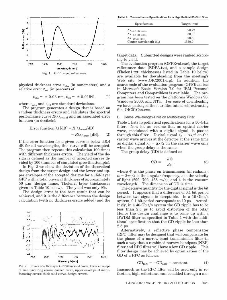
In Fig. 1 the target reflectance to be achieved by theGFF reflection filter for this contest is shown. Onedesign approach to meeting this specification was dis-cussed by Tilsch et al.1 With a high number of lay-ers �all of which can have different thicknesses� anda high total physical thickness, an almost perfectmatch to the target can be achieved. However, com-plex designs are generally much more sensitive tounavoidable manufacturing errors and might be in-ferior to designs that do not provide so good a matchbut are less sensitive to manufacturing errors.
For purposes of judging the contest a computerprogram was developed that simulates the manufac-turing process to permit the robustness of the designs
to be estimated. We assumed a random absolute
physical thickness error εabs �in nanometers� and arelative error εrel �in percent� of
εabs � � 0.03 nm, εrel � � 0.015%, (1)
where εabs and εrel are standard deviations.The program generates a design that is based on
random thickness errors and calculates the spectralperformance curve R���actual and an associated errorfunction �in decibels�:
Error function��� �dB� � R���actual�dB�
R���target �dB�. (2)
If the error function for a given curve is below 0.4dB for all wavelengths, this curve will be accepted.The program then repeats this calculation 100 timeswith different thickness errors. The yield of the de-sign is defined as the number of accepted curves di-vided by 100 �number of simulated growth attempts�.
In Fig. 2 we show the deviation of the theoreticaldesign from the target design and the lower and up-per envelopes of the accepted designs for a 153-layerGFF with a total physical thickness of approximately50 �m �design name, Thelen2; layer thicknessesgiven in Table 10 below�. The yield was only 9%.
The design error is the best result that can beachieved, and it is the difference between the designcalculation �with no thickness errors added� and the
target data. Submitted designs were ranked accord-ing to yield.
The evaluation program �GFFEval.exe�, the targetreflectance data �EDFA.txt�, and a sample design�Thelen1.txt; thicknesses listed in Table 10 below�are available for downloading from the meeting’sWeb site �www.OIC2001.org�. In addition, thesource code of the evaluation program �GFFEval.basin Microsoft Basic, Version 7.0 for IBM PersonalComputers and Compatibles� is available. The pro-gram has been tested on the platforms Windows 98,Windows 2000, and NT4. For ease of downloadingwe have packaged the four files into a self-extractingfile, OIC01Con.exe.
B. Dense Wavelength-Division Multiplexing Filter
Table 1 lists hypothetical specifications for a 50-GHzfilter. Now let us assume that an optical carrierwave, modulated with a digital signal, is passedthrough this filter. Digital signal �0 � ���2 on thecarrier wave arrives at the detector at the same timeas digital signal �0 ���2 on the carrier wave onlywhen the group delay is the same.
The group delay �GD� is defined as
GD � �d
d�, (3)
where is the phase on transmission �in radians�,� � 2�c�� is the angular frequency, c is the velocityof light �299, 792, 458 m�s�, and � is the vacuumwavelength. The dimension of GD is time.
The decisive quantity for the digital signal is the bitperiod. It appears that a difference of 0.1 bit periodbetween two signals is acceptable. In a 10-Gbit�ssystem, 0.1 bit period corresponds to 10 ps. Accord-ingly, in a 40-Gbit�s system the GD ripple has to beless than 2.5 ps to avoid distortion of the bits.2Hence the design challenge is to come up with aDWDM filter as specified in Table 1 with the addi-tional specification that the GD ripple be less than2.5 ps.
Alternatively, a reflective phase compensator�RPC� filter may be designed that will compensate forthe phase of a narrow-band transmission filter insuch a way that a combined narrow-bandpass �NBP�filter and RPC filter will have a low GD ripple. Thisfilter design may be achieved by optimization of theGD of a RPC as follows:
GDRPC � GDNBP � constant. (4)
Inasmuch as the RPC filter will be used only in re-flection, high reflectance can be added through a me-
Table 1. Transmittance Specifications for a Hypothetical 50-GHz Filter
Specification Target �nm�
��0.5 dB �90%� �0.22��3.0 dB �50%� �0.3��20 dB �1%� �0.6Center wavelength ��0� 1550.0
Fig. 1. GFF target reflectance.
Fig. 2. Errors of a 153-layer GFF �thin solid curve, lower envelopeof manufacturing errors; dashed curve, upper envelope of manu-facturing errors; thick solid curve, design errors�.
tallic base layer. So, in addition to the materialslisted above, gold �n � 0.36–10.4i� or silver �n �0.45–9i� may also be used for the RPC filter.
Figure 3 gives the GD of a classical NBP design3
�1.52��HL�10 HHLLL �HL�20 LLH �HL�21 H �HL�10
0.59525H 0.73669L�1�, where H is high and L is low,which meets the specifications listed in Table 1. Ascan be seen from the figure, the variation of the GD of
this classical design over the passband is 10.5 ps,which is not acceptable for a 40-Gbits optical net-work.
For this DWDM design problem, three types ofsubmission were solicited:
• A stand-alone NBP filter that meets the trans-mittance specification of Table 1 and has a signifi-cantly lower GD ripple in the passband than 9 ps �i.e.�5 ps� �Type NBP�.
• An NBP filter that meets the transmittancespecification of Table 1 �which has a GD ripple that iseasier to compensate for than the ripple in the designof Fig. 3� plus an RPC filter that reduces the GDripple in the passband to values below 2.5 ps �TypeNBP � RPC�.
• An RPC filter that reduces the GD ripple of thedesign given in Fig. 3 to less than 2.5 ps across thepass band �Type RPC�.
Submitted designs were ranked according to amountof GD ripple.
2. Results with Gain-Flattening Filters
Table 2 lists the names and addresses of all contrib-utors of GFF designs. Two contest team members,Alfred Thelen, Rosskopfstrasse 13, D-60439 Frank-furt�Main, Germany �[email protected]� and Al-
Table 2. Names and Addresses of Contributors of GFF Designs
Name Address E-Mail Address
Reuven Dahan Kidron 2 Zur-Yigal 44862 Israel [email protected] D. Noe Software Spectra, Inc., 14025 NW Harvest Lane,
exander Tikhonravov �Research Computing Center,Moscow State University, 119899 Moscow, Russia�[email protected]� submitted additional GFF de-signs. These team members’ designs were submit-ted on a no-contest basis, which means that theycould not win the contest.
Table 3 lists the yield, total physical thickness, andnumber of layers of all submitted GFF designs. Itcame as a big surprise to the design team that thespread in yield among the submitted designs was solarge for a product that is now in production at sev-eral thin-film manufacturing companies.
Pierre Verly was the clear winner of the GFF partof this contest. His design approach was publishedas a postdeadline paper4 at the conference and ispublished in this issue of Applied Optics. The reflec-tance of his design is shown in Fig. 4.
In what follows, we attempt to draw more conclu-sions that we believe will have considerable relevanceto thin-film technology.
A. Performance of the Gain-Flattening Filters withoutManufacturing Errors
In Table 4 the designs are ranked according to meritfunction and maximum width of the error corridor �indecibels�, assuming zero manufacturing errors �as de-termined with the GFFEval program�. The designThelen2, with a manufacturing yield of 9%, wasjudged to have the best merit function. The meritfunction of the winning design, Verly, with manufac-turing yield 98%, is worse by a factor of 2, and thedesign Noe, with a manufacturing yield of 76%, iseven worse by a factor of 3. Thus it can be concludedthat designing for a good merit function alone is notthe best way to design for maximum manufacturingyield.
B. Rankings of Designs with Different Errors and ErrorCombinations
In Tables 5–7 the designs are ranked according toyield �as determined with the GFFEval program� forvarious error combinations. For Table 5 both errors
ε were assumed to be doubled �εabs � 0.06 nm εrel �0.03%�, for Table 6 the absolute errors were in-creased and the relative errors were assumed to bezero �εabs � 0.2 nm εrel � 0%�, and for Table 7 theabsolute errors were assumed to be zero and the rel-ative errors were left unchanged �εabs � 0 nm εrel �0.03%�. If we now compare the ranking of Tables5–7 with the the ranking in the first column of Table3 we find that for doubling both errors �Table 5� theranking changed only slightly, for doubled absoluteerrors and no relative errors �Table 6� a significantchange in the ranking occurred �Thome was number8 in Table 5 and is now number 1�, and for relative
Table 4. GFF Designs Ranked According to Merit Function andMaximum Width Error Corridor �dB�, Assuming Zero Errors
errors only �Table 7� the ranking changed onlyslightly.
C. Philosophies for the Design of Gain-Flattening Filters
1. Error FlatteningThe design Thelen 2 was derived by standard de-
sign techniques including needle and gradual evolu-tion techniques, until no further improvement of themerit function was possible. An error analysis of thedesign is shown in Fig. 2. The theoretical error func-
tion oscillates from �0.15 to 0.15 dB. Feedingback a scaled error function as weights of the targetand further refining led to the design Thelen 1, whichhas almost twice the manufacturing yield.
2. Fourier-Transform Design MethodAccording to Tikhonravov,5 the ratio of reflectance
and transmittance can be represented in the form ofa Fourier-transform integral of the following type:
R�k�
T�k�� �
2TOTH
2TOTH
F�t�exp�ikt�dT, (5)
where k is the wave number and TOTH is the totaloptical thickness of the design. As a consequence,the Fourier transform of R�T differs from zero only inthe interval �2TOTH, 2TOTH�, which is specified bythe total optical thickness of the coating.
If t is small, the corresponding Fourier harmonicwill be a slowly varying function of the spectral pa-rameter k. Yet the targets of the GFF exhibit con-siderable amounts of changes in a narrow spectralband, requiring fast-changing functions with respectto spectral parameter k. It follows that the totaloptical thickness �TOTh� is the most important de-sign parameter and should be as large as possible.
There are two ways to maximize TOTh: maximizethe total physical thickness �TPTh� or maximize theratio �Ratio HL� of the total optical thickness of thehigh-index layer to the total optical thickness of thelow-index layers �because high-index layers are, forthe same physical thickness, optically thicker thanlow-index layers�.
As we can see from Table 8, all designs have ratiosH�L larger than 1. An extreme case is the designSouthw2, with a ratio of almost 10. Yet there is nocorrelation between yield and total optical thickness.A possible explanation for this could be that the fea-tures of the target are not so fast changing as themaximum total physical thickness �TpTh� allows.Apparently, a total optical physical thickness of 50�m is good enough.
To verify this finding we compared the second de-rivatives of the design Thelen1 �best merit function,
Table 6. GFF Performance with Absolute Errors Only ��abs � �0.2nm�rel � �0%�
Table 8. Total Physical Thicknesses TpTh and Total Optical Thicknesses ToTh of All Layers, Total Optical Thicknesses of all High-Index Layers Hand All Low-Index Layers L, and Their Ratio
Design TpTh ��m� ToTh ��m� ToTh H ��m� ToTh L ��m� Ratio H�L
ToTh � 90.6 �m, low yield�, Verly �average meritfunction, ToTh � 151.5 �m, highest yield�, and Noe�poorest merit function, ToTh � 98.7 �m, good yield�.We found that the designs have, except at the edges,comparable smoothness. We concluded that for thisGFF it is not necessary to use the maximally allowedTpTh of 100�m to resolve details satisfactorily.
D. Selected Designs
In Table 9 we list the quarter-wave optical thick-nesses �QWOT� of seven designs at a design wave-length of 1550 nm. The first layer for all designs isa high-index layer.
E. Conclusions for Gain Flattening Filters
It appears that the parameter spaces for the meritfunctions with and without manufacturing errors arequite different. As a consequence, one should notfirst optimize a merit function without errors andthen adapt it to errors �Thelen 1�. An optimizationtechnique that would include error targets from thestart would be desirable.
3. Results with 50-GHz Dense Wavelength-DivisionMultiplex Filters
Seven designs for single NBP filters were submittedby four authors. These designs are also identified bytheir authors’ names. Tony D. Noe �Software Spec-tra, Inc., 14025 Northwest Harvest Lane, Portland,Ore. 27229 �[email protected]�� submitted two RPCsfor his bandpass filter; these designs are designatedRPC1 and RPC2 in this paper. The affiliations ofthe designers of NBP filters are listed in Table 10.Noe was the only contributor of a NBP RPC design.We did not receive any submission to compensate forthe GD of Alfred Thelen’s bandpass filter.
A. Single-Bandpass Filters
Table 11 lists key features of the single-bandpassfilters, and Fig. 5 shows their cross sections. Alldesigns except the non-quarter-wave designs of Verlyhave easily identifiable spacers. Some designerspreferred H, others L material in the spacers. The
Table 10. Names and Addresses of Contributors of NBP Designs
Name Address E-Mail Address
Jennifer D. T. Kruschwitz JK Consulting, 47 Rossiter Road, Rochester, N.Y. 14620 [email protected] B. Mauer 2842 Ridgeway Avenue, Rochester, N.Y. 14626 [email protected] D. Noe Software Spectra, Inc., 14025 NW Harvest Lane, Portland, Ore. 97229 [email protected] G. Verly National Research Council of Canada, Ottawa K1A OR6, Canada [email protected]
Table 11. Key Features of Contributed Single-Bandpass Filters
cavity order �thickness of the spacers� varied consid-erably among the designs.
Figure 6 shows the intensity transmission re-sponse of the filters. Their specifications are plot-ted. Only three of the seven designs, Kruschwitz,Mauer3, and Noe, meet the intensity requirements.The reason that the other four designs fail becomesclearer as we look at the GD performance of thedesigns. Figure 7 shows the GD responses of thefilters.
As we can see from Table 12 no contestant was ableto design a filter that met both the transmission in-tensity and the GD requirements. Of the three de-signs that meet the intensity specification, Noe’s isthe narrowest at 0.5 dB and the widest at 20 dB.
His design has the lowest GD ripple, at 7.4 ps. Al-though not all the contributions were quarter-wave,they seem to confirm the finding of Ref. 6 for thephase properties of all quarter-wave wavelength-division multiplex filters, which establishes an inte-gral relationship between the intensity behavior ofthe transmission shape and the phase response of anNBP filter to transmission with the claim that satis-factory shape and small variation in group delay arenot possible. Mauer and Verly submitted designsfor which they gave up on trying to meet the intensityrequirement to reduce the GD ripple of the filter.The Mauer2 design achieves 3.2-ps GD ripple in thepassband. However, the filter’s 3-dB bandwidth is0.35 nm, which is above the tolerable bandwidth of0.3 nm.
B. Bandpass Filter with Reflective Phase Compensation
Table 13 summarizes the evaluation of Noe’s designsrelative to the specifications. The performance ofthe single NBP filter is included for comparison.Both RPCs have good all-pass qualities. The reflec-tion over the considered communication channel isabove 99.99% for RPC1 and above 99% for RPC2.The bandwidth of the NBP filter alone compared withthose of the solutions with the RPCs in tandem ispractically identical. Therefore both RPC solutionsmeet the amplitude requirements. Adding the GDof the NBP filter and the RPCs results in ripples overthe passband of 1.5 ps for RPC1 and of 0.9 ps forRPC2. Both solutions are well below the 2.5 ps re-quired by the specification.
Tony D. Noe was the winner of the NBP design
Table 12. NBP Design Performance Relative to Specifications
Specified Value
Design
Target Kruschwitz Mauer1 Mauer2 Mauer3 Noe Verly1 Verly2
contest. His design approach is described else-where7 in this journal.
In Table 14 we show the QWOT of the seven nar-row bandpass filters at the design wavelength of 1550nm. In Table 15 we show the layer sequence forTony Noe’s RPCs. The first layer consists of 100 nmof silver in both cases. All other layers are specifiedin QWOT at the design wavelength of 1550 nm. Forboth designs the first dielectric layer �layer 2� is ahigh-index layer.
C. Jennifer Kruschwitz’s Design Methodology
There are many ways to design a thin-film opticalinterference filter. Some designs are more an artthan a science, especially when all layers have tohave a thickness that is a multiple of a quarter of thedesign wave’s thickness. For those designers wholike to tailor a so-called proven prototype design to anew specification, the contestant Jennifer Krus-chwitz8 has developed a remarkable systematicscheme, which she has allowed us to present in thispaper �Table 16�. She started with a 200-GHz pro-totype design published by E-Tek.9 Then she usedthe fact that multiples of the spacer layers, odd mul-tiples of quarter-wave-thick layers in the stacks, anda symmetrical increase in the number of layers doesnot affect the central transmittance but does decreasethe bandwidth. In a final step, the last layers, whichcan be monitored without turning point accuracy, arerefined for maximum smoothness.
4. Discussion of Results
Although the number of contributions to the contestwas not large, their quality was great. The two win-ners, Pierre Verly and Tony Noe, contributed, in theopinion of the design team, masterpieces of design inwhich they combined sophisticated theoretical rela-tionships with intricate nonstandard numerical pro-cedures and switched on the fly from one designmethod to the other while the ever-improving designwas emerging.
There are two fundamentally different ap-proaches to the design of optical interference filters:the electrical engineering top-down approach inwhich prototype designs are used and the opticalengineering bottom-up approach in which buildingblocks such as equivalent layers and buffer layersare used. In optics it was often possible �by use ofsecondary effects through unique refractive-indexcombinations, unequal thicknesses, inhomogeneousfilms, or slight absorption� to find solutions thatwere considered theoretically impossible at thetime �minus, i.e., a filter with only one stop bandfrom 0 � � � �,10 nonpolarizing edge filters at 45°light incidence,11 an edge filter with a sharper cutoffand greater rejection in the stop band,12 etc.�. Infact, even the design of optical narrow-band filtersis in practice based not on using multiple “quarter-wave stacks with a quarter-wave shift in its cen-ter”6 but on using equivalent-layers theory3,13 andnonequal layers.14 These designs are superior toso-called prototype designs.
The design problems of this contest were of the newfrontier type. That is, the purpose of the contest wasto find solutions for applications for which, at the timeof the contest’s conception, there were no solutions.
In electrical engineering, three types of filters aregenerally considered15: maximally flat in the pass-band �Butterworth�, equal ripples in the passbandor in the stop band �Tschebyscheff �, and equal rip-ples in the passband and in the stop band �Cauer�.Butterworth and Tschebyscheff filters can be trans-lated into thin-film combinations, Cauer filters cannot.3 So, even if it could be shown that only Cauerfilters permit compensation for GD variation,6 thiswould not a priori mean that an interference filtersolution is impossible.
Although it was clear to the design team from thestart that there were solutions that use combina-tions of narrow-band filters �NBP� and reflectivephase compensators �RPC�, it was also believed thata single-filter narrow-band filter with low GD vari-
ation might have been a good design component ifthe all-quarter-wave limitation were lifted. Nei-ther a theoretical study by some contest team mem-bers during the contest period16 nor the results ofthe contest verified this assumption. It is interest-ing to note, though, that the three single-filter so-lutions that met the transmittance part of thespecifications had a spread of GD variation of closeto 2:1.
5. Summary
1. There appears to be no standard design tech-nique for high manufacturing yield.
2. Gain-flattening filters designed for good meritfunction without consideration of manufacturing er-rors can have a manufacturing yield that is lower byas much as a factor of 5.
3. Gain-flattening filters designed for high yieldthat consider relative manufacturing errors do notautomatically also have high yield when absolutemanufacturing errors are considered.
4. An optimization technique that uses low layersensitivities as targets would be a desirable compo-nent in the design of gain-flattening filters.
5. No contestant was able to design a singlenarrow-band filter with both good transmission in-tensity shape and low group-delay ripple.
6. By using two interference filters in series, onein transmission and one in reflection, one can designa filter combination with both good transmission in-tensity shape and low group-delay ripple.
The design team is very grateful to all the contes-tants for contributing their designs. Special thanksgo to the contestant Jennifer Kuschwitz for allowing usalso to include her design scheme in this publication.
Our deep gratitude goes also to Brian T. Sullivan,Iridian Spectral Technologies, Ottawa, Onrario, Can-ada, the general chair of OIC’2001, and Ric P. Shim-shok, Southwall Technologies, Palo Alto, Calif., theprogram chair of OIC’2001, for making this contestpossible and for making essential contributions to itscontent and form.
We thank Gadi Lenz, Lucent Technologies, BellLabs, Murray Hill, N. J., and Franz X. Kartner, In-stitut fur Hochfrequenztechnik and Quanten-elektronik, University of Karlsruhe, Karlsruhe,Germany, for helping us to establish the acceptableGD ripple, and Igor Kochikov, Research ComputingCenter of Moscow State University, Moscow, for help-ing us to clarify computational issues.
References and Notes1. M. Tilsch, C. A. Hulse, K. D. Hendrix, and R. B. Sargent, “Design
and demonstration of a thin-film based gain equalization filterfor C-band EDFAs,” presented at the National Fiber Optic En-gineering Conference, Chicago, Ill., 26–30 September 1999.
2. G. Lenz, Lucent Technologies, Bell Labs, 610 Mountain Ave-nue, Murray Hill, N.J. 07974 �personal communication, Au-gust 2000�.
3. All elements of this design, including the use of three quarter-wave layers, were discussed in A. Thelen, Design of OpticalInterference Coating �McGraw-Hill, New York, 1989�, Table10.1, p. 208. This design does not meet the specification of
Table 1 for ��3.0 dB �50%� because of an error: The last twolayers had thicknesses 0.75075H and 0.48694L instead of thevalues published in the contest announcement and this paper.Changing the numbers of the last two layers brings the designinto specification but increases the variation of GD from 10.5 to12.7 ps.
4. P. G. Verly, “Design of a robust thin-film interference filter forEDFA gain equalization,” Appl. Opt. 41, xxx–xxx �2002�.
5. A. V. Tikhonravov, “Amplitude–phase properties of the spec-tral coefficients of laminar media,” USSR Comput. Math.Math. Phys. 25, 77–83 �1985�.
6. G. Lenz, B. J. Eggleton, C. R. Giles, C. K. Madsen, and R. E,Slusher, “Dispersive properties of optical filters for WDM sys-tems,” IEEE J Quantum Electron. 34, 1390–1403 �1998�.
7. T. D. Noe, “Design of reflective phase compensator filters fortelecommunications,” Appl. Opt. 41, 3183–3186 �2002�.
8. J. Krushwitz, JK Consulting, 47 Rossiter Road, Rochester,N.Y. 14620 �personal communication, June 2001�.
9. J. J. Pan, F. Q. Zhou, and M. Zhou, “High-performance filters fordense wavelength-division-multiplex fiber optic communica-tions,” presented at the Society of Vacuum Coaters’ 41st AnnualTechnical Conference, Boston, Mass., 18–23 April 1998.
10. W. H. Southwell, “Rugate index profile which suppressed allharmonic stopbands,” in Optical Interference Coatings, Vol. 6of 1988 OSA Technical Digest �Optical Society of America,Washington, D.C., 1988�, pp. 142–145
12. T. C. Chen, “Optimised design of odd-order optical lowpass andhighpass multiplayer filters by method of coefficient match-ing.” IEE Proc. J 135, 166–177 �1998�.
13. A. Thelen, “Equivalent layers in multilayer filters,” J. Opt. Soc.Am. 56, 1533–1538 �1966�.
14. A. Thelen, A. V. Tikhonravov, and M. K. Trubetskov, “Push-button technology in optical coating design: pro et contra,” inAdvances in Optical Interference Coatings, C. Amra and A.Macleod, eds., Proc. SPIE 3738, 210–220 �1999�.
15. E. A. Guillemin, Synthesis of Passive Networks �Wiley, NewYork, 1957�.
Table 16. Jennifer Kruschwitz’s Methology for the Design of an NBP
Location inStructure
E-TEKDesign
3HDesign
Modified 3Hand Increase
Layers DesignFurther 3HModification
SpacerModification
Optimized forBandpass
Ripple
First cavity �H L�6
H 6L H�L H�6
�3H L�6
3H 6L 3H�L 3H�6
�H L�6 �3H L�2
3H 6L 3H�L 3H�2 �L H�6
�H L�6 �3H L�2
H 6L 3H�L 3H�2 �L H�6
�H L�6 �3H L�2
H 8L 3H�L 3H�2 �L H�6
�H L�6 �3H L�2
H 8L 3H�L 3H�2 �L H�6
Second cavity L �H L�7
H 4L H�L H�7 L
L �3H L�7
3H 4L 3H�L 3H�7 L
L �H L�7 �3H L�2
3H 4L 3H�L 3H�2 �H L�7 L
L �H L�9
3H 4L 3H�L 3H� �H L�8 L
L �H L�9
3H 4L 3H�L 3H� �H L�8 L
L �H L�9
3H 4L 3H�L 3H� �H L�8 L
Third cavity �H L�7
H 6L H�L H�7
�3H L�7
3H 6L 3H�L 3H�7
�H L�7 �3H L�2
3H 6L 3H�3H L�2 �H L�7
�H L�8 �3H L�3H 6L 3H
�H L�9
�H L�8 �3H L�3H 8L 3H
�H L�9
�H L�8 �3H L�3H 8L 3H
�H L�9
Fourth cavity L�H L�6
H 8L H�L H�6 L
L �3H L�6
3H 8L 3H�L 3H�6 L
L �H L�6 3H L�2
3H 8L 3H�L 3H�2 �L H�6 L
L �H L�8
3H 8L 3H�L H�8 L
L �H L�8
3H 6L 3H�L H�8 L
L �H L�8
3H 6L 3H�L H�8 L
Bandpass Ripple H L H L H L H L H L 1.0079HSmoothing 0.9834LLayers 0.9741H
16. A. Thelen, A. V. Tikhonravov, M. K. Trubewtskov, and M. A.Kokarev, “Phase properties of WDM filters,” in Optical Inter-ference Coatings, A. A. Sawchock, ed., Vol. 63 of OSA Trends inOptics and Photonics Series �Optical Society of America,Washington, D.C., 2001�, paper WD5.
The OIC’2001 Design Contest team. Left to right: Alexander V.Tikhonravov, Ulf Brauneck, Alfred J. Thelen, and Markus Tilsch.