Selected Topics on FE Electronics for the Selected Topics on FE Electronics for the GERDA Phase II Ge detector readout C.M. Cattadori INFN MiB Conference on Low Radiation Techniques 2015 Seattle (WA) 18-20 March 2015
Transcript
Selected Topics on FE Electronics for theSelected Topics on FE Electronics for the GERDA Phase II Ge detector readout
C.M. CattadoriINFN MiB
Conference on Low Radiation Techniques 2015Seattle (WA) 18-20 March 2015
OutlineOutline• GERDA experiment.• GERDA II vs GERDA I FE architecture• GERDA II vs GERDA I FE architecture• The Substrates• Signal and HV LinesSignal and HV Lines
– Front End and HV Ribbon Cables– JFETs– Feedback Resistors
• Results achieved in GERDA commissioning runsP l ti• Parylene coating
• Background Budget• Conclusions• ConclusionsAll the measurements presented in this talk have been performed by the LNGS ICPMS and γ-ray screening teams. With their highly professional work, they provides
n al able informations abo t material contaminations allo ing to proceed in the
20-Mar-15 2C. Cattadori - LRT 2015 - Seattle (WA)
unvaluable informations about material contaminations, allowing to proceed in the selection of materials for the setup construction.
GERDA @ LNGS: Searches of 0νββ of 76Ge
8/09/2014 C.M.Cattadori – NOW 2014
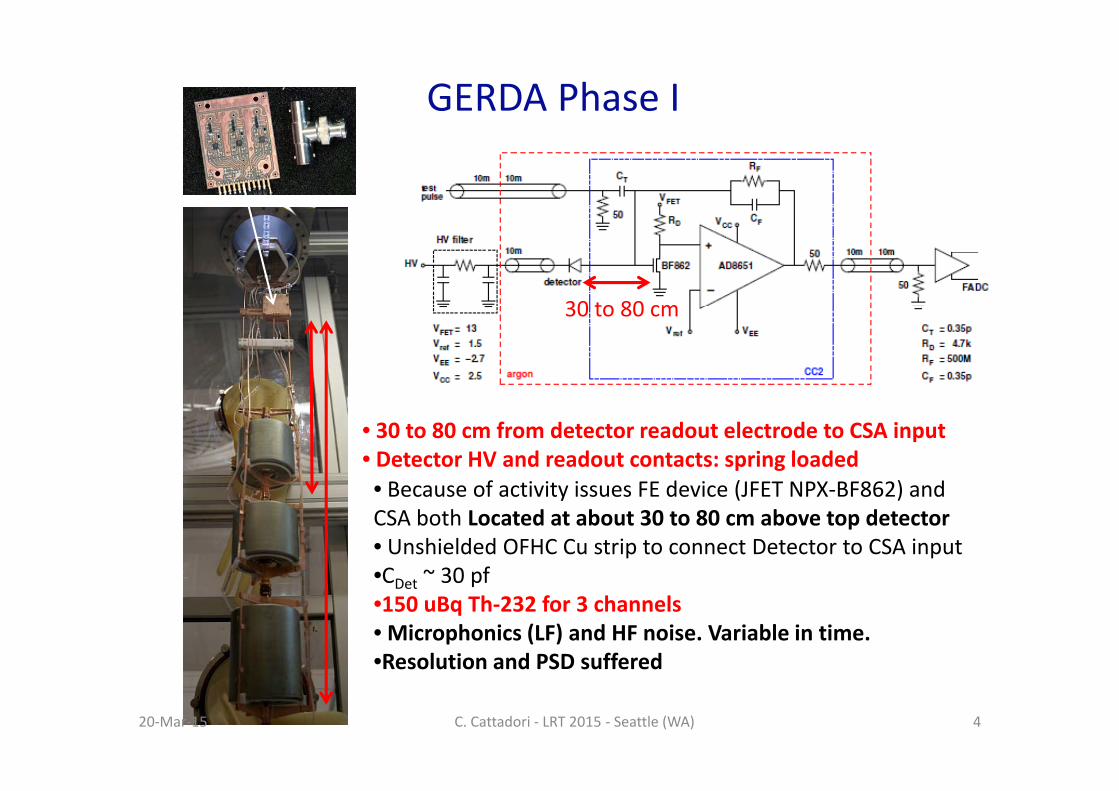
GERDA Phase I
30 to 80 cm30 to 80 cm
• Beca se of acti it iss es FE de ice (JFET NPX BF862) and
• 30 to 80 cm from detector readout electrode to CSA input• Detector HV and readout contacts: spring loaded• Because of activity issues FE device (JFET NPX-BF862) and CSA both Located at about 30 to 80 cm above top detector• Unshielded OFHC Cu strip to connect Detector to CSA input•C ~ 30 pf•CDet 30 pf•150 uBq Th-232 for 3 channels• Microphonics (LF) and HF noise. Variable in time.•Resolution and PSD sufferedResolution and PSD suffered
20-Mar-15 4C. Cattadori - LRT 2015 - Seattle (WA)
Detector Performancesimprovement by tailored DSPimprovement by tailored DSP
• Filtering with an improved filter, tailored foreach detector Improved 10% FWHM bothfor Coax and BEGE & stability of reconstructed
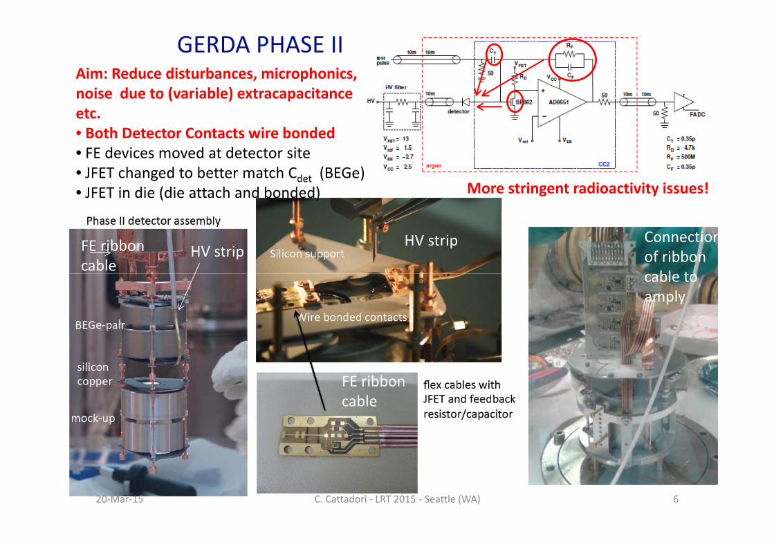
d ( bl )noise due to (variable) extracapacitanceetc.• Both Detector Contacts wire bonded
FE d i d t d t t it• FE devices moved at detector site• JFET changed to better match Cdet (BEGe)• JFET in die (die attach and bonded) More stringent radioactivity issues!
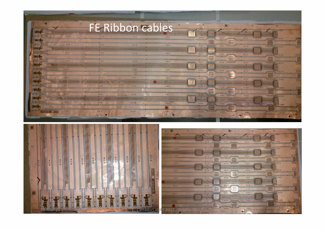
HV stripHV stripFE ribbon
cable
Connectionof ribbon
bl tcable toamply
FE ribbonblcable
20-Mar-15 6C. Cattadori - LRT 2015 - Seattle (WA)
Noise figure of a Canberra 2002 l fi F C b d t h t
20-Mar-15 7C. Cattadori - LRT 2015 - Seattle (WA)
amplyfier. From Canberra data sheet
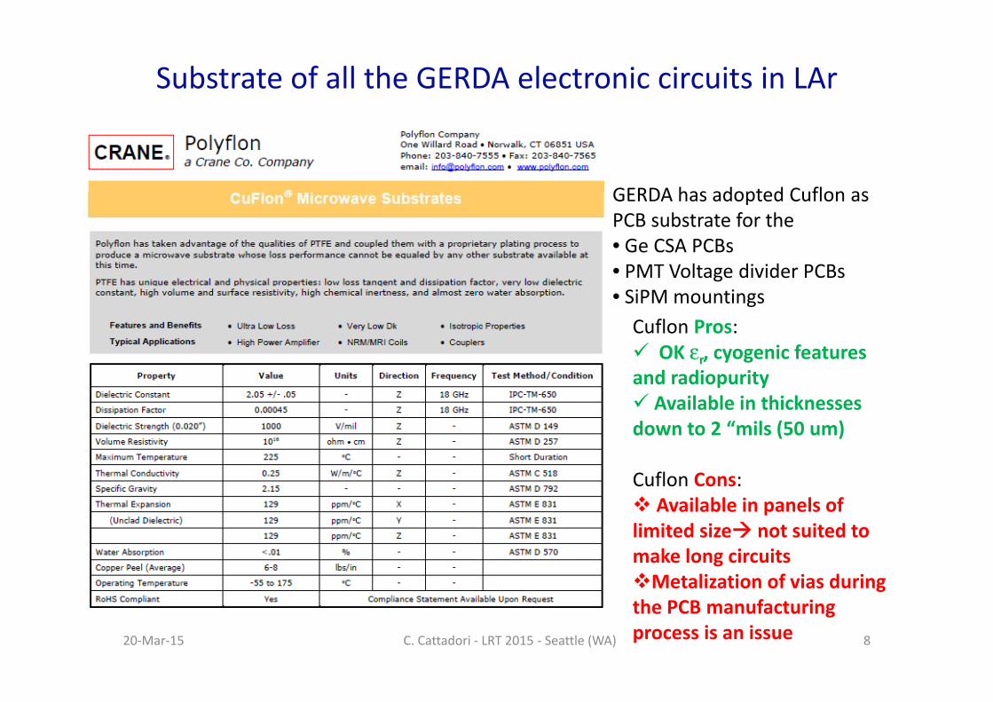
Substrate of all the GERDA electronic circuits in LAr
GERDA has adopted Cuflon asGERDA has adopted Cuflon asPCB substrate for the • Ge CSA PCBs• PMT Voltage divider PCBs• PMT Voltage divider PCBs• SiPM mountings
Cuflon Pros: OK ε cyogenic features OK εr, cyogenic featuresand radiopurity Available in thicknessesdown to 2 “mils (50 um)down to 2 mils (50 um)
Cuflon Cons: Available in panels of Available in panels oflimited size not suited tomake long circuitsMetalization of vias during
20-Mar-15 C. Cattadori - LRT 2015 - Seattle (WA) 8
gthe PCB manufacturing process is an issue
Typical activity valuesmeasured for Cuflon
i l h ICPMS dmaterial at the ICPMS and STELLA γ-screening facilities @ LNGS
Values can slightly changefollowing substrate thicknesses
d C /T fl f iand Cu/Teflon fraction
Cuflon cleaner than Kaptonfactor 15 in Ra 226factor 15 in Ra-226 factor 40 in U-238
20-Mar-15 C. Cattadori - LRT 2015 - Seattle (WA) 9
Features of FE Ribbon cables (Coplanar Waveguides)• Substrates :
– Cuflon 50-75 um : εr=2.1– Kapton 50-75 um: εr=3.4
h diff d• Lengths to connect different detectors toCSA:– 48 cm to 80 cm8 c to 80 c
IMPORTANT: Regular waveforms only if• Impedence properly matched
E t C i t d d b th l iti li
C
• Extra C introduced by the long capacitive linecompensated at the amplyfier relevant node• To preserve pulse rise time keep trace C as low as possible
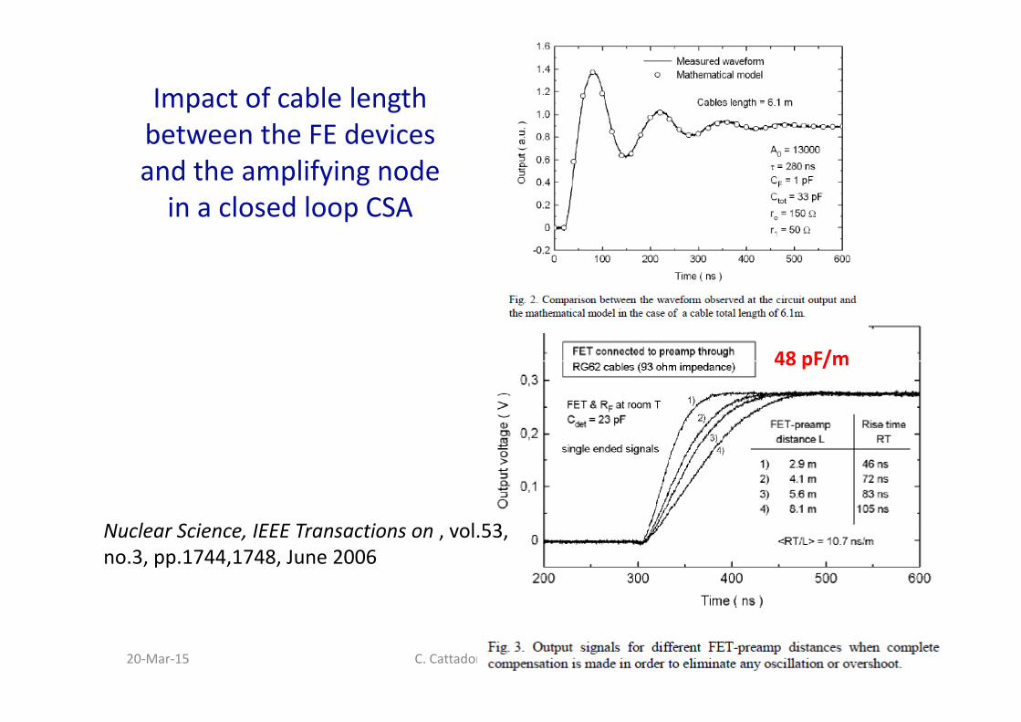
Impact of cable lengthbetween the FE devicesand the amplifying node
i l d l Sin a closed loop CSA
48 pF/m48 pF/m
N l S i IEEE T ti l 53Nuclear Science, IEEE Transactions on , vol.53, no.3, pp.1744,1748, June 2006
20-Mar-15 C. Cattadori - LRT 2015 - Seattle (WA) 11
Issues related to manufacturing long (up to80 cm) radiopure flex transmission lines80 cm) radiopure flex transmission lines
1° Find raw material radiopure, good εr, proper thickness, cryogenic etc.CuflonCaveat: Polyflon can produce panels 22” maximal lengthCaveat: Polyflon can produce panels 22 maximal length. 33” panels came in heavily defected and with poor adhesion of Cu to Teflon layer.2° Fi d th f t th t d h l fl i it b t lli2° Find the manufacturer that can produce such long flex circuit by controllingthe radioactivity introduced in the PCB process
Alternative material for long circuits: DuPont PyraluxDuPont Pyralux
From ICPMS & γ-screening: • once PCB processed Pyralux and Cuflon have about the same specific activity( f d b b h d )(confirmed by both ICPMS and γ-screening)• Kapton has (6 ± 1 )mBq/kg of Ra-226, not visible in ICPMS measurements, wellvisible in γ-screening
PYRALUX
CUFLON
Impact of PCB process on final FE circuits contaminations
• Once selected the proper raw material Important not to spoil its radiopurity byPCB process.p
• Avoid finishing protective layers (soldermasks etc.)• Minimize Cu deposition• Gold finishing required for bonding (typically <1 um ) introduces significant UGold finishing required for bonding (typically <1 um ) introduces significant U
contaminations. Minimize golded surfaces (in GERDA few mm2/detector)
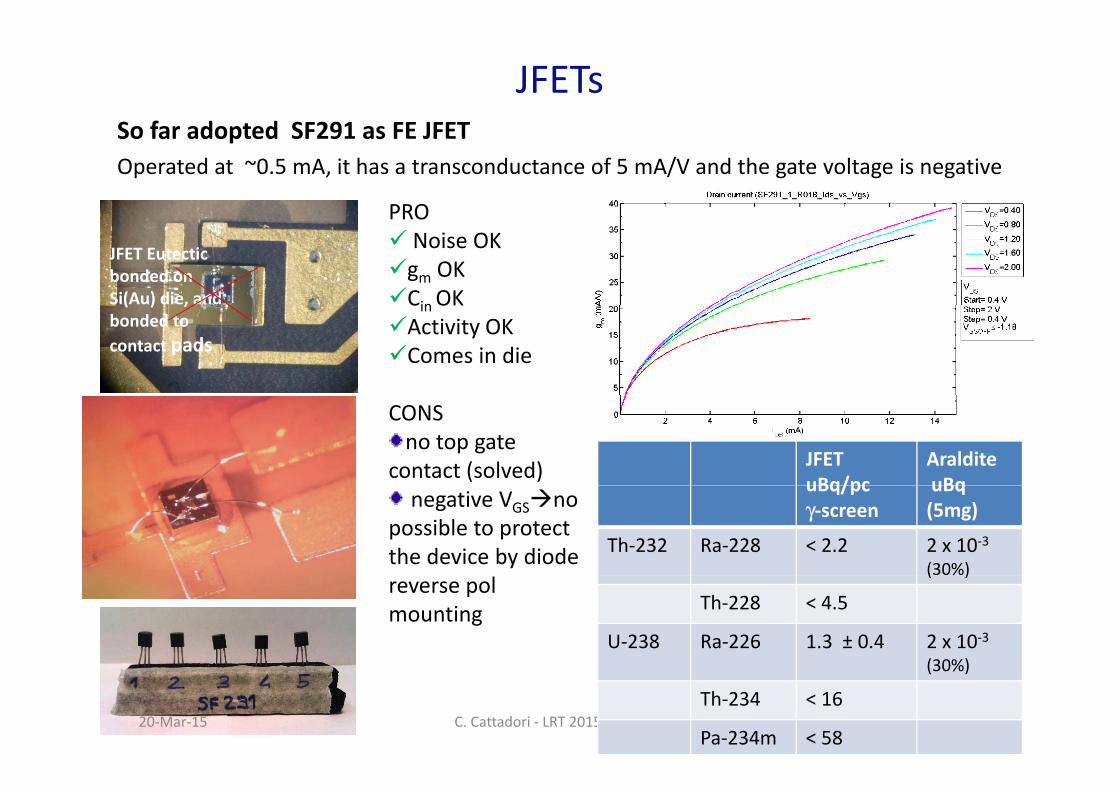
JFETsSo far adopted SF291 as FE JFETSo far adopted SF291 as FE JFETOperated at ~0.5 mA, it has a transconductance of 5 mA/V and the gate voltage is negative
PROPRO Noise OKgm OKCin OK
JFET Eutecticbonded on Si(Au) die, and in
Activity OKComes in die
( ) ,bonded tocontact pads
CONSno top gate
contact (solved) JFETuBq/pc
AralditeuBq
negative VGSno possible to protectthe device by diode
Th & Ra scale with Volume as expectedK lower than expected
BI w. veto 3.4E 5 3.4E 7
K lower than expectedPb-210 doesn't scale with volume probably from the contact pads
The activity of the R in 0402 size is within the expected activity of theThe activity of the R in 0402 size is within the expected activity of the Signal Flex cable
20-Mar-15 C. Cattadori - LRT 2015 - Seattle (WA) 22
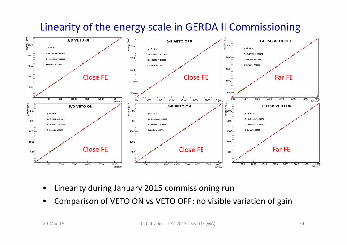
Close FE
l f h dTypical Performances achievedin GERDA Commissioning run Close FE
Close FE
20-Mar-15 C. Cattadori - LRT 2015 - Seattle (WA) 23Bstat= 2.352 x 2.96 eV x 0.13 =2.13 eV
Far FE
Linearity of the energy scale in GERDA II Commissioning
Close FE Close FE Far FE
Close FE Close FE Far FEClose FE Close FE Far FE
• Linearity during January 2015 commissioning run• Comparison of VETO ON vs VETO OFF: no visible variation of gain
20-Mar-15 C. Cattadori - LRT 2015 - Seattle (WA) 24
Typical survival fractions after pulse shapediscrimination in GERDA II Commissioning.
Double Escape Line(1592 keV) is proxy ofsingle side eventsCut of PSD defined tohave acceptance= 90% Bi-212 1620 keV line is
proxy of multi-siteeventsAcceptance of PSD:10-15%
Acceptance ofCompton continuum: ~ 50%
20-Mar-15 C. Cattadori - LRT 2015 - Seattle (WA) 25
20-Mar-15 C. Cattadori - LRT 2015 - Seattle (WA) 26
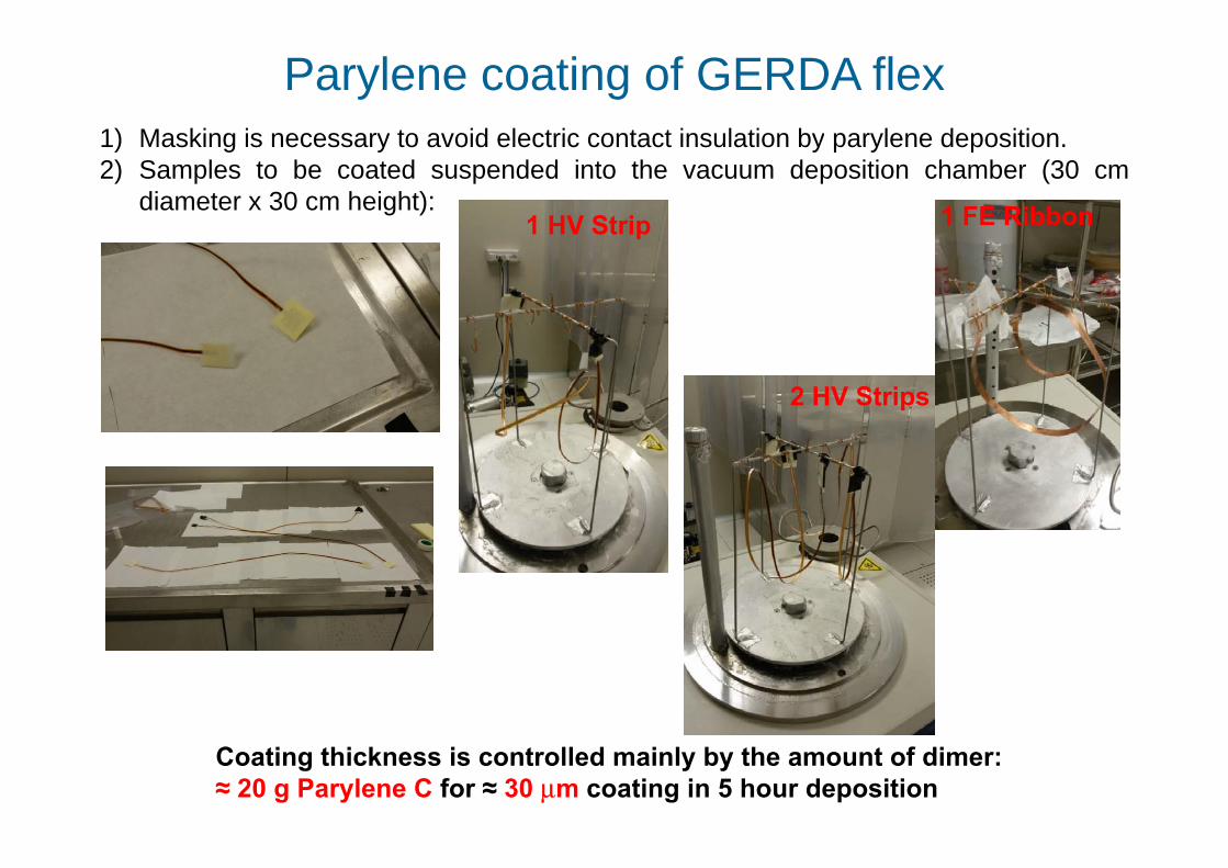
Flex circuit conformal coating:Parylene deposition system available @ LNGSy p y @
The PDS 2010 transforms Parylene dimer to a gaseous monomer; upon deposition the material polymerizes, at room temperature, onto the substrate. There is no intermediate liquid phase or separate cure cycle At the vacuumThere is no intermediate liquid phase or separate cure cycle. At the vacuum levels employed, all sides of the substrate are uniformly impinged by the gaseous monomer, resulting in a truly conformal coating.
Parylene coating of GERDA flex1) Masking is necessary to avoid electric contact insulation by parylene deposition1) Masking is necessary to avoid electric contact insulation by parylene deposition.2) Samples to be coated suspended into the vacuum deposition chamber (30 cm
diameter x 30 cm height):1 HV Strip 1 FE Ribbonp
2 HV Strips
Coating thickness is controlled mainly by the amount of dimer: ≈ 20 g Parylene C for ≈ 30 μm coating in 5 hour deposition
Radiopurity of Parylene C ICP-MS measurement @ LNGS:
Th U K Pb
GALXYL C < 40 ppt(<1.62*10-7 Bq/g)
< 20 ppt(<2.45*10-7
B / )
< 200 ppb(<26 Bq/g)
< 2 ppb
Bq/g)
For example1 GERDA Ph II unit= 2 BEGEs4 GERDA Ph II units 8 signal FLEXs
Estimated contamination due to 8 signal (or HV) cables
Araldite 5,0E-3 MS 1 2,20E-03 0,009 1,80E-03 0,005
Bronze Springs 1,2 MS 1 2,44E-01 30% 0,56 0,0016 3,0E-01 30% 0,4428 0,0583PTFE per detector pair 3 GA 1 9 0E-02 4% 0 21 0 0006 7 5E-02 3% 0 1125 0 0148pair 3 GA 1 9,0E-02 4% 0,21 0,0006 7,5E-02 3% 0,1125 0,0148Si per detector pair 40 GA 1 2,00E+01 46,00 0,1314 1,40E+01 21,0000 2,7632Cu per detector pair 26 GA 1 5,2E-01 1,20 0,0034 5,2E-01 0,7800 0,1026
mini shroud 17,4 MS 0,25 0,3 0,7 0,0021 0,62 0,9351 0,1230Limits
ConclusionsConclusions
• I th f k f th GERDA t d t th Ph II th• In the framework of the GERDA setup upgrade to the Phase II, the Ge-FE electronic has been upgraded to better match the Phase II detector features with the aim of preserving the Ge signals (54 fCfor 1 MeV released in Ge) from HF and LF disturbances andfor 1 MeV released in Ge) from HF and LF disturbances and minimizing the intrinsic noise related to long capacitive lines
• Designed and manufactured flex circuits to contact, by wire bondingthe Ge detectors and to act as substrates for the FE devices (JFET inthe Ge detectors and to act as substrates for the FE devices (JFET in die) and coplanar waveguides
• Results achieved are OK in term of Energy (FWHM 3 k V @ 2614 k V) d P l Sh l i– (FWHM < 3 keV @ 2614 keV) and Pulse Shape analysis ,
– not yet satisfactory in term of reliability of JFET survival fraction GERDA PHASE II will start with still far away front end devices
• Huge and systematic effort selecting the FE components (JFETs• Huge and systematic effort selecting the FE components (JFETs, SMD Resistors) and qualifying the PCB process has been done in collaboration with the LNGS facilities. This to reach GERDA Phase II design background index of 10-3 cts/(keV kg y) at Q (2039 keV)design background index of 10 cts/(keV kg y) at Qββ (2039 keV).
20-Mar-15 C. Cattadori - LRT 2015 - Seattle (WA) 31
EXTRA SLIDESEXTRA SLIDES
20-Mar-15 C. Cattadori - LRT 2015 - Seattle (WA) 32
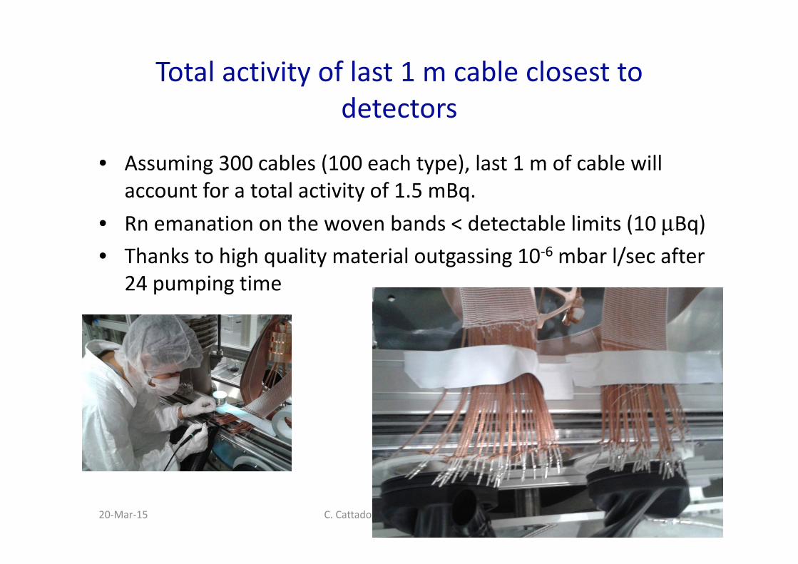
Total activity of last 1 m cable closest to detectors
• Assuming 300 cables (100 each type), last 1 m of cable will account for a total activity of 1.5 mBq.R ti th b d d t t bl li it (10 B )• Rn emanation on the woven bands < detectable limits (10 μBq)
• Thanks to high quality material outgassing 10-6 mbar l/sec after24 pumping time24 pumping time