Topology optimization of piezoelectric nanostructures S.S. Nanthakumar c , Tom Lahmer c , Xiaoying Zhuang d,g,n , Harold S. Park e,n , Timon Rabczuk a,b,c,f,nn a Division of Computational Mechanics, Ton Duc Thang University, Ho Chi Minh City, Viet Nam b Faculty of Civil Engineering, Ton Duc Thang University, Ho Chi Minh City, Viet Nam c Institute of Structural Mechanics, Bauhaus-University Weimar, Marienstr.15, D-99423 Weimar, Germany d Department of Geotechnical Engineering, Tongji University, Shanghai, China e Department of Mechanical Engineering, Boston University, 730 Commonwealth Avenue, ENA 212, Boston, MA 02215, United States f School of Civil, Environmental and Architectural Engineering, Korea University, Seoul, Republic of Korea g Institute of Continuum Mechanics, Leibniz University Hannover, AppelStr.11, D-30167 Hannover article info Article history: Received 20 November 2015 Received in revised form 25 February 2016 Accepted 9 March 2016 Available online 12 May 2016 Keywords: ZnO nanostructures Surface piezoelectricity Surface elasticity Topology optimization abstract We present an extended finite element formulation for piezoelectric nanobeams and nanoplates that is coupled with topology optimization to study the energy harvesting potential of piezoelectric nanostructures. The finite element model for the nanoplates is based on the Kirchoff plate model, with a linear through the thickness distribution of electric potential. Based on the topology optimization, the largest enhancements in energy harvesting are found for closed circuit boundary conditions, though significant gains are also found for open circuit boundary conditions. Most interestingly, our results demon- strate the competition between surface elasticity, which reduces the energy conversion efficiency, and surface piezoelectricity, which enhances the energy conversion efficiency, in governing the energy harvesting potential of piezoelectric nanostructures. & 2016 Elsevier Ltd. All rights reserved. 1. Introduction Piezoelectric energy harvesters have garnered significant attention because of their ability to convert ambient me- chanical energy into electrical energy (Priya, 2009, 2007). These energy harvesters have been utilized in a wide range of applications, where a review of vibration based energy harvesters is presented in Sodano et al. (2004). Because of their wide usage, approaches to design piezoelectric energy harvesters with higher energy conversion effi- ciency have also been developed. One such approach is using computational topology optimization, where the geometry of the energy harvesters can be tuned to maximize the energy conversion efficiency. Examples of using topology optimization to design superior piezoelectric energy harvesters abound, including maximizing electromechanical conversion for a certain vibration mode (Silva and Kikuchi, 2007), designing a layout comprising the energy harvester as well as the electrical circuit (Rupp et al., 2009), and maximizing the energy conversion factor in cantilever plate energy harvesters subject to static loads (Zheng et al., 2009). There have also been works performing topology optimization of energy harvesters using different design variables, for example the densities that define the presence of piezoelectric material in each finite element Contents lists available at ScienceDirect journal homepage: www.elsevier.com/locate/jmps Journal of the Mechanics and Physics of Solids http://dx.doi.org/10.1016/j.jmps.2016.03.027 0022-5096/& 2016 Elsevier Ltd. All rights reserved. n Corresponding authors. nn Corresponding author at: Institute of Structural Mechanics, Bauhaus-University Weimar, Marienstr.15, D-99423 Weimar, Germany. E-mail addresses: [email protected](X. Zhuang), [email protected](H.S. Park), [email protected](T. Rabczuk). Journal of the Mechanics and Physics of Solids 94 (2016) 316–335
Transcript
Contents lists available at ScienceDirect
Journal of the Mechanics and Physics of Solids
Journal of the Mechanics and Physics of Solids 94 (2016) 316–335
http://d0022-50
n Corrnn CorE-m
journal homepage: www.elsevier.com/locate/jmps
Topology optimization of piezoelectric nanostructures
S.S. Nanthakumar c, Tom Lahmer c, Xiaoying Zhuang d,g,n, Harold S. Park e,n,Timon Rabczuk a,b,c,f,nn
a Division of Computational Mechanics, Ton Duc Thang University, Ho Chi Minh City, Viet Namb Faculty of Civil Engineering, Ton Duc Thang University, Ho Chi Minh City, Viet Namc Institute of Structural Mechanics, Bauhaus-University Weimar, Marienstr. 15, D-99423 Weimar, Germanyd Department of Geotechnical Engineering, Tongji University, Shanghai, Chinae Department of Mechanical Engineering, Boston University, 730 Commonwealth Avenue, ENA 212, Boston, MA 02215, United Statesf School of Civil, Environmental and Architectural Engineering, Korea University, Seoul, Republic of Koreag Institute of Continuum Mechanics, Leibniz University Hannover, AppelStr. 11, D-30167 Hannover
a r t i c l e i n f o
Article history:Received 20 November 2015Received in revised form25 February 2016Accepted 9 March 2016Available online 12 May 2016
x.doi.org/10.1016/j.jmps.2016.03.02796/& 2016 Elsevier Ltd. All rights reserved.
esponding authors.responding author at: Institute of Structuralail addresses: [email protected] (X
a b s t r a c t
We present an extended finite element formulation for piezoelectric nanobeams andnanoplates that is coupled with topology optimization to study the energy harvestingpotential of piezoelectric nanostructures. The finite element model for the nanoplates isbased on the Kirchoff plate model, with a linear through the thickness distribution ofelectric potential. Based on the topology optimization, the largest enhancements in energyharvesting are found for closed circuit boundary conditions, though significant gains arealso found for open circuit boundary conditions. Most interestingly, our results demon-strate the competition between surface elasticity, which reduces the energy conversionefficiency, and surface piezoelectricity, which enhances the energy conversion efficiency,in governing the energy harvesting potential of piezoelectric nanostructures.
& 2016 Elsevier Ltd. All rights reserved.
1. Introduction
Piezoelectric energy harvesters have garnered significant attention because of their ability to convert ambient me-chanical energy into electrical energy (Priya, 2009, 2007). These energy harvesters have been utilized in a wide range ofapplications, where a review of vibration based energy harvesters is presented in Sodano et al. (2004).
Because of their wide usage, approaches to design piezoelectric energy harvesters with higher energy conversion effi-ciency have also been developed. One such approach is using computational topology optimization, where the geometry ofthe energy harvesters can be tuned to maximize the energy conversion efficiency. Examples of using topology optimizationto design superior piezoelectric energy harvesters abound, including maximizing electromechanical conversion for a certainvibration mode (Silva and Kikuchi, 2007), designing a layout comprising the energy harvester as well as the electrical circuit(Rupp et al., 2009), and maximizing the energy conversion factor in cantilever plate energy harvesters subject to static loads(Zheng et al., 2009). There have also been works performing topology optimization of energy harvesters using differentdesign variables, for example the densities that define the presence of piezoelectric material in each finite element
S.S. Nanthakumar et al. / J. Mech. Phys. Solids 94 (2016) 316–335 317
(Nakasone and Silva, 2009), or the geometry of elastic substructure (Wein et al., 2013). In Chen et al. (2010), an approach fordesigning the optimal configuration of a cantilever and a cylindrical piezoelectric energy harvesters with single and multiplematerials was presented. A procedure for converting an inverse problem of detecting flaws in piezoelectric structures intoan iterative optimization problem was given in Nanthakumar et al. (2013, 2014, 2016).
However, most piezoelectric energy harvesters have been developed using bulk materials. The exciting possibility ofusing nanoscale piezoelectric energy harvesters emerged in 2006 with the discovery of piezoelectricity from ZnO nanowiresby Wang and Song (2006). Many researchers have since extended the original seminal work, including the development ofself-powered nano generators that can provide gate voltage to effectively control charge transport (Wang and Song, 2006),lateral and vertical integration of ZnO nanowires into arrays that are capable of producing sufficient power to operate realdevices (Xu et al., 2010), and the experimental determination that the piezoelectric coefficient d33 of ZnO nanobelt is muchlarger compared to bulk ZnO through measurements made using piezoresponse force microscope (Zhao et al., 2004). Arecent review on the electromechanical properties and performance of ZnO, and other piezoelectric nanostructures, wasperformed by Espinosa et al. (2012).
Along with experimental work, there have been some recent theoretical studies into the piezoelectric properties ofnanostructures and nanowires. Dai et al. (2011) highlighted the concept of surface piezoelectricity using a combination oftheory and atomistic calculations, and then analyzed the (0001) surfaces of ZnO. Other works have also found that ZnOnanostructures exhibit different piezoelectric properties as compared to bulk ZnO (Mitrushchenkov et al., 2009; Momeniet al., 2012a), while surface effects on the piezoelectricity of ZnO nanowires were studied by Dai and Park (2013). Usingquantummechanical calculations, Agrawal and Espinosa (2011) found substantial increases in the piezoelectric properties ofZnO and GaN nanowires with decreasing size, while an increase of piezoelectric coefficient to 2.322 C/m2 compared to abulk value of 1.4 C/m2 when the nanobelt thickness decreases to 0.8 nmwas obtained using a molecular dynamics model byMomeni et al. (2012b).
Other researchers have developed analytic models for surface elasticity and surface piezoelectricity. For surface elasticity,the seminal work was that of Gurtin, Murdoch and co-workers (Gurtin and Murdoch, 1975; Gurtin et al., 1998), who werethe first to establish a surface or interface elasticity model to capture surface stress and elastic effects. The elastic propertiesof nanostructures with surface and interface effects using the extended finite element method (XFEM) were proposed byYvonnet et al. (2008), and later extended by Farsad et al. (2010) to study the mechanical behavior of homogeneous andcomposite nanobeams. For surface piezoelectricity, various analytic models have been developed, including an explicitformula for the electromechanical coupling coefficient considering surface effects (Yan and Jiang, 2011a) for piezoelectricnanowires, an Euler–Bernoulli beam theory for the vibrational and buckling behavior of piezoelectric nanobeams (Yan andJiang, 2011b), and the electroelastic response of thin piezoelectric places considering surface effects using Kirchoff platetheory (Wang, 2012). It is also worth emphasizing that the electromechanical coupling, and nanoscale piezoelectricity,should also be impacted by surface elastic effects, as experiments have shown that ZnO nanowires with diameter smallerthan about 100 nm exhibit a dramatic increase in elastic modulus as compared to bulk ZnO (Chen et al., 2006).
The objective of this work is to develop and apply topology optimization techniques to study how surface electro-mechanical effects impact the energy conversion efficiency of piezoelectric ZnO nanostructures. We accomplish this bydiscretizing the equations of surface piezoelectricity using the extended finite element method (XFEM), and using thisnumerical formulation to study energy harvesting from piezoelectric nanowires, nanoplates, and piezoelectric layers inenergy harvesters accounting for both surface elastic and surface piezoelectric effects. Our results demonstrate the relativeeffects of both surface elasticity and piezoelectricity on the electromechanical energy conversion efficiency, while alsoelucidating the difference in performance of the nanoscale energy converters under both open and closed circuit boundaryconditions.
2. Governing equations of surface piezoelectricity
We consider a piezoelectric domain Ω with a material surface Γ. Based on the continuum theory of surface piezo-electricity (Dai et al., 2011), the equilibrium equations are
σ∇ Ω· + = ( )b 0 in 1
∇ Ω· − = ( )qD 0 in 2
σ∇ Γ· = ( )0 on 3s s
∇ Γ· = ( )D 0 on 4s s
where σ and D are mechanical stress and electric displacement, respectively, while σs and Ds are the surface stress and thesurface electric displacement, respectively. In the above equation, σ σ∇ ∇· = P:s s and ∇ ∇· =D D P:s s where : is the doubletensor contraction and where P is a second order tensor defined as = − ⊗P I n n.
The linear piezoelectric constitutive relations for the bulk and surface are
S.S. Nanthakumar et al. / J. Mech. Phys. Solids 94 (2016) 316–335318
σ ϵ= − · ( ) e E: 5
ϵ κ= + · ( )D e E: 6
σ τ ϵ= + − · ( ) e E: 7s s s ss s
ω ϵ κ= + + · ( )D e E: 8s s s sT
s s
where and s are the fourth-order elastic stiffness tensors associated with the bulk and surface, respectively, while e andes correspond to the bulk and surface piezoelectric third order tensors, respectively. κ and κs are the bulk and surface secondorder permittivity tensors. τs and ωs give the residual surface stresses and electric displacement, which are related to theresidual surface strain and electric field, respectively. ϵ and E are the bulk strain tensor and bulk electric field vector while ϵs
and Es are their corresponding surface counterparts.The surface energy density γ is given as
τ ϵ ω ϵ ϵ κ ϵγ γ= + + · + + · · + · ( ) E EE E e: : : : 9s s s s s s s s sss s s012
12
where γ0 is surface free energy density. Having defined the constitutive and field equations, we derive the weak form of theboundary value problem based on the principle of stationary potential energy. The total potential energy Π of the system isgiven by
Π Π Π Π= + − ( )10bulk s ext
where Πbulk, Πs, and Πext represent the bulk internal energy, surface internal energy and the work of external forces,respectively, which are given by
ϵ ϵ ϵ κΠ = − · − · · ( ) E E Ee: : : 11bulk12
12
∫Π γ Γ= ( )Γd 12s
The stationary condition of (10) is given by
Π = ( )δD 0 13u
where ΠδD u is the directional (or Gâteaux) derivative of the functional Π in the direction δu. Applying the stationarycondition, the weak form of the equilibrium equations can be obtained by finding ΩΓ∈ { = ¯ ∈ ( )}Hu u u uon ,u
for all δ δ δ ΩΓ∈ { = ∈ ( )}Hu u u0 on ,u1 and ϕ ϕ ϕδ δ δ ΩΓ∈ { = ∈ ( )}ϕ H0 on , 1 .
This weak formulation can be written in simplified form as
ϕ δϕ ϕ δϕ δϕ δϕδ δ δ δ( ) + ( ) = − ( ) + ( ) ( )a a l lu u u u u u, , , , , , , , 15s s
3. XFEM formulation for surface piezoelectricity
The displacement field, uh and electric potential field, ϕh for a piezoelectric material in the XFEM formulation are ex-pressed as:
∑ ∑ ∑( ) = ( ) + ( )( )∈ = ∈
( ) ( )u u aN N fX X X16
hi l
N
i Ii
N
n
l Ll l
N
1
c
∑ ∑ ∑ϕ ϕ α( ) = ( ) + ( )( )∈ = ∈
( ) ( )N N fX X X17
hi l
N
i Ii
N
n
l Ll l
N
1
c
where aj and αj are the additional degrees of freedom that account for the jump in displacement and electric potential field,respectively, nc denotes the number of inclusion interfaces, L is the set of all nodes whose support is cut by the material
S.S. Nanthakumar et al. / J. Mech. Phys. Solids 94 (2016) 316–335 319
interface and ( )f N in Eqs. (16) and (17) is the absolute signed distance function values from the interfaces. The interfaceenrichment is required because in the optimization process, the voids are assumed to be filled with a material that is 1000times softer than the stiffness of the nano structure. This enables the optimization algorithm to recover from trial topologiesin which the void boundary intersects with force boundary.
The terms in the weak formulation shown in the previous section can be written using the finite element (FE) ap-proximation as follows:
∫ ∫ ∫
∫
ϕ δϕ ϕ δϕ
δϕ κ ϕ
δ δ Ω δ Ω Ω
Ω
( ) = { } + { } + { }
− { }( )
ϕ ϕ
ϕ ϕ
Ω Ω Ω
Ω
⎜ ⎟ ⎜ ⎟ ⎜ ⎟
⎜ ⎟
⎛⎝
⎞⎠
⎛⎝
⎞⎠
⎛⎝
⎞⎠
⎛⎝
⎞⎠
B B B B B B u
B B
a d d d
d
u u u u u e e, , ,
18
u u uT
u
T
T T T T
T
T T
∫ ∫∫ ∫
∫ ∫ ∫
∫
ϕ δϕ ε ε ε ϕ
ϕ ε ϕ κ ϕ
ϕ ϕ
ϕ κ ϕ
δ δ Γ δ Γ
δ Γ δ Γ
δ Γ δ Γ δ Γ
δ Γ
( ) = ( ( ) ) { } ( ( ) ) + ( ( ) ) { }·( ( ))
+ ( ( )) ·{ } ( ( ) ) − ( ( )) ·{ }·( ( ))
= { } + { } + { }
− { }( )
ϕ
ϕ ϕ ϕ
ϕ ϕ ϕ ϕ
ϕ ϕ ϕ ϕ
Γ Γ
Γ Γ
Γ Γ Γ
Γ
⎜ ⎟ ⎜ ⎟ ⎜ ⎟
⎜ ⎟
⎛⎝
⎞⎠
⎛⎝
⎞⎠
⎛⎝
⎞⎠
⎛⎝
⎞⎠
P P P P P P P E
P E P P P E P E
B M M B B M P B B P M B u
B P P B
a d d
d d
d d d
d
u u u u u e
e u
u u u e e
, , , : : :
:
19
uT
pT
p u uT
pT T T
P u
T T
sT
sT
s
Ts
Ts
Ts
Ts
T Ts
Ts
where and s are the matrix forms of the fourth order elastic bulk and surface stiffness tensors, e and es are the matrixforms of the third order elastic bulk and surface coupling tensors, κ and κs are the matrix forms of the second order elasticbulk and surface stiffness tensors and ε and εs are the vector forms of the bulk and surface strain tensors.
The matrix Mp (Yvonnet et al., 2008) gives the relationship between surface strain ϵs and the bulk strain ϵ so thatϵ ϵ= Mps and takes the form:
where Bu and ϕB are the strain-displacement and electric field-potential matrices, respectively. In this work, we utilize theextended finite element method (XFEM) (Moes et al., 1999; Sukumar et al., 2001), to discretize the finite element equationsgiven previously in Eqs. (18)–(22) and the weak form (14). We utilize XFEM, rather than the standard FEM in the presentwork due to its ability to represent evolving interfaces and discontinuities, which is essential in the topology optimizationprocess.
From Eqs. (18)–(22) and the weak form (14), the system of algebraic XFEM equations to solve is
ϕ( + ) + ( + ) = − ( + ) ( )ϕ ϕK K u K K f f 23uub
uus
ub
us
us
uext
ϕ( + ) + ( + ) = − ( + ) ( )ϕ ϕ ϕϕ ϕϕK K u K K g g 24ub
us b s
us
uext
The vectors u and ϕ comprise the corresponding FE and enriched DOFs. The Bu and ϕB matrices and the specific form of thebulk and surface stiffness matrices can be found in Appendix B. The piezoelectric energy harvesters we consider are thinflexible structures, and so a Kirchoff plate theory adopted in Junior et al. (2009) is employed in this work. Details are given inAppendix C.
4. Topology optimization of nanoscale piezoelectric energy harvesters
4.1. Objective function
A common objective function in topology optimization of piezoelectric energy harvesters is to maximize the energyconversion. The electromechanical coupling coefficient (EMCC) k is defined as (Trinidade and Benjeddou, 2009)
S.S. Nanthakumar et al. / J. Mech. Phys. Solids 94 (2016) 316–335320
ΠΠ Π
=( )
k25
m
e d
22
where Πm is the elasto-dielectric energy and Πe and Πd are the stored elastic and dielectric energy respectively
∫ ε ϕΠ Ω= ( ) ( ) ( )Ωu e E d 26m
T T
∫ ε ϵΠ Ω= ( ) ( ) ( )Ωu C u d 27e
T
∫ ϕ κ ϕΠ Ω= ( ) ( ) ( )ΩE E d 28d
T
The energy harvesting device is assumed to be subjected only to static mechanical loads and so the EMCC may be rewrittenas (Chen et al., 2010)
ΠΠ
=( )
k29
d
e
2
Clearly, the higher the EMCC the better from a piezoelectric energy harvesting point of view, which thus leads to the bestperformance of the energy harvesting device.
Within the XFEM numerical formulation, the shape and topology of the piezoelectric nanostructure is modified tomaximize the energy conversion. This is done by defining the geometry of the nanostructure using the level set function.Doing so makes the design variable in the optimization problem the level set function Ψ. The corresponding objectivefunction is:
Ψ ΠΠ
( ) = =( )
Jk
Minimize1
30e
d2
∫ Ω − ¯ = ( )Ωd VSubject to 0 31
ϕ δϕ ϕ δϕ δϕ δϕδ δ δ δ( ) + ( ) = − ( ) + ( ) ( )a a l lu u u u u u, , , , , , , , 32s s
The optimum configuration is obtained by using the level set based topology optimization method described in the fol-lowing section.
4.2. Level set method and sensitivity analysis
The level set method (LSM), which is a numerical technique to track moving interfaces and shapes, was originallyproposed by Osher and Sethian (1988). The LSM has been used in structural sensitivity analysis, i.e. by Allaire et al. (2004)and Wang et al. (2007). In topology optimization, the LSM is valuable as it enables initially defined voids to merge, move andchange shapes leading to a modified topology of the structure that minimizes the objective function. In the LSM, the optimalstructures obtained are free from grayscale, since the structural boundaries are represented as the iso-surfaces of the levelset function. The level set function is dynamically updated at each time step by solving the Hamilton–Jacobi (H–J) partialdifferential equation to minimize the objective function
ψ ψ∂∂
+ |∇ | = ( )tV 0 33n
The above H–J equation is solved to obtain the updated level set function and thereby the updated topology of the designstructure. In the present work, the level set function is parametrized using compactly supported radial basis functions. TheCS-RBF designed by Wendland (1995) with C2 continuity shown in Eq. (34) is adopted
( ) = { ( − )} ( + ) ( )f r r rmax 0, 1 4 1 344
in which r is the support radius and is defined in 2D Euclidean space as
( ) =( − ) + ( − )
( )xr
x x y y
d 35i i
sp
2 2
The parameter dsp determines the support size of a knot ( )x y,i i . The dsp should be set appropriately to ensure that there aresufficient knots located in the neighborhood of any point of interest (x,y). In this work, the dsp is chosen to be in the range of2–4 times the average nodal spacing. The knots and FE nodes are considered to be coincident.
The resulting CS-RBF based interpolant for the implicit level set function (Wang and Wang, 2006) is expressed as
S.S. Nanthakumar et al. / J. Mech. Phys. Solids 94 (2016) 316–335 321
∑αψ α( ) = ( ) ( ) = ( )( )=
x f x xt t f,36
T
i
n
i i1
where ( )f x is the CS-RBF defined in Eq. (34) that can be uniquely determined by the positions of the “n” scattered knots andα is the vector of weights or expansion coefficients of the knots. Here it is assumed that the spatial and time dependency oflevel set function can be separated. Substituting Eq. (36) into Hamilton–Jacobi equation (33), reduces the HJ equation into anODE as shown below:
α α∇+ |( ) | = ( )f fddt
V 0 37T
nT
The vector of expansion coefficients is updated as shown in the following equation leading to an improved topology in eachiteration:
α α α( ) = ( ) + Δ ( ( )) ( )+ −A Bt t t t 38n n n11
where Δt is the time step, A is the collocation matrix,
αα
α
=( ) ⋯ ( )⋮ ⋱ ⋮( ) ⋯ ( )
( ) =( )|((∇ ( )) |
⋮( )|((∇ ( )) | ( )
⎡
⎣⎢⎢⎢
⎤
⎦⎥⎥⎥
⎡
⎣⎢⎢⎢
⎤
⎦⎥⎥⎥
x x
x x
x x
x x
f f
f f
V f
V f
A
B
39
n n
n n
n
n
nT
nT
1 1
1 1
1
1
The velocity to update the level set function, Vn, is obtained by performing sensitivity analysis as discussed subsequently.The material derivative approach and the related lemmas presented in Choi and Kim (2005) are adopted to determine
the material time derivative of the objective function (see Appendix A for details):
ϕ ϕϕ ϕ
ϕ ϕΠΠ
Π ΠΠ
= ( )( )
− ( ) ( )( ) ( )
u u u uJ
,,
, ,, 40
e
d
e d
d2
ϕ ϕΠ Π = ( ) + ( ) ( )u uJ C C, , 41e d1 2
∫ ∫∫ ∫
ε ε ε ε
ϵ ε ε ε ε ε
Π Ω Γ
Γ η Γ
( ) = ( ′) ( ) + ( ) ( )
+ ( ′) ( ) + [∇( ( ) ( ))· + ( ( ) ( )) )] ( )
Ω Γ
Γ Γ
u u u u u u
u u u u u
d V d
d n V du
, 2 : : : :
2 : : : : : : 42s s s s s s
eT bulk T bulk
n
T s T s T sn
∫ ∫ ∫∫
ϕ ϕ ϕ κ ϕ ϕ κ ϕ ϕ κ ϕ
ϕ κ ϕ κ ϕ
Π Ω Γ Γ
η Γ
( ) = ( ′) · · ( ) + ( ) · · ( ) + ( ′) · · ( )
+ [∇( ( ) · ( ))· + ( ( ) · · ( )) )] ( )
Ω Γ Γ
Γ
E E E E E E
E E E u E
d V d d
n V d
, 2 2
: 43
s s
s s s
dT bulk T bulk
nT s
T s T sn
ϕ ϕΠ=
( ) ( )C
1, 44d
1
ϕ ϕΠ
Π= − ( )
( ) ( )u u
C,, 45
e
d2 2
The augmented Lagrangian L defining the unconstrained optimization problem is
ϕ χΩ Ω= ( ) + ( ) ( )L J u, , 46
The shape derivative of augmented Lagrangian L is defined as
S.S. Nanthakumar et al. / J. Mech. Phys. Solids 94 (2016) 316–335322
∫ ∫∫ ∫ ∫ ∫∫ ∫∫ ∫ ∫ ∫∫
ε ε ε ε
ϕ κ ϕ ϕ κ ϕ ε τ ε ε
ε ψ ϕ ε
ϕ κ ψ ε ε ε ψ ϕ ϵ
ϕ κ ψ
Ω Γ
Ω Γ η Γ η Γ
η Γ η Γ
η Γ Ω Γ Γ
Ω
= ( ′) ( ) + ( ) ( )
+ ( ′) · · ( ) + ( ) · · ( ) − ( ) · − ( ) ( )·
+ ( ) · ( )· + ( ) · ( )
+ ( ) · · ( ) − ( ) ( ) + ( ) · ( ) + ( ) · ( )
+ ( ) · · ( ) ( )
Ω Γ
Ω Γ Γ Γ
Γ Γ
Γ Ω Ω Ω
Ω
G u u u u
E E E E w u w
u E E e w
E E u w u E E e w
E E
C d C d
C d C d d d
d d
d d d d
d
e
e
: : : :
: :
: :
: : : :
49
s s
s s s s s s
s s s s
s s
T bulk T s
T bulk T s T s
T sT T s
T s T bulk T bulkT T bulk
T bulk
1 1
2 2
Based on the steepest descent direction
∫ Γ
= −
′ = − ≤ ( )Γ
G V
VJ d 0 50
n
n2
In Eq. (49), u and ϕ are the actual displacement and potential variables respectively, while w and ψ are the adjoint dis-placement and potential variables. The displacement u and voltage ϕ are obtained by solving Eqs. (23) and (24). The weakformulation for the adjoint equation is derived in Appendix A. The system of algebraic equations of the adjoint problem is asfollows:
ψ( + ) + ( + ) = ( + ) ( )ϕ ϕK K w K K K K uC2 51uub
uus
ub
us
uub
uus
1
ψ ϕ( + ) + ( + ) = ( + ) ( )ϕ ϕ ϕϕ ϕϕ ϕϕ ϕϕK K w K K K KC2 52ub
us b s b s
2
5. Numerical examples
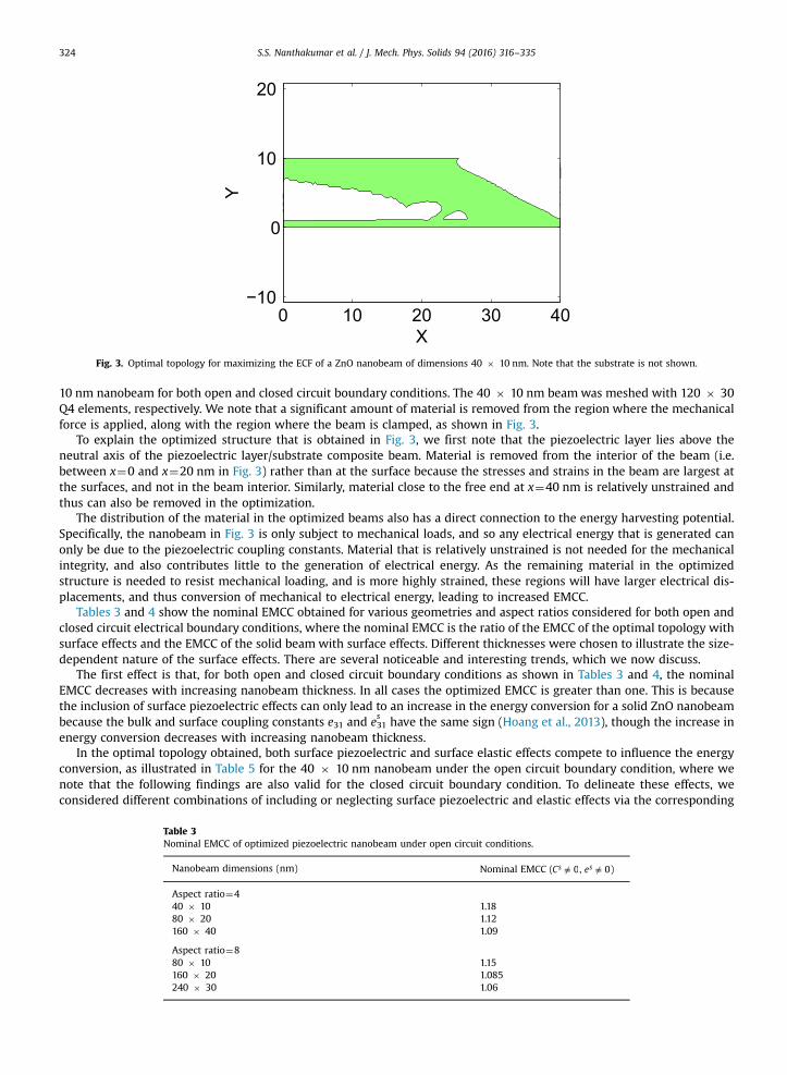
In this section we study the energy harvesting capability of a piezoelectric nanobeam, nanoplate and a cantilever energyharvester with nanoscale piezoelectric layers. We also perform topology optimization of these piezoelectric structures. Weconsider examples both with and without surface elasticity and piezoelectricity to examine the effects that surface effectshave on the energy harvesting ability. In all examples, ZnO is the piezoelectric material of choice, where the surface elasticand piezoelectric properties of ZnO are shown in Tables 1 and 2 (Hoang et al., 2013).
5.1. Two-dimensional piezoelectric nanobeam
5.1.1. Finite element model validationIn our first example, we consider a two-dimensional cantilever beam of dimension 200 � 10 nm subject to constant
mechanical load at the free end. The beam is meshed with 200 � 10 4-node bilinear quadrilateral (Q4) finite elements, andthe poling direction is vertically upwards along the thickness direction. The bulk electromechanical coupling coefficient(EMCCb) for this case can be analytically obtained by the following expression (Trinidade and Benjeddou, 2009):
Table 2Electromechanical properties of ZnO surfaces.
Elastic constants Piezoelectric constants
C11s ¼44.2 N/m e31
s ¼�0.216 nC/mC12s ¼14.2 N/m e33
s ¼0.451 nC/mC13s ¼14.2 N/m e15
s ¼�0.253 nC/mC33s ¼35 N/m
C44s ¼11.7 N/m
thickness,h (nm)0 50 100 150 200
nom
inal
EC
F
1
1.01
1.02
1.03
1.04
1.05
1.06AnalyticalXEM
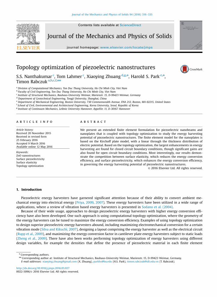
Fig. 1. Variation of nominal energy conversion factor with nanobeam thickness, with the beam aspect ratio constant at 20.
S.S. Nanthakumar et al. / J. Mech. Phys. Solids 94 (2016) 316–335 323
κ=
( + ) ( )EMCC
eC e 53
b312
11 33 312
The expression including surface effects can be obtained based on the derivation given in Yan and Jiang (2011a) for thisexample problem as
κ κ= +
( + ) + ( + ) ( )EMCC
h e e eh C e C e e
22 54
s
s
s s312
31 31
11 33 312
11 33 31 31
Fig. 1 shows the variation of ECF with increasing nanobeam depth for a constant aspect ratio of 20, where the y-axis of thefigure plots the nominal EMCC, or the value EMCC EMCC/s b. This aspect ratio is chosen as it is clear in plane strain conditionsfrom Eq. (54) that the ECF is dependent only on the nanobeam thickness. As expected the surface elastic and piezoelectriceffects lose their significance as the thickness increases. The plot shows good agreement between XFEM and the analyticalresults, validating the proposed computational formulation.
5.1.2. Optimization of two-dimensional piezoelectric nanobeamWe now perform topology optimization of the two-dimensional nanobeams under both open and closed circuit
boundary conditions to examine not only the enhancements in energy conversion that are possible, but also to delineate therelative effects of surface piezoelectricity and elasticity on the energy conversion. To do so, we again subject the cantilevernanobeam to a mechanical point load acting vertically downwards at its free end, while the nanobeam is poled along thethickness direction.
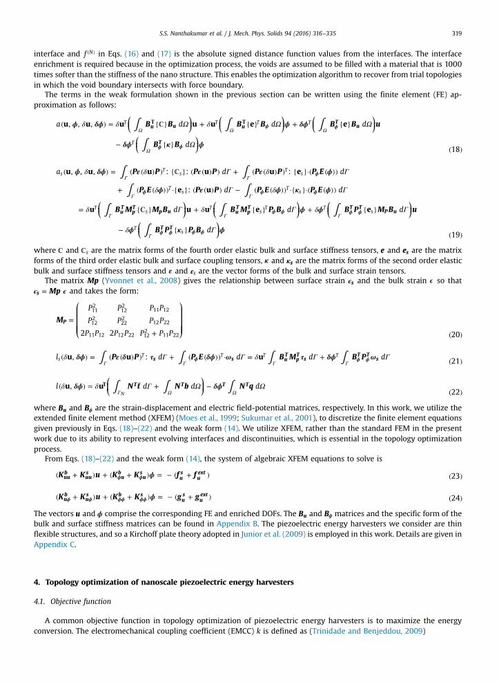
The nanobeam is placed over a substrate made of material with Young's modulus of E¼150 GPa, where the substratedimensions are the same as the nanobeam, though surface effects on the substrate are neglected. As shown in Fig. 2,electrodes are placed above and below the nanobeam. Open circuit conditions are achieved by grounding the bottomelectrode while the top electrode is free to take any potential value, while in closed circuit both the top and bottomelectrodes are grounded.
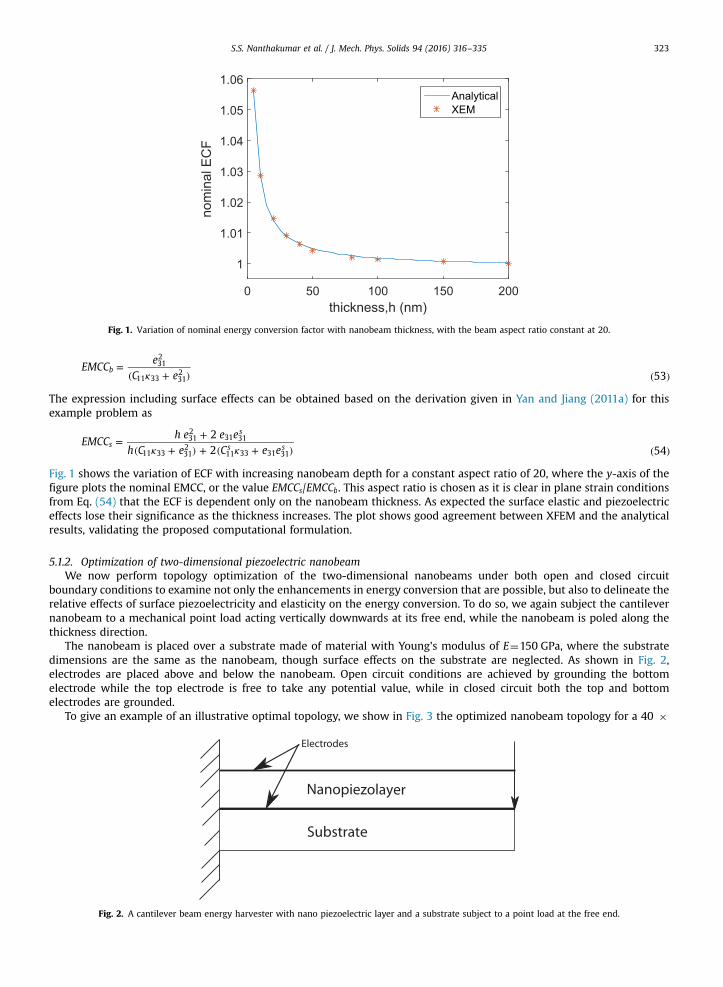
To give an example of an illustrative optimal topology, we show in Fig. 3 the optimized nanobeam topology for a 40 �
Fig. 2. A cantilever beam energy harvester with nano piezoelectric layer and a substrate subject to a point load at the free end.
X
Y
0 10 20 30 40−10
0
10
20
Fig. 3. Optimal topology for maximizing the ECF of a ZnO nanobeam of dimensions 40 � 10 nm. Note that the substrate is not shown.
S.S. Nanthakumar et al. / J. Mech. Phys. Solids 94 (2016) 316–335324
10 nm nanobeam for both open and closed circuit boundary conditions. The 40 � 10 nm beam was meshed with 120 � 30Q4 elements, respectively. We note that a significant amount of material is removed from the region where the mechanicalforce is applied, along with the region where the beam is clamped, as shown in Fig. 3.
To explain the optimized structure that is obtained in Fig. 3, we first note that the piezoelectric layer lies above theneutral axis of the piezoelectric layer/substrate composite beam. Material is removed from the interior of the beam (i.e.between x¼0 and x¼20 nm in Fig. 3) rather than at the surface because the stresses and strains in the beam are largest atthe surfaces, and not in the beam interior. Similarly, material close to the free end at x¼40 nm is relatively unstrained andthus can also be removed in the optimization.
The distribution of the material in the optimized beams also has a direct connection to the energy harvesting potential.Specifically, the nanobeam in Fig. 3 is only subject to mechanical loads, and so any electrical energy that is generated canonly be due to the piezoelectric coupling constants. Material that is relatively unstrained is not needed for the mechanicalintegrity, and also contributes little to the generation of electrical energy. As the remaining material in the optimizedstructure is needed to resist mechanical loading, and is more highly strained, these regions will have larger electrical dis-placements, and thus conversion of mechanical to electrical energy, leading to increased EMCC.
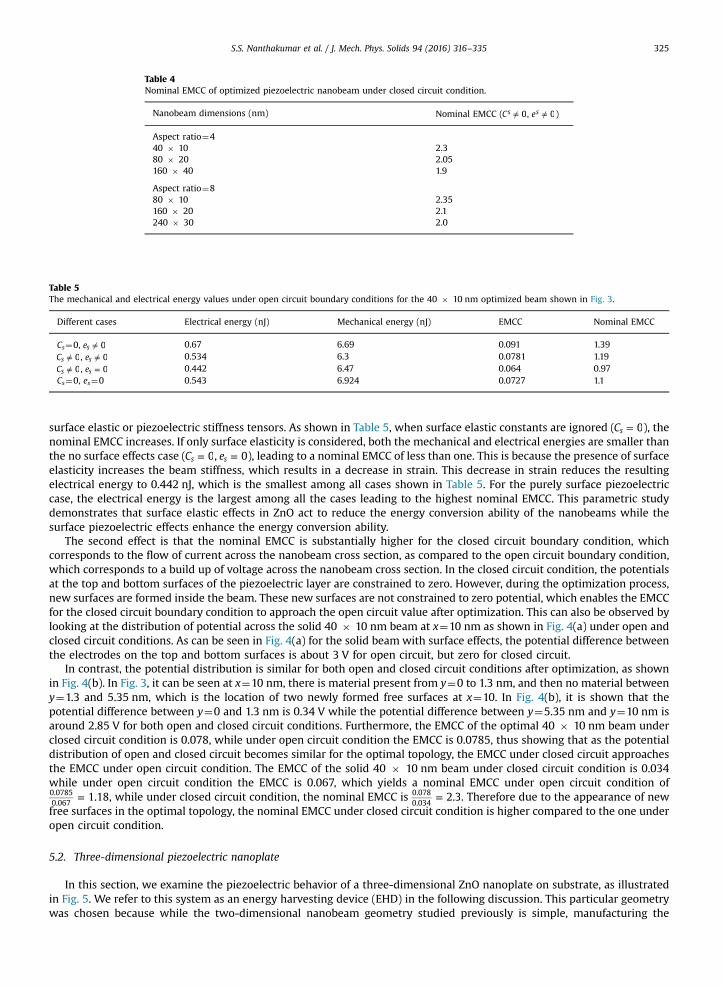
Tables 3 and 4 show the nominal EMCC obtained for various geometries and aspect ratios considered for both open andclosed circuit electrical boundary conditions, where the nominal EMCC is the ratio of the EMCC of the optimal topology withsurface effects and the EMCC of the solid beam with surface effects. Different thicknesses were chosen to illustrate the size-dependent nature of the surface effects. There are several noticeable and interesting trends, which we now discuss.
The first effect is that, for both open and closed circuit boundary conditions as shown in Tables 3 and 4, the nominalEMCC decreases with increasing nanobeam thickness. In all cases the optimized EMCC is greater than one. This is becausethe inclusion of surface piezoelectric effects can only lead to an increase in the energy conversion for a solid ZnO nanobeambecause the bulk and surface coupling constants e31 and e31
shave the same sign (Hoang et al., 2013), though the increase in
energy conversion decreases with increasing nanobeam thickness.In the optimal topology obtained, both surface piezoelectric and surface elastic effects compete to influence the energy
conversion, as illustrated in Table 5 for the 40 � 10 nm nanobeam under the open circuit boundary condition, where wenote that the following findings are also valid for the closed circuit boundary condition. To delineate these effects, weconsidered different combinations of including or neglecting surface piezoelectric and elastic effects via the corresponding
Table 3Nominal EMCC of optimized piezoelectric nanobeam under open circuit conditions.
S.S. Nanthakumar et al. / J. Mech. Phys. Solids 94 (2016) 316–335 325
surface elastic or piezoelectric stiffness tensors. As shown in Table 5, when surface elastic constants are ignored ( =C 0s ), thenominal EMCC increases. If only surface elasticity is considered, both the mechanical and electrical energies are smaller thanthe no surface effects case ( =C 0s , =e 0s ), leading to a nominal EMCC of less than one. This is because the presence of surfaceelasticity increases the beam stiffness, which results in a decrease in strain. This decrease in strain reduces the resultingelectrical energy to 0.442 nJ, which is the smallest among all cases shown in Table 5. For the purely surface piezoelectriccase, the electrical energy is the largest among all the cases leading to the highest nominal EMCC. This parametric studydemonstrates that surface elastic effects in ZnO act to reduce the energy conversion ability of the nanobeams while thesurface piezoelectric effects enhance the energy conversion ability.
The second effect is that the nominal EMCC is substantially higher for the closed circuit boundary condition, whichcorresponds to the flow of current across the nanobeam cross section, as compared to the open circuit boundary condition,which corresponds to a build up of voltage across the nanobeam cross section. In the closed circuit condition, the potentialsat the top and bottom surfaces of the piezoelectric layer are constrained to zero. However, during the optimization process,new surfaces are formed inside the beam. These new surfaces are not constrained to zero potential, which enables the EMCCfor the closed circuit boundary condition to approach the open circuit value after optimization. This can also be observed bylooking at the distribution of potential across the solid 40 � 10 nm beam at x¼10 nm as shown in Fig. 4(a) under open andclosed circuit conditions. As can be seen in Fig. 4(a) for the solid beam with surface effects, the potential difference betweenthe electrodes on the top and bottom surfaces is about 3 V for open circuit, but zero for closed circuit.
In contrast, the potential distribution is similar for both open and closed circuit conditions after optimization, as shownin Fig. 4(b). In Fig. 3, it can be seen at x¼10 nm, there is material present from y¼0 to 1.3 nm, and then no material betweeny¼1.3 and 5.35 nm, which is the location of two newly formed free surfaces at x¼10. In Fig. 4(b), it is shown that thepotential difference between y¼0 and 1.3 nm is 0.34 V while the potential difference between y¼5.35 nm and y¼10 nm isaround 2.85 V for both open and closed circuit conditions. Furthermore, the EMCC of the optimal 40 � 10 nm beam underclosed circuit condition is 0.078, while under open circuit condition the EMCC is 0.0785, thus showing that as the potentialdistribution of open and closed circuit becomes similar for the optimal topology, the EMCC under closed circuit approachesthe EMCC under open circuit condition. The EMCC of the solid 40 � 10 nm beam under closed circuit condition is 0.034while under open circuit condition the EMCC is 0.067, which yields a nominal EMCC under open circuit condition of
= 1.180.07850.067
, while under closed circuit condition, the nominal EMCC is = 2.30.0780.034
. Therefore due to the appearance of newfree surfaces in the optimal topology, the nominal EMCC under closed circuit condition is higher compared to the one underopen circuit condition.
5.2. Three-dimensional piezoelectric nanoplate
In this section, we examine the piezoelectric behavior of a three-dimensional ZnO nanoplate on substrate, as illustratedin Fig. 5. We refer to this system as an energy harvesting device (EHD) in the following discussion. This particular geometrywas chosen because while the two-dimensional nanobeam geometry studied previously is simple, manufacturing the
Fig. 4. Electrical potential distribution across the thickness of the 40 � 10 nm, (a) solid beam and (b) optimal beam from Fig. 3, at x¼10 nm.
Fig. 5. A piezoelectric ZnO nanoplate on substrate subjected to point load, F at free end, with P indicating the poling direction.
S.S. Nanthakumar et al. / J. Mech. Phys. Solids 94 (2016) 316–335326
20 40 60 80 100 120 14074
76
78
80
82
84
86
88
AnalyticalXFEM
Fig. 6. Variation of dimensionless maximum deflection with depth of plate.
S.S. Nanthakumar et al. / J. Mech. Phys. Solids 94 (2016) 316–335 327
complex shapes that emerge from the topology optimization may pose significant challenges, particularly with a beamthickness of around 10 nm. In this example, the thickness of the nano plate is fixed while the in-plane topology of the nanoplate is altered. Thus, the holes that are formed through the thickness, which have feature sizes larger than tens of nan-ometers, could likely be lithographically manufactured using technology that is available today.
5.2.1. Finite element model validationAn analytic expression for the deflection of a piezoelectric nanoplate including surface piezoelectric and elastic effects
based on Kirchoff plate theory was recently given by Wang (2012) as
∑ ∑ π π( ) =( )=
∞
=
∞ ⎛⎝⎜⎜
⎞⎠⎟⎟
⎛⎝⎜⎜
⎞⎠⎟⎟w x y A
m xa
n yb
, sin sin55m n
mn1 1
where
π= ( )A
qmn Y
1656mn 2
κ κπ π
κ κπ
= + + + +
+ + + + +( )
∼ ∼
∼ ∼
∼
∼
∼ ∼
∼ ∼
⎜ ⎟ ⎜ ⎟⎡⎣⎢⎢
⎛⎝⎜⎜
⎞⎠⎟⎟
⎛⎝⎜⎜
⎞⎠⎟⎟
⎤⎦⎥⎥
⎡⎣⎢⎢
⎛⎝
⎞⎠
⎛⎝
⎞⎠
⎤⎦⎥⎥
⎡⎣⎢⎢
⎛⎝⎜⎜
⎞⎠⎟⎟
⎛⎝⎜⎜
⎞⎠⎟⎟
⎤⎦⎥⎥
⎛⎝⎜⎜
⎞⎠⎟⎟
Y ce h
ce e h
Xma
nb
ce h
c ce e
h Xm n
a b
12 2
62
57
ss
s ss
11312
33
3
1131 31
33
2 4 4
12312
33
3
66 1231 31
33
22 2 4
2 2
q refers to uniformly distributed load over the plate; = −∼c cc
c11 11132
33, = −∼c c
c
c12 12132
33, = −∼e e c e
c31 3113 33
33. κ κ= −∼ e
c33 33332
33and m,
n¼1,3,5 …The FE model of the piezoelectric nano plate is performed by an equivalent 2D model as discussed in Appendix C.The approximation of the electric potential field is made by discretizing the plate into several sublayers with linear
variation of electric potential within each sublayer (Wang, 2004). The number of sublayers for electric potential dis-cretizaton is taken to be 10. The piezoelectric plate considered in this example is poled vertically along the z-direction asshown in Fig. 5. Fig. 6 shows good agreement between the analytic and FE solutions, where the dimensions of the nano platewere 200 � 50 nm for the length and width, while the depth was varied from 10 to 100 nm.
5.2.2. Optimization of piezoelectric nanoplate layerThe EHD is composed of a substrate and a piezoelectric ZnO nanoplate, as shown in Fig. 5. The substrate is assumed to be
made of aluminum, and the thickness of the substrate, Hs and the piezoelectric layer, Hp are taken to be 125 nm and 100 nmrespectively. The length and width of this EHD is assumed to be × μ4 2 m. Two electrical boundary conditions are
X0 500 1000 1500 2000 2500 3000 3500 4000
Y0
500
1000
1500
2000
X0 500 1000 1500 2000 2500 3000 3500 4000
Y
0
500
1000
1500
2000
Fig. 7. Optimized topology (top view) of the piezoelectric layer (top view) of an EHD subjected to point load at free end. (a) 100 nm thick nanoplate;(b) 10 nm thick nanoplate. Same optimized topology obtained for both open and closed circuit boundary conditions.
thickness of piezo layer (nm)0 50 100 150
perc
enta
ge in
crea
se in
EM
CC
10%
20%
30%
40%
50%
60%
70%
80%Cs 0, es 0Cs = 0, es 0Cs 0, es = 0
Fig. 8. The percentage increase in EMCC with varying thickness of the piezoelectric nanoplate under closed circuit boundary conditions.
S.S. Nanthakumar et al. / J. Mech. Phys. Solids 94 (2016) 316–335328
considered, with electrodes on the top of the nanoplate and underneath the substrate. In closed circuit boundary condition,both the top and bottom electrodes are grounded. In open circuit boundary condition, only the bottom electrode isgrounded.
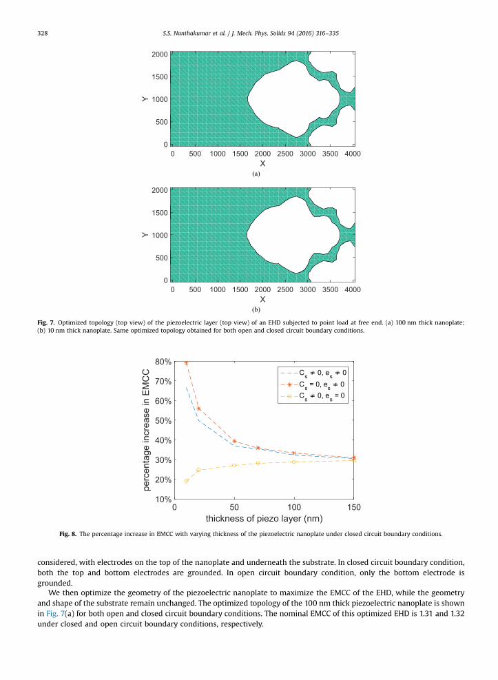
We then optimize the geometry of the piezoelectric nanoplate to maximize the EMCC of the EHD, while the geometryand shape of the substrate remain unchanged. The optimized topology of the 100 nm thick piezoelectric nanoplate is shownin Fig. 7(a) for both open and closed circuit boundary conditions. The nominal EMCC of this optimized EHD is 1.31 and 1.32under closed and open circuit boundary conditions, respectively.
Table 6Comparison of nominal EMCC between solid and optimized piezoelectric nanoplate of dimension 4000 � 2000 � 10 nm under open circuit condition inan EHD.
Fig. 9. Top view of (a) solid nanoplate and (b) a random optimal topology under open circuit boundary conditions. The thickness of the nanoplate is 10 nm.
S.S. Nanthakumar et al. / J. Mech. Phys. Solids 94 (2016) 316–335 329
To examine size effects on the EMCC and optimized topology, we studied the effect of replacing the 100 nm nanoplatewith a 10 nm thick nanoplate, with the optimized topology for the 10 nm nanoplate shown in Fig. 7(b). The optimumtopologies are similar to those seen previously for the two-dimensional nanobeam, in that some material around the pointforce is removed, along with a section of the nanobeam away from the loading surface. The nominal EMCC of the optimizedEHD for 10 nm thick piezoelectric layer is 1.29 and 1.28 under closed and open circuit conditions respectively. The optimizedtopology and the nominal EMCC for the 100 nm and 10 nm piezoelectric layers remain similar. This shows that, at least forthe nanoplate geometry, the presence of surface effects does not influence the optimum topology for the maximum energyconversion objective function.
X
Y
0 1000 2000 3000 4000−500
0
500
1000
1500
2000
2500
Fig. 10. Top view of the optimal topology for the maximum energy conversion objective function with a constraint on the increase in EMCC. The thicknessof the nanoplate is 10 nm.
S.S. Nanthakumar et al. / J. Mech. Phys. Solids 94 (2016) 316–335330
While the optimal topology may not change substantially, surface effects and optimization combine to significantlyincrease the energy harvesting capability of piezoelectric nanoplates. For example, the ratio of the EMCC of a 100 nm thicknanoplate with surface effects to the EMCC of a 100 nm nanoplate ignoring surface effects is 1.03 and 1.01 under closed andopen circuit conditions respectively. However, the EMCC after optimization is 0.0163 and 0.059 under closed and opencircuit conditions, resulting in an increase of 32% and 29% under closed and open circuit boundary conditions respectively.Furthermore, the ratio of the EMCC of a 10 nm thick nanoplate with surface effects to the EMCC of a 10 nm thick nanoplateignoring surface effects is 1.39 and 1.18 under closed and open circuit conditions respectively. However, with optimizationand surface effects, the EMCC is 0.021 and 0.067 for closed and open circuit conditions, leading to a combined increase inEMCC due to optimization and surface effects of 68% and 46%, respectively.
Fig. 8 shows the change in the EMCC as a function of the thickness of the piezoelectric nanoplate under closed circuitconditions. Similar, but slightly smaller increases are seen for open circuit conditions. The figure shows the interactionbetween surface elastic and surface piezoelectric effects in controlling the energy conversion of the EHD. With decrease inthickness of the nanoplate, the surface elastic effects increase the stiffness of the plate and thus the mechanical energy,leading to reduction in energy conversion. In contrast, the surface piezoelectric effects enhance the coupling abilityleading to an increase in energy conversion of the EHD overcoming the reduction caused by the surface elastic effects. Itcan also be seen from the figure that for the case =C 0s ; ≠e 0s the energy conversion is a maximum. This is because underthis case, there is only an increase in piezoelectric coupling and no increase in stiffness of the plate with decreasingthickness.
Table 6 shows the mechanical energy, electrical energy and EMCC for a solid piezoelectric nanoplate from Fig. 9(a), arandom optimal topology in Fig. 9(b), and the calculated optimal topology from Fig. 7(b) under open circuit conditions. Asshown in Table 6, though there is a slight increase in mechanical strain energy from reducing the volume fraction, there is asignificant increase in electrical energy as material gets distributed to the optimal topology shown in Fig. 7(b). From Table 6,it is also clear that for the same volume fraction as the optimum topology, random removal of material like the one shown inFig. 9(b) results in a considerable increase in mechanical strain energy with only a modest increase in electrical energy,leading to a reduction in the EMCC.
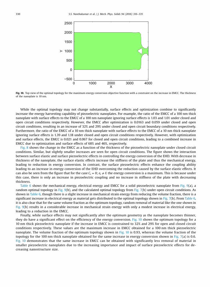
Finally, while surface effects may not significantly alter the optimum geometry as the nanoplate becomes thinner,they do have a significant effect on the efficiency of the energy conversion. Fig. 10 shows the optimum topology for a10 nm thick piezoelectric nanoplate if the increase in EMCC is constrained to 32% and 29% for open and closed circuitconditions respectively. These values are the maximum increase in EMCC obtained for a 100 nm thick piezoelectricnanoplate. The volume fraction of the optimum topology shown in Fig. 10 is 0.93, whereas the volume fraction of thetopology for the 100 nm thick nanoplate obtained for the same increase in energy conversion shown in Fig. 7(a) is 0.6.Fig. 10 demonstrates that the same increase in EMCC can be obtained with significantly less removal of material insmaller piezoelectric nanoplates due to the increasing importance and impact of surface piezoelectric effects for de-creasing nanostructure size.
S.S. Nanthakumar et al. / J. Mech. Phys. Solids 94 (2016) 316–335 331
6. Conclusion
In conclusion, we have formulated and presented a new extended finite element model that is coupled to topologyoptimization to study the energy harvesting potential of piezoelectric nanostructures. Our simulations have demonstratedthe improvements in energy conversion efficiency that can be realized due to a combination of surface effects and topologyoptimization. We have also elucidated the competition between surface elastic and surface piezoelectric effects in con-trolling the overall energy conversion efficiency of the piezoelectric nanostructures.
Appendix A. Derivation of adjoint problem
The objective function and its constraints are as follows:Minimize
Ψ ΠΠ
( ) = =( )
Jk
Minimize1
A.1e
d2
∫ Ω − ¯ = ( )Ωd VSubject to 0 A.2
ϕ δϕ ϕ δϕ δϕ δϕδ δ δ δ( ) + ( ) = − ( ) + ( ) ( )a a l lu u u u u u, , , , , , , , A.3s s
ϕ ψ ϕ ψ= + ( ) − ( ) − ( ) − ( ) ( )L J l a a lw u w u w w, , , , , , . A.8s s
The material derivative of the Lagrangian is defined as
ϕ ψ ϕ ψ = + ( ) − ( ) − ( ) − ( ) ( )L J l a a lw u w u w w, , , , , , . A.9s s
All the terms that contain ′u and ϕ′ in the material derivative of Lagrangian are collected and the sum of these terms is setto zero, to get the weak form of the adjoint equation,
S.S. Nanthakumar et al. / J. Mech. Phys. Solids 94 (2016) 316–335332
∫ ∫ ∫∫ ∫
ϵ ϵ ϵ ψ ϵ ϵ
ϵ ψ ϵ ϵ
Ω Ω Γ
Γ Ω
( ′) ( ) − ( ′) · ( ) − ( ′) ( )
− ( ′) · ( ) = ( ′) ( ) ( )
Ω Ω Γ
Γ Ω
u e E C w
u e E u u
d d d
d C d
u w u: : : : :
: 2 : : A.10
s s s
s s s
T bulk T T T
T T T bulk1
∫ ∫ ∫∫ ∫
ϕ ϵ ϕ κ ψ ϕ ϵ
ϕ κ ψ ϕ κ ϕ
Ω Ω Γ
Γ Ω
( ′) · ( ) − ( ′) · · ( ) − ( ′) · ( )
− ( ′) · · = ( ′) · · ( ) ( )
Ω Ω Γ
Γ Ω
E e w E E E e w
E E E E
d d d
d C d
: :
2 A.11
s s s
s s s
T bulk T T
T T2
Appendix B. Bulk and surface stiffness matrices
The bulk and surface stiffness matrices corresponding to the discrete finite element equations in Eq. (24) are defined asfollows:
∫∫
Ω
Γ
= { }
= { } ( )
Ω
Γ
K B B
K B M M B
d
d B.1
uub
uT
u
uus
uT
pT
p us
∫∫
Ω
Γ
= { }
= { } ( )
ϕ ϕ
ϕ ϕ ϕ
Ω
Γ
K B B
K B P M B
d
d
e
e B.2
ub
u
us T
p u
T
Ts
∫∫
Ω
Γ
= { }
= { } ( )
ϕ ϕ
ϕ ϕ ϕ
Ω
Γ
K B B
K B M P B
d
d
e
e B.3
ub
u
us
u PT
T T
T Ts
∫∫
κ
κ
Ω
Γ
= − { }
= − { } ( )
ϕϕ ϕ ϕ
ϕϕ ϕ ϕ
Ω
Γ
K B B
K B P PB
d
d B.4
b
s Ts
T
T
∫∫ ∫
∫∫
τ
ω
Γ
Γ Ω
Γ
Ω
=
= ¯ +
=
= − ( )
ϕ
Γ
Γ Ω
Γ
Ω
f B M
f N t N b
g B P
g N q
d
d d
d
d B.5
us
uT
pT
s
uext T T
us T T
s
uext T
N
Here P is the tangential projection tensor to Γ at Γ∈x which is defined as ( ) = − ( ) ⊗ ( )P x I n x n x , I is the second order unittensor. Mp is defined as
=
+ ( )
⎛
⎝
⎜⎜⎜⎜
⎞
⎠
⎟⎟⎟⎟M
P P P P
P P P P
P P P P P P P2 2 B.6
P
112
122
11 12
122
222
12 22
11 12 12 22 122
11 22
The matrices Bu and ϕB comprise standard FEM and enrichment parts. The Bu and ϕB matrices are
S.S. Nanthakumar et al. / J. Mech. Phys. Solids 94 (2016) 316–335 333
=
=
=+
++ +
=
=
=++
( )
ϕ ϕ ϕ
ϕ
ϕ
⎡
⎣
⎢⎢⎢
⎤
⎦
⎥⎥⎥
⎛
⎝
⎜⎜⎜
⎞
⎠
⎟⎟⎟⎛
⎝
⎜⎜⎜
⎞
⎠
⎟⎟⎟⎡
⎣
⎢⎢⎢
⎤
⎦
⎥⎥⎥
⎛
⎝
⎜⎜⎜
⎞
⎠
⎟⎟⎟⎛
⎝
⎜⎜⎜
⎞
⎠
⎟⎟⎟
B B B
B
B
B B B
B
B
NN
N N
f N f x N
f N f y N
f N f y N f N f x N
NN
f N f x N
f N f y N
00
, 0
0 ,
, ,
,
,B.7
u u std u enr
u std
u enr
std enr
std
enr
x
y
y x
x
y
y x
x
y
x
y
, ,
,
,
, ,
,
,
The enrichment f used for modelling weak discontinuity is (Moes et al., 2003)
∑ ∑Ψ Ψ= | | −( )∈ ∈
f N NB.8i I
i ii I
i i
Appendix C. Finite element model of a piezoelectric nanoplate
Piezoelectric energy harvesters are usually thin flexible structures and so Kirchoff plate theory adopted in Junior et al.(2009) is employed in this work. A rectangular finite element with three mechanical degrees of freedom (u, v and w in x, yand z directions) is adopted to model displacements in substructure and nano-piezo layer. The transverse displacement isassumed to vary in polynomial form in an element,
( ) = ( )Taw x C.1
where the polynomial terms
= [ ] ( )T x y x xy y x x y xy y x y xy1 C.22 2 3 2 2 3 3 3
a is a vector of generalized coordinates. w(x) in terms of nodal displacements can written as
= ( )NWw C.3
where = −N TA 1, A is a 12 � 12 transformation matrix comprising nodal values of T and its derivatives whileW is a vector ofnodal variables. The vector of curvatures can be expressed as follows:
Fig. C1. Discretization for electric potential field with top and bottom layers having surface material properties.
S.S. Nanthakumar et al. / J. Mech. Phys. Solids 94 (2016) 316–335334
∂∂
∂∂
∂∂ ∂
=( )
⎡⎣⎢
⎤⎦⎥ B W
wx
wy
wx y
2C.4
u
T2
2
2
2
2
Approximation of electric potential field can be obtained by discretizing the nano-piezoelectric plate into sublayers asshown in Fig. C1 with linear potential distribution across the thickness for each sublayer as presented in Wang (2004).
The electric potential field across the thickness can be defined as
ϕϕ ( ) = ¯ ( )ϕz N C.5kk k
where ϕNk is the shape function of the electric potential function and ϕk denotes electric potential at top and bottom surfacesof the sublayer
= [ − − ]( )ϕ +
tz z z zN
1C.6
k
ii i 1
where ti is the thickness of the sublayer. The electric field for each sublayer element is
ϕ= ¯ ( )ϕE B C.7kk k
where = [ − ]ϕB 1 1kt1
iand ϕ ϕ ϕ¯ = [ ]+k k k T1 .
The element stiffness matrix as given in Junior et al. (2009) is
∫ ∫∫ ∫ κ
Ψ Ω Ψ Ω
Ψ Ω Ψ Ω=
¯ ( ( )) ¯ ( ( ))
¯ ( ( )) ¯ ( ( ))( )
ϕ
ϕ ϕ ϕ
Ω Ω
Ω Ω
⎛
⎝
⎜⎜⎜
⎞
⎠
⎟⎟⎟KB CB B e B
B eB B B
z g x d z g x d
z g x d g x dC.8
u u u
u
T T T
T T
2
C , e and κ are the plane stress (2D) constants in terms of 3D material constants (Junior et al., 2009). The “ersatz material”approach is adopted to model the voids. The stiffness matrix is obtained by numerically integrating over subtriangles oneither sides of the inclusion interface. Replacing voids by a weak material, helps the optimization algorithm to recover fromtrial topologies in which the void boundary intersects with force boundary.
Note that enrichment functions are not used and so there is no change in the degrees of freedom with iterations in theoptimization process. As suggested in Li et al. (2012) Ψ( ( ))g x is taken as
ΨΨΨ
( ( )) =( ) ≥
− ( ) < ( )
⎧⎨⎩g xx
e x
1 01 4 0 C.9
The piezoelectric nano plate (PNP) exhibits different surface elastic and surface piezoelectric behavior compared to thebulk. The PNP may be assumed to be a bulk plate with surface elastic constants and surface piezoelectric constants at the topand bottom sublayers of the discretization for electric potential field.
The surface stiffness matrix may be defined as
∫ ∫∫ ∫ κ κ
Ω Ω
Ω Ω=
( ¯ + ¯ ) ( ¯ + ¯ )
( ¯ + ¯ ) ( ¯ + ¯ )( )
ϕ
ϕ ϕ ϕ
Ω Ω
Ω Ω
⎛
⎝
⎜⎜⎜⎜
⎞
⎠
⎟⎟⎟⎟K
B C C B B e e B
B e e B B B
z d z d
z d dC.10
s
u s u u s
s u s
Ts
T T Ts
Ts
Ts
2
s s
s s
whereΩs corresponds to the top and bottom sublayers, z is the distance of the mid-surface of the top/bottom sublayers fromthe neutral surface. Cs, es and κs are the surface elastic, piezoelectric and dielectric constants:
∫∫∫∫∫∫
κ
κ
Ω
Ω
Ω
Ω
Ω
Ω
= ( ¯ )
= ( ¯ )
= ( ¯ ) =
= ( ¯ ) =
= (¯)
= (¯ )( )
ϕ ϕ ϕ
ϕ ϕ ϕ
ϕϕ ϕ ϕ
ϕϕ ϕ ϕ
Ω
Ω
Ω
Ω
Ω
Ω
K B C B
K B C B
K B e B K
K B e B K
K B B
K B B
z d
z d
z d
z d
d
dC.11
uub
u u
uus
u s u
ub
u ub
us
u s us
b
ss
Ts
Ts
T Ts
T
T Ts
T
Ts
Ts
2
2
s
s
s
s
s
s
S.S. Nanthakumar et al. / J. Mech. Phys. Solids 94 (2016) 316–335 335
References
Agrawal, R., Espinosa, H.D., 2011. Giant piezoelectric size effects in zinc oxide and gallium nitride nanowires. A first principles investigation. Nano Lett. 11,786–790.
Allaire, G., Jouve, F., Toader, A.M., 2004. Structural optimization using sensitivity analysis and a level-set method. J. Comput. Phys. 194, 363–393.Chen, C.Q., Shi, Y., Zhang, Y.S., Zhu, J., Yan, Y.J., 2006. Size dependence of Young's modulus in zno nanowires. Phys. Rev. Lett. 96, 075505.Chen, S., Gonella, S., Chen, W., Liu, W.K., 2010. A level set approach for optimal design of smart energy harvesters. Comput. Methods Appl. Mech. Eng. 199,
2532–2543.Choi, K.K., Kim, N.H., 2005. Structural Sensitivity Analysis and Optimization. Springer, New York.Dai, S., Park, H.S., 2013. Surface effects on the piezoelectricity of zno nanowires. J. Phys. Mech. Solids 61.Dai, S., Gharbi, M., Sharma, P., Park, H.S., 2011. Surface piezoelectricity: size-effects in nanostructures and the emergence of piezoelectricity in non-
piezoelectric materials. J. Appl. Phys. 110, 104305.Espinosa, H.D., Bernal, R.A., Minary-Jolandan, M., 2012. A review of mechanical and electromechanical properties of piezoelectric nanowires. Adv. Mater. 24,
4656–4675.Farsad, M., Vernerey, F.J., Park, H.S., 2010. An extended finite element/level set method to study surface effects on the mechanical behavior and properties of
nanomaterials. Int. J. Numer. Methods Eng. 84, 1466–1489.Gurtin, M.E., Murdoch, A.I., 1975. A continuum theory of elastic material surfaces. Arch. Ration. Mech. Anal. 57, 291–323.Gurtin, M.E., Weissmller, J., Larché, F., 1998. A general theory of curved deformable interfaces in solids at equilibrium. Philos. Mag. 75, 1093–1109.Hoang, M.-T., Yvonnet, J., Mitrushchenkov, A., Chambaud, G., 2013. First-principles based multiscale model of piezoelectric nanowires with surface effects. J.
Appl. Phys. 113.Junior, C.D.M., Erturk, A., Inman, D.J., 2009. An electromechanical finite element model for piezoelectric energy harvester plates. J. Sound Vib. 327, 9–25.Li, L., Wang, M.Y., Wei, P., 2012. XFEM schemes for level set based structural optimization. Front. Mech. Eng. 7 (4), 335–356.Mitrushchenkov, A., Linguerri, R., Chambaud, G., 2009. Piezoelectric properties of AlN, ZnO, and HgxZn1�xO nanowires by first-principles calculations. J.
Phys. Chem. C 113.Moes, N., Dolbow, J., Belytschko, T., 1999. A finite element method for crack growth without remeshing. Int. J. Numer. Methods Eng. 46, 133–150.Moes, N., Cloirec, M., Cartraud, P., Remacle, J.F., 2003. A computational approach to handle complex microstructure geometries. Comput. Methods Appl.
Mech. Eng. 192, 3163–3177.Momeni, K., Odegard, G.M., Yassar, R.S., 2012a. Finite size effect on the piezoelectric properties of zno nanobelts: a molecular dynamics approach. Acta
Mater. 60.Momeni, K., Odegard, G.M., Yassar, R.S., 2012b. Finite size effect on the piezoelectric properties of zno nanobelts: a molecular dynamics approach. Acta
Mater. 60, 5117–5124.Nakasone, P., Silva, E., 2009. Design of piezoelectric energy harvesting devices and laminate structures by applying topology optimization, modeling, signal
processing, and control for smart structures. Proc. SPIE 728601–728611.Nanthakumar, S.S., Lahmer, T., Rabczuk, T., 2013. Detection of flaws in piezoelectric structures using extended FEM. Int. J. Numer. Methods Eng. 96, 373–389.Nanthakumar, S.S., Lahmer, T., Rabczuk, T., 2014. Detection of multiple flaws in piezoelectric structures using XFEM and level sets. Comput. Methods Appl.
Mech. Eng. 275, 98–112.Nanthakumar, S.S., Lahmer, T., Zhuang, X., Zi, G., Rabczuk, T., 2016. Detection of material interfaces using a regularized level set method in piezoelectric
structures. Inverse Probl. Sci. Eng 24 (1), 153–176, http://dx.doi.org/10.1080/17415977.2015.1017485.Osher, S.J., Sethian, J.A., 1988. Fronts propagating with curvature dependent speed: algorithms based on the Hamilton–Jacobi formulation. J. Comput. Phys.
79, 12–49.Priya, S., 2007. Advances in energy harvesting using low profile piezoelectric transducers. J. Electroceram. 19, 167–184.Priya, D.I.S., 2009. Energy Harvesting Technologies. Springer, US, http://dx.doi.org/10.1007/978-0-387-76464-1.Rupp, C.J., Evgrafov, A., Maute, k., Dunn, M.L., 2009. Design of piezoelectric energy harvesting systems: a topology optimization approach based on
multilayer plates and shells. J. Intell. Mater. Syst. Struct. 16, 1923–1939.Silva, E.C.N., Kikuchi, N., 2007. Design of piezoelectric transducers using topology optimization. J. Electroceram. 19, 167–184.Sodano, H.A., Inman, D.J., Park, G., 2004. A review of power harvesting from vibration using piezoelectric materials. Shock Vib. Dig. 36, 197–205.Sukumar, N., Chopp, D.L., Moes, N., Belytschko, T., 2001. Modeling holes and inclusions by level sets in the extended finite-element method. Comput.
Methods Appl. Mech. Eng. 190, 6183–6200.Trinidade, M.A., Benjeddou, A., 2009. Effective electromechanical coupling coefficients of piezoelectric adaptive structures: critical evaluation and opti-
mization. Mech. Adv. Mater. Struct. 16, 210–223.Wang, S.Y., 2004. A finite element model for the static and dynamic analysis of a piezoelectric bimorph. Int. J. Solids Struct. 41, 4075–4096.Wang, S.Y., 2012. Surface effects on the electroelastic responses of a thin piezoelectric plate with nanoscale thickness. J. Phys. D: Appl. Phys. 45, 255401.Wang, Z.L., Song, J., 2006. Piezoelectric nanogenerators based on zinc oxide nanowire arrays. Science 312, 242–246.Wang, M.Y., Wang, S.Y., 2006. Radial basis functions and level set method for structural topology optimization. Int. J. Numer. Methods Eng. 65, 2060–2090.Wang, S.Y., Lim, K.M., Khoo, B.C., Wang, M.Y., 2007. An extended level set method for shape and topology optimization. J. Comput. Phys. 221, 395–421.Wein, F., Kaltenbacher, M., Stingl, M., 2013. Topology optimization of a cantilevered piezoelectric energy harvester using stress norm constraints. Struct.
Multidiscip. Optim. 48, 173–185.Wendland, H., 1995. Piecewise polynomial, positive definite and compactly supported radial functions of minimal degree. Adv. Comput. Math. 4.1, 389–396.Xu, S., Qin, Y., Xu, C., Wei, Y., Yang, R., Wang, Z.L., 2010. Self-powered nanowire devices. Nat. Nanotechnol. 5, 366–373.Yan, Z., Jiang, L., 2011a. Surface effects on the electromechanical coupling and bending behaviours of piezoelectric nanowires. J. Phys. D: Appl. Phys. 44,
075404.Yan, Z., Jiang, L.Y., 2011b. The vibrational and buckling behaviors of piezoelectric nanobeams with surface effects. Nanotechnology 22, 245703.Yvonnet, J., Quang, H.L., He, Q.C., 2008. An xfem/level set approach to modelling surface/interface effects and to computing the size-dependent effective
properties of nanocomposites. Comput. Mech. 42, 119–131.Zhao, M.H., Wang, Z.L., Mao, S.X., 2004. Piezoelectric characterization of individual zinc oxide nanobelt probed by piezoresponse force microscope. Na-
noletters 4, 587–590.Zheng, B., Chang, C., Gea, H., 2009. Topology optimization of energy harvesting devices using piezoelectric materials. Struct. Multidiscip. Optim. 38 (1), 17–23.