36
Torchmate CNC Cutting Systems Model 501A Signal Generator Hardware Guide Torchmate CNC Cutting systems Updated 3/25/08
| Date post: | 15-Mar-2018 |
| Category: |
Documents |
| Upload: | truongkhanh |
| View: | 217 times |
| Download: | 2 times |

Torchmate CNC Cutting Systems
Model 501A
Signal Generator Hardware Guide
Torchmate CNC Cutting systems
Updated 3/25/08

Table of Contents 1. GETTING STARTED ...................................................................................................................................... 1
ABOUT THIS MANUAL ................................................................................................................................................ 1 TURNING OFF THE CONTROLLER ................................................................................................................................ 1 SAFETY AND USAGE GUIDELINES ............................................................................................................................... 2
2. HARDWARE GUIDE ....................................................................................................................................... 3 OVERVIEW OF THE SIGNAL GENERATOR .................................................................................................................... 3 FRONT PANEL............................................................................................................................................................. 3 REAR PANEL .............................................................................................................................................................. 4 REMOVING THE SIGNAL GENERATOR TOP COVER ..................................................................................................... 8 JUMPER SETTINGS ...................................................................................................................................................... 8
JP83 – Chassis Ground ........................................................................................................................................ 8 JP84/JP85 – Input Power Select ........................................................................................................................... 9
INTERNAL CONNECTORS .......................................................................................................................................... 10 JP30 – Auxiliary Inputs ..................................................................................................................................... 11 JP32 – Bus Expansion ........................................................................................................................................ 12 JP33 – Step & Direction .................................................................................................................................... 12 JP40 – Input Aux Header ................................................................................................................................... 13 JP50 – Output Aux Header ................................................................................................................................ 13 JP80 – Rear Panel Power ................................................................................................................................... 14 JP81 – Rear Panel Fuse ...................................................................................................................................... 14 JP82 – Front Panel Switch ................................................................................................................................. 14
PLUG-IN CARD INTERFACES ..................................................................................................................................... 14 3. SAMPLE WIRING DIAGRAMS ................................................................................................................... 17
TYPICAL MOTOR SIGNAL CIRCUIT FOR HALF-STEPPING AND MICRO-STEPPING DRIVES ........................................ 18 TYPICAL MOTOR SIGNAL CIRCUIT II ........................................................................................................................ 19 TYPICAL MOTOR SIGNAL CIRCUIT FOR GECKO DRIVES ........................................................................................... 20 TYPICAL OUTPUT LINE CIRCUIT............................................................................................................................... 21 TYPICAL INPUT LINE CIRCUIT – INTERNAL POWER .................................................................................................. 22 TYPICAL INPUT LINE CIRCUIT – EXTERNAL POWER ................................................................................................. 23
4. APPENDIX ......................................................................................................................................................... 25 SIGNAL GENERATOR BOARD LAYOUT ..................................................................................................................... 25 CONNECTOR PIN-OUT TABLE ................................................................................................................................... 25 POWER ..................................................................................................................................................................... 28 OUTPUTS .................................................................................................................................................................. 29 INPUTS ..................................................................................................................................................................... 30 CONNECTORS ........................................................................................................................................................... 31 PLUG-IN CARD INTERFACE ...................................................................................................................................... 32

Torchmate Section 1. Getting Started
1
1. Getting Started
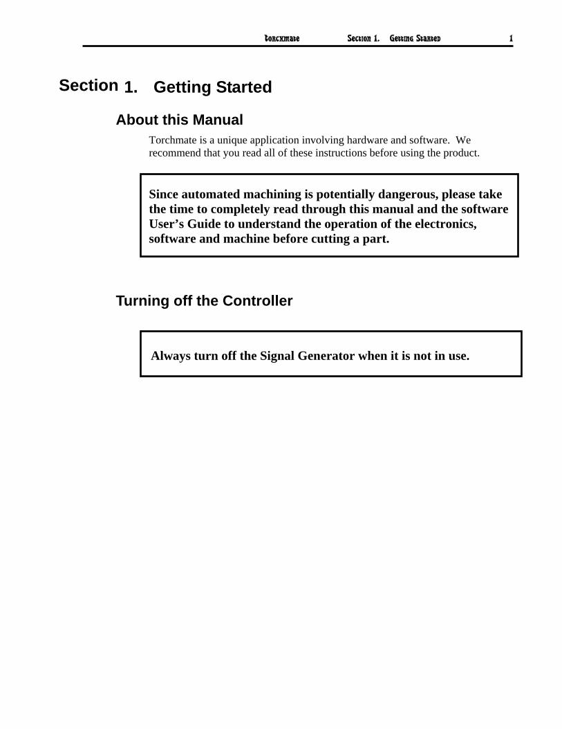
About this Manual Torchmate is a unique application involving hardware and software. We recommend that you read all of these instructions before using the product.
Since automated machining is potentially dangerous, please take the time to completely read through this manual and the software User’s Guide to understand the operation of the electronics, software and machine before cutting a part.
Turning off the Controller
Section
Always turn off the Signal Generator when it is not in use.

Torchmate Section 1. Getting Started
2
Safety and Usage Guidelines
When running an automated machine tool, safety is of the utmost importance. For proper and safe use of the Torchmate program and your CNC machine, the following safety guidelines must be followed:
1. Never let the machine tool run unattended.
2. Require any person in the same room as a running machine tool to wear safety goggles, and to stay a safe distance from the machine.
3. Allow only trained operators to run the machine tool. Any operator must have:
Knowledge of machine tool operation.
Knowledge of personal computer operation.
Knowledge of Microsoft Windows.
Good common sense.
4. Place safety guards around the machine to prevent injury from flying objects. It is highly recommended that you build a safety shield around the entire tool envelope.
5. Never place any part of your body within the tool envelope while the machine is online, since unexpected machine movement can occur at any time.
6. Always keep the tool envelope tidy and free of any loose objects.
7. Be on alert for computer crashes at all times.
Torchmate, Inc. is not responsible for the safe installation and use of this product. You and only you are responsible for the safety of yourself and others during the operation of your CNC machine tool. Torchmate supplies this product but has no control over how it is installed or used. Always be careful!
Torchmate, Inc. or its affiliates are not responsible for damage to any equipment or workpiece resulting from use of this product.
If you do not understand and agree with all of the above safety guidelines, do not use this product.
Torchmate Section 2. Hardware Guide
3
2. Hardware Guide
Overview of the Signal Generator The Signal Generator provides a flexible interface that controls up to 5 stepper or digital servo motor drivers, 8 output lines and 8 input lines. It works in conjunction with the Torchmate software. Please note that there are several software and hardware settings that affect the use of the Signal Generator. These settings are described in this manual and in the software User’s Guide. An optional I/O expansion board provides an additional 24 output and 24 input lines.
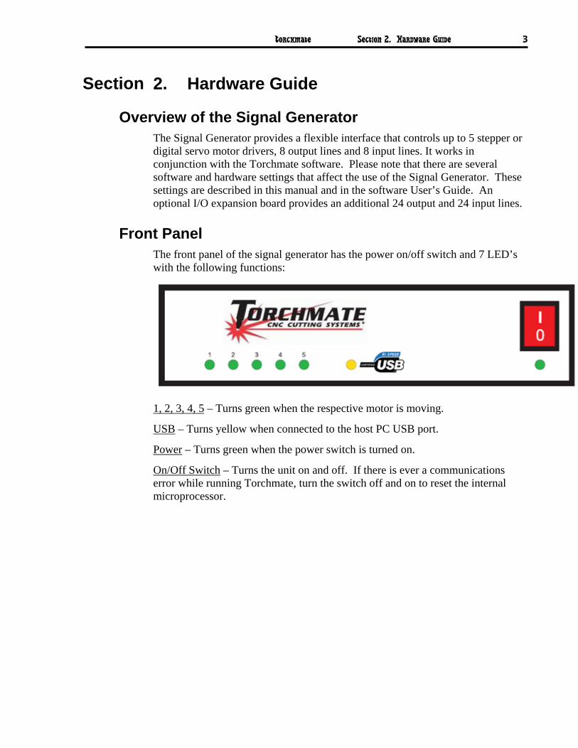
Front Panel The front panel of the signal generator has the power on/off switch and 7 LED’s with the following functions:
1, 2, 3, 4, 5 – Turns green when the respective motor is moving.
USB – Turns yellow when connected to the host PC USB port.
Power – Turns green when the power switch is turned on.
On/Off Switch – Turns the unit on and off. If there is ever a communications error while running Torchmate, turn the switch off and on to reset the internal microprocessor.
Section
Torchmate Section 2. Hardware Guide
4
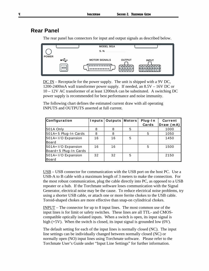
Rear Panel The rear panel has connectors for input and output signals as described below.
POWERMOTOR SIGNALS INPUTOUTPUT
MODEL 501A
S. N.
DC IN – Receptacle for the power supply. The unit is shipped with a 9V DC, 1200-2400mA wall transformer power supply. If needed, an 8.5V – 16V DC or 10 – 12V AC transformer of at least 1200mA can be substituted. A switching DC power supply is recommended for best performance and noise immunity.
The following chart defines the estimated current draw with all operating INPUTS and OUTPUTS asserted at full current.
Configuration Inputs Outputs Motors Plug-In Cards
Current Draw (mA)
501A Only 8 8 5 1000 501A+5 Plug-In Cards 8 8 5 1050 501A+I/O Expansion Board
16 16 5 1450
501A+I/O Expansion Board+5 Plug-In Cards
16 16 5 1500
501A+I/O Expansion Board
32 32 5 2150
USB – USB connector for communication with the USB port on the host PC. Use a USB-A to B cable with a maximum length of 3 meters to make the connection. For the most robust communication, plug the cable directly into PC, as opposed to a USB repeater or a hub. If the Torchmate software loses communication with the Signal Generator, electrical noise may be the cause. To reduce electrical noise problems, try using a shorter USB cable, or attach one or more ferrite chokes to the USB cable. Toroid-shaped chokes are more effective than snap-on cylindrical chokes.
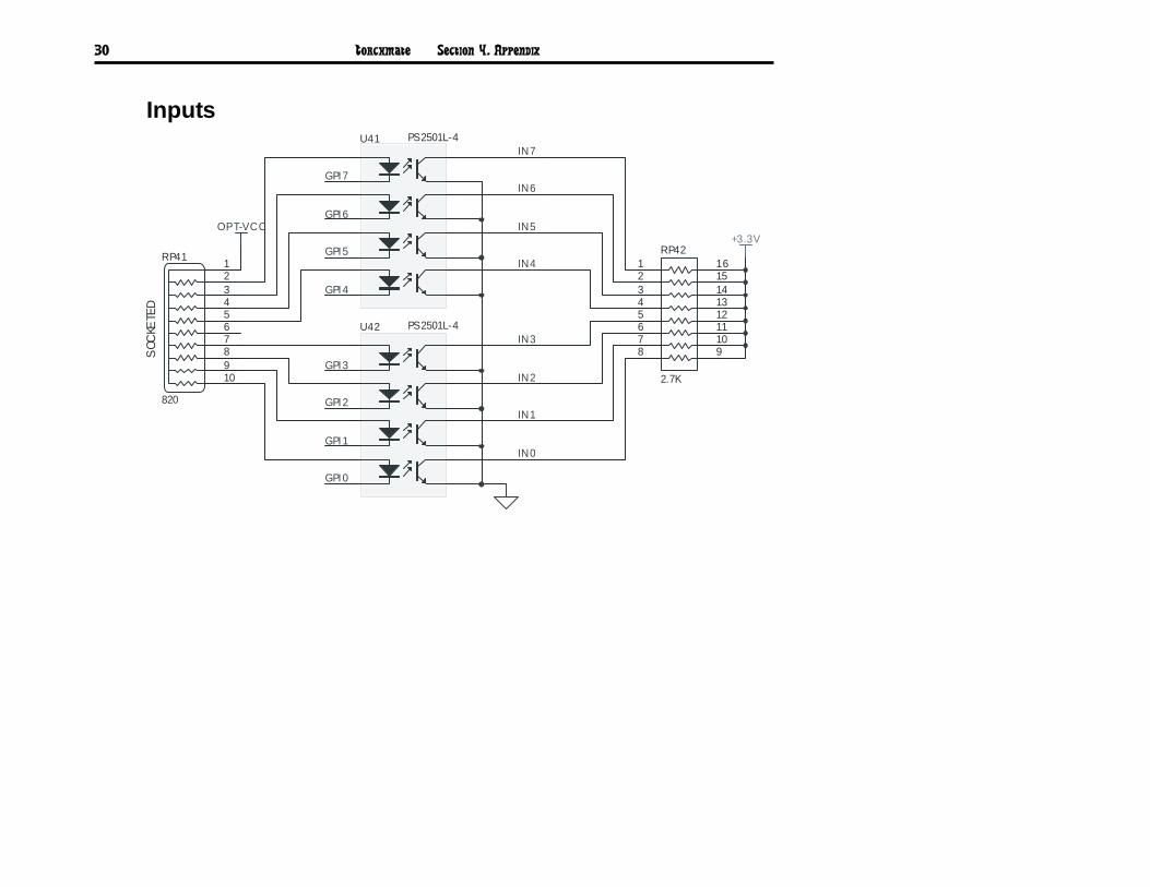
INPUT – The connector for up to 8 input lines. The most common use of the input lines is for limit or safety switches. These lines are all TTL- and CMOS-compatible optically isolated inputs. When a switch is open, its input signal is high (+5V). When the switch is closed, its input signal is grounded low (0V).
The default setting for each of the input lines is normally closed (NC). The input line settings can be individually changed between normally closed (NC) or normally open (NO) input lines using Torchmate software. Please refer to the Torchmate User’s Guide under “Input Line Settings” for further information.

Torchmate Section 2. Hardware Guide
5
In the Torchmate software, the Input Line Status dialog displays "OPEN" for a high-level input voltage, or open switch, and "CLOSED" for a low-level input voltage or closed switch.
The input lines are all optically isolated. Jumpers J84 and J85 enable you to choose between the internal power of the Signal Generator and isolated power from an external source. Both jumpers must be set on the same pair of pins (either both must be on pins 1 and 2 or both must be on pins 2 and 3).
• Internal Power
This is the most convenient option and works well for most applications, but negates some of the signal isolation. When JP84 shorts pins 1 and 2, OPT VCC gets its power from the Internal 5V power source. When JP85 shorts pins 1 and 2, OPT GND is directly connected to the Internal GND.
External Isolated Power
For the best noise immunity, connect an external 5V-24V power supply to the LED side of the optical couplers. When JP84 shorts pins 2 and 3, OPT VCC gets its optically isolated power from the TB-VCC. When JP85 shorts pins 2 and 3, OPT GND is directly connected to the TB-GND.
Choose only one of the following methods to supply power:
1. Connect a power source to the TB 40 screw terminal.
2. Connect a power source through pins 23 and 25 of the DB-25 connector.
If you are providing an external voltage through pins 23 and 25 of the DB25 Motor Signal connector or via TB-40, then you must have both JP84 and JP85 jump pins 2 and 3, OTHERWISE SEVERE DAMAGE COULD RESULT.
BE VERY CAREFUL WHEN DOING ANY WIRING. IMPROPER WIRING WILL DAMAGE THE SIGNAL GENERATOR.
Input lines 1, 2, 3 & 4 are also connected through pins 15, 16, 17 & 18 respectively of the Motor Signal connector, and input lines 5, 6, 7 & 8 are also connected through pins 5, 6, 7 & 8 respectively of the Motor Signal connector. This makes it convenient to send any signals from your motor driver box, such as limit lines or servo position error signal, back to the Signal Generator through the DB25 cable without using a separate input cable. Note that if an input line is being used through the Motor Signal connector, that line must remain open in the Input connector.
The receptacle that plugs into this connector is a Molex-Waldom Mini-Fit Jr. Series 16 pin receptacle (part number 39-01-2160), with female pins (part number 39-00-0039 or 39-00-0047 for 22 gauge or thinner wires).
The Molex 63811-1000 for 14-24 AWG universal or Molex 11-01-0197 Crimp Tools are recommended for installing the pins. Kits containing connectors and pins are available through Torchmate or an electronics distributor.

Torchmate Section 2. Hardware Guide
6
The input lines as seen from the back of the box are arranged as follows (all connections denoted by “OPT-GND” are optically isolated ground.):
Mini-Fit Jr. Pin No.
Signal Mini-Fit Jr. Pin No.
Signal
1 OPT-GND 9 INPUT 1 2 OPT-GND 10 INPUT 2 3 OPT-GND 11 INPUT 3 4 OPT-GND 12 INPUT 4 5 OPT-GND 13 INPUT 5 6 OPT-GND 14 INPUT 6 7 OPT-GND 15 INPUT 7 8 OPT-GND 16 INPUT 8
OUTPUT – The connector for up to 8 output lines. These lines are all compatible with TTL/CMOS level outputs. The Output ports are not setup to drive a 24V external system unless it accepts TTL/CMOS levels. They are all driven by HCT family logic. Output logic high is normally 5V and can go down to 3.9V at full load. Output logic low is normally 0V and can go up to 0.3V at full load. Each of these signals can provide up to 20mA of current.
Two additional pins on this connector are provided for your output lines: ground and +5V. These are connected to GND and +5V and are not optically isolated. This 5V circuit can source up to 100 mA. Any larger current demand would require a larger power source.
BE VERY CAREFUL WHEN DOING ANY WIRING. IMPROPER WIRING WILL DAMAGE THE SIGNAL GENERATOR.
The output lines are all initialized to low (0V) when you turn on the Signal Generator. Output lines 1 and 2 are also connected through pins 1 and 2 respectively of the Motor Signal connector. This makes it convenient to connect up to 2 output signals to your motor driver box to drive devices such as solid-state relays that might be in your motor driver box.
The receptacle that plugs into this connector is a Molex-Waldom Mini-Fit Jr. Series 10 pin receptacle (part number 39-01-2100), with female pins (part number 39-00-0039 or 39-00-0047 for 22 gauge or thinner wires).
The Molex 63811-1000 for 14-24 AWG universal or Molex 11-01-0197 Crimp Tools are recommended for installing the pins. Kits containing connectors and pins are available through Torchmate or an electronics distributor.
The output lines as seen from the back of the box are arranged as follows:
16 15 14 13 12 11 10 9 8 7 6 5 4 3 2 1
Torchmate Section 2. Hardware Guide
7
Mini-Fit Jr. Pin No.
Signal Mini-Fit Jr. Pin No.
Signal
1 OUTPUT 1 6 OUTPUT 2 2 OUTPUT 3 7 OUTPUT 4 3 OUTPUT 5 8 OUTPUT 6 4 OUTPUT 7 9 OUTPUT 8 5 +5V 10 GROUND
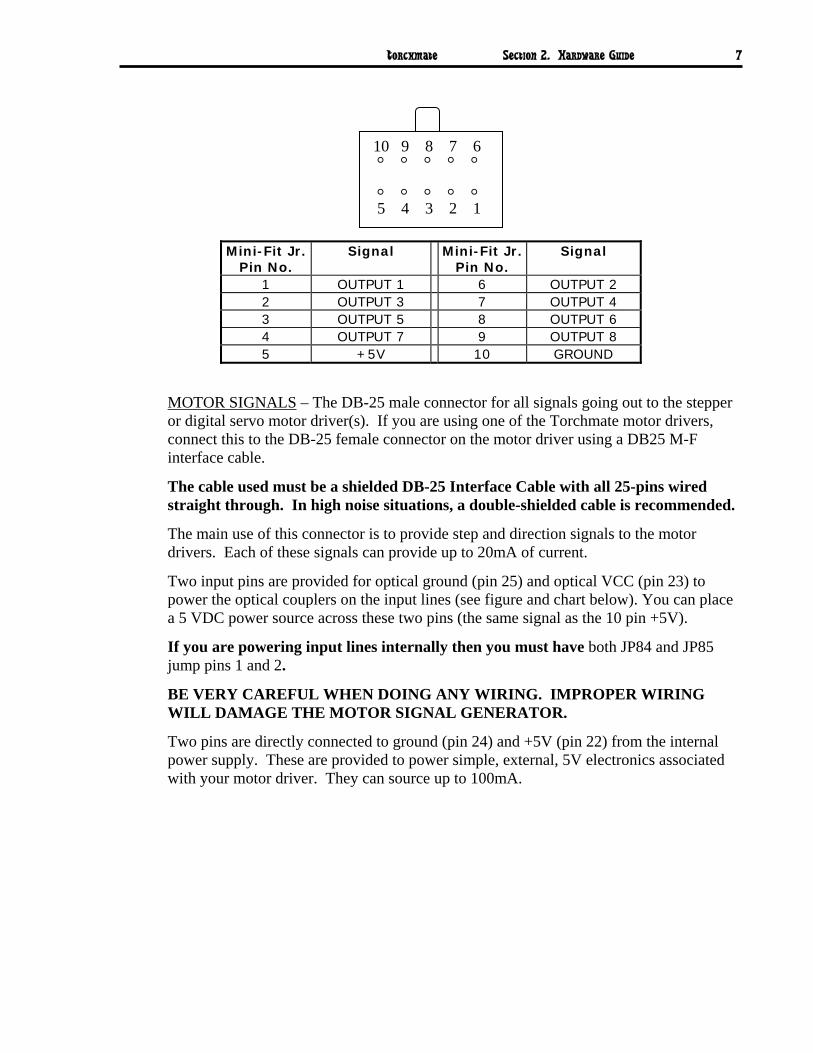
MOTOR SIGNALS – The DB-25 male connector for all signals going out to the stepper or digital servo motor driver(s). If you are using one of the Torchmate motor drivers, connect this to the DB-25 female connector on the motor driver using a DB25 M-F interface cable.
The cable used must be a shielded DB-25 Interface Cable with all 25-pins wired straight through. In high noise situations, a double-shielded cable is recommended.
The main use of this connector is to provide step and direction signals to the motor drivers. Each of these signals can provide up to 20mA of current.
Two input pins are provided for optical ground (pin 25) and optical VCC (pin 23) to power the optical couplers on the input lines (see figure and chart below). You can place a 5 VDC power source across these two pins (the same signal as the 10 pin +5V).
If you are powering input lines internally then you must have both JP84 and JP85 jump pins 1 and 2.
BE VERY CAREFUL WHEN DOING ANY WIRING. IMPROPER WIRING WILL DAMAGE THE MOTOR SIGNAL GENERATOR.
Two pins are directly connected to ground (pin 24) and +5V (pin 22) from the internal power supply. These are provided to power simple, external, 5V electronics associated with your motor driver. They can source up to 100mA.
10 9 8 7 6 5 4 3 2 1

Torchmate Section 2. Hardware Guide
8
The motor signal lines as seen from the back of the box are arranged as follows:
1 13
14 25
DB25 Pin No.
Signal DB25 Pin No.
Signal
1 OUTPUT 1 14 ENABLE ALL 2 OUTPUT 2 15 INPUT 1 3 STEP AXIS 5 16 INPUT 2 4 DIRECTION AXIS 5 17 INPUT 3 5 INPUT 5 18 INPUT 4 6 INPUT 6 19 DIRECTION AXIS 4 7 INPUT 7 20 DIRECTION AXIS 3 8 INPUT 8 21 DIRECTION AXIS 2 9 DIRECTION AXIS 1 22 Internal VCC +5V 10 STEP AXIS 4 23 OPT VCC (INPUT) 11 STEP AXIS 3 24 Internal GND 12 STEP AXIS 2 25 OPT GND (INPUT) 13 STEP AXIS 1
Removing the Signal Generator Top Cover To remove the cover from the unit, turn the unit over and remove all 4 of the screws. Then flip the unit back over and lift the top cover off.
Jumper Settings Pin 1 of all jumpers is indicated by a small white dot printed on the PCB.
JP83 – Chassis Ground This connects the internal signal ground of the Signal Generator to the chassis ground. Always leave open unless directed otherwise by Torchmate technical support.
Torchmate Section 2. Hardware Guide
9
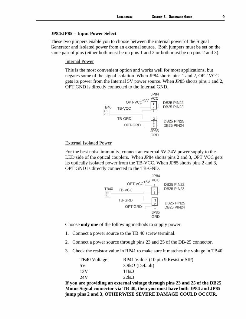
JP84/JP85 – Input Power Select These two jumpers enable you to choose between the internal power of the Signal Generator and isolated power from an external source. Both jumpers must be set on the same pair of pins (either both must be on pins 1 and 2 or both must be on pins 2 and 3).
Internal Power
This is the most convenient option and works well for most applications, but negates some of the signal isolation. When JP84 shorts pins 1 and 2, OPT VCC gets its power from the Internal 5V power source. When JP85 shorts pins 1 and 2, OPT GND is directly connected to the Internal GND.
DB25 PIN22DB25 PIN23
DB25 PIN24DB25 PIN25
TB40
OPT-GRD
TB-VCCOPT-VCC
TB-GRD
+5V123
JP84VCC
JP85GRD
12
3 2 1
External Isolated Power
For the best noise immunity, connect an external 5V-24V power supply to the LED side of the optical couplers. When JP84 shorts pins 2 and 3, OPT VCC gets its optically isolated power from the TB-VCC. When JP85 shorts pins 2 and 3, OPT GND is directly connected to the TB-GND.
DB25 PIN22DB25 PIN23
DB25 PIN24DB25 PIN25
OPT-GRD
TB-VCCOPT-VCC
TB-GRD
+5V123
JP84VCC
JP85GRD
3 2 1
Choose only one of the following methods to supply power:
1. Connect a power source to the TB 40 screw terminal.
2. Connect a power source through pins 23 and 25 of the DB-25 connector.
3. Check the resistor value in RP41 to make sure it matches the voltage in TB40.
TB40 Voltage RP41 Value (10 pin 9 Resistor SIP) 5V 3.9kΩ (Default) 12V 11kΩ 24V 22kΩ
If you are providing an external voltage through pins 23 and 25 of the DB25 Motor Signal connector via TB-40, then you must have both JP84 and JP85 jump pins 2 and 3, OTHERWISE SEVERE DAMAGE COULD OCCUR.
Torchmate Section 2. Hardware Guide
10
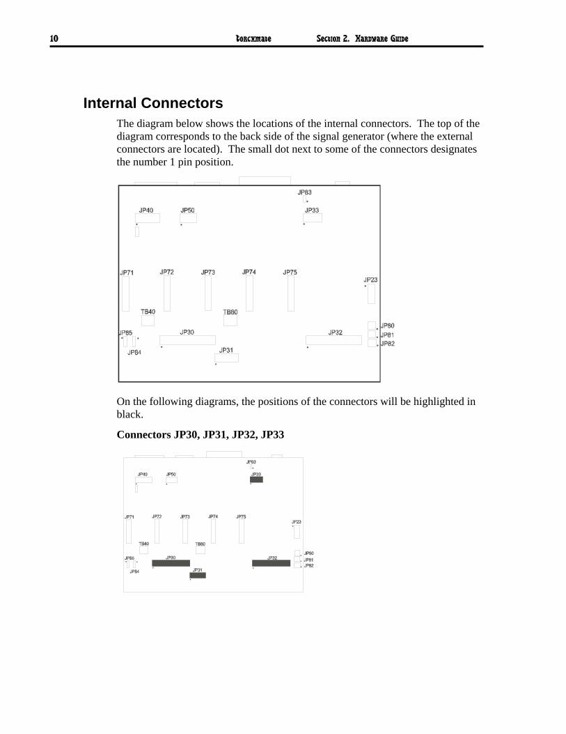
Internal Connectors The diagram below shows the locations of the internal connectors. The top of the diagram corresponds to the back side of the signal generator (where the external connectors are located). The small dot next to some of the connectors designates the number 1 pin position.
On the following diagrams, the positions of the connectors will be highlighted in black.
Connectors JP30, JP31, JP32, JP33
Torchmate Section 2. Hardware Guide
11
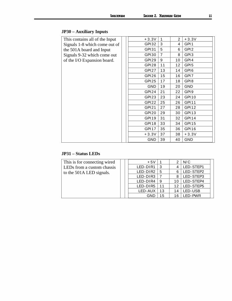
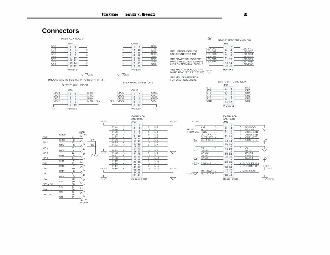
JP30 – Auxiliary Inputs
This contains all of the Input Signals 1-8 which come out of the 501A board and Input Signals 9-32 which come out of the I/O Expansion board.
+3.3V 1 2 +3.3V GPI32 3 4 GPI1 GPI31 5 6 GPI2 GPI30 7 8 GPI3 GPI29 9 10 GPI4 GPI28 11 12 GPI5 GPI27 13 14 GPI6 GPI26 15 16 GPI7 GPI25 17 18 GPI8
GND 19 20 GND GPI24 21 22 GPI9 GPI23 23 24 GPI10 GPI22 25 26 GPI11 GPI21 27 28 GPI12 GPI20 29 30 GPI13 GPI19 31 32 GPI14 GPI18 33 34 GPI15 GPI17 35 36 GPI16 +3.3V 37 38 +3.3V
GND 39 40 GND
JP31 – Status LEDs
This is for connecting wired LEDs from a custom chassis to the 501A LED signals.
+5V 1 2 N/C LED-DIR1 3 4 LED-STEP1 LED-DIR2 5 6 LED-STEP2 LED-DIR3 7 8 LED-STEP3 LED-DIR4 9 10 LED-STEP4 LED-DIR5 11 12 LED-STEP5 LED-AUX 13 14 LED-USB
GND 15 16 LED-PWR

Torchmate Section 2. Hardware Guide
12
JP32 – Bus Expansion
This contains signal and address lines for the I/O Expansion board.
+3.3V 1 2 GND CS6 3 4 STATUS6
TXD2 5 6 FAULT6 RXD2 7 8 AUX1-STB
OUT-ENA 9 10 AUX2-STB OUT2-STB 11 12 OUT1-STB OUT4-STB 13 14 OUT3-STB
+5V 15 16 +5V GND 17 18 GND
A0 19 20 A1 DATA1 21 22 DATA2 DATA3 23 24 DATA4 DATA8 25 26 DATA7 DATA6 27 28 DATA5
+7V 29 30 +7V SPHOME 31 32 ENC CLK
+3.3V 33 34 ENC DIR AGND 35 36 AV+ DAC2 37 38 DAC1 ADC1 39 40 AGND
JP33 – Step & Direction
This contains all of the step and direction signals for 5 axes of motion.
STEP5 1 2 ENA STEP4 3 4 DIR5 STEP3 5 6 DIR4 STEP2 7 8 DIR3 STEP1 9 10 DIR2
GND 11 12 DIR1
Torchmate Section 2. Hardware Guide
13
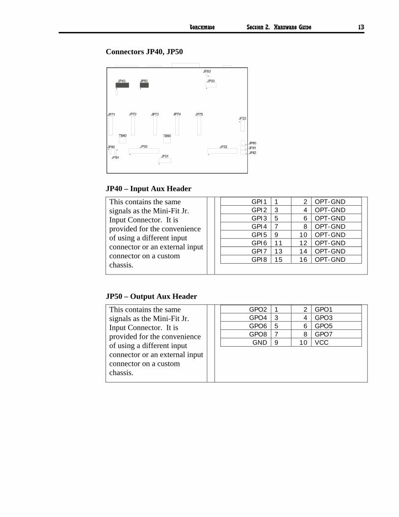
Connectors JP40, JP50
JP40 – Input Aux Header
This contains the same signals as the Mini-Fit Jr. Input Connector. It is provided for the convenience of using a different input connector or an external input connector on a custom chassis.
GPI1 1 2 OPT-GND GPI2 3 4 OPT-GND GPI3 5 6 OPT-GND GPI4 7 8 OPT-GND GPI5 9 10 OPT-GND GPI6 11 12 OPT-GND GPI7 13 14 OPT-GND GPI8 15 16 OPT-GND
JP50 – Output Aux Header
This contains the same signals as the Mini-Fit Jr. Input Connector. It is provided for the convenience of using a different input connector or an external input connector on a custom chassis.
GPO2 1 2 GPO1 GPO4 3 4 GPO3 GPO6 5 6 GPO5 GPO8 7 8 GPO7 GND 9 10 VCC

Torchmate Section 2. Hardware Guide
14
Connectors JP80, JP81, JP82
JP80 – Rear Panel Power Connect the main power here. It can be 8.5V – 16V DC or AC. See current draw chart for power requirements.
JP81 – Rear Panel Fuse This is for an optional power fuse. The unit is shipped with a shunt instead of a fuse. If you replace the shunt with a fuse, it should be sized according to your power requirements.
JP82 – Front Panel Switch
Connect the main power switch here.
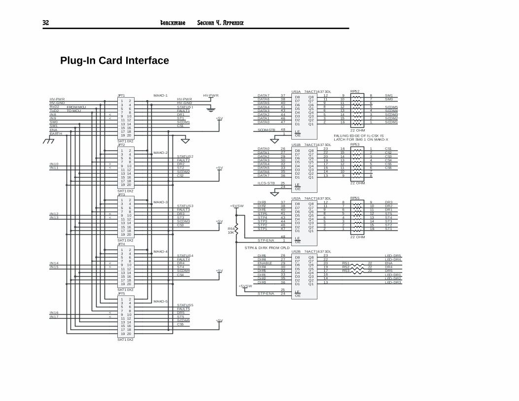
Plug-In Card Interfaces Plug-In Cards JP71 – JP75
The plug-in card interfaces are used to add additional functions to the main signal generator board. For example, a stepper drive plug-in card will enable you to drive a stepper motor directly from the signal generator box.
Torchmate Section 2. Hardware Guide
15
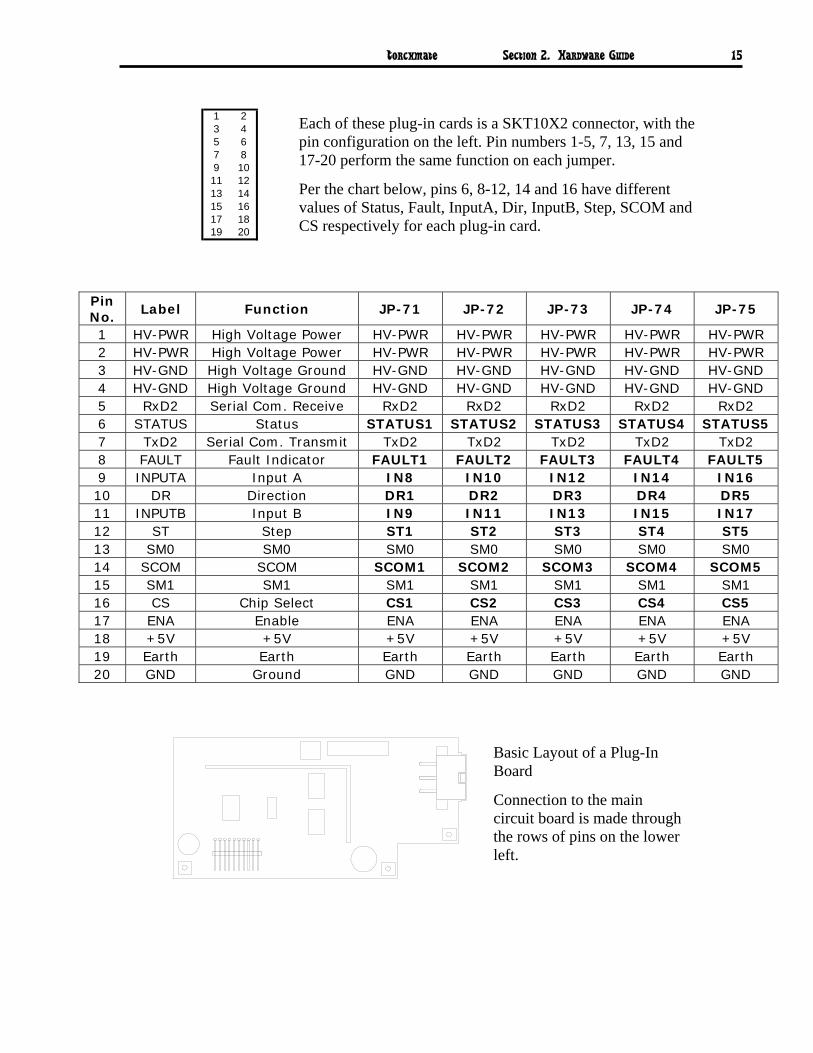
1 23 45 67 89 10
11 1213 1415 1617 1819 20
Each of these plug-in cards is a SKT10X2 connector, with the pin configuration on the left. Pin numbers 1-5, 7, 13, 15 and 17-20 perform the same function on each jumper.
Per the chart below, pins 6, 8-12, 14 and 16 have different values of Status, Fault, InputA, Dir, InputB, Step, SCOM and CS respectively for each plug-in card.
Basic Layout of a Plug-In Board
Connection to the main circuit board is made through the rows of pins on the lower left.
Pin No.
Label Function JP-71 JP-72 JP-73 JP-74 JP-75
1 HV-PWR High Voltage Power HV-PWR HV-PWR HV-PWR HV-PWR HV-PWR 2 HV-PWR High Voltage Power HV-PWR HV-PWR HV-PWR HV-PWR HV-PWR 3 HV-GND High Voltage Ground HV-GND HV-GND HV-GND HV-GND HV-GND 4 HV-GND High Voltage Ground HV-GND HV-GND HV-GND HV-GND HV-GND 5 RxD2 Serial Com. Receive RxD2 RxD2 RxD2 RxD2 RxD2 6 STATUS Status STATUS1 STATUS2 STATUS3 STATUS4 STATUS5 7 TxD2 Serial Com. Transmit TxD2 TxD2 TxD2 TxD2 TxD2 8 FAULT Fault Indicator FAULT1 FAULT2 FAULT3 FAULT4 FAULT5 9 INPUTA Input A IN8 IN10 IN12 IN14 IN16 10 DR Direction DR1 DR2 DR3 DR4 DR5 11 INPUTB Input B IN9 IN11 IN13 IN15 IN17 12 ST Step ST1 ST2 ST3 ST4 ST5 13 SM0 SM0 SM0 SM0 SM0 SM0 SM0 14 SCOM SCOM SCOM1 SCOM2 SCOM3 SCOM4 SCOM5 15 SM1 SM1 SM1 SM1 SM1 SM1 SM1 16 CS Chip Select CS1 CS2 CS3 CS4 CS5 17 ENA Enable ENA ENA ENA ENA ENA 18 +5V +5V +5V +5V +5V +5V +5V 19 Earth Earth Earth Earth Earth Earth Earth 20 GND Ground GND GND GND GND GND


Torchmate Section 3. Wiring Diagrams
17
3. Sample Wiring Diagrams Section
Torchmate Section 3. Wiring Diagrams
18
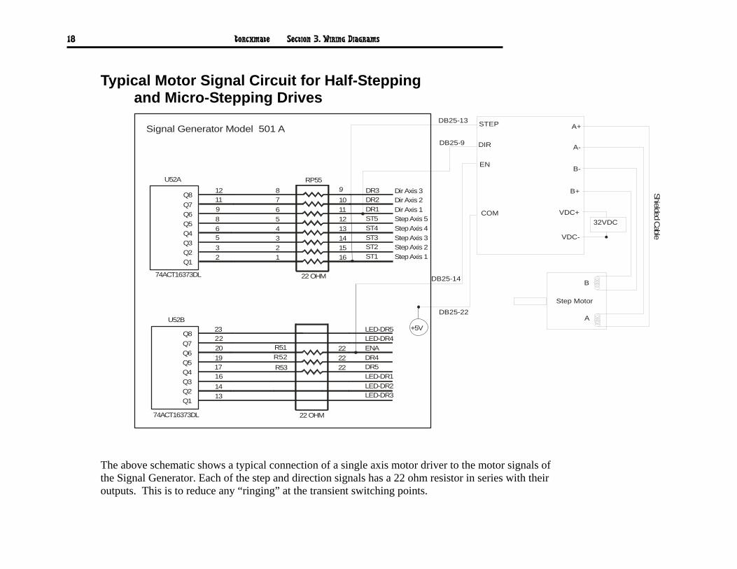
Typical Motor Signal Circuit for Half-Stepping and Micro-Stepping Drives
Signal Generator Model 501 A
DB25-22
STEP
COM
EN
DIR
A+
A-
B-
B+
VDC+
VDC-
32VDC
Shielded Cable
1514131211109
Q7
74ACT16373DL
Q1Q2Q3Q4Q5Q6
5
23
86
9
22 OHM
3
12
54
6
16
U52A
Q81211
RP5587
ST3
ST1ST2
ST4ST5DR1DR2DR3
Step Axis 2Step Axis 1
Step Axis 4Step Axis 3
Step Axis 5
Dir Axis 2Dir Axis 1
Dir Axis 3
+5V
222222
Q7
74ACT16373DL
Q1Q2Q3Q4Q5Q6
16
1314
1917
20
22 OHM
R51
R53
U52B
Q82322
LED-DR1
LED-DR3LED-DR2
DR5DR4ENALED-DR4LED-DR5
R52
Step Motor
B
A
DB25-9
DB25-13
DB25-14
The above schematic shows a typical connection of a single axis motor driver to the motor signals of the Signal Generator. Each of the step and direction signals has a 22 ohm resistor in series with their outputs. This is to reduce any “ringing” at the transient switching points.
Torchmate Section 3. Wiring Diagrams
19
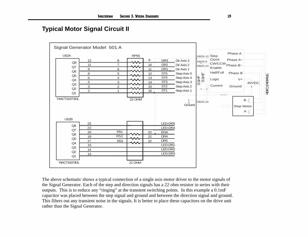
Typical Motor Signal Circuit II
Signal Generator Model 501 A
1514131211109
Q7
74ACT16373DL
Q1Q2Q3Q4Q5Q6
5
23
86
9
22 OHM
3
12
54
6
16
U52A
Q81211
RP5587
ST3
ST1ST2
ST4ST5DR1DR2DR3
Step Axis 2Step Axis 1
Step Axis 4Step Axis 3
Step Axis 5
Dir Axis 2Dir Axis 1
Dir Axis 3
222222
Q7
74ACT16373DL
Q1Q2Q3Q4Q5Q6
16
1314
1917
20
22 OHM
R51
R53
U52B
Q82322
LED-DR1
LED-DR3LED-DR2
DR5DR4ENALED-DR4LED-DR5
R52
Step Clock
Logic
EnableHalf/Full
CW/CCW
0.1m
F0.
1mF
Phase A
Phase A~
Phase B~
Phase B
V+
Ground40VDC
Shielded Cable
Current
Ground Step Motor
B
A
DB25-14
DB25-24
DB25-13
DB25-9
The above schematic shows a typical connection of a single axis motor driver to the motor signals of the Signal Generator. Each of the step and direction signals has a 22 ohm resistor in series with their outputs. This is to reduce any “ringing” at the transient switching points. In this example a 0.1mF capacitor was placed between the step signal and ground and between the direction signal and ground. This filters out any transient noise in the signals. It is better to place these capacitors on the drive unit rather than the Signal Generator.
Torchmate Section 3. Wiring Diagrams
20
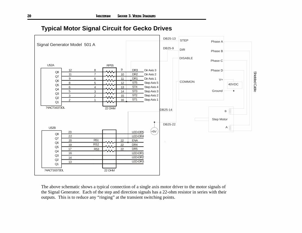
Typical Motor Signal Circuit for Gecko Drives
Signal Generator Model 501 A
DB25-22
STEP
COMMON
DISABLE
DIR
Phase A
Phase B
Phase C
Phase D
V+
Ground
40VDC
Shielded Cable
1514131211109
Q7
74ACT16373DL
Q1Q2Q3Q4Q5Q6
5
23
86
9
22 OHM
3
12
54
6
16
U52A
Q81211
RP5587
ST3
ST1ST2
ST4ST5DR1DR2DR3
Step Axis 2Step Axis 1
Step Axis 4Step Axis 3
Step Axis 5
Dir Axis 2Dir Axis 1
Dir Axis 3
+5V
222222
Q7
74ACT16373DL
Q1Q2Q3Q4Q5Q6
16
1314
1917
20
22 OHM
R51
R53
U52B
Q82322
LED-DR1
LED-DR3LED-DR2
DR5DR4ENALED-DR4LED-DR5
R52S
Step Motor
A
B
DB25-13
DB25-9
DB25-14
The above schematic shows a typical connection of a single axis motor driver to the motor signals of the Signal Generator. Each of the step and direction signals has a 22-ohm resistor in series with their outputs. This is to reduce any “ringing” at the transient switching points.
Torchmate Section 3. Wiring Diagrams
21
Typical Output Line Circuit
Signal Generator Model 501A
Solid State Relay Continental Industries S505-0SJ610-000
+ 3
Load
1
2
AC Fuse
3.3K
4
OPT
GND
Output1
74ACT16373DL
Q8
U50A
Q1
Q4
Q6Q7
Q5
Q3Q2
GPO7GPO6GPO5GPO4GPO3GPO2GPO1GPO0
22 OHM
11
910
1312
14
R 51P1615
Output Line 1
Output Line 8
Output Line 5
Output Line 7Output Line 6
Output Line 3Output Line 4
Output Line 2
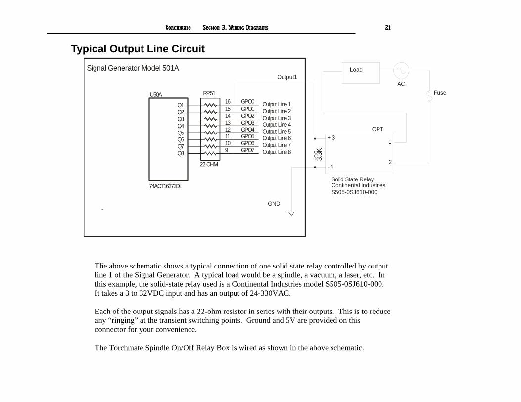
The above schematic shows a typical connection of one solid state relay controlled by output line 1 of the Signal Generator. A typical load would be a spindle, a vacuum, a laser, etc. In this example, the solid-state relay used is a Continental Industries model S505-0SJ610-000. It takes a 3 to 32VDC input and has an output of 24-330VAC. Each of the output signals has a 22-ohm resistor in series with their outputs. This is to reduce any “ringing” at the transient switching points. Ground and 5V are provided on this connector for your convenience. The Torchmate Spindle On/Off Relay Box is wired as shown in the above schematic.
Torchmate Section 3. Wiring Diagrams
22
Typical Input Line Circuit – Internal Power
Input 8
Input 7
Input 6Input 5
Input 4
Input 3Input 2
Input 1
Signal Generator Model 501 A
DB25 Pin8DB25 Pin7DB25 Pin6DB25 Pin5DB25 Pin18DB25 Pin17DB25 Pin16
DB25 Pin15
OPT
GND
OPT GND
NC-NO
U42
OPT_VCC
RP41
GPI0GPI1
GPI2GPI3
820
PS2501L-4
IN0IN1
IN2IN3
GPI4
GPI5GPI6
GPI7
PS2501L-4
U41
VCC
IN4IN5
IN6
2.7K
81 2 3 64 5 7
RP42
IN7
DB25 PIN22DB25 PIN23
DB25 PIN24DB25 PIN25
621 43 5 1087 9
TB40
OPT-GRD
TB-VCC
OPT-VCC
TB-GRD
+5V123
JP84VCC
JP85GRD
12
3 2 1
9 10
Torchmate Section 3. Wiring Diagrams
23
Typical Input Line Circuit – External Power
Input 8
Input 7
Input 6Input 5
Input 4
Input 3Input 2
Input 1
Signal Generator Model 501 A
DB25 Pin8DB25 Pin7DB25 Pin6DB25 Pin5DB25 Pin18DB25 Pin17DB25 Pin16
DB25 Pin15
OPT
GND
OPT GND
NC-NO
U42
OPT_VCC
RP41
GPI0GPI1
GPI2GPI3
820
PS2501L-4
IN0IN1
IN2IN3
GPI4
GPI5GPI6
GPI7
PS2501L-4
U41
VCC
IN4IN5
IN6
2.7K
81 2 3 64 5 7
RP42
IN7
DB25 PIN22DB25 PIN23
DB25 PIN24DB25 PIN25
621 43 5 1087 9
TB40
OPT-GRD
TB-VCC
OPT-VCC
TB-GRD
+5V123
JP84VCC
JP85GRD
12
3 2 1
9 10

Torchmate Section 3. Wiring Diagrams
24
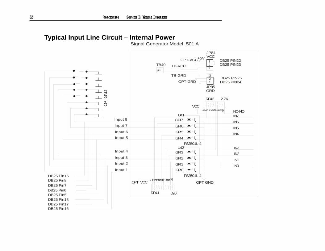
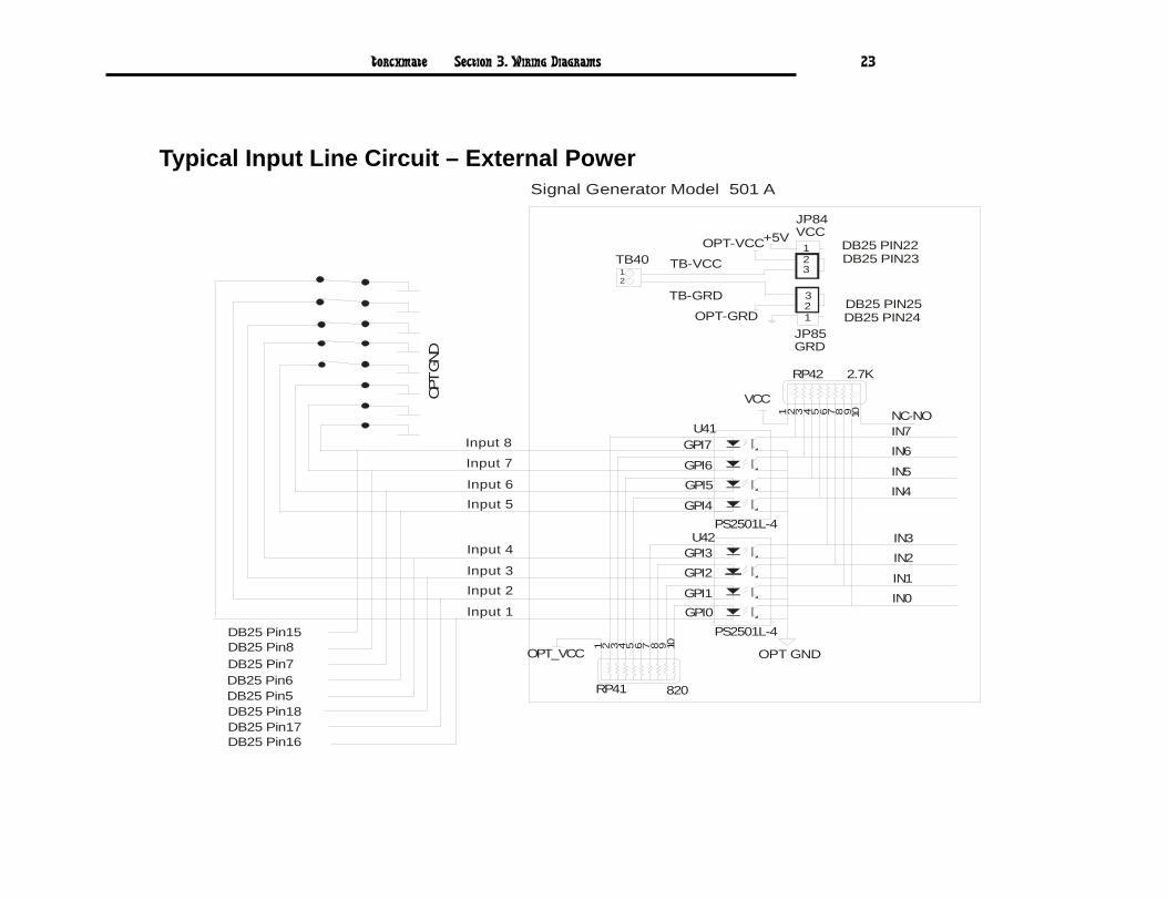
The above schematic shows a typical connection of 5 normally closed switches. These switches are connected between input lines 1-5 and ground. Lines 6-8 are connected directly to ground with jumper wires. All external connections shown are made through the Input connector on the back of the Signal Generator. This resistor pack (RP41) is socketed so that you can change the value if needed for your application. The input lines are all optically isolated. In this example, JP84 and JP85 are shorted using the internal power to source the external side of the optical couplers. However, for the best isolation, JP84 and JP85 should be open, and power should be provided through pins 23 and 25 of the DB25 Motor Signal connector. Input lines 1-4 and 5- 8 are internally connected to pins 15-18 and 5-8 respectively of the DB25 Motor Signal connector. Note that the Torchmate limit switch kit has the same wiring as shown in this example.
Torchmate Section 4. Appendix
25
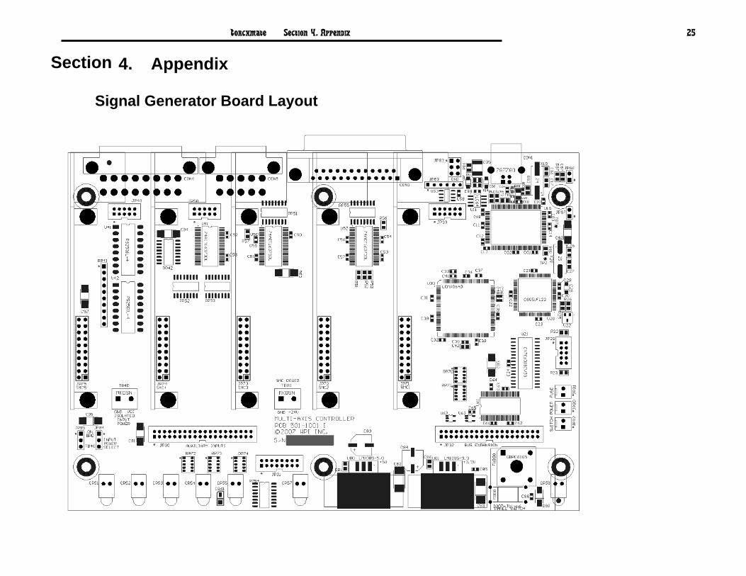
4. Appendix Signal Generator Board Layout
Section
Torchmate Section 4. Appendix
26
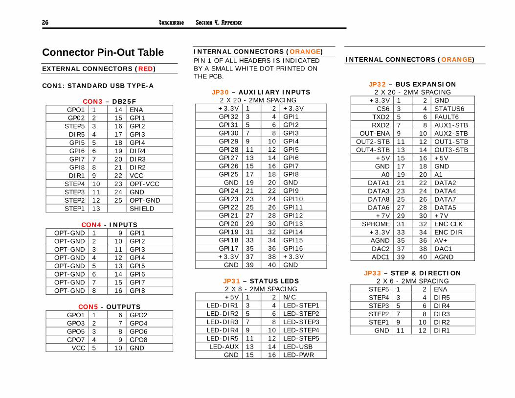
Connector Pin-Out Table
EXTERNAL CONNECTORS (RED) CON1: STANDARD USB TYPE-A
CON3 – DB25F GPO1 1 14 ENA GP02 2 15 GPI1
STEP5 3 16 GPI2 DIR5 4 17 GPI3 GPI5 5 18 GPI4 GPI6 6 19 DIR4 GPI7 7 20 DIR3 GPI8 8 21 DIR2 DIR1 9 22 VCC
STEP4 10 23 OPT-VCC STEP3 11 24 GND STEP2 12 25 OPT-GND STEP1 13 SHIELD
CON4 - INPUTS
OPT-GND 1 9 GPI1 OPT-GND 2 10 GPI2 OPT-GND 3 11 GPI3 OPT-GND 4 12 GPI4 OPT-GND 5 13 GPI5 OPT-GND 6 14 GPI6 OPT-GND 7 15 GPI7 OPT-GND 8 16 GPI8
CON5 - OUTPUTS
GPO1 1 6 GPO2 GPO3 2 7 GPO4 GPO5 3 8 GPO6 GPO7 4 9 GPO8
VCC 5 10 GND
INTERNAL CONNECTORS (ORANGE) PIN 1 OF ALL HEADERS IS INDICATED BY A SMALL WHITE DOT PRINTED ON THE PCB.
JP30 – AUXILIARY INPUTS 2 X 20 - 2MM SPACING +3.3V 1 2 +3.3V GPI32 3 4 GPI1 GPI31 5 6 GPI2 GPI30 7 8 GPI3 GPI29 9 10 GPI4 GPI28 11 12 GPI5 GPI27 13 14 GPI6 GPI26 15 16 GPI7 GPI25 17 18 GPI8
GND 19 20 GND GPI24 21 22 GPI9 GPI23 23 24 GPI10 GPI22 25 26 GPI11 GPI21 27 28 GPI12 GPI20 29 30 GPI13 GPI19 31 32 GPI14 GPI18 33 34 GPI15 GPI17 35 36 GPI16 +3.3V 37 38 +3.3V
GND 39 40 GND
JP31 – STATUS LEDS 2 X 8 - 2MM SPACING +5V 1 2 N/C
LED-DIR1 3 4 LED-STEP1 LED-DIR2 5 6 LED-STEP2 LED-DIR3 7 8 LED-STEP3 LED-DIR4 9 10 LED-STEP4 LED-DIR5 11 12 LED-STEP5 LED-AUX 13 14 LED-USB
GND 15 16 LED-PWR
INTERNAL CONNECTORS (ORANGE)
JP32 – BUS EXPANSION
2 X 20 - 2MM SPACING +3.3V 1 2 GND
CS6 3 4 STATUS6 TXD2 5 6 FAULT6 RXD2 7 8 AUX1-STB
OUT-ENA 9 10 AUX2-STB OUT2-STB 11 12 OUT1-STB OUT4-STB 13 14 OUT3-STB
+5V 15 16 +5V GND 17 18 GND
A0 19 20 A1 DATA1 21 22 DATA2 DATA3 23 24 DATA4 DATA8 25 26 DATA7 DATA6 27 28 DATA5
+7V 29 30 +7V SPHOME 31 32 ENC CLK
+3.3V 33 34 ENC DIR AGND 35 36 AV+ DAC2 37 38 DAC1 ADC1 39 40 AGND
JP33 – STEP & DIRECTION
2 X 6 - 2MM SPACING STEP5 1 2 ENA STEP4 3 4 DIR5 STEP3 5 6 DIR4 STEP2 7 8 DIR3 STEP1 9 10 DIR2
GND 11 12 DIR1
Torchmate Section 4. Appendix
27
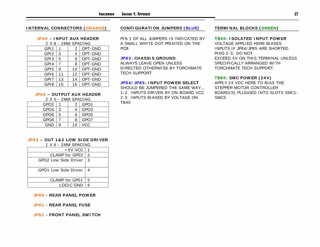
INTERNAL CONNECTORS (ORANGE)
JP40 – INPUT AUX HEADER
2 X 8 - 2MM SPACING GPI1 1 2 OPT-GND GPI2 3 4 OPT-GND GPI3 5 6 OPT-GND GPI4 7 8 OPT-GND GPI5 9 10 OPT-GND GPI6 11 12 OPT-GND GPI7 13 14 OPT-GND GPI8 15 16 OPT-GND
JP50 – OUTPUT AUX HEADER
2 X 5 - 2MM SPACING GPO2 1 2 GPO1 GPO4 3 4 GPO3 GPO6 5 6 GPO5 GPO8 7 8 GPO7 GND 9 10 VCC
JP53 – OUT 1&2 LOW SIDE DRIVER
1 X 6 - 2MM SPACING +5V VCC 1
CLAMP for GP02 2 GPO2 Low Side Driver 3
GPO1 Low Side Driver 4
CLAMP for GP01 5 LOGIC GND 6
JP80 - REAR PANEL POWER JP81 - REAR PANEL FUSE JP82 - FRONT PANEL SWITCH
CONFIGURATION JUMPERS (BLUE) PIN 1 OF ALL JUMPERS IS INDICATED BY A SMALL WHITE DOT PRINTED ON THE PCB. JP83: CHASSIS GROUND ALWAYS LEAVE OPEN UNLESS DIRECTED OTHERWISE BY TORCHMATE TECH SUPPORT JP84/JP85: INPUT POWER SELECT SHOULD BE JUMPERED THE SAME WAY… 1-2: INPUTS DRIVEN BY ON-BOARD VCC 2-3: INPUTS BIASED BY VOLTAGE ON TB40
TERMINAL BLOCKS (GREEN) TB40: ISOLATED INPUT POWER VOLTAGE APPLIED HERE BIASES INPUTS IF JP84/JP85 ARE SHORTED PINS 2-3; DO NOT EXCEED 5V ON THIS TERMINAL UNLESS SPECIFICALLY ARRANGED WITH TORCHMATE TECH SUPPORT. TB80: SMC POWER (24V) APPLY 24 VDC HERE TO BIAS THE STEPPER MOTOR CONTROLLER BOARD(S) PLUGGED INTO SLOTS SMC1-SMC5
Torchmate Section 4. Appendix
28
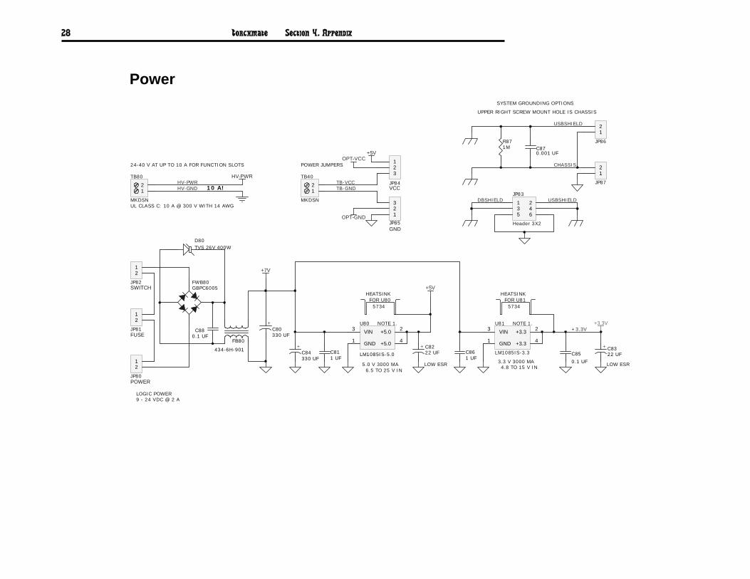
Power
+3.3V
3.3 V 3000 MA
12
TB80
MKDSN
LOGIC POWER
4.8 TO 15 V IN
HV-PWRHV-GND
CHASSIS
HV-PWR
24-40 V AT UP TO 10 A FOR FUNCTION SLOTS
+5V
VCC
GND
POWER JUMPERS
UL CLASS C: 10 A @ 300 V WITH 14 AWG
12
JP8710 A!
+5V
6.5 TO 25 V IN5.0 V 3000 MA
9 - 24 VDC @ 2 A
LOW ESR LOW ESR
C85
0.1 UF
+ C8222 UF
+ C8322 UF
12
JP80
D80TVS 26V 400W
12
JP81FUSE
POWER
12
JP82SWITCH
+7V
+3.3VVIN3 +5.0 2
+5.0 4GND1
U80
LM1085IS-5.0
FWB80GBPC6005
12
TB40
MKDSN
TB-VCCTB-GND
OPT-VCC
OPT-GND
NOTE 1.
FB80
434-6H-901
123
JP84
123
JP85
VIN3 +3.3 2
+3.3 4GND1
U81
LM1085IS-3.3
NOTE 1.
UPPER RIGHT SCREW MOUNT HOLE IS CHASSIS
FOR U805734
FOR U815734
HEATSINK HEATSINK
+C80330 UF
C861 UF
+C84330 UF
C811 UF
1 23 45 6
JP83
Header 3X2
USBSHIELD
12
JP86
DBSHIELD USBSHIELD
SYSTEM GROUNDING OPTIONS
C870.001 UF
R871M
C880.1 UF
Torchmate Section 4. Appendix
29
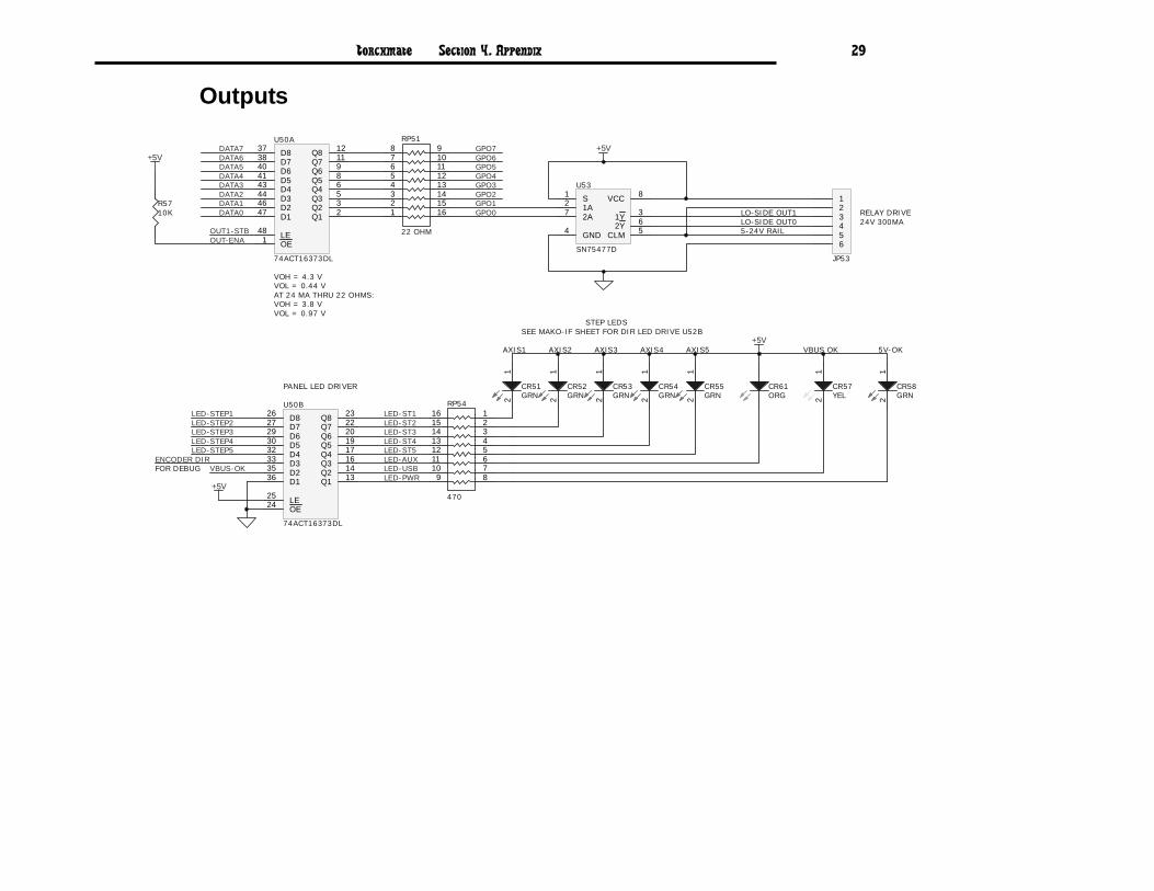
Outputs
GPO0GPO1GPO2GPO3GPO4GPO5GPO6GPO7
LED-USBLED-AUX
LED-PWR
OUT1-STB
OE1 LE48
D147 Q1 2D246 Q2 3D344 Q3 5D443 Q4 6D541 Q5 8D640 Q6 9D738 Q7 11D837 Q8 12U50A
74ACT16373DL
DATA0DATA1DATA2DATA3DATA4DATA5DATA6DATA7
OE24 LE25
D136 Q1 13D235 Q2 14D333 Q3 16D432 Q4 17D530 Q5 19D629 Q6 20D727 Q7 22D826 Q8 23U50B
74ACT16373DL
VOH = 4.3 VVOL = 0.44 VAT 24 MA THRU 22 OHMS:VOH = 3.8 VVOL = 0.97 V
VBUS-OK
PANEL LED DRIVER
5V-OKVBUS OKAXIS1 AXIS2 AXIS3 AXIS4
12
CR51GRN
12
CR52GRN
12
CR53GRN
12
CR54GRN
12
CR57YEL
12345678
161514131211109
RP51
22 OHM
12345678
16151413121110
9
RP54
470
+5VAXIS5
12
CR55GRN
CR61ORG
FOR DEBUG
OUT-ENA
LED-ST1LED-ST2LED-ST3
LED-ST5LED-ST4
SEE MAKO-IF SHEET FOR DIR LED DRIVE U52B
ENCODER DIR
LED-STEP1LED-STEP2LED-STEP3LED-STEP4LED-STEP5
R5710K
+5V
+5V
12
CR58GRN
STEP LEDS
S1
2Y 6
1A2
2A7
VCC 8
GND4
1Y 3
CLM 5
U53
SN75477D
+5V
123456
JP53
RELAY DRIVE24V 300MA
5-24V RAILLO-SIDE OUT0LO-SIDE OUT1
Torchmate Section 4. Appendix
30
Inputs
GPI0
GPI1
GPI2
GPI3
GPI4
GPI5
GPI6
GPI7
PS2501L-4U42
PS2501L-4U41
OPT-VCC+3.3V
12345678910
820
RP41
SOC
KETE
D
12345678
161514131211109
2.7K
RP42
IN0
IN1
IN2
IN3
IN4
IN5
IN6
IN7
Torchmate Section 4. Appendix
31
Connectors
12345
6789
10
WM3904
CON5GPO0 GPO1GPO2 GPO3GPO4 GPO5GPO6 GPO7+5V
12345678
910111213141516
WM3907
CON4GPI0GPI1GPI2GPI3GPI4GPI5GPI6GPI7
OPT-GND
BACK PANEL MINI-FIT JR.S
ENA1
20
2
21
3
22
4
23
5
24
6
25
7
8
9
10
11
12
13
14
15
16
17
18
19
27
26
DB-25M
CON3
+5V
OPT-VCC
GND
OPT-GND
SEE MAKO-IF.SCHDOC FORMAKO HEADERS 2X10 (5 EA)
SEE MCU.SCHDOC FOR
SEE POWER.SCHDOC FOR
HV & 5V TERMINAL BLOCKSPWR & SHIELDING JUMPERS
SEE USB.SCHDOC FORUSB CONNECTOR 1X4
GPO0
GPO1
ST5
DR5
GPI0
GPI1
GPI2
GPI3GPI4
GPI5
GPI6
GPI7
AND PACU
ST1
ST2
ST3
ST4
DR1DR2
DR3
DR4
1 23 45 67 89 10
HDR5X2
JP50
OUTPUT AUX HEADER
1 23 45 67 89 1011 1213 1415 16
HDR8X2
JP40
INPUT AUX HEADER
OPT-GND
+5V
PINOUTS ARE FOR 1:1 MAPPING TO MINI-FIT JR. FOR JTAG HEADER 2X5
GPO0GPO1GPO2GPO3GPO4GPO5GPO6GPO7
EXPANSION
GPI0GPI1GPI2GPI3GPI4GPI5GPI6GPI7
1 23 45 67 89 1011 1213 1415 1617 1819 2021 2223 2425 2627 2829 3031 3233 3435 3637 3839 40
Header 20X2
JP30
STATUS6FAULT6
IN8IN9
IN11IN12IN13IN14IN15IN16
IN17IN18IN19IN20IN21IN22IN23
<
<<<<
<
<<
< >
>>
>
>>>>
>
+3.3V
1 23 45 67 89 1011 1213 1415 16
HDR8X2
JP31STATUS LEDS (GEMVISION)
LED-DR4LED-DR5
LED-USBLED-AUXLED-PWR
LED-ST1LED-ST2LED-ST3
LED-ST5
LED-DR1LED-DR2LED-DR3
LED-ST4
+5V
IN24IN25IN26IN27IN28IN29IN30IN31
ENCODER DIR
MCU-DAC0MCU-DAC1MCU-ADC0
OUT4-STB
AUX1-STBAUX2-STB
AND PACU
DATA0 DATA1DATA2 DATA3
DATA4DATA5DATA6DATA7
OUT3-STBOUT2-STB
+5V
EXPANSION
<<<
< >
>>>>
+3.3V
ENCODER CLKSPHOME
AGND
OUT1-STBOUT-ENA
+5V
>
+3.3V
>>>>
>
>>
>
<
<<
<
<<
<
+3.3V
+3. 3V+3.3V
AGND
AV+
<
1 23 45 67 89 1011 1213 1415 1617 1819 2021 2223 2425 2627 2829 3031 3233 3435 3637 3839 40
Header 20X2
JP32+3.3V
RxD2TxD2
FROM MCUTO MCU
><
<
>>CS6
<
IN0IN1IN2IN3IN4IN5IN6IN7
IN10
1 23 45 67 89 1011 12
WM18561
JP33STEP & DIR (GEMVISION)
ENA
GND
ST5DR5
ST1ST2ST3ST4
DR1DR2DR3DR4
A0 A1> <
+7V +7V
Torchmate Section 4. Appendix
32
Plug-In Card Interface
DIR1DIR2DIR3
ST1ST2ST3ST4
DR1DR2DR3
12345678
161514131211109
22 OHM
RP55
STP1STP2STP3STP4
STPX & DIRX FROM CPLD
HV-PWR HV-PWRHV-GNDHV-GND
EARTH
DR1
DR2
DR3
DR4
ENACS1
CS2
CS3
CS4
SM0SM1
HV-PWRMAKO-1
MAKO-2
MAKO-3
MAKO-4STATUS4
STATUS3
STATUS2
STATUS1
+5V
FROM MCUTO MCU
FAULT4
FAULT3
FAULT2
FAULT1
ST1
ST2
ST3
ST4
SCOM1
SCOM2
SCOM3
SCOM4
RxD2TxD2
1 23 45 67 89 1011 1213 1415 161719
1820
SKT10X2
JP71
1 23 45 67 89 1011 1213 1415 161719
1820
SKT10X2
JP73
1 23 45 67 89 1011 1213 1415 161719
1820
SKT10X2
JP72
1 23 45 67 89 1011 1213 1415 161719
1820
SKT10X2
JP74
DR5
CS5
MAKO-5STATUS5FAULT5
ST5SCOM5
1 23 45 67 89 1011 1213 1415 161719
1820
SKT10X2
JP75
OE1 LE48
D147 Q1 2D246 Q2 3D344 Q3 5D443 Q4 6D541 Q5 8D640 Q6 9D738 Q7 11D837 Q8 1274ACT16373DLU52A
SM0SM1
CS1CS2CS3CS4
SCOM1SCOM2SCOM3SCOM4
CS5
SCOM5
STP5 ST5
SCOM-STB
ILCS-STB
OE1 LE48D147 Q1 2D246 Q2 3D344 Q3 5D443 Q4 6D541 Q5 8D640 Q6 9D738 Q7 11D837 Q8 12
74ACT16373DLU51A
DATA0DATA1DATA2DATA3DATA4DATA5DATA6DATA7
OE24 LE25
D136 Q1 13D235 Q2 14D333 Q3 16D432 Q4 17D530 Q5 19D629 Q6 20D727 Q7 22D826 Q8 2374ACT16373DLU51B
DATA0DATA1DATA2DATA3DATA4DATA5DATA6DATA7
12345678
161514131211109
22 OHM
RP52
12345678
161514131211109
22 OHM
RP53
FALLING EDGE OF IL-CSX ISLATCH FOR SM0:1 ON MAKO-X
+5V
+5V
+5V
+5V
STP-ENA
DIR4ENABLE
DR4ENA
DIR5
DR5
LED-DR4LED-DR5
OE24 LE25
D136 Q1 13D235 Q2 14D333 Q3 16D432 Q4 17D530 Q5 19D629 Q6 20D727 Q7 22D826 Q8 2374ACT16373DLU52B
DIR1DIR2DIR3
DIR4DIR5
LED-DR1LED-DR2LED-DR3
STP-ENA
IN8IN9
IN11
IN12IN13
IN14IN15
IN16IN17
<
<
<<
<
<
<
<<
<
CS6
22R5122R5222R53
IN10
10KR56
+5VSW
+5VSW


