TA1317ANG 2005-08-18 1 TOSHIBA Bipolar Linear Integrated Circuit Silicon Monolithic TA1317ANG Deflection Processor IC for TV TA1317ANG is a deflection processor IC for a large and wide picture tube. TA1317ANG incorporates an EW, a vertical distortion correction circuit and a dynamic focus correction circuit. It can control various functions via I 2 C BUS line. Features • Vertical drive (AC/DC-coupling) • Picture height adjustment • Vertical shift adjustment • Vertical symmetry correction • Vertical linearity correction • Vertical S correction • Vertical integral correction • Vertical/Horizontal EHT compensation • EW drive (parabola/PWM output) • Picture width • EW trapezium correction • EW parabola correction • EW corner correction (top only/bottom only/top & bottom) • EW S correction • Center curve correction (SAW/PAR) • Parabola output for horizontal and vertical dynamic focus (H/V output independently) • Horizontal and vertical dynamic focus phase adjustment • Horizontal and vertical dynamic focus amplitude adjustment • Horizontal dynamic focus curve characteristic adjustment • V-ramp limiter circuit • Analog blanking output Weight: 1.22 g (typ.)
Transcript
TA1317ANG
2005-08-18 1
TOSHIBA Bipolar Linear Integrated Circuit Silicon Monolithic
TA1317ANG Deflection Processor IC for TV
TA1317ANG is a deflection processor IC for a large and wide picture tube.
TA1317ANG incorporates an EW, a vertical distortion correction circuit and a dynamic focus correction circuit. It can control various functions via I2C BUS line.
Features • Vertical drive (AC/DC-coupling) • Picture height adjustment • Vertical shift adjustment • Vertical symmetry correction • Vertical linearity correction • Vertical S correction • Vertical integral correction • Vertical/Horizontal EHT compensation • EW drive (parabola/PWM output) • Picture width • EW trapezium correction • EW parabola correction • EW corner correction (top only/bottom only/top & bottom) • EW S correction • Center curve correction (SAW/PAR) • Parabola output for horizontal and vertical dynamic focus (H/V output independently) • Horizontal and vertical dynamic focus phase adjustment • Horizontal and vertical dynamic focus amplitude adjustment • Horizontal dynamic focus curve characteristic adjustment • V-ramp limiter circuit • Analog blanking output
Weight: 1.22 g (typ.)
TA1317ANG
2005-08-18 2
Block Diagram
∫
12111 2 3 54 6 7 8 9 10
131424 23 22 2021 1519 18 17 16
V-R
AMP
FILT
ER
AGC
FIL
TER
V R
EF
V LINEARITY
V→I
EW CORNER
AGC PULSE GENE
CENTERPARABOLA
ANALOGBLK
CENTERSAW
V-DF PHASE
LVP DETECT
H-DF PHASE
H-DF OUT V
SYMMETRY
EW TRAPEZIUM
V→I
V-DFOUT
V-DFAMP
EW-S CORRECTION
H-RAMP
H-DF BATHTUB
I2CBUSDECODER
V→I
CENTEROUT
EW PWM
EW WIDTH
H EHT
EW AMP
DAC
TC F
ILTE
R
V IN
BLK
OU
T
CEN
TER
OU
T
V-D
F O
UT
LVP
IN
H-D
F O
UT
DIG
ITAL
GN
D
SCL
SDA
V N
F
V-D
C R
EF
CEN
TER
DAC V C
C
EW P
WM
EHT
IN
ANAL
OG
GN
D
EW F
D
V D
RIV
E
EW F
ILTE
R
FBP
IN
V→I
BAND-GAP
V-RAMP
+ +
+
+
V→I V-S
CORRECTION V-
CORRECTION
V EHT
V AMP
V PHASE
V-RAMPLIMITER
∫
V GUARDDETECT
TA1317ANG
2005-08-18 3
Pin Functions Pin No. Pin Name Function Interface Circuit Input/Output Signal
1 VREF
Internal reference voltage adjustment pin.If the CRT DY has a temperature coefficient, it can be cancelled in the TV by applying the inverse temperature coefficient to this pin. In case of not using it, connect a 0.01 µF capacitor between this pin and GND.
⎯
2 CENTER DAC
DAC output pin. When bus write function VD = 0, 2 bit DAC output; VD = 1, 7 bit DAC output. In case of not used, it should be open.
DC
3 EHT IN
EHT input pin. In case of not using it, connect a 0.01 µF capacitor between this pin and GND.
DC
4 V DRIVE Vertical output pin
⎯
1
9
7
1 kΩ
10 kΩ
1 kΩ
10
.3 k
Ω
40 k
Ω
2
9
7
50 Ω
5
kΩ
3
7
9
4.5
V 11 kΩ
10 kΩ
4
7
9
4.5
kΩ
100 Ω 30 kΩ
TA1317ANG
2005-08-18 4
Pin No. Pin Name Function Interface Circuit Input/Output Signal
5 V-DC REF
DC reference voltage output pin when V is DC coupling. In case of not used, it should be open.
DC
6 V NF
Vertical negative feedback input pin. When VD = 0, if pin is 1.2 V (typ.) or below, or 3.7 V (typ.) or higher, returns abnormal detection result to BUS read function (V guard), forcibly setting pin 20 to High. When VD = 1, if pin is 2.4 V (typ.) or below, or 7.4 V (typ.) or higher, abnormality is detected.
7 VCC VCC pin. Connect 9 V (typ.). ⎯ ⎯
8 EW PWM
EW D drive (PWM) output pin. Open collector output. In case of not used, it should be open.
9 ANALOG GND GND pin for analog block ⎯ ⎯
10 EW FD EW feedback pin
5
9
7
5 kΩ
30
kΩ
40 kΩ
1 kΩ
6
9
7
12.5 kΩ
50 Ω
8
9
7
10
7
60 kΩ
9
TA1317ANG
2005-08-18 5
Pin No. Pin Name Function Interface Circuit Input/Output Signal
11 EW FILTER
Connect phase compensation filter for EW output. The EW parabola waveform can be extracted from this pin.
⎯
12 FBP IN
FBP input pin. In case of H-DF and EW-PWM outputs are not used, it should be open.
13 SDA SDA pin for I2C bus
14 SCL SCL pin for I2C bus
15 DIGITAL GND GND pin for digital block ⎯ ⎯
11
7
100 Ω
9
100 Ω
500
Ω
12
9
7
500 Ω
5.0
V
15
2.25
V
13
7
15
3 V
50 Ω
ACK
20 kΩ SDA
14
7
15
3 V
20 kΩ SCL
Th: 2.25 V
Th: 2.25 V
Th: 2.25 V
Input frequency: 28 k~45 kHz
TA1317ANG
2005-08-18 6
Pin No. Pin Name Function Interface Circuit Input/Output Signal
16 H-DF OUT
Outputs parabola waveform for horizontal dynamic focus. Mask the pulse in horizontal blanking if it is not needed. In case of not used, it should be open.
17 LVP IN
LVP detection pin. Connect reference voltage used to protect deflection circuit against low supply voltage. If this pin is 5.0 V (typ.) or below, returns abnormal detection result to bus read function. In case of LVP detection is not used, it should be open.
DC
18 V-DF OUT
Outputs parabola waveform for vertical dynamic focus. In case of not used, it should be open.
19 CENTER OUT
Outputs center curve correction waveform. Connect this pin to curve correction input pin of horizontal sync IC. In case of not used, it should be open.
16
9
7
1 kΩ
100
Ω
15
200 Ω
22.5
kΩ
18
9
7
2 kΩ
100 Ω
1 m
A
19
9
7
1 kΩ
100
Ω
22.5
kΩ
or
or composite of above two waveforms
5 V
17
9
7
3 kΩ
H-BLK
H-DF OUT
TA1317ANG
2005-08-18 7
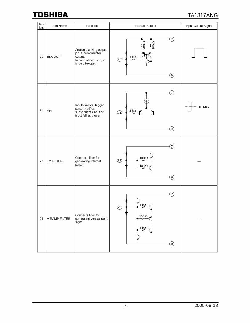
Pin No. Pin Name Function Interface Circuit Input/Output Signal
20 BLK OUT
Analog blanking output pin. Open collector output. In case of not used, it should be open.
21 VIN
Inputs vertical trigger pulse. Notifies subsequent circuit of input fall as trigger.
22 TC FILTER Connects filter for generating internal pulse.
⎯
23 V-RAMP FILTER Connects filter for generating vertical ramp signal.
⎯
200
Ω
20
9
7
1 kΩ
200
Ω
21
9
7
2 kΩ
22
9
7
100 Ω
10 kΩ
Th: 1.5 V
23
9
7
1 kΩ
100 Ω
1 kΩ
TA1317ANG
2005-08-18 8
Pin No. Pin Name Function Interface Circuit Input/Output Signal
24 AGC FILTER
Connects filter used to automatically adjust oscillation amplitude of vertical ramp signal. Can switch AGC sensitivity by BUS write function.
⎯
3.2
V
24
9
7
1 kΩ
2.25
V 50
0 Ω
500
Ω
TA1317ANG
2005-08-18 9
Bus Control Map
Write Mode Slave Address: 8CH (10001100)
Sub-Address D7 MSB
D6
D5
D4
D3
D2
D1
D0 LSB
Preset MSB LSB
00 PICTURE HEIGHT VD 1000 0000
01 PICTURE WIDTH1 V SHIFT 1000 0000
02 V LINEARITY V-EHT COMPENSATION 1000 0000
03 ANALOG V-BLK STOP PHASE H-EHT COMPENSATION 1000 0000
04 ANALOG V-BLK START PHASE V-RAMP LIMIT2 1000 0000
05 V CENTERING V-RAMP LIMIT1 1000 0000
06 V-DF PHASE V-DF AMPLITUDE 1000 1000
07 H-DF PHASE H-DF AMPLITUDE 1000 1000
08 H-DF CURVE V INTEGRAL CORRECTION 1000 0000
09 V AGC V S CORRECTION 1000 0000
0A * * EW PARABOLA 1000 0000
0B EW TRAPEZIUM V STOP 1000 0000
0C EW TOP CORNER * * PICTURE WIDTH2 1000 0000
0D EW BOTTOM CORNER * * * 1000 0000
0E EW S CORRECTION * * * 1000 0000
0F EW CORNER * * * 1000 0000
10 CENTER PARABOLA CENTER SAW 1000 1000
11 V SYMMETRY 0000 0000
Read Mode
Slave Address: 8DH (10001101)
D7 MSB
D6
D5
D4
D3
D2
D1
D0 LSB
0 V DF H DF LVP V NF V GUARD EW OUT V OUT POR
TA1317ANG
2005-08-18 10
Bus Control Function
Write Mode
Register Name/Number of Bits Function Explanation Output Change Picture Change Preset
PICTURE HEIGHT/7 Adjusts the picture height.
0000000: min 1000000: center 1111111: max
center
(1000000)
VD/1 Changes V-DRIVE mode
0: DC-coupling 1: AC-coupling ⎯ ⎯
DC-coupling
(0)
PICTURE WIDTH/7 Adjusts the picture width.
0000000: max 1000000: center 1111111: min
Sub-address 0C-D0 bit comes LSB.
center
(1000000)
V SHIFT/2 Where VD = 0, sets DAC output level of pin 2 is set. Where VD = 1, sets DC level of V-DRIVE is adjusted.
00: min
11: max
min
(00)
V LINEARITY/5 Corrects the vertical linearity.
00000: min 10000: center 11111: max
center
(10000)
Pin 6
Pin 6 (VD = 1)
Pin 6
Pin 11
Solid line Dashed line
Solid line Dashed line
VD = 1
Solid line Dashed line
Solid line Dashed line
TA1317ANG
2005-08-18 11
Register Name/Number of Bits Function Explanation Output Change Picture Change Preset
V-EHT COMPENSATION/3 Adjusts the compensated rate for the V-DRIVE by EHT-IN (pin 3).
000: min 111: max
min
(000)
ANALOG V-BLK STOP PHASE/5 Sets the analog blanking stop phase on pin 20. Inputs the output from pin 20 to an external BLK-IN of synchronization IC.
00000: min 10000: center 11111: max ⎯
center
(10000)
H-EHT COMPENSATION/3 Adjusts the compensated rate for the EW output by EHT-IN (pin 3).
000: min 111: max
min
(000)
ANALOG V-BLK START PHASE/5 Sets the analog blanking start phase on pin 20. Inputs the output from pin 20 to external BLK-IN of synchronization IC.
00000: min 10000: center 11111: max ⎯
center
(10000)
V-RAMP LIMIT LEVEL/4 Sets the V-ramp slice level.
0000: OFF 0001: min 1111: max
Sub-address 05-D0 bit comes MSB.
⎯ OFF
(0000)
Pin 6
Solid line Dashed line
Solid line Dashed line
Solid line Dashed line
Pin 6
Solid line Dashed line
Pin 11
TA1317ANG
2005-08-18 12
Register Name/Number of Bits Function Explanation Output Change Picture Change Preset
V CENTERING/7 Where VD = 0, DC level of V-DRIVE is adjusted. Where VD = 1, DAC output level of pin 2 is set.
0000000: min
1000000: center
1111111: max
min
(0000000)
V-DF PHASE/4 Adjusts the phase of the vertical dynamic focus output.
0000: min 1000: center 1111: max
⎯ center
(1000)
V-DF AMPLITUDE/4 Adjusts the amplitude of the vertical dynamic focus output.
0000: min 1000: center 1111: max
⎯ center
(1000)
H-DF PHASE/4 Adjusts the phase of the horizontal dynamic focus output.
0000: min 1000: center 1111: max
⎯ center
(1000)
Pin 18
Pin 6 (VD = 0)
Solid line Dashed line
VD = 0
Pin 16
Pin 18
TA1317ANG
2005-08-18 13
Register Name/Number of Bits Function Explanation Output Change Picture Change Preset
H-DF AMPLITUDE/4 Adjusts the amplitude of the horizontal dynamic focus output.
0000: min 1000: center 1111: max
⎯ center
(1000)
H-DF CURVE/4 Adjusts the curve characteristic of the horizontal dynamic focus output.
0000: max 1111: min
⎯ max
(0000)
V INTEGRAL CORRECTION/4 Adjusts the vertical integral correction.
0000: min 1111: max
min
(0000)
V AGC/2 Sets the AGC gain for V-ramp.
00: LOW 11: HIGH ⎯ ⎯
LOW
(00)
V S CORRECTION/6 Adjusts the vertical S correction.
000000: min 100000: center 111111: max
min
(000000)
EW PARABOLA/6 Adjusts the amplitude of the EW output.
000000: min 111111: max
min
(000000)
Pin 16
Pin 6
Pin 11
Solid line Dashed line
Solid line Dashed line
Pin 16
Solid line Dashed line
Pin 6
TA1317ANG
2005-08-18 14
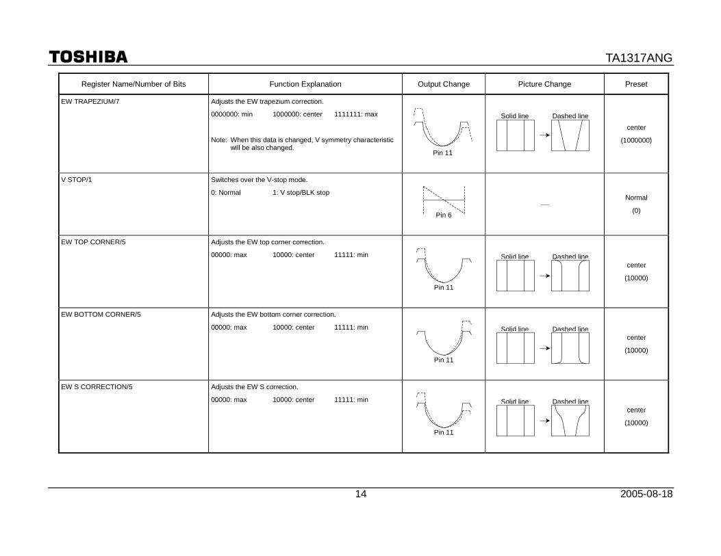
Register Name/Number of Bits Function Explanation Output Change Picture Change Preset
EW TRAPEZIUM/7 Adjusts the EW trapezium correction.
0000000: min 1000000: center 1111111: max
Note: When this data is changed, V symmetry characteristic will be also changed.
center
(1000000)
V STOP/1 Switches over the V-stop mode.
0: Normal 1: V stop/BLK stop
⎯ Normal
(0)
EW TOP CORNER/5 Adjusts the EW top corner correction.
00000: max 10000: center 11111: min
center
(10000)
EW BOTTOM CORNER/5 Adjusts the EW bottom corner correction.
00000: max 10000: center 11111: min
center
(10000)
EW S CORRECTION/5 Adjusts the EW S correction.
00000: max 10000: center 11111: min
center
(10000)
Pin 6
Pin 11
Solid line Dashed line
Solid line Dashed line
Pin 11
Pin 11
Solid line Dashed line
Solid line Dashed line
Pin 11
TA1317ANG
2005-08-18 15
Register Name/Number of Bits Function Explanation Output Change Picture Change Preset
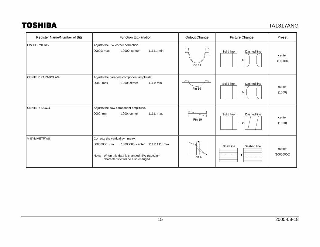
EW CORNER/5 Adjusts the EW corner correction.
00000: max 10000: center 11111: min
center
(10000)
CENTER PARABOLA/4 Adjusts the parabola-component amplitude.
0000: max 1000: center 1111: min
center
(1000)
CENTER SAW/4 Adjusts the saw-component amplitude.
0000: min 1000: center 1111: max
center
(1000)
V SYMMETRY/8 Corrects the vertical symmetry.
00000000: min 10000000: center 11111111: max
Note: When this data is changed, EW trapezium characteristic will be also changed.
center
(10000000)
Pin 11
Solid line Dashed line
Solid line Dashed line
Solid line Dashed line
Pin 19
Pin 19
Solid line Dashed line
Pin 6
TA1317ANG
2005-08-18 16
Read Mode
Register Name/Number of Bits Function Explanation
V DF/1 Vertical dynamic focus output self-check.
0: NG (no) 1: OK (yes)
H DF/1 Horizontal dynamic focus output self-check.
0: NG (no) 1: OK (yes)
LVP/1 LVP (low voltage protection) is detected.
0: OFF (pin 17 is high) 1: ON (pin 17 is low)
V NF/1 V-NF input self-check.
0: NG (no) 1: OK (yes)
V GUARD/1 Detects abnormality on V-NF input. If abnormal, Pin 20 goes high.
0: OFF (normal) 1: ON (abnormal)
EW OUT/1 EW output self-check.
0: NG (no) 1: OK (yes)
V OUT/1 V-DRIVE output self-check.
0: NG (no) 1: OK (yes)
POR/1 Power-on reset. Responds with 0 at first reading after power-on, 1 at second reading.
0: Resister preset 1: Normal
TA1317ANG
2005-08-18 17
Data Transfer Formats via I2C Bus
Slave address
A6 A5 A4 A3 A2 A1 A0 W/R
1 0 0 0 1 1 0 0/1
Start and Stop Condition
Bit Transfer
Acknowledge
SDA
SCL
S
Start condition
P
Stop condition
SDA
SCL
SDA stable Change of SDA allowed
SDA by transmitter
Only bit 9: Low impedance
Clock pulse for acknowledge S
1 8 9
SDA by receiver
SCL from master
Bit 9: High impedance
TA1317ANG
2005-08-18 18
Data Transmit Format 1
Data Transmit Format 2
Data Receive Format
At the moment of the first acknowledge, the master transmitter becomes a receiver and the slave receiver
becomes a transmitter. The Stop condition is generated by the master.
Optional Data Transmit Format: Automatic Increment Mode
In this transmission method, sub-addresses are incremented automatically and data is set from the specified
sub-address.
I2C BUS Conditions
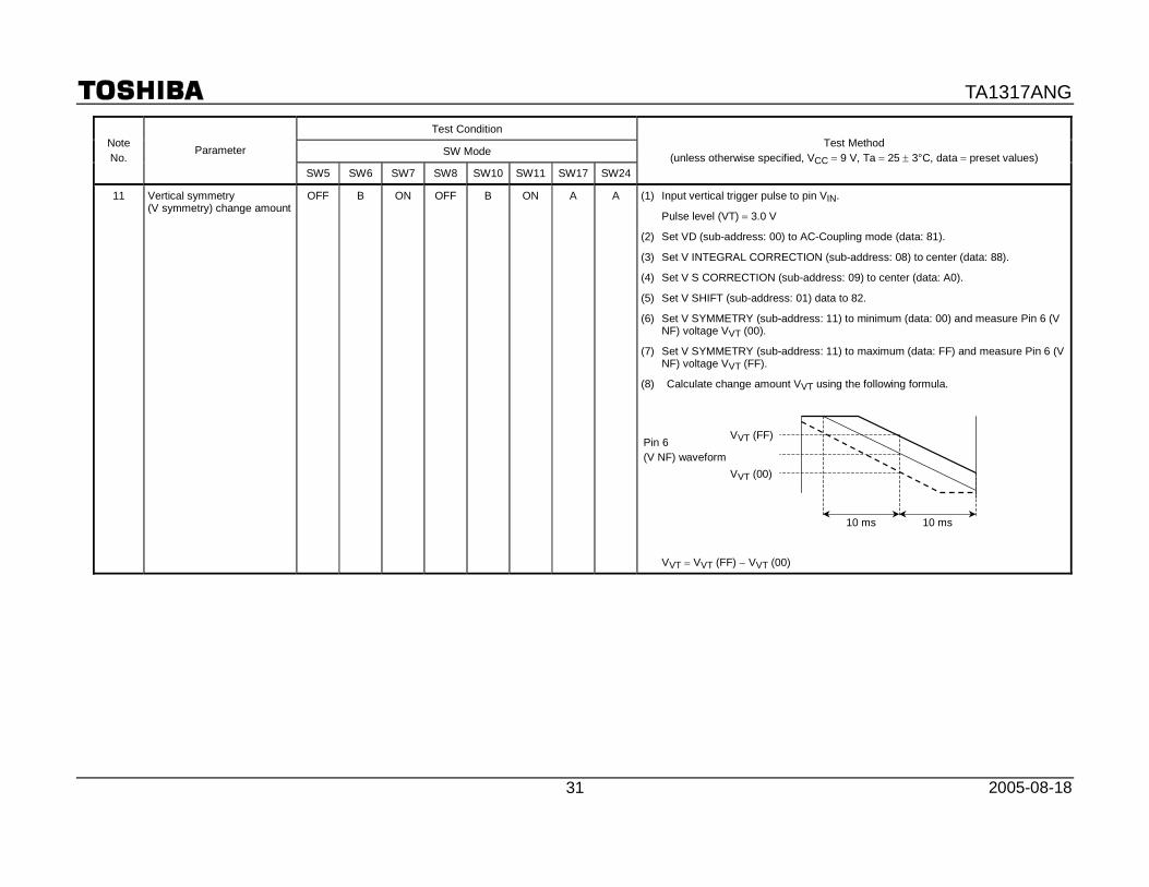
Characteristics Symbol Min Typ. Max Unit
Low level input voltage VIL 0 ⎯ 1.5 V
High level input voltage VIH 2.7 ⎯ Vcc V
Low level output voltage at 3 mA sink current VOL1 0 ⎯ 0.4 V
Input current each I/O pin with an input voltage between 0.1 VDD and 0.9 VDD Ii −10 ⎯ 10 µA
Capacitance for each I/O pin Ci ⎯ ⎯ 10 pF
SCL clock frequency fSCL 0 ⎯ 100 kHz
Hold time START condition tHD;STA 4.0 ⎯ ⎯ µs
Low period of SCL clock tLOW 4.7 ⎯ ⎯ µs
High period of SCL clock tHIGH 4.0 ⎯ ⎯ µs
Set-up time for a repeated START condition tSU;STA 4.7 ⎯ ⎯ µs
Data hold time tHD;DAT 100 ⎯ ⎯ ns
Data set-up time tSU;DAT 250 ⎯ ⎯ ns
Set-up time for STOP condition tSU;STO 4.0 ⎯ ⎯ µs
Bus free time between a STOP and START condition tBUF 4.7 ⎯ ⎯ µs
S Slave address 0 A Transmit data ASub address A P7 bit
MSB S: Start condition
8 bit
MSB A: Acknowledge
9 bit
MSBP: Stop condition
S Slave address 0 A Transmit data ASub address A
Transmit data nASub address A P
・・・・・・
・・・・・・
S Slave address 1 A AReceive data P7 bit
MSB
8 bit
MSB
S Slave address A Transmit data 2 ・・・・Transmit data 1 A P 7 bit
MSB
8 bit
MSB
0 Sub address 7 bit
MSB
A 1 8 bit
MSB
TA1317ANG
2005-08-18 19
Maximum Ratings (Ta = 25°C)
Characteristics Symbol Rating Unit
Power supply voltage VCCmax 12 V
Input pin voltage Vin GND − 0.3 to VCC + 0.3 V
Power dissipation PD (*) 1250 mW
Power dissipation reduction rate 1/θja −10 mW/°C
Operating temperature Topr −20~65 °C
Storage temperature Tstg −55~150 °C
*: See the figure below.
Operating Conditions
Characteristics Description Min Typ. Max Unit
Supply voltage (VCC) Pin 7 8.5 9.0 9.5 V
EHT input voltage Pin 3 0.0 ⎯ 9.0 V
FBP input amplitude Pin 12 4.0 ⎯ 9.0 V
FBP input frequency Pin 12 28 ⎯ 45 kHz
FBP input width Pin 12 2.5 ⎯ ⎯ µs
SCL/SDA pull-up voltage Pins 13 & 14 3.0 5.0 9.0 V