IEEE TRANSACTIONS ON NUCLEAR SCIENCE, VOL. 50, NO. 3, JUNE 2003 483
Total Ionizing Dose Effects in MOS Oxides andDevices
T. R. Oldham, Fellow, IEEE,and F. B. McLean, Fellow, IEEE
Abstract—This paper reviews the basic physical mechanisms ofthe interactions of ionizing radiation with MOS oxides, includingcharge generation, transport, trapping and detrapping, and inter-face trap formation. Device and circuit effects are also discussedbriefly.
Index Terms—CMOS, ionizing radiation, microelectronics,MOS, radiation effects.
I. INTRODUCTION
T HE DEVELOPMENT of military and space electronicstechnology has traditionally been heavily influenced by
the commercial semiconductor industry. The development ofMOS technology, and particularly CMOS technology, as dom-inant commercial technologies has occurred entirely within thelifetime of the NSREC. For this reason, it is not surprising thatthe study of radiation interactions with MOS materials, devices,and circuits has been a major theme of this conference for mostof its history.
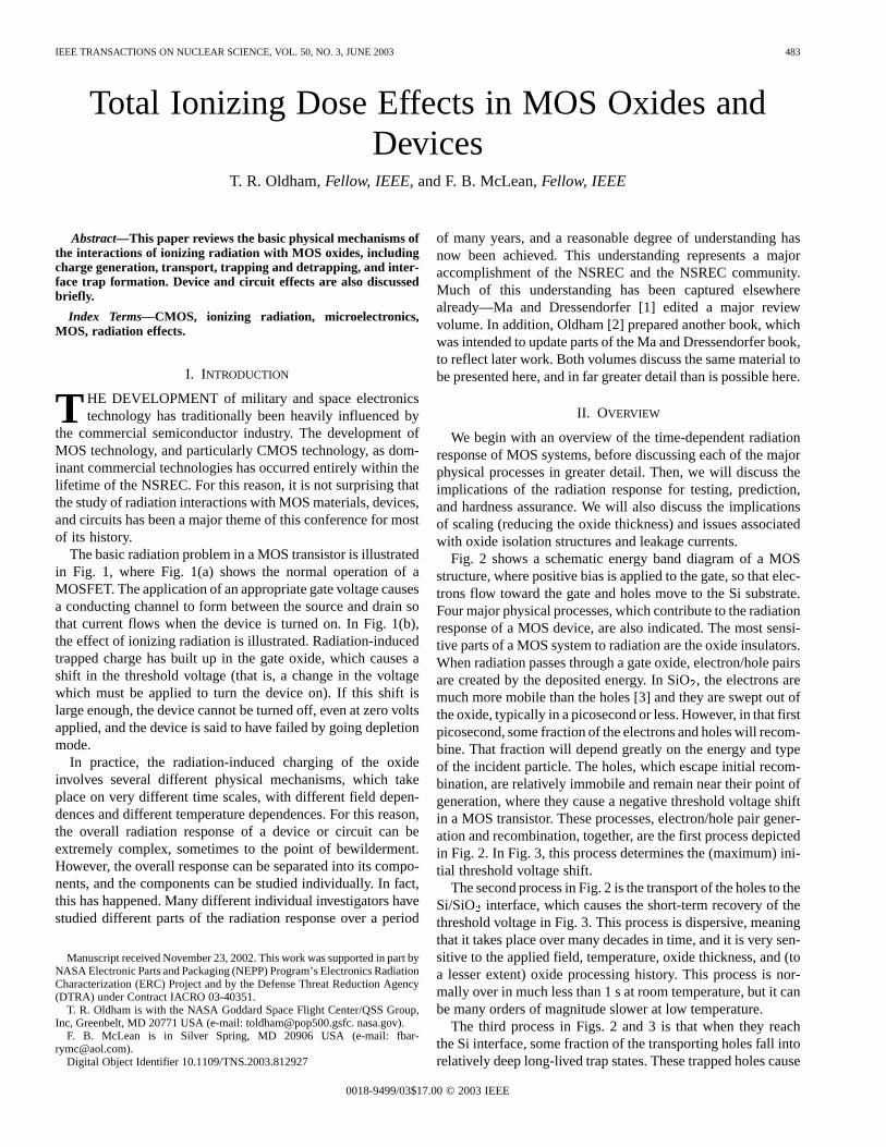
The basic radiation problem in a MOS transistor is illustratedin Fig. 1, where Fig. 1(a) shows the normal operation of aMOSFET. The application of an appropriate gate voltage causesa conducting channel to form between the source and drain sothat current flows when the device is turned on. In Fig. 1(b),the effect of ionizing radiation is illustrated. Radiation-inducedtrapped charge has built up in the gate oxide, which causes ashift in the threshold voltage (that is, a change in the voltagewhich must be applied to turn the device on). If this shift islarge enough, the device cannot be turned off, even at zero voltsapplied, and the device is said to have failed by going depletionmode.
In practice, the radiation-induced charging of the oxideinvolves several different physical mechanisms, which takeplace on very different time scales, with different field depen-dences and different temperature dependences. For this reason,the overall radiation response of a device or circuit can beextremely complex, sometimes to the point of bewilderment.However, the overall response can be separated into its compo-nents, and the components can be studied individually. In fact,this has happened. Many different individual investigators havestudied different parts of the radiation response over a period
Manuscript received November 23, 2002. This work was supported in part byNASA Electronic Parts and Packaging (NEPP) Program’s Electronics RadiationCharacterization (ERC) Project and by the Defense Threat Reduction Agency(DTRA) under Contract IACRO 03-40351.
T. R. Oldham is with the NASA Goddard Space Flight Center/QSS Group,Inc, Greenbelt, MD 20771 USA (e-mail: [email protected]. nasa.gov).
F. B. McLean is in Silver Spring, MD 20906 USA (e-mail: [email protected]).
Digital Object Identifier 10.1109/TNS.2003.812927
of many years, and a reasonable degree of understanding hasnow been achieved. This understanding represents a majoraccomplishment of the NSREC and the NSREC community.Much of this understanding has been captured elsewherealready—Ma and Dressendorfer [1] edited a major reviewvolume. In addition, Oldham [2] prepared another book, whichwas intended to update parts of the Ma and Dressendorfer book,to reflect later work. Both volumes discuss the same material tobe presented here, and in far greater detail than is possible here.
II. OVERVIEW
We begin with an overview of the time-dependent radiationresponse of MOS systems, before discussing each of the majorphysical processes in greater detail. Then, we will discuss theimplications of the radiation response for testing, prediction,and hardness assurance. We will also discuss the implicationsof scaling (reducing the oxide thickness) and issues associatedwith oxide isolation structures and leakage currents.
Fig. 2 shows a schematic energy band diagram of a MOSstructure, where positive bias is applied to the gate, so that elec-trons flow toward the gate and holes move to the Si substrate.Four major physical processes, which contribute to the radiationresponse of a MOS device, are also indicated. The most sensi-tive parts of a MOS system to radiation are the oxide insulators.When radiation passes through a gate oxide, electron/hole pairsare created by the deposited energy. In SiO, the electrons aremuch more mobile than the holes [3] and they are swept out ofthe oxide, typically in a picosecond or less. However, in that firstpicosecond, some fraction of the electrons and holes will recom-bine. That fraction will depend greatly on the energy and typeof the incident particle. The holes, which escape initial recom-bination, are relatively immobile and remain near their point ofgeneration, where they cause a negative threshold voltage shiftin a MOS transistor. These processes, electron/hole pair gener-ation and recombination, together, are the first process depictedin Fig. 2. In Fig. 3, this process determines the (maximum) ini-tial threshold voltage shift.
The second process in Fig. 2 is the transport of the holes to theSi/SiO interface, which causes the short-term recovery of thethreshold voltage in Fig. 3. This process is dispersive, meaningthat it takes place over many decades in time, and it is very sen-sitive to the applied field, temperature, oxide thickness, and (toa lesser extent) oxide processing history. This process is nor-mally over in much less than 1 s at room temperature, but it canbe many orders of magnitude slower at low temperature.
The third process in Figs. 2 and 3 is that when they reachthe Si interface, some fraction of the transporting holes fall intorelatively deep long-lived trap states. These trapped holes cause
484 IEEE TRANSACTIONS ON NUCLEAR SCIENCE, VOL. 50, NO. 3, JUNE 2003
Fig. 1. Schematic of n-channel MOSFET illustrating radiation-induced charging of the gate oxide: (a) normal operation and (b) post-irradiation.
Fig. 2. Schematic energy band diagram for MOS structure, indicating majorphysical processes underlying radiation response.
a remnant negative voltage shift, which can persist for hours oreven for years. But even these stable trapped holes undergo agradual annealing, which is illustrated in Fig. 3.
The fourth major component of MOS radiation responseis the radiation-induced buildup of interface traps right at theSi/SiO interface. These traps are localized states with energylevels in the Si band-gap. Their occupancy is determined bythe Fermi level (or by the applied voltage), giving rise to avoltage-dependent threshold shift. Interface traps are highlydependent on oxide processing and other variables (appliedfield and temperature).
Fig. 3 is schematic in that it does not show real data, butit reasonably represents the main features of the radiation re-sponse of a hardened n-channel MOS transistor. The range ofdata, from 10 s to 10 s, is enormous, as it has to be to in-clude qualitatively the four main processes we have discussed.For the oxide illustrated in Fig. 3, a relatively small fraction ofthe holes reaching the interface are trapped, which is why wesay it is realistic for a hardened oxide. Many oxides would trapmore charge than is shown here. In addition, the final thresholdshift, including interface traps, is positive (the so-called reboundor superrecovery effect) here because the number of negativelycharged interface traps finally exceeds the number of trappedholes. Not all oxides really have this behavior, but it is one ofthe results which can be considered “typical.”
Fig. 3. Schematic time-dependent post-irradiation threshold voltage recoveryof n-channel MOSFET, relating major features of the response to underlyingphysical processes.
III. D ESCRIPTION OFBASIC PHYSICAL PROCESSES
UNDERLYING THE RADIATION RESPONSE OFMOS DEVICES
Next, we consider these basic physical mechanisms in moredetail and provide critical references. But for a complete review,the readers should consult the references.
A. Electron-Hole Pair Generation Energy
The electron/hole pair creation energy was determined tobe 18 3 eV by Ausman and McLean [4], based on experimentaldata obtained by Curtiset al.[5]. This result has been confirmedindependently by others [6], [7], including a more accurate setof measurements and analysis by Benedetto and Boesch, Jr. [8],which established eV. From this value of , onecan calculate the charge pair volume density per rad,
pairs cm -rad. But this initial density is quickly reducedby the initial recombination process, which we discuss next.
B. Initial Hole Yield
The electrons are swept out of the oxide very rapidly, in atime on the order of a picosecond, but in that time some frac-tion of them recombine with the holes. The fraction of holes es-caping recombination, , is determined mainly by two
OLDHAM AND M CLEAN: TOTAL IONIZING DOSE EFFECTS IN MOS OXIDES AND DEVICES 485
factors: the magnitude of the electric field, which acts to sepa-rate the pairs, and the initial line density of charge pairs createdby the incident radiation. The pair line density is determined bythe linear energy transfer (LET), and is, therefore, a function ofthe incident particle type and energy. The line density is also in-versely proportional to the average separation distance betweenelectron/hole pairs; obviously, the closer the average spacing ofthe pairs, the more recombination will occur at a given field, andthe less the final yield of holes will be.
The recombination problem cannot be solved analytically forarbitrary line density, but analytic solutions do exist for the lim-iting cases, where the pairs are either far apart or very closetogether. These cases are illustrated in Fig. 4. Fig. 4(a) showsthe so-called geminate recombination model, where the averageseparation between pairs is much greater than the thermalizationdistance, the distance between the hole and the electron. Onecan treat the interaction between the charges of an isolated pair,which have a mutual coulomb attraction, which undergo driftmotion in opposite directions under the influence of the appliedfield, and which have a random diffusion motion driven by thethermal fluctuations of the system. But interactions with otherpairs can be neglected. The geminate recombination model wasfirst formulated by Smoluchowski [9] and later solved by On-sager [10], originally for the recombination of electrons andpositive ions in gases. Experimental and theoretical results forthe geminate process are shown in Fig. 5, where the theoreticalcurve was obtained by Ausman [11], assuming the average ther-malization radius to be 5 nm.
The other case, called columnar recombination, is illustratedin Fig. 4(b), where the separation between pairs is much lessthan . There are several electrons closer to any given hole thanthe electron, which was its original partner, so the probability ofrecombination is obviously much greater than in the geminatecase. The columnar model was originally solved analytically byJaffe [12], extending earlier work by Langevin [13]. More re-
Fig. 5. Fractional yield as a function of applied field for Co60 gamma rays,12-MeV electrons, and geminate model calculations [7], [11], [17].
Fig. 6. Fractional yield as a function of applied field for alpha particlesincident on SiO. Solid lines indicate columnar model results for differentinitial column radii [14], [16].
cently, Oldham [14]–[16] has presented a more accurate numer-ical solution of the Jaffe equation, which extends the range ofapplicability of the model. Representative experimental data, for2 MeV alpha particles, are presented in Fig. 6 [14], along withtheoretical curves. The parameteris the half-diameter assumedfor the initial Gaussian charge distribution. Recombination re-sults for a variety of incident particles are summarized in Fig. 7[17]. At a field of 1 MV/cm, there is a difference of more thanan order of magnitude in the yields shown for different parti-cles. Clearly, recombination is an important effect, which mustbe accounted for, when comparing the effect of different radi-ation sources. One case of considerable practical importance isthe comparison of yield between Cogamma rays and 10 keV
486 IEEE TRANSACTIONS ON NUCLEAR SCIENCE, VOL. 50, NO. 3, JUNE 2003
Fig. 7. Experimentally measured fractional hole yield as a function of appliedfield, for a number of incident particles.
Fig. 8. Recombination measurements and calculations for protons incident onSiO .N andp refer to n- and p-channel transistors, respectively.
X-rays, which has been studied extensively by several differentgroups [8], [17]–[19].
As one might expect, there are also a number of intermediatecases of practical interest, where neither model is strictly appli-cable, as illustrated in Fig. 8. The original version of this figurewas published by Oldham [20] in 1984, based on experimentaldata by Stassinopouloset al. [21]–[23] and Bruckeret al. [24],[25]. But additional data points have been added from time-to-time, as other experiments were reported [26]–[28]. These laterexperiments have generally reported lower yield (that is, morerecombination) than the earlier experiments. The different ex-periments have all been done at different fields, so the gem-inate model limit is different in each case, which is not indi-cated in Fig. 8. Strictly speaking, the theoretical curves in Fig. 8apply only to the Stassinopoulos and Brucker measurements.The other key point is that the LET for a proton and an elec-tron is not really the same until their energy is about 1000 MeV,well above the energy of any incident particle in any of these ex-periments. In the original version of Fig. 8, the geminate modelwas indicated schematically to apply from 1000 MeV down toabout 150 MeV because it appeared to fit the data available atthat time. But the more recent data indicates that the recombi-
nation process is not purely geminate until the proton energy iswell above 100–200 MeV.
C. Hole Transport
The transport of holes through the oxide layer has beenstudied extensively by several groups [29]–[40], and it hasthe following properties: 1) Transport is highly dispersive,taking place over many decades in time following a radiationpulse. 2) It is universal in nature, meaning that changes intemperature, field, and thickness do not change the shape ordispersion of the recovery curves on a log-time plot. Changesin these variables affect only the time-scale of the recovery.3) The transport is field activated. 4) At temperatures aboveabout 140 K, the transport is strongly temperature activated,but it is not temperature activated below about 140 K. 5) Thehole transport time, or recovery time, has a strong super-linearpower law dependence on oxide thickness.
The best overall description of the experimental holetransport data seems to be provided by the contin-uous-time-random-walk (CTRW) hopping transport formalism,which was originally developed by Montroll and others[41]–[44]. This formalism has been applied to hole transportin silicon dioxide by McLean [29], [32], [33], [37]–[40] andby Hughes [30], [31], [36]. (However, the multiple trappingmodel [34], [35] also accounts for many of the features ofthe experimental data.) The specific transfer mechanismseems most likely to be small polaron hopping of the holesbetween localized shallow trap states having a random spatialdistribution, but having an average separation of about 1 nm.The term polaron refers to the situation where the carrierinteracts strongly with the surrounding medium, creating alattice distortion in its immediate vicinity (also referred to asself-trapping). As the hole hops through the material, it carriesthe lattice distortion with it. The strongest evidence for thepolaron hopping mechanism is the transition from thermallyactivated transport above about 140 k to nonactivated transportat lower temperatures. This transition is a classic signature ofpolaron hopping [44]–[47]. Many other features of the holetransport, such as dispersion, universality, and superlinearthickness dependence, can be attributed to a wide distributionof hopping times for the individual holes.
Representative experimental data are presented in Figs. 9–12.Fig. 9 shows the effect of temperature variation, and Fig. 10shows the effect of varying the electric field. In both figures,the results cover seven decades in log-time, following a shortradiation pulse. In both Figs. 9 and 10, the flatband voltage shiftis plotted as a function of log-time, normalized to the calculatedshift before any transport occurs. In Fig. 9, the field is 1 MV/cm,and the strong temperature activation above 140 K is apparent. InFig. 10, all the curves are taken at K. The universalityanddispersion of the transport is better illustrated in Fig. 11, whereall the curves from Fig. 9 are replotted for scaled time. The entiretransport process covers 14 decades in time (!), and all the curveshave the same “S” shape. The time, , at which the flat-bandvoltage reaches 50% recovery, has been used as the scalingparameter. The solid line is an analytical fit of the CTRW model,where the shape parameterhas the value 0.25. Finally, Fig. 12shows how the hole transit time varies with oxide thickness,
OLDHAM AND M CLEAN: TOTAL IONIZING DOSE EFFECTS IN MOS OXIDES AND DEVICES 487
Fig. 9. Normalized flatband voltage recovery following pulsed Linac 12-MeV electron irradiation of 96.5 nm oxide at different temperatures.
Fig. 10. Normalized flatband recovery data of Fig. 9 replotted with time scaledto half recovery time, showing universal response with respect to temperature(E = 1 MV/cm). Solid curve is CTRW model result for� = 0:25.
Fig. 11. Normalized flatband voltage recovery data following pulsed Linacelectron beam exposure of 96.5 nm oxide capacitor at 80 K for different fields.
as , or about . This oxide thickness dependence arisesbecause the farther the holes transport, the greater the probability
Fig. 12. Recovery time as a function of oxide thickness for etched-back andas-grown oxides.
that some of them will be in states where the next hop is a difficultone, one that takes a long time to happen. Then, the farther theholes go, the slower they move.
D. Deep Hole Trapping and Annealing
The most complete discussion of hole trapping and annealingis by Oldham [2]. Deep hole traps near the Si/SiOinterfacearise because there is a transition region where oxidation is notcomplete. This region contains excess Si, or oxygen vacancies,depending on how one looks at it. The oxidation process wasdescribed by Dealet al. [48] in an early review article, whichwas based on original work done even earlier. Eventually, Feigl
488 IEEE TRANSACTIONS ON NUCLEAR SCIENCE, VOL. 50, NO. 3, JUNE 2003
et al. [49] presented a convincing model for the single oxygenvacancy. Basically, there is one oxygen atom missing from theusual lattice configuration, leaving a weak Si–Si bond, whereeach Si atom is back-bonded to three oxygen atoms. When apositive charge is trapped, the Si–Si bond is broken, and the lat-tice relaxes. The key point that Feigl added to earlier discus-sions was that the relaxation is asymmetric-one atom relaxesinto a planar configuration, and the other remains in a tetra-hedral configuration. The oxygen vacancy was also eventuallyconnected to the center, originally detected by Weeks [50] in
-quartz, but also later detected in bulk glasses and thermallygrown SiO [51]. The correlation of centers, and oxygen va-cancies, with radiation-induced trapped holes was first estab-lished by Lenahan and Dressendorfer [51].
Oxide trapped holes are relatively stable, but they do undergo along-term annealing process which can extend for hours or evenyears, with a complex dependence on time, temperature, and ap-pliedfield.Generally,trappedholeannealingcanproceedbyeitherof twoprocesses, tunnelingor thermalexcitation.Atornear roomtemperature, tunnelingis thedominantmechanism,but if thetem-peratureisraisedenough,thethermalprocesswilleventuallydom-inate. Tunneling has been analyzed by several authors [52]–[58],as has the thermalprocess [59]–[71]. Both processescangive riseto the linear-with-log dependence thathasbeenobservedempir-ically [53]–[55], but one has to make different assumptions aboutthe trap energy level distribution for the two processes.
The study of radiation-induced trapped hole annealing hasled to new insights about the atomic structure of the oxide trap,which in turn has led to new insights into the structure of neutralelectron traps, which play a critical role in breakdown studiesand in other reliability problems. (For a full discussion, see [2].)One of the key results is illustrated in Fig. 13, originally re-ported by Schwanket al. [72]. An irradiated sample was an-nealed under positive bias at 100C for about one week, andall the trapped positive charge appeared to be removed. Butthen they applied a negative bias, and about half the neutral-ized positive charge was restored within a day. This result led tothe idea that annealing of radiation damage involved a compen-sation process. That is, defects were neutralized without beingremoved. Although other groups quickly confirmed the basicresult [57], [73], several years passed before Leliset al. did athorough study [74]–[76]. One of their key results is shown inFig. 14, where a hardened oxide is exposed to a short Linac radi-ation pulse and then subject to a series of alternating positive andnegative bias annealing steps. Under negative bias, a significantamount of neutralized positive charge reappears, but there isalso a significant amount of “true” annealing, where the trappedcharge really is removed. Leliset al. proposed a model, illus-trated in Fig. 15, to account for their results and results of others.Generally, it had been assumed that annealing was proceeded byan electron tunneling to the positively charged Si, neutralizing it,and reforming the Si–Si bond. Instead, Lelis proposed the elec-tron tunnels to the neutral Si, forming a dipole structure, wherethe extra electron can then tunnel back and forth to the substratein response to bias changes. This model is consistent with theelectron spin resonance (ESR) work of Lenahanet al. [51] andwith the electrical results of Schwank and others, explaining avariety of complex results in terms of a single defect, which was
Fig. 13. Trapped hole annealing; negative bias curve shows that “annealed”holes are not really removed [72].
already well known. The transition from Fig. 15(a) and (b) wasdescribed by Feiglet al.The transition from Fig. 15(b) and (c)and back describes the switching reported by Schwanket al.and by Leliset al. And the transition from Fig. 15(c) back toFig. 15(a) indicates the true annealing, which is also observed.
The dipole hypothesis by Leliset al.was attractive because itexplained many things very simply, but at first, it was also con-troversial. Itwascriticizedby threedifferentgroups [77]–[80] fordifferent reasons. The biggest problem was that putting an extraelectrononaneutralSiatominsteadofapositiveSi requiredover-cominganelectron–electronrepulsion.Lelisetal.pointedoutthataddingtheextraelectrontothepositiveSiwouldrequirechanginga planar configuration of atoms into a tetrahedral configuration,moving around atoms in the lattice to change bond angles, whichwould require adding energy. The energy to rearrange the latticemight be greater than the electron–electron energy, which wouldmeanstabledipoleswouldbeenergetically favored.But, initially,they lacked the means to quantify this argument, so debate con-tinued for several years.
Several other independent experiments produced results,which seemed to support the dipole hypothesis. These includedthermally stimulated current (TSC) measurements, first byShanfieldet al. [62]–[64], and later by Fleetwood [65]–[69]. Inaddition, Walterset al. [81] concluded that the dipole proposedby Lelis et al. acted as a neutral electron trap in their injectionexperiments. This work was an important independent confir-mation of the dipole hypothesis, but it was also a significantextension of it. Basically, they argued that the positive end ofthe dipole acted as an electron trap, so that a second electroncould be trapped, making the whole complex net negative. Thereason this result was important was that there is an enormousbody of literature on neutral electron traps and the critical rolethey play in nonradiation-induced reliability problems. (Thisliterature is too extensive to discuss here; see [2].) The Lelisetal. dipole hypothesis became an important piece of the puzzlefor explaining all this other work. And, finally, Conleyet al.[82], [83] conducted ESR experiments, where they cycledcharge back and forth by alternating bias, while monitoringthe signal. Their main result is shown in Fig. 16. Thedipole model was the only one consistent with this result, so itsettled the debate, at least on the experimental side. Even morerecently, two theoretical groups have done quantum mechanicalcalculations, using different mathematical approaches, whichhave also indicated that dipoles should be energetically favored
OLDHAM AND M CLEAN: TOTAL IONIZING DOSE EFFECTS IN MOS OXIDES AND DEVICES 489
Fig. 14. Alternate positive and negative bias annealing for capacitor exposed to 4-�s Linac pulse.
Fig. 15. Model of hole trapping, permanent annealing, and compensation processes.
under certain conditions [84], [85]. In addition, Fleetwoodet al.have recently extended this model to argue that it also accountsfor noise results, which they reported [86].
We note that, in recent years, there has been much discussionof the role of border traps, oxide traps that exchange charge withthe Si substrate. The proposal to call these traps border trapswas made by Fleetwood [87] in 1992. At that time, the dipolemodel by Leliset al.had been in the literature for four years andwas already well known. Now, more than ten additional yearshave passed, and the defect described by Leliset al. is still theonly confirmed border trap, at least in the Si/SiOsystem. Otherborder trap structures have occasionally been proposed [88], butthey have not done well in experimental tests [82], [83].
E. Radiation-Induced Interface Traps
Radiation-induced interface states have been identified withthe so-called resonance in ESR studies, by Lenahan andDressendorfer [89]. This center is a trivalent Si atom, back
Fig. 16. E density during alternate positive and negative bias annealing.
bonded to three other Si atoms, with a dangling bond extendinginto the oxide. This defect is amphoteric, negatively chargedabove mid-gap, neutral near mid-gap, and positively chargedbelow mid-gap. Lenahan and Dressendorfer showed a very
490 IEEE TRANSACTIONS ON NUCLEAR SCIENCE, VOL. 50, NO. 3, JUNE 2003
strong correlation between the buildup of the resonance andthe buildup of interface traps, as determined by electrical mea-surements. There is also an extensive literature suggesting thatthis same defect is also present as a process-induced interfacetrap. We cannot review all this literature here, but other reviewshave already been published [1], [2]. [90], [91]. (In particular,see [2, Ch. 3, refs.].) The basic picture, however, is that whenthe oxide is grown, there are still about 10cm unpassivatedtrivalent Si centers. In subsequent processing, almost all thesecenters are passivated by reacting with hydrogen. However,they can also be depassivated, either by radiation interactionsor by other environmental stresses.
Therehavebeenmanyconflictingmodelsproposedtodescribethe process(es) by which radiation produces interface traps, andmuch controversy about them. However, a reasonable degreeof consensus has finally emerged. All the models are consistentwith the idea that the precursor of the radiation-induced interfacetrap is a Si atom bonded to three other Si atoms and a hydrogenatom. When the Si–H bond is broken, the Si is left with anunpassivated dangling bond, as an electrically active defect.The process by which the Si atom is depassivated is where themodels differ.Now, it hasbecomeclear that the dominant processis a two-stage process involving hopping transport of protons,originally described by McLean [92], which was based on aseries of experimental studies by his coworkers [93]–[101]. Thiswork wasconfirmedandextended ina seriesof additional studiesby Saks and his coworkers [102]–[108]. In the first stage of thisprocess, radiation-induced holes transport through the oxide,and free hydrogen, in the form of protons. In the second stage,the protons undergo hopping transport (following the CTRWformalism described above). When the protons reach the inter-face, they react, breaking the SiH bonds already there, formingH and a trivalent Si defect. One of the critical experimentalresults is shown in Fig. 17 [90], [101], which shows the resultsof bias switching experiments. For curve A, the sample wasirradiated under positive bias, which was maintained throughoutthe experiment, and a large interface trap density eventuallyresulted. For curve B, the bias was negative during irradiationand hole transport, so the holes were pushed away from theinterface, but the bias was switched positive after 1 s, duringthe proton transport. The final number of interface states forcurves A and B is almost the same, however. For curve E, thebias is maintained negative throughout both stages, and interfacetrap production is suppressed completely. For curves C and D,the bias is negative during irradiation and hole transport butswitched positive later than for curve B. In all cases, bias polarityduring the hole generation and transport made no difference,but positive bias during the proton transport was necessary tomove the protons to the Si/SiOinterface. The time scale of theinterface trap buildup was determined by the transport time ofthe protons. (For curves B, C, and D, the protons were initiallypushed away from the interface, so it took them longer to getthere after the proper bias was applied.) McLean also worked outthe average hopping distance for protons to be 0.26 nm, which isthe average distance between oxygen atoms. And, he determinedthe activation energy for the interface trap buildup to be 0.82 eV,which is consistent with proton transport [109]. Saks eventuallysucceeded in monitoring the motion of the protons directly [106].
Fig. 17. Experimental results from field switching experiments that supportH+ transport model.
Fig. 18. Isochronal annealing results showing small neutral hydrogendiffusion process and larger H+ transport process for interface trap formation[103].
The two-stage proton transport model is a robust model atthis point. It has been confirmed by different groups (McLeanand coworkers, and Saks and coworkers), using different teststructures (capacitors and transistors, respectively), differentgate technologies (Al active metal and poly-Si, respectively),and different measurement techniques (C–V analysis andcharge pumping respectively). Despite all these variations,this process has always been the main effect. However, it doesnot explain everything. Boesch, Jr. [110] and Saks [103] haveidentified a second-order effect, where a small part of theinterface trap buildup seems to correlate with the arrival oftransporting holes at the interface. Presumably, the holes breakthe Si–H bonds instead of protons. Also, Griscom [111] andBrown [112] had proposed originally that diffusion of neutralhydrogen, rather than drift transport of protons, was the mainmechanism for interface trap production. But, Sakset al. [103]were able to isolate the neutral hydrogen effect and showedthat it was also small. The key result is shown in Fig. 18, wherethe interface trap buildup between 120 and 150 K is due toneutral hydrogen, and the buildup above 200 K is due to protontransport. The vertical scale is a log scale here, so the neutralhydrogen process accounts for only a few percent of the totalbuild-up. Griscom and Brown both eventually endorsed theMcLean model [113].
OLDHAM AND M CLEAN: TOTAL IONIZING DOSE EFFECTS IN MOS OXIDES AND DEVICES 491
There have also been several models proposed where trappedholes are somehow converted to interface traps—usually thedetails of the conversion process are not specified [114]–[118].Thesemodelsarenotwell regardedtoday.Forexample, inFig.17,curves B and E have the same hole trapping. For this reason,one might expect these models to predict similar interface trapbuildups, contrary to what is shown in the figure. If one studieshole trap removal and interface trap buildup carefully, the twoprocesseshavedifferent timedependences,different temperaturedependences, and different bias dependences. They have thesame dose dependence, but otherwise seem to be completelyindependent. Here, we cannot discuss these things in detail, butfulldiscussionsappear in [2,Ch.3]and in [88].However,Oldhamet al.[90] provided a reasonable explanation for experimental re-sults purporting to show trapped hole conversions. They pointedout that trapped holes that donotundergo a defect transformationcan account for most of these results; that is, trapped holes looklike interface traps in some experiments. (The model for theseholes is discussed in Section III-D.) The exchange of chargebetween trapped holes and the Si substrate has been extensivelystudied since then (usually under the name border traps) [88],[119], and the idea that such charge exchange takes place is nolonger considered unusual.
Finally, some samples exhibit what has been called a latent in-terface trap buildup, which is illustrated in Fig. 19 [120]. This ef-fect is thought to be due to hydrogen diffusing into the gate oxideregion from another part of the structure, perhaps the field oxideor an encapsulating layer. The latency period arises because thehydrogen is diffusing from (relatively) far away. From a testingpoint of view, this is a difficult effect to account for. There is notrace of it on the time scale of most laboratory tests, yet it caneventually be a large, even dominant, effect, on a time scale ofmonths. Sakset al. [108] subsequently reported that the latentbuildup is suppressed by a nitride encapsulating layer, whichserves as a barrier to hydrogen diffusion. Unless one knows howthe samples are encapsulated, it is not possible to predict aheadof time whether a latent buildup will occur or not.
IV. I MPLICATIONS FOR RADIATION TESTING,HARDNESSASSURANCE, AND PREDICTION
We have now completed our review of the basic physicalmechanisms underlying the radiation response of CMOS de-
Fig. 20. V , V , andV annealing; long term response illustrates reboundeffect [72].
vices. Next, we consider these mechanisms in the context ofdevice and circuit testing, hardness assurance, and prediction.
A. Rebound or Super-Recovery
The rebound effect is illustrated in Fig. 20 [72] whichshows threshold voltage shift for a MOSFET, alongwith its components, oxide trapped charge andinterface trapped charge , during both irradiation andpost-irradiation annealing. The annealing data is shown for twotemperatures, 25C and 125 C.
After irradiation, the threshold shift is less than 1 V, but thisrelatively small shift is obtained by compensating positive oxidetrapped charge with negatively charged interface traps (in thisn-channel device). When the hole traps anneal, however, thefinal threshold shift is positive, about 3.5 V, which is more thanenough to fail the device. The effect of raising the temperature isto anneal the hole traps faster, but the same final state is reachedat room temperature. One could imagine a device that faileddue to trapped positive charge immediately after irradiation, thatwould later work properly for a time as some of the holes an-nealed, that would then fail again later from trapped negativecharge as more of the holes annealed. There is very little changein interface trap density during the annealing process at eithertemperature, so the late time failure would be due to interfacetraps that were there at the end of the irradiation.
To test for rebound, there is now a standard test method,1019.4, which calls for a 100C anneal for 168 hours, whichwill detect the effect in oxides similar to the one used in Fig. 20[121]. This method represents a compromise, because 100Cis not a high enough temperature to accelerate the trapped holeannealing in all oxides, but if one goes much higher in temper-ature, the interface traps may anneal too [89].
The rebound effect is of great practical concern for space en-vironments because components are typically exposed to rel-atively low dose rates for very long mission lifetimes. Thereis now strong emphasis on using unhardened commercial tech-nology as much as possible, which is reasonable to consider inspace because oxide traps may anneal as fast as they are created,or nearly so. A component that fails at a low dose in a laboratory
492 IEEE TRANSACTIONS ON NUCLEAR SCIENCE, VOL. 50, NO. 3, JUNE 2003
test from oxide trapped charge, as many things do, may workquite well in space because of the low dose rate and annealing.But this discussion only applies to the positive charge–nega-tively charged interface traps (in an n-channel device) that willcontinue to buildup throughout the mission life. Therefore, it isnecessary to check for rebound too.
We note that rebound is only a problem on n-channel devicesbecause the hole traps and interface traps are both positive inp-channel devices. For this reason, their electrical effects add,instead of compensating. Of course, the hole traps do not changestate with changes in applied bias in either n- or p-channel de-vices, while the interface trap state does depend on bias in gen-eral.
B. Apparent Dose Rate Effects
In CMOS devices the radiation response does not normallydepend on the dose rate, except in the case of extremely short in-tense nuclear-driven pulses. However, apparent dose rate effectsare often observed if a given dose is delivered at two or moredifferent rates in different tests, because the exposure times aredifferent, and we have already discussed many different timedependent effects that will contribute to the overall response.Generally, if one allows the sample to anneal after the shorterexposure, so that the measurements are done at the same times,the response will be the same, within normal experimental error.The most definitive experiment showing the absence of a truerate dependence was reported by Fleetwoodet al. [122] whereidentical samples were exposed to the same dose, with the doserate varied over 11 orders of magnitude. The results for ,
, and are shown in Fig. 21. In each case, the samplewith the highest rate exposure is allowed to anneal followingirradiation. All the lower rate exposures fall almost perfectlyon the annealing curve, indicating that if the dose and the timeof the measurement are the same, the response will also be thesame.
An approach, which has been used with some success, to pre-dict the response of a CMOS device at dose rates other thanthose available in the laboratory is the use of linear systemstheory [53]–[55], [123]. If one determines, by testing, the im-pulse response function of a device to a short radiation pulse,then one can determine the response to an arbitrary exposureby doing a convolution integral, as long as the response is linearwith dose (meaning that the response to the different dose incre-ments simply add up). The impulse function used in [53]–[55]was linear-with- , which is reasonable for many unhard-ened commercial oxides. In general, the impulse response func-tion may be more complicated, but linear systems theory canstill be used, in principle [20].
A spectacular example of the mischief that can be caused bytesting at different dose rates is shown in Fig. 22 [124]. In thiscase, a circuit was tested to failure at a wide range of dose rates.At high dose rates (the right-hand side of the figure), it failed ata dose of a few kilorad because of the buildup of positive oxidetrapped charge. At low dose rates (the left-hand side), it failedat slightly higher doses due to negatively charged interface traps(rebound). But at one dose rate in the middle, where positive andnegative charge generation were precisely balanced, it survivedto very high doses.
Fig. 21. V , V , V annealing results showing absence of dose rate effect[122].
C. Nonlinear Effects
In Section IV-B, we discussed the use of convolution inte-grals in linear systems theory to predict the radiation responseof a component, which will work if the system response is linearwith dose. Unfortunately, there are many cases of practical in-terest where the response is nonlinear. For example, hole trap-ping may saturate with dose [7], due to trap filling, space chargeeffects, recombination of trapped holes with radiation-inducedelectrons, or a balance between hole trapping and tunnel an-nealing. Space charge effects, in particular, play a critical rolein at least two areas, SOI buried oxides and bipolar isolationoxides. Boesch, Jr.et al. showed that SIMOX SOI buried ox-ides trap essentially all the radiation-induced charge, so thatspace charge fields are much larger than any applied field, andthe response is dominated by space charge effects [125], [126].The enhanced low dose rate sensitivity (ELDRS) [127] of some
OLDHAM AND M CLEAN: TOTAL IONIZING DOSE EFFECTS IN MOS OXIDES AND DEVICES 493
Fig. 22. Dependence of circuit failure level on dose rate [124].
bipolar circuits has been shown to be related to space charge ef-fects [128]. We will not discuss these topics here because theyare covered in detail in other papers in this issue [129], [130].But it is useful to keep in mind that space charge effects canhappen in bulk CMOS devices, too.
D. Charge Separation Techniques
In order to do sensible testing and analysis, one naturallywants to be able to separate the overall radiation responseof a device or test structure into its components. Therefore,after the hole transport is complete, it is common practiceto write , where the right-handterms are the threshold voltage shifts due to oxide traps andinterface traps, respectively. There are different methods forseparating into its components, but they all use theassumption that interface traps are net neutral at midgapso that is a measure of oxide hole trapping (that is,
). Here, is the elec-tronic charge, is the oxide capacitance, and is thenumber of oxide traps. Then, the shift due to interface traps iseverything else, . For a capacitor, onecan use the stretch-out between midgap and inversion, or thestretch-out between threshold and midgap on the– charac-teristic of a transistor (which usually requires extrapolating thesubthreshold current to midgap). Rather than discuss the detailsof these procedures, we simply give a few key references [72],[131], [132]. We note that the assumption of midgap neutralityfor interface traps was first used by Lenahan and Dressendorfer[51], reexamined later by McWhorter [133], and still later byLenahan [134] (again). McWhorter concluded that the pointof neutrality for interface traps is close to midgap, perhaps3 kT below midgap. Lenahan concluded that neutrality for the
center is at midgap, but he also detected a second center,called , which is present in smaller numbers and which isnet neutral a little below midgap (consistent with McWhorter).So, the assumption that is due entirely to oxide trapped
charge is a useful approximation which seems to introduceerrors of only a few percent.
E. Dose Enhancement
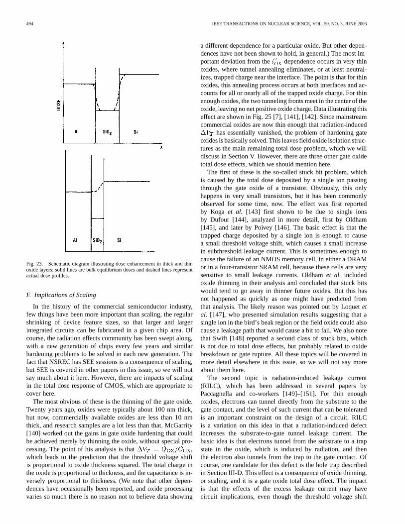
Dose enhancement has been known and studied for manyyears, but it is a practical problem because of the widespreaduse of low energy (10 keV) X-ray sources. For a photonsource (X-ray or gamma), most of the energy deposition isactually done by secondary electrons. The critical conceptis called charged particle equilibrium (CPE). Normally, in ahomogeneous slab of material, CPE is maintained because thenumber of secondary electrons scattering into any incrementof volume is equal to the number of electrons scattering out.The problem in an MOS device is illustrated in Fig. 23 [17],where there are several thin layers of different compositionsand, therefore, different cross sections. CPE is not maintainedbecause more secondary electrons cross an interface from thehigh-Z side than from the low-Z side. In Fig. 23, the solidlines indicate the deposition profile that would be predicted for10 keV X-rays, using the mass absorption coefficients alone,without any secondary electron transport. Fig. 23(a) indicatesthe situation when the oxide is thick compared to the rangeof the secondary electrons, where the broken line indicatesthe change in the depth-dose profile from the transport ofsecondary electrons into the oxide layer. The situation for athin oxide is illustrated in Fig. 23(b), where the electrons go allthe way through the oxide layer, and the dose-enhancement isindicated by the broken line. Dose enhancement as a functionof oxide thickness is indicated in Fig. 24 [17], [135]–[137]. Fortesting with an X-ray source, dose enhancement is an importanteffect, which means that the dose is different in different partsof the structure (e.g., gate oxides and field oxides). On the otherhand, in a Co source, the mass absorption coefficient for allthe materials shown in Fig. 23 is essentially equal, and the doseis uniform because CPE is maintained [17], [18], [136], [137].Dosimetry, in general, is covered in a separate paper in thisissue [139], so we will not discuss it further here.
494 IEEE TRANSACTIONS ON NUCLEAR SCIENCE, VOL. 50, NO. 3, JUNE 2003
Fig. 23. Schematic diagram illustrating dose enhancement in thick and thinoxide layers; solid lines are bulk equilibrium doses and dashed lines representactual dose profiles.
F. Implications of Scaling
In the history of the commercial semiconductor industry,few things have been more important than scaling, the regularshrinking of device feature sizes, so that larger and largerintegrated circuits can be fabricated in a given chip area. Ofcourse, the radiation effects community has been swept along,with a new generation of chips every few years and similarhardening problems to be solved in each new generation. Thefact that NSREC has SEE sessions is a consequence of scaling,but SEE is covered in other papers in this issue, so we will notsay much about it here. However, there are impacts of scalingin the total dose response of CMOS, which are appropriate tocover here.
The most obvious of these is the thinning of the gate oxide.Twenty years ago, oxides were typically about 100 nm thick,but now, commercially available oxides are less than 10 nmthick, and research samples are a lot less than that. McGarrity[140] worked out the gains in gate oxide hardening that couldbe achieved merely by thinning the oxide, without special pro-cessing. The point of his analysis is that ,which leads to the prediction that the threshold voltage shiftis proportional to oxide thickness squared. The total charge inthe oxide is proportional to thickness, and the capacitance is in-versely proportional to thickness. (We note that other depen-dences have occasionally been reported, and oxide processingvaries so much there is no reason not to believe data showing
a different dependence for a particular oxide. But other depen-dences have not been shown to hold, in general.) The most im-portant deviation from the dependence occurs in very thinoxides, where tunnel annealing eliminates, or at least neutral-izes, trapped charge near the interface. The point is that for thinoxides, this annealing process occurs at both interfaces and ac-counts for all or nearly all of the trapped oxide charge. For thinenough oxides, the two tunneling fronts meet in the center of theoxide, leaving no net positive oxide charge. Data illustrating thiseffect are shown in Fig. 25 [7], [141], [142]. Since mainstreamcommercial oxides are now thin enough that radiation-induced
has essentially vanished, the problem of hardening gateoxides is basically solved. This leaves field oxide isolation struc-tures as the main remaining total dose problem, which we willdiscuss in Section V. However, there are three other gate oxidetotal dose effects, which we should mention here.
The first of these is the so-called stuck bit problem, whichis caused by the total dose deposited by a single ion passingthrough the gate oxide of a transistor. Obviously, this onlyhappens in very small transistors, but it has been commonlyobserved for some time, now. The effect was first reportedby Koga et al. [143] first shown to be due to single ionsby Dufour [144], analyzed in more detail, first by Oldham[145], and later by Poivey [146]. The basic effect is that thetrapped charge deposited by a single ion is enough to causea small threshold voltage shift, which causes a small increasein subthreshold leakage current. This is sometimes enough tocause the failure of an NMOS memory cell, in either a DRAMor in a four-transistor SRAM cell, because these cells are verysensitive to small leakage currents. Oldhamet al. includedoxide thinning in their analysis and concluded that stuck bitswould tend to go away in thinner future oxides. But this hasnot happened as quickly as one might have predicted fromthat analysis. The likely reason was pointed out by Loquetetal. [147], who presented simulation results suggesting that asingle ion in the bird’s beak region or the field oxide could alsocause a leakage path that would cause a bit to fail. We also notethat Swift [148] reported a second class of stuck bits, whichis not due to total dose effects, but probably related to oxidebreakdown or gate rupture. All these topics will be covered inmore detail elsewhere in this issue, so we will not say moreabout them here.
The second topic is radiation-induced leakage current(RILC), which has been addressed in several papers byPaccagnella and co-workers [149]–[151]. For thin enoughoxides, electrons can tunnel directly from the substrate to thegate contact, and the level of such current that can be toleratedis an important constraint on the design of a circuit. RILCis a variation on this idea in that a radiation-induced defectincreases the substrate-to-gate tunnel leakage current. Thebasic idea is that electrons tunnel from the substrate to a trapstate in the oxide, which is induced by radiation, and thenthe electron also tunnels from the trap to the gate contact. Ofcourse, one candidate for this defect is the hole trap describedin Section III-D. This effect is a consequence of oxide thinning,or scaling, and it is a gate oxide total dose effect. The impactis that the effects of the excess leakage current may havecircuit implications, even though the threshold voltage shift
OLDHAM AND M CLEAN: TOTAL IONIZING DOSE EFFECTS IN MOS OXIDES AND DEVICES 495
Fig. 24. Measured and calculated dose enhancement as a function of oxide thickness for 10 keV X-rays [8].
Fig. 25. Threshold and flatband voltage shifts per unit dose as a function ofoxide thickness at 80 K. Dashed line is thickness squared; solid line and pointsare experimental results [142].
is insignificant. RILC may also be related to breakdown inthe oxide because it has been argued that leakage currentscontribute to oxide wearout, which in turn leads to breakdown.But, a discussion of breakdown is beyond the scope of thispaper.
The third topic is mobility degradation—even though the totalshift in threshold voltage is small, defects close enough to theinterface can reduce carrier mobility by acting as scattering cen-
ters. For interface traps, this effect was originally identified andanalyzed by Sun and Plummer [152]. Their work was extendedto also include the effect of oxide trapped holes by McLean andBoesch, Jr. [153]. Generally, interface traps will cause a largereffect at late times, but the effect of hole traps is detectable insome experiments.
V. RADIATION -INDUCED FIELD OXIDE LEAKAGE CURRENTS
For much of the recent history of the NSREC, the main totaldose problem in MOS technology has been damage to fieldoxide isolation structures, which has often meant local oxida-tion of silicon (LOCOS) structures, as shown in Fig. 26 [154].Charge buildup in the thick field oxide, or the bird’s beak re-gion, or both, turns on a parasitic leakage path. Current flowsfrom source-to-drain, outside the active gate region, as indicatedin the figure. Experimentally, the effect of such a leakage pathon the – characteristic of a device is illustrated in Fig. 27.
The initial – characteristic of a transistor is shown, alongwith the small shift it undergoes when irradiated; the shift issmall because the oxide is relatively thin. There is also a par-asitic field oxide device curve which is not visible experimen-tally, initially, because it is far to the right of the gate character-istic. But the field oxide is much thicker than the gate oxide, sothe shift per unit dose is much larger and the curve eventuallyshifts past the gate characteristic. In the illustration, the post-ra-diation field oxide curve is on the left side of the figure. Themeasured – curve, postradiation, is indicated by the brokenline, labeled “combined.” The leakage current at 0 V increasesfrom the prerad value by several orders of magnitude, which isoften enough to cause functional failure of a circuit. Oldhametal. [154] and Terrellet al. [155] have reported on the radiationresponse, including annealing, of several commercial field ox-ides, and there is wide variation in the results. It is basicallyimpossible to predict the response of such an oxide, without
496 IEEE TRANSACTIONS ON NUCLEAR SCIENCE, VOL. 50, NO. 3, JUNE 2003
Fig. 26. Schematic illustration of LOCOS field oxide isolation structure.
Fig. 27. Schematic illustration of theI–V characteristic of an n-channelMOSFET and parasitic leakage transistor before and after irradiation. Theparasitic device has much greater oxide thickness and larger shift so that itdominates the overall response after irradiation.
studying the particular oxide in question. Some of them do an-neal on a reasonable time-scale, which can be very useful insome applications (in space, for example).
As feature sizes were scaled below about 0.35m, theLOCOS approach became less effective, and the emphasis inthe industry shifted to trench isolation schemes. But trenchprocesses vary so widely, it is difficult to make general state-ments about them. Both LOCOS structures and trenches canbe hardened [156], with sufficient investment, but the detailscannot generally be discussed in the open literature. Thecompanies consider these process details proprietary.
VI. CONCLUSION
We have reviewed the total ionizing dose radiation responseof MOS materials, devices, and circuits. Generally, the responseis very complex, with many different physical processes con-tributing. Each of these processes has a different time depen-dence, a different field dependence, and a different temperature
dependence. Even though the overall, combined response is ex-tremely complex, a high level of understanding has now beenachieved by isolating the different mechanisms and by studyingthem one at a time. The study of these mechanisms has been amajor theme of the NSREC throughout most of its 40-year his-tory. The understanding that has been achieved stands as a majorsuccess for the conference and the conference community.
ACKNOWLEDGMENT
The authors wish to thank K. LaBel and L. Cohn for theirsupport and M. O’Bryan for technical assistance in preparingthe final manuscript.
REFERENCES
[1] T. P. Ma and P. V. Dressendorfer,Ionizing Radiation Effects in MOSDevices and Circuits. New York: Wiley-Interscience, 1989.
[2] T. R. Oldham,Ionizing Radiation Effects in MOS Oxides, Advancesin Solid State Electronics and Technology (ASSET) Series, Singapore:World Scientific, 1999.
[3] R. C. Hughes, “Charge carrier transport phenomena in amorphous SiO:Direct measurement of mobility and carrier lifetime,”Phys. Rev. Lett.,vol. 30, p. 1333, 1973.
[4] G. A. Ausman and F. B. McLean, “Electron-hole pair creation energy inSiO ,” Appl. Phys. Lett., vol. 26, p. 173, 1975.
[5] O. L. Curtis, J. R. Srour, and K. Y. Chiu, “Hole and electron transport inSiO films,” J. Appl. Phys., vol. 45, p. 406, 1974.
[6] H. H. Sander and B. L. Gregory, “Unified model of damage annealing inCMOS, from freeze-in to transient annealing,”IEEE Trans. Nucl. Sci.,vol. NS-22, p. 2157, 1975.
[7] H. E. Boesch, Jr. and J. M. McGarrity, “Charge yield and dose effects at80 K,” IEEE Trans. Nucl. Sci., vol. NS-23, p. 1520, 1976.
[8] J. M. Benedetto and H. E. Boesch, Jr., “The relationship between Coand 10 keV X-ray damage in MOS devices,”IEEE Trans. Nucl. Sci., vol.NS-33, p. 1318, 1986.
[9] M. von Smoluchowski, “Uber brownsche molekularbewegung unter ein-wirkung ausserer krafte und deren zusammenhang mit der verallgemein-erter diffusionsgleichung,”Annalen der Physik, vol. 44, p. 1103, 1915.
[10] L. Onsager, “Initial recombination of ions,”Phys. Rev., vol. 54, p. 554,1938.
[11] G. A. Ausman, “Field dependence of geminate recombination in adielectric medium,”, Adelphi, MD, Harry Diamond Lab. Tech. Rep.HDL-TR-2097, 1987.
[12] G. Jaffe,Zur Theorie der Ionization in Kolonnen: Annalen der Physik,1913, vol. 42, p. 303.
[13] P. Langevin, “L’Ionization de gaz,”Ann. Chim. Phys., vol. 28, p. 289,1903.
[14] T. R. Oldham and J. M. McGarrity, “Ionization of SiOby heavy chargedparticles,”IEEE Trans. Nucl. Sci., vol. NS-28, p. 3975, 1981.
[15] T. R. Oldham, “Charge generation and recombination in silicon dioxidefrom heavy charged particles,”, Adelphi, MD, Harry Diamond Lab.Tech. Rep. HDL-TR-1985, 1982.
[16] , “Recombination along the tracks of heavy charged particles inSiO films,” J. Appl. Phys., vol. 57, p. 2695, 1985.
[17] T. R. Oldham and J. M. McGarrity, “Comparison of Coand 10 keVX-ray response in MOS capacitors,”IEEE Trans. Nucl. Sci., vol. NS-30,p. 4377, 1983.
[18] C. M. Dozier and D. B. Brown, “Effect of photon energy on the responseof MOS devices,”IEEE Trans. Nucl. Sci., vol. NS-28, p. 4137, 1981.
[19] M. R. Shaneyfelt, D. M. Fleetwood, J. R. Schwank, and K. L. Hughes,“Charge yield for Co-60 and 10-keV X-ray irradiations of MOS de-vices,” IEEE Trans. Nucl. Sci., vol. NS-38, p. 1187, 1991.
[20] T. R. Oldham, “Analysis of damage in MOS devices for several radiationenvironments,”IEEE Trans. Nucl. Sci., vol. NS-31, p. 1236, 1984.
[21] E. G. Stassinopoulos, G. J. Brucker, O. Van Gunten, A. R. Knudsen, andT. M. Jordan, “Radiation effects on MOS devices: Dosimetry, annealing,irradiation sequence and sources,”IEEE Trans. Nucl. Sci., vol. NS-30,p. 1880, 1983.
[22] E. G. Stassinopoulos, O. Van Gunten, G. J. Brucker, A. R. Knudsen, andT. M. Jordan, “The damage equivalence of electrons, protons, alphas,and gamma rays in rad-hard MOS devices,”IEEE Trans. Nucl. Sci., vol.NS-30, p. 4363, 1983.
OLDHAM AND M CLEAN: TOTAL IONIZING DOSE EFFECTS IN MOS OXIDES AND DEVICES 497
[23] E. G. Stassinopoulos, G. J. Brucker, and O. Van Gunten, “Total dose anddose rate dependence of proton damage in MOS devices during and afterirradiation,” IEEE Trans. Nucl. Sci., vol. NS-31, p. 1444, 1984.
[24] G. J. Brucker, E. G. Stassinopoulos, O. Van Gunten, L. S. August, andT. M. Jordan, “The damage equivalence of electrons, protons, andgamma rays in MOS devices,”IEEE Trans. Nucl. Sci., vol. NS-29,p. 1966, 1982.
[25] G. J. Brucker, O. Van Gunten, E. G. Stassinopoulos, P. Shapiro, L. S. Au-gust, and T. M. Jordan, “Recovery of damage in rad-hard MOS devicesduring and after irradiation by electrons, protons, alphas, and gammarays,” IEEE Trans. Nucl. Sci., vol. NS-30, p. 4157, 1983.
[26] W. J. Stapor, L. S. August, D. H. Wilson, T. R. Oldham, and K. M.Murray, “Proton and heavy ion damage studies in MOS transistors,”IEEE Trans. Nucl. Sci., vol. NS-32, p. 4399, 1985.
[27] R. L. Pease, M. Simons, and P. Marshall, “Comparison of PMOSFETresponse for Co gammas and high energy protons,”J. Radiation Ef-fects Res. Eng., vol. 18, p. 126, 2000.
[28] P. Paillet, J. R. Schwank, M. Shaneyfelt, V. Ferlet-Cavrois, R. A.Loemker, and O. Flament, “Comparison of charge yield in MOSdevices for different radiation sources,”IEEE Trans. Nucl. Sci., vol. 49,p. 2656, 2002.
[29] H. E. Boesch, Jr., F. B. McLean, J. M. McGarrity, and G. A. Ausman,“Hole transport and charge relaxation in irradiated SiOMOS capaci-tors,” IEEE Trans. Nucl. Sci., vol. NS-22, p. 2163, 1975.
[30] R. C. Hughes, “Hole mobility and transport in thin SiOfilms,” Appl.Phys. Lett., vol. 26, p. 436, 1975.
[31] R. C. Hughes, E. P. EerNisse, and H. J. Stein, “Hole transport in MOSoxides,”IEEE Trans. Nucl. Sci., vol. NS-22, p. 2227, 1975.
[32] F. B. McLean, G. A. Ausman, H. E. Boesch, Jr., and J. M. McGarrity,“Application of stochastic hopping transport to hole conduction in amor-phous SiO,” J. Appl. Phys., vol. 47, p. 1529, 1976.
[33] F. B. McLean, H. E. Boesch, Jr., and J. M. McGarrity, “Hole transportand recovery characteristics of SiOgate insulators,”IEEE Trans. Nucl.Sci., vol. NS-23, p. 1506, 1976.
[34] J. R. Srour, S. Othmer, O. L. Curtis, and K. Y. Chiu, “Radiation-inducedcharge transport and charge build-up in SiOfilms at low temperatures,”IEEE Trans. Nucl. Sci., vol. NS-23, p. 1513, 1976.
[35] O. L. Curtis and J. R. Srour, “The multiple trapping model and holetransport in SiO,” J. Appl. Phys., vol. 48, p. 3819, 1977.
[36] R. C. Hughes, “Time-resolved hole transport in a-SiO,” Phys. Rev., vol.B15, p. 2012, 1977.
[37] F. B. McLean, H. E. Boesch, Jr., and J. M. McGarrity, “Field-dependenthole transport in amorphous SiO,” in The Physics of SiOand Its In-terfaces, S. T. Pantelides, Ed. New York: Pergamon, 1978, p. 19.
[38] H. E. Boesch, Jr., J. M. McGarrity, and F. B. McLean, “Temperature andfield-dependent charge relaxation in SiOgate insulators,”IEEE Trans.Nucl. Sci., vol. NS-25, p. 1012, 1978.
[39] H. E. Boesch, Jr., F. B. McLean, J. M. McGarrity, and P. S. Winokur,“Enhanced flatband voltage recovery in hardened thin MOS capacitors,”IEEE Trans. Nucl. Sci., vol. NS-25, p. 1239, 1978.
[40] H. E. Boesch, Jr. and F. B. McLean, “Hole transport and trapping in fieldoxides,”IEEE Trans. Nucl. Sci., vol. NS-32, p. 3940, 1985.
[41] E. W. Montroll and G. H. Weiss, “Random walks on lattices ii,”J. Math.Phys., vol. 6, p. 167, 1965.
[42] H. Scher and M. Lax, “Stochastic transport in a disordered solid,”I-Theory, Phys. Rev., vol. B7, p. 4491, 1973.
[43] , “Stochastic transport in a disordered solid,”II-Impurity Conduc-tion, Phys. Rev., vol. B7, p. 4502, 1973.
[44] G. Pfister and H. Scher, “Dispersive (non-Gaussian) transient transportin disordered solids,”Adv. Phys., vol. 27, p. 747, 1978.
[45] N. F. Mott and E. A. Davis,Electronic Processes in Non-CrystallineMaterials, 2nd ed. Oxford, U.K.: Clarendon, 1979, p. 65.
[46] I. G. Austin and N. F. Mott, “Polarons in crystalline and noncrystallinematerials,”Adv. Phys., vol. 18, p. 41, 1969.
[47] D. Emin, “Phonon-assisted transition rates I-optical-phonon-assistedhopping in solids,”Adv. Phys., vol. 24, p. 305, 1975.
[48] B. E. Deal, M. Sklar, A. S. Grove, and E. H. Snow, “Characteristicsof surface-state charge (QSS) of thermally oxidized silicon,”J. Elec-trochem. Soc., vol. 114, p. 266, 1967.
[49] F. J. Feigl, W. B. Fowler, and K. L. Yip, “Oxygen vacancy model for theE ’ center in SiO ,” Solid State Commun., vol. 14, p. 225, 1974.
[50] R. A. Weeks, “Paramagnetic resonance of defects in irradiated quartz,”J. Appl. Phys., vol. 27, p. 1376, 1956.
[51] P. M. Lenahan and P. V. Dressendorfer, “Hole traps and trivalent siliconcenters in metal/oxide/silicon devices,”J. Appl. Phys., vol. 55, p. 3495,1984.
[52] F. B. McLean, “A direct tunneling model of charge transfer at the in-sulator semiconductor interface in MIS devices,” Harry Diamond Lab.,HDL-TR-1765, 1976.
[53] G. F. Derbenwick and H. H. Sander, “CMOS hardness prediction forlow-dose-rate environments,”IEEE Trans. Nucl. Sci., vol. NS-24, p.2244, 1977.
[54] P. S. Winokur, “Limitations in the use of linear systems theory for theprediction of hardened-MOS device response in space satellite environ-ments,”IEEE Trans. Nucl. Sci., vol. NS-29, p. 2102, 1982.
[55] P. S. Winokur, K. G. Kerris, and L. Harper, “Predicting CMOS inverterresponse in nuclear and space environments,”IEEE Trans. Nucl. Sci.,vol. NS-30, p. 4326, 1983.
[56] S. Manzini and A. Modelli, “Tunneling discharge of trapped holes insilicon dioxide,” in Insulating Films in Semiconductors, J. F. Verweijand D. R. Wolters, Eds. North Holland, The Netherlands: Elsevier Sci.,1983, p. 112.
[57] T. R. Oldham, A. J. Lelis, and F. B. McLean, “Spatial dependenceof trapped holes determined from tunneling analysis and measuredannealing,”IEEE Trans. Nucl. Sci., vol. NS-33, p. 1203, 1986.
[58] V. Lakshmanna and A. S. Vengurlekar, “Logarithmic detrappingresponse for holes injected into SiOand the influence of thermalactivation and electric fields,”J. Appl. Phys., vol. 63, p. 4548, 1988.
[59] M. Simons and H. L. Hughes, “Determining the energy distributionof pulsed-radiation- induced charge in MOS structures from rapidannealing measurements,”IEEE Trans. Nucl. Sci., vol. NS-19, p. 282,Dec. 1972.
[60] , “Short-Term Charge Annealing in Electron-Irradiated SiliconDioxide,” IEEE Trans. Nucl. Sci., vol. NS-18, p. 106, Dec. 1971.
[61] J. G. Simmons and G. W. Taylor, “High-field isothermal currents andthermally stimulated currents in insulators having discrete trappinglevels,”Phys. Rev., vol. B5, p. 1619, 1972.
[62] Z. Shanfield, “Thermally stimulated current measurements on irradiatedMOS capacitors,”IEEE Trans. Nucl. Sci., vol. NS-30, p. 4377, 1983.
[63] Z. Shanfield and M. Moriwaki, “Radiation-induced hole trapping andinterface state characteristics of al-gate and poly-si gate MOS capaci-tors,” IEEE Trans. Nucl. Sci., vol. NS-32, p. 3929, 1985.
[64] , “Characteristics of hole traps in dry and pyrogenic gate oxides,”IEEE Trans. Nucl. Sci., vol. NS-31, p. 1242, 1984.
[65] D. M. Fleetwood, R. A. Reber, and P. S. Winokur, “Effect of bias onthermally stimulated curent (TSC) in irradiated MOS devices,”IEEETrans. Nucl. Sci., vol. 38, p. 1066, 1991.
[66] D. M. Fleetwood, S. L. Miller, R. A. Reber, P. J. McWhorter, P. S.Winokur, M. R. Shaneyfelt, and J. R. Schwank, “New insights into radia-tion-induced oxide-trapped charge through thermally stimulated currentmeasurement and analysis,”IEEE Trans. Nucl. Sci., vol. 39, p. 2192,1992.
[67] D. M. Fleetwood, M. R. Shaneyfelt, L. C. Riewe, P. S. Winokur, andR. A. Reber, “The role of border traps in MOS high-temperature post-irradiation annealing response,”IEEE Trans. Nucl. Sci., vol. 40, p. 1323,1993.
[68] D. M. Fleetwood, P. S. Winokur, R. A. Reber, T. L. Meisenheimer, J. R.Schwank, M. R. Shaneyfelt, and J. R. Schwank, “Effects of oxide traps,interface traps, and border traps on MOS devices,”J. Appl. Phys., vol.73, p. 5058, 1993.
[69] D. M. Fleetwood, “Revised model of thermally stimulated current inMOS capacitors,”IEEE Trans. Nucl. Sci., vol. 44, p. 1826, 1997.
[70] P. J. McWhorter, S. L. Miller, and W. M. Miller, “Modeling the annealof radiation-induced trapped holes in a varying thermal environment,”IEEE Trans. Nucl. Sci, vol. 37, p. 1682, 1990.
[71] P. J. McWhorter, S. L. Miller, and T. A. Dellin, “Modeling the memoryretention characteristics of SNOS nonvolatile transistors in a varyingthermal environment,”J. Appl. Phys., vol. 68, p. 1902, 1990.
[72] J. R. Schwank, P. S. Winokur, P. J. McWhorter, F. W. Sexton, P. V.Dressendorfer, and D. C. Turpin, “Physical mechanisms contributing todevice “Rebound,”IEEE Trans. Nucl. Sci., vol. NS-31, p. 1434, 1984.
[73] C. M. Dozier, D. B. Brown, J. L. Throckmorton, and D. I. Ma, “Defectproduction in SiO by X-ray and Co-60 radiations,”IEEE Trans. Nucl.Sci, vol. NS-32, p. 4363, 1985.
[74] A. J. Lelis, H. E. Boesch, Jr., T. R. Oldham, and F. B. McLean, “Re-versibility of trapped hole annealing,”IEEE Trans. Nucl. Sci., vol. 35,p. 1186, 1988.
[75] A. J. Lelis, T. R. Oldham, H. E. Boesch, Jr., and F. B. McLean, “Thenature of the trapped hole annealing process,”IEEE Trans. Nucl. Sci.,vol. 36, p. 1808, 1989.
[76] A. J. Lelis and T. R. Oldham, “Time dependence of switching oxidetraps,”IEEE Trans. Nucl. Sci., vol. 41, p. 1835, 1994.
498 IEEE TRANSACTIONS ON NUCLEAR SCIENCE, VOL. 50, NO. 3, JUNE 2003
[77] R. K. Freitag, D. B. Brown, and C. M. Dozier, “Experimental evidencefor two species of radiation-induced trapped positive charge,”IEEETrans. Nucl. Sci., no. 40, p. 1316, 1993.
[78] , “Evidence for two types of radiation-induced trapped positivecharge,”IEEE Trans. Nucl. Sci., vol. 41, p. 1828, 1994.
[79] W. L. Warren, M. R. Shaneyfelt, D. M. Fleetwood, J. R. Schwank, P. S.Winokur, and R. A. B. Devine, “Microscopic nature of border traps inMOS oxides,”IEEE Trans. Nucl. Sci., vol. 41, p. 1817, 1994.
[80] A. H. Edwards and W. B. Fowler, “Final Rep.–ONR Contract,”,N00014-92-J-2001, 1995.
[81] M. Walters and A. Reisman, “Radiation-induced neutral electron trapgeneration in electrically biased insulated gate field effect transistor gateinsulators,”J. Electrochem. Soc., vol. 138, p. 2756, 1991.
[82] J. F. Conley, P. M. Lenahan, A. J. Lelis, and T. R. Oldham, “Electron spinresonance evidence for the structure of a switching oxide trap: Long termstructural change at silicon dangling bond sites in SiO,” Appl. Phys.Lett., vol. 67, p. 2179, 1995.
[83] , “Electron spin resonance evidenceE centers can behave asswitching oxide traps,”IEEE Trans. Nucl. Sci., vol. 42, p. 1744, 1995.
[84] S. P. Karna, A. C. Pineda, R. D. Pugh, W. M. Shedd, and T. R. Oldham,“Electronic structure theory and mechanisms of the oxide trapped holeannealing process,”IEEE Trans. Nucl. Sci., vol. 47, p. 2316, 2000.
[85] C. J. Nicklaw, Z. Y. Lu, D. M. Fleetwood, R. D. Schrimpf, and S. T. Pan-telides, “The structure, properties, and dynamics of oxygen vacancies inamorphous SiO,” IEEE Trans. Nucl. Sci., vol. 49, p. 2667, 2002.
[86] D. M. Fleetwood, H. D. Xiong, R. D. Schrimpf, Z. Y. Lu, S. T. Pantelides,and C. J. Nicklaw, “Unified model of hole trapping, charge neutraliza-tion, and1=f noise in MOS devices,”IEEE Trans. Nucl. Sci., vol. 49,p. 2674, 2002.
[87] D. M. Fleetwood, “Border traps in MOS devices,”IEEE Trans. Nucl.Sci., vol. 39, p. 269, 1992.
[88] D. M. Fleetwood, W. L. Warren, J. R. Schwank, P. S. Winokur, M. R.Shaneyfelt, and L. C. Riewe, “Effects of interface traps and border trapson MOS post-irradiation annealing response,”IEEE Trans. Nucl. Sci.,vol. 42, p. 1698, 1995.
[89] P. M. Lenahan and P. V. Dressendorfer, “An electron spin resonancestudy of radiation-induced electrically active paramagnetic centers at theSi/SiO interface,”J. Appl. Phys., vol. 54, p. 1457, 1983.
[90] T. R. Oldham, F. B. McLean, H. E. Boesch, Jr., and J. M. McGarrity,“An overview of radiation-induced interface traps in MOS structures,”Semiconduct. Sci. Technol., vol. 4, p. 986, 1989.
[91] A. J. Lelis, T. R. Oldham, and W. M. Delancey, “Response of interfacetraps during high-temperature anneals,”IEEE Trans. Nucl. Sci., vol. 38,p. 1590, 1991.
[92] F. B. McLean, “A framework for understanding radiation-induced inter-face states in MOS SiOstructures,”IEEE Trans. Nucl. Sci., vol. NS-27,p. 1651, 1980.
[93] H. E. Boesch, Jr., F. B. McLean, J. M. McGarrity, and G. A. Ausman,“Hole transport and charge relaxation in irradiated SiOMOS capaci-tors,” IEEE Trans. Nucl. Sci., vol. NS-22, p. 2163, 1975.
[94] P. S. Winokur and M. A. Sokoloski, “Comparison of interface statebuild-up in MOS capacitors subject to penetrating and nonpenetratingradiation,”Appl. Phys. Lett., vol. 28, p. 627, 1975.
[95] P. S. Winokur, J. M. McGarrity, and H. E. Boesch, Jr., “Dependenceof interface-state buildup on hole generation and transport in irradiatedMOS capacitors,”IEEE Trans. Nucl. Sci., vol. NS-23, p. 1580, 1976.
[96] P. S. Winokur, H. E. Boesch, Jr., J. M. McGarrity, and F. B. McLean,“Field- and time-dependent radiation effects at the Si/SiOinterface ofhardened MOS capacitors,”IEEE Trans. Nucl. Sci., vol. NS-24, p. 2113,1977.
[97] , “Two stage process for the buildup of radiation-induced interfacetraps,”J. Appl. Phys., vol. 50, p. 3492, 1979.
[98] P. S. Winokur and H. E. Boesch, Jr., “Interface state generation in radi-ation-hard oxides,”IEEE Trans. Nucl. Sci., vol. NS-27, p. 1647, 1980.
[99] J. M. McGarrity, P. S. Winokur, H. E. Boesch, Jr., and F. B. McLean,Interface States Resulting from a Hole Flux Incident on the Si/SiOIn-terface, Physics of SiOand Its Interfaces, S. T. Pantelides, Ed. NewYork: Pergamon, 1978, p. 428.
[100] H. E. Boesch, Jr. and F. B. McLean, “Interface state generation associ-ated with hole transport in MOS structures,”J. Appl. Phys., vol. 60, p.448, 1986.
[101] P. S. Winokur, F. B. McLean, and H. E. Boesch, Jr., “Physical processesassociated with radiation-induced interface states,” U. S. Army HarryDiamond Lab., Adelphi, MD, HDL-TR-2081, 1986.
[102] N. S. Saks and M. C. Ancona, “Time dependence of interface trap for-mation in MOSFET’s following pulsed irradiation,”IEEE Trans. Nucl.Sci., vol. NS-34, p. 1348, 1987.
[103] N. S. Saks, C. M. Dozier, and D. B. Brown, “Time dependence of inter-face trap formation in MOSFET’s following pulsed irradiation,”IEEETrans. Nucl. Sci., vol. 35, p. 1168, 1988.
[104] N. S. Saks, R. B. Klein, and D. L. Griscom, “Formation of interface trapsin MOSFET’s during annealing following low temperature radiation,”IEEE Trans. Nucl. Sci., vol. 35, p. 1234, 1988.
[105] N. S. Saks and D. B. Brown, “Interface trap formation via the two stageH process,”IEEE Trans. Nucl. Sci, vol. 36, p. 1848, 1989.
[106] , “Observation of H motion during interface trap formation,”IEEE Trans. Nucl. Sci., vol. 37, p. 1624, 1990.
[107] N. S. Saks and R. W. Rendell, “Time dependence of post-irradiationinterface trap build-up in deuterium annealed oxides,”IEEE Trans. Nucl.Sci., vol. 39, p. 2220, 1992.
[108] N. S. Saks, R. B. Klein, R. E. Stahlbush, B. J. Mrstik, and R. W. Rendell,“Effect of post-stress hydrogen annealing on MOS oxides after Coirradiation or fowler-nordheim injection,”IEEE Trans. Nucl. Sci., vol.40, p. 1341, 1993.
[109] S. R. Hofstein, “Proton and sodium transport in SiOfilms,” IEEETrans. Electron. Devices, vol. ED-14, p. 749, 1967.
[110] H. E. Boesch, Jr., “Time dependent interface trap effects in MOS de-vices,” IEEE Trans. Nucl. Sci., vol. 35, p. 1160, 1988.
[111] D. L. Griscom, “Diffusion of radiolytic molecular hydrogen as a mech-anism for the post-irradiation build-up of interface states in SiO-on-Sistructures,”J. Appl. Phys., vol. 58, p. 2524, 1985.
[112] D. B. Brown, “The time dependence of interface state production,”IEEETrans. Nucl. Sci., vol. NS-32, p. 3900, 1985.
[113] D. L. Griscom, D. B. Brown, and N. S. Saks,Nature of Radiation-Induced Point Defects in Amorphous SiOand Their Role inSiO -on-Si Structures, The Physics and Chemistry of SiOandthe Si/SiO Interface, C. R. Helms and B. E. Deal, Eds. New York:Plenum, 1988.
[114] F. J. Grunthaner, B. F. Lewis, N. Z. amd, and J. Maserjian, “XPS studiesof structure-induced radiation defects at the Si/SiOinterface,” IEEETrans. Nucl. Sci., vol. NS-27, p. 1640, 1980.
[115] F. J. Grunthaner, P. J. Grunthaner, and J. Maserjian, “Radiation-induceddefects in SiO as determined with XPS,”IEEE Trans. Nucl. Sci., vol.NS-29, p. 1462, 1982.
[116] F. J. Grunthaner and P. J. Grunthaner, “Chemical and electronic structureof the SiO =Si interface,” inMaterial Science Report. Amsterdam,The Netherlands: North Holland, 1986, vol. 1, p. 65.
[117] S. K. Lai, “Interface trap generation in silicon dioxide when electronsare captured by trapped holes,”J. Appl. Phys., vol. 54, p. 2540, 1983.
[118] S. J. Wang, J. M. Sung, and S. A. Lyon, “Relation between hole trappingand interface state generation in metal-oxide-silicon structures,”Appl.Phys. Lett., vol. 52, p. 1431, 1988.
[119] D. M. Fleetwood, “Fast and slow border traps in MOS devices,”IEEETrans. Nucl. Sci., vol. 43, p. 779, 1996.
[120] J. R. Schwank, D. M. Fleetwood, M. R. Shaneyfelt, P. S. Winokur, C.L. Axeness, and L. C. Riewe, “Latent interface trap build-up and its im-plications for hardness assurance,”IEEE Trans. Nucl. Sci., vol. 39, p.1953, 1992.
[121] D. M. Fleetwood, P. S. Winokur, and T. L. Meisenheimer, “Hardnessassurance for low-dose space applications,”IEEE Trans. Nucl. Sci., vol.38, p. 1552, 1991.
[122] D. M. Fleetwood, P. S. Winokur, and J. R. Schwank, “Using laboratoryX-ray and cobalt-60 irradiations to predict CMOS device response instrategic and space environments,”IEEE Trans. Nucl. Sci., vol. 35, p.1497, 1988.
[123] F. B. McLean, “Generic impulse response function for MOS systemsand its application to linear response analysis,”IEEE Trans. Nucl. Sci.,vol. 35, p. 1178, 1988.
[124] A. H. Johnston, “Super recovery of total dose damage in MOS devices,”IEEE Trans. Nucl. Sci., vol. NS-31, p. 1427, 1984.
[125] H. E. Boesch, Jr., T. L. Taylor, L. R. Hite, and W. E. Bailey, “Time-dependent hole and electron trapping effects in SIMOX buried oxides,”IEEE Trans. Nucl. Sci., vol. 37, p. 1982, 1990.
[126] H. E. Boesch, Jr., T. L. Taylor, and G. A. Brown, “Charge build-up athigh dose and low fields in SIMOX buried oxides,”IEEE Trans. Nucl.Sci., vol. 38, p. 1234, 1991.
[127] E. W. Enlow, R. L. Pease, W. Coombs, R. D. Schrimpf, and R. N. Nowlin,“Response of advanced bipolar processes to ionizing radiation,”IEEETrans. Nucl. Sci., vol. 38, p. 1342, 1991.
[128] D. M. Fleetwood, S. L. Kosier, R. N. Nowlin, R. D. Schrimpf, R. A.Reber, M. DeLaus, P. S. Winokur, A. Wei, W. E. Coombs, and R. L.Pease, “Physical mechanisms contributing to enhanced bipolar gaindegradation at low dose rates,”IEEE Trans. Nucl. Sci., vol. 41, p. 1871,1994.
OLDHAM AND M CLEAN: TOTAL IONIZING DOSE EFFECTS IN MOS OXIDES AND DEVICES 499
[129] J. R. Schwank, “Radiation effects in SOI technologies,”IEEE Trans.Nucl. Sci., vol. 50, June 2003.
[130] R. L. Pease, “Total ionizing dose effects in bipolar devices and circuits,”IEEE Trans. Nucl. Sci., vol. 50, June 2003.
[131] P. S. Winokur, J. R. Schwank, P. J. McWhorter, P. V. Dressendorfer, andD. C. Turpin, “Correlating the radiation response of MOS capacitors andtransistors,”IEEE Trans. Nucl. Sci., vol. NS-31, p. 1453, 1984.
[132] P. J. McWhorter and P. S. Winokur, “Simple technique for separatingeffects of interface traps and oxide taps in metal-oxide-semiconductortransistors,”Appl. Phys. Lett., vol. 48, p. 133, 1986.
[133] P. J. McWhorter, D. M. Fleetwood, R. A. Pastorek, and G. T. Zim-merman, “Comparison of MOS capacitor and transistor post-irradiationresponse,”IEEE Trans. Nucl. Sci., vol. 36, p. 1792, 1989.
[134] P. M. Lenahan, N. A. Bohna, and J. P. Campbell, “Radiation-inducedinterface traps in MOS devices: Capture cross sections and the densityof states ofP silicon dangling bond centers,”IEEE Trans. Nucl. Sci.,vol. 49, p. 2708, 2002.
[135] C. M. Dozier and D. B. Brown, “Photon energy dependence of radiationeffects in MOS structures,”IEEE Trans. Nucl. Sci., vol. NS-27, p. 1694,1980.
[136] D. B. Brown, “The phenomenon of electron rollout for energy depositionand defect generation in irradiated MOS devices,”IEEE Trans. Nucl.Sci., vol. 33, p. 1240, 1986.
[137] C. M. Dozier and D. B. Brown, “The use of low energy X-rays for devicetesting-A comparison with Co-60 radiation,”IEEE Trans. Nucl. Sci., vol.NS-30, p. 4382, 1983.
[138] D. M. Fleetwood, D. E. Beutler, L. J. Lorence, D. B. Brown, B. L.Draper, L. C. Riewe, H. B. Rosenstock, and D. P. Knott, “Comparisonof enhanced device response and predicted X-ray dose enhancement ef-fects in MOS oxides,”IEEE Trans. Nucl. Sci., vol. 35, p. 1265, 1988.
[139] W. Beezholdet al., IEEE Trans. Nucl. Sci..[140] J. M. McGarrity, “Considerations for hardening MOS devices and cir-
[141] N. S. Saks, M. G. Ancona, and J. A. Modolo, “Radiation effects in MOScapacitors with very thin oxides at 80 K,”IEEE Trans. Nucl. Sci., vol.NS-31, p. 1249, 1984.
[142] J. M. Benedetto, H. E. Boesch, Jr., F. B. McLean, and J. P. Mize, “Holeremoval in thin gate MOSFET’s by tunneling,”IEEE Trans. Nucl. Sci.,vol. NS-32, p. 3916, 1985.
[143] R. Koga, W. R. Crain, K. B. Crawford, D. D. Lau, S. D. Pinkerton, B. K.Yi, and R. Chitty, “On the suitability of nonhardened high density sramsfor space applications,”IEEE Trans. Nucl. Sci., vol. 38, p. 1507, 1991.
[144] C. Dufour, P. Garnier, T. Carriere, J. Beaucour, R. Eccofet, and M.Labrunee, “Heavy ion induced single hard errors in submicronicmemories,”IEEE Trans. Nucl. Sci., vol. 39, p. 1693, 1992.
[145] T. R. Oldham, K. W. Bennett, J. Beaucour, T. Carriere, C. Poivey, and P.Garnier, “Total dose failures in advanced electronics from single ions,”IEEE Trans. Nucl. Sci., vol. 40, p. 1820, 1993.
[146] C. Poivey, T. Carriere, J. Beaucour, and T. R. Oldham, “Characterizationof single hard errors (SHE) in 1 M-bit srams from single ions,”IEEETrans. Nucl. Sci., vol. 41, p. 2235, 1994.
[147] J.-G. Loquet, J.-P. David, S. Duzellier, D. Falguere, and T. Nuns, “Sim-ulation of heavy-ion-induced failure modes in nMOS cells of ics,”IEEETrans. Nucl. Sci., vol. 48, p. 2278, 2001.
[148] G. M. Swift, D. J. Padgett, and A. H. Johnston, “A new class of singlehard errors,”IEEE Trans. Nucl. Sci., vol. 41, p. 2043, 1994.
[149] A. Scarpa, A. Paccagnella, F. Montera, G. Ghibaudo, G. Pananakakis, G.Ghidini, and P. G. Fuochi, “Ionizing radiation induced leakage currenton ultra-thin gate oxides,”IEEE Trans. Nucl. Sci., vol. 44, p. 1818, 1997.
[150] M. Ceschia, A. Paccagnella, A. Cester, A. Scarpa, and G. Ghidini, “Ra-diation induced leakage current and stress induced leakage current inultra-thin gate oxides,”IEEE Trans. Nucl. Sci., vol. 45, p. 2375, 1998.
[151] L. Larcher, A. Paccagnella, M. Ceschia, and G. Ghidini, “A model of ra-diation induced leakage current (RILC) in ultra-thin gate oxides,”IEEETrans. Nucl. Sci., vol. 46, p. 1553, 1999.
[152] S. C. Sun and J. D. Plummer, “Electron mobility in inversion and accu-mulation layers on thermally oxidized silicon surfaces,”IEEE J. Solid-State Circuits, vol. SC-15, p. 562, 1980.
[153] F. B. McLean and H. E. Boesch, Jr., “Time-dependent degradation ofMOSFET channel mobility followingpulsed irradiation,”IEEE Trans.Nucl. Sci., vol. 36, p. 1772, 1989.
[154] T. R. Oldham, A. J. Lelis, H. E. Boesch, Jr., J. M. Benedetto, F. B.McLean, and J. M. McGarrity, “Post-irradiation effects in field-oxideisolation structures,”IEEE Trans. Nucl. Sci., vol. 34, p. 1184, 1987.
[155] J. M. Terrell, T. R. Oldham, A. J. Lelis, and J. M. Benedetto, “Time-de-pendent annealing of radiation-induced leakage currents in MOS de-vices,” IEEE Trans. Nucl. Sci., vol. 36, p. 1808, 1989.
[156] M. R. Shaneyfelt, P. E. Dodd, B. L. Draper, and R. S. Flores, “Challengesin hardening technologies using shallow-trench isolation,”IEEE Trans.Nucl. Sci., vol. 45, p. 2584, 1998.