DEVICE DESCRIPTION The TRAC020 is the first universal Field Programmable Analog Device (FPAD) and provides a macro based solution to analog design problems using a unique mathematically based instruction set. Eight mathematical functions can be configured in up to 20 interconnected cells to facilitate the design and configuration of any analog circuit on-chip. Configuration takes place digitally via the integral CMOS shift register while the signal remains within the analog domain at all times avoiding sampling errors and processing delay found in equivalent DSP solutions. Performance is therefore equivalent to traditional solutions utilising conventional analog devices. Configuration is readily achieved through integration of the TRAC hardware and software. Designs are produced graphically using a simple, proprietary Windows TM ‘drag and drop’ user interface whilst simulation is carried out directly and instantaneously without leaving the design environment. Configuration of the hardware is achieved through a single mouse click to produce an instant analog circuit on-chip. APPLICATIONS Any analog circuit can be produced using TRAC. Typical examples include: • Filters • Multipliers • VCOs • PLLs • Precision Voltage References • Automatic Gain Control • Frequency to Voltage conversion etc. Features • User programmable • From design to silicon within the hour • A low risk and fast route from concept to silicon • For maximum flexibility each cell I/O can be connected externally • The function of each cell can be digitally programmed for LOG, ALOG, AUX, NON INVERTING PASS, NEGATE, ADD, RECTIFY and OFF • The device can be programmed with a standard EEPROM for non-microprocessor applications. • Device is offered in two package styles :- Small 36 pin SSOP package - production build 40 pin PDIP package - prototype build • The TRAC software and hardware fully integrates design, simulation and programming functions • For complex circuits the chips can be cascaded • The device is fully reconfigurable • High performance solution with signal path in analog domain • No sampling errors • Real time signal processing Ordering Information PART NUMBER PACKAGE PART MARK TRAC020SS36 SSOP36 TRAC020 TRAC020D40 PDIP40 TRAC020 TOTALLY RECONFIGURABLE ANALOG CIRCUIT Issue 3 - April 1997 TRAC020
Transcript
DEVICE DESCRIPTION
The TRAC020 is the first universal Field
Programmable Analog Device (FPAD) and
provides a macro based solution to analog
design problems using a unique
mathematically based instruction set. Eight
mathematical functions can be configured in
up to 20 interconnected cells to facilitate the
design and configuration of any analog circuit
on-chip.
Configuration takes place digitally via the
integral CMOS shift register while the signal
remains within the analog domain at all times
avoiding sampling errors and processing
delay found in equivalent DSP solutions.
Performance is therefore equivalent to
traditional solutions utilising conventional
analog devices.
Configuration is readily achieved through
integration of the TRAC hardware and
software. Designs are produced graphically
using a simple, proprietary WindowsTM
‘drag
and drop’ user interface whilst simulation is
carried out directly and instantaneously
without leaving the design environment.
Configuration of the hardware is achieved
through a single mouse click to produce an
instant analog circuit on-chip.
APPLICATIONS
Any analog circuit can be produced using
TRAC. Typical examples include:
• Filters
• Multipliers
• VCOs
• PLLs
• Precision Voltage References
• Automatic Gain Control
• Frequency to Voltage conversion etc.
Features
• User programmable
• From design to silicon within the hour
• A low risk and fast route from concept to
silicon
• For maximum flexibility each cell I/O can
be connected externally
• The function of each cell can be digitally
programmed for LOG, ALOG, AUX, NON
INVERTING PASS, NEGATE, ADD,
RECTIFY and OFF
• The device can be programmed with a
standard EEPROM for non-microprocessor
applications.
• Device is offered in two package styles :-
Small 36 pin SSOP package
- production build
40 pin PDIP package
- prototype build
• The TRAC software and hardware fully
integrates design, simulation and
programming functions
• For complex circuits the chips can be
cascaded
• The device is fully reconfigurable
• High performance solution with signal
path in analog domain
• No sampling errors
• Real time signal processing
Ordering Information
PART
NUMBER
PACKAGE PART
MARK
TRAC020SS36 SSOP36 TRAC020
TRAC020D40 PDIP40 TRAC020
TOTALLY RECONFIGURABLE ANALOG
CIRCUIT
Issue 3 - April 1997
TRAC020
ABSOLUTE MAXIMUM RATINGS
Voltage on any pin = 7.5V (relative to VSS)
Current in any IO/A1,A2 = 10mA
Power = 925 mW (PDIP 40)
Power = 925 mW (SSOP 36)
Operating Temperature = -40 to 125°C
Storage Temperature = -55 to 125°C
GENERAL ELECTRICAL CHARACTERISTICS
Test Conditions: Temperature = 25 °C, VDD = +2.5V, VSS = -2.5V,
Operating Temperature Range = -40 to 85°C
Operating Voltage Range = ± 2.5V ± 5%
PARAMETER CONDITIONS MIN TYPICAL MAX
Bandwidth 20mV peak-peak 4.0 MHz
Dynamic Range 80 dB
Noise Voltage 38
nV/Hz0.5
Total Harmonic Distortion 100mV peak-peak
1.0 V peak-peak
0.02%
0.08%
Intermodulation Distortion < 0.1%
Supply Rejection 60dB
Cell to cell crosstalk >60dB
Input common mode range
A1,A2
VDD
-1.0V,
VSS+1.5V
Output Swing ±1V
Supply Current All cells on 17mA 25mA 33mA
TRAC020
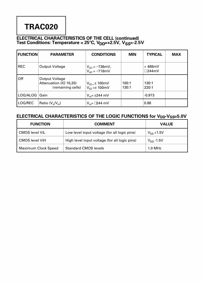
FUNCTION PARAMETER CONDITIONS MIN TYPICAL MAX
Non
Inverting
Pass
Internal Gain (IO/IO) VIO = ±100mV 0.9987 0.9997 1.00
External Gain (A1,A2) VIO = ±100mV 0.9971 0.9991 1.00
External Gain (IO5,6,15,16) VIO = ±100mV 0.9962 0.9982 1.00
External Gain (remaining cells) VIO = ±100mV 0.9948 0.9968 0.9988
Zetex GmbH Zetex Inc. Zetex (Asia) Ltd. These are supported byStreitfeldstraße 19 47 Mall Drive, Unit 4 3510 Metroplaza, Tower 2 agents and distributors inD-81673 München Commack NY 11725 Hing Fong Road, major countries world-wideGermany USA Kwai Fong, Hong Kong Zetex plc 1997Telefon: (49) 89 45 49 49 0 Telephone: (516) 543-7100 Telephone:(852) 26100 611Fax: (49) 89 45 49 49 49 Fax: (516) 864-7630 Fax: (852) 24250 494
This publication is issued to provide outline information only which (unless agreed by the Company in writing) may not be used, appliedor reproduced for any purpose or form part of any order or contract or be regarded as a representation relating to the products orservices concerned. The Company reserves the right to alter without notice the specification, design, price or conditions of supply of anyproduct or service.


![A Dynamically Reconfigurable ECG Analog Front-End with a 2.5 …bioee.ucsd.edu/papers/A Dynamically Reconfigurable ECG... · 2017-06-01 · State-of-the-art low power ECG AFEs [1-2]](https://static.documents.pub/doc/80x56/5f13579cde6f341989253c27/a-dynamically-reconfigurable-ecg-analog-front-end-with-a-25-bioeeucsdedupapersa.jpg)


