Towards 10 Gb/s orthogonal frequency divisionmultiplexing-based visible light communicationusing a GaN violet micro-LEDMOHAMED SUFYAN ISLIM,1,*,† RICARDO X. FERREIRA,2,† XIANGYU HE,2,† ENYUAN XIE,2 STEFAN VIDEV,3
SHAUN VIOLA,4 SCOTT WATSON,4 NIKOLAOS BAMIEDAKIS,5 RICHARD V. PENTY,5 IAN H. WHITE,5
ANTHONY E. KELLY,4 ERDAN GU,2 HARALD HAAS,3 AND MARTIN D. DAWSON2
1Li–Fi R&D Centre, the University of Edinburgh, Institute for Digital Communications, King’s Buildings, Mayfield Road, Edinburgh EH9 3JL, UK2Institute of Photonics, Department of Physics, University of Strathclyde, Glasgow G1 1RD, UK3Institute for Digital Communications, Li–Fi R&D Centre, the University of Edinburgh, King’s Buildings, Mayfield Road, Edinburgh EH9 3JL, UK4School of Engineering, University of Glasgow, Glasgow G12 8LT, UK5Centre for Advanced Photonics and Electronics, Electrical Engineering Division, Department of Engineering, University of Cambridge, CambridgeCB3 0FA, UK*Corresponding author: [email protected]
Received 28 November 2016; revised 9 February 2017; accepted 9 February 2017; posted 10 February 2017 (Doc. ID 280671);published 28 March 2017
The increasing demands of communication services are chal-lenging radio frequency (RF) wireless communications technol-ogies. The overall number of networked devices is expected toreach 26.3 billion in 2020 [1]. Visible light communication(VLC) is a promising solution to the limited availability of theRF spectrum as the visible light spectrum offers abundantbandwidth that is unlicensed and free to use. VLC improvesthe spectral efficiency per unit area, which enhances the qualityof service in crowded environments and allows for secure andlocalized services to be provided.
General lighting is under a rapid transformation to becomesemiconductor based due to huge energy savings. This trans-formation has already enabled applications such as active energyconsumption control and color tuning. Solid state lightingdevices such as gallium nitride (GaN)-based inorganic lightemitting diodes (LEDs) are ubiquitous power-efficient devicesto enable illumination and communications. Commercially
available LEDs have a limited frequency response due to theyellow phosphor coating on top of the blue LED chips. How-ever, the slow response of the yellow phosphor can be filteredout using a blue filter in front of the receiver. Recent resultsfor VLC using a phosphorescent white LED with adaptive bitand energy loading were reported at 2.32 Gb/s aided by a two-staged linear software equalizer [2].
Micro-LEDs are promising candidates in enabling lightingas a service (LaaS) and Internet of things (IoT). The introduc-tion of micro-LEDs has enabled high-performance value-addedlighting functions such as VLC and indoor positioning andtracking [3]. Micro-LEDs are known for their small active areasenabling high current density injection, which drives themodulation bandwidth to hundreds of megahertz [4,5]. At450 nm, micro-LEDs have set the standard for high-speedVLC. A 60 μm diameter pixel has achieved 3 Gb/s [6], andmore recently a single pixel of a new segmented array hasdemonstrated 5 Gb/s [7]. The novel micro-LEDs emitting at
Research Article Vol. 5, No. 2 / April 2017 / Photonics Research A35
400 nm featured in the current work offer a number of advan-tages over the 450 nm devices previously reported [7]. Fromtypical trends concerning the internal quantum efficiency(IQE) of indium GaN-based active regions, comparable IQEsare expected at 400 and 450 nm, whereas the IQE decreasessteeply at shorter emission wavelengths [8]. For generation ofwhite light for illumination, the use of violet-emitting LEDsexciting tricolor (red, green, and blue) phosphors also offersadvantages over the widely used method of combining bluedirect LED emission with a yellow-emitting phosphor. Theseinclude much superior color rendering indices [9,10] and theabsence of a direct blue component, which has proven to bedisruptive to the human circadian rhythm [11]. The micro-LED die shapes employed in this work are also expected tobe advantageous for efficient light extraction, by analogy withprevious designs employing non-circular emitting areas [12].
VLC is enabled by incoherent illumination from the lightsources. Therefore, only real and positive modulating wave-forms can be realized. Single carrier modulation schemes suchas on–off keying (OOK), pulse amplitude modulation (PAM),and pulse width modulation (PWM) are straightforward toimplement. However, the performance of these modulationschemes degrades as the transmission speed increases due tothe increased inter-symbol interference (ISI). Equalizationtechniques can be used to improve the system performanceat significant computation cost [13]. Multi-carrier modulationtechniques such as orthogonal frequency division multiplexing(OFDM) are promising candidates for VLC. Computationallyefficient single-tap equalizers are straightforward to realize inOFDM. Adaptive bit and energy loading in OFDM allowsthe channel utilization to approach the information capacitylimit. In addition, multiple access can be easily supported inOFDM by assigning groups of subcarriers to multiple users,which is known as orthogonal frequency division multipleaccess (OFDMA).
Previously, a 40 μm diameter micro-LED at 405 nmachieved a data rate of 3.32 Gb/s at an optical power of2.5 mW with electrical–optical bandwidth up to 307 MHz[14]. In this paper, we present a high bandwidth VLC link at400 nm. The emitter consists of a single pixel of the segmentedmicro-LED array design introduced in Ref. [7]. This deviceachieves 2.3 mW of optical output power while maintainingan electrical-to-optical (E-O) bandwidth of 655 MHz.A VLC system is realized with a modulation bandwidth of1.81 GHz, evaluated beyond the 3 dB bandwidth of the sys-tem. A transmission rate of 11.95 Gb/s is presented, when thenonlinear distortion noise of the micro-LED is the majorsource of noise in the system. A record transmission rate at
7.91 Gb/s is presented when all the noise sources of theVLC system are considered.
2. VIOLET MICRO-LED
A. Design and FabricationThe design of standard GaN LEDs is based on a large-area chipassembled on a package that maximizes heat extraction throughan n-pad at the bottom for a flip-chip configuration. This cre-ates two limitations: a large capacitance due to the package con-tact area and an upper limit on the current density due to therapid self-heating of a large-area chip. The design and fabrica-tion process of the micro-LED array used in this work is asreported in our previous work [7]. It consists of two circularmicro-LED arrays, an inner and an outer, containing 5 and10 pixels, respectively. Originally designed to match the geom-etry of plastic optical fiber, the inner and outer pixels haveactive areas of 435 and 465 μm2, respectively. This compareswith the 1256 μm2 active area for the 405 nm device in Ref. [14].Figure 1 shows optical images of this micro-LED array, togetherwith a schematic of the pixel layout.
The wafer used in this work is for a commercially availableGaN-based LED emitting at 400 nm. In order to fabricatethese arrays, micro-LEDs emitters are etched by inductivelycoupled plasma to expose n-type GaN. An annealed Pd layeris used as a metal contact to p-type GaN. Each emitter is iso-lated by a layer of SiO2. The metallization on the n-type GaN isformed by depositing a Ti/Au metal bilayer, which fills the areabetween each micro-LED and enables an improved currentspreading. This bilayer connects each micro-LED emitter inorder to individually address them. The micro-LED arrayallows increasing the total output power with minimal reduc-tion in performance due to mutual heating between pixels. Thelow optical power per pixel in micro-LEDs is a challenge whencombined illumination and communication is considered. Thisproblem can be addressed by using large arrays of pixels, wherea system capable of handing the communication link overmultiple pixels can be designed to reduce the duty cycle, reducethe junction temperature on individual pixels, and maintainhigh efficiency. These investigations are subject to future work.
B. Performance MeasurementsThe electrical performance of the micro-LED arrays was mea-sured by a semiconductor analyzer (HP 4155). The opticalpower of the arrays under direct current (DC) conditions wasmeasured using a Si detector placed in close proximity to thepolished sapphire substrate. A spectrometer and a chargecoupled device detection system were used for the collection
Fig. 1. Plan view micrographs of the segmented micro-LED arrays. The magnified micrographs on the right show the array configuration andindividual pixel design. A diagram is also included noting the inner and outer pixels (dimensions in micrometers).
A36 Vol. 5, No. 2 / April 2017 / Photonics Research Research Article
of electroluminescence spectra. The small signal frequencyresponse was measured by a network analyzer with a 20 mValternating current (AC) frequency sweep signal combined ina bias-tee with a DC-bias current ranging from 5 to 50 mA.The optical response was collected by a lens system and focusedonto a fast photodiode (PD) and fed to the network analyzer.All the measurements were performed at room temperaturewith the device directly probed on chip with a high-speed probeto guarantee minimal parasitic effects.
1. I–V and L–I CharacteristicsDevices with linear luminescence–voltage (L–V) characteristicsand high optical power allow for a large dynamic range that canaccommodate large swings of modulating signals, and this sub-sequently improves the signal-to-noise ratio (SNR) of the VLCsystem. The current–voltage (I–V) and luminescence–current(L–I) characteristics for the micro-LED are presented in Fig. 2.The pixels present a shunt resistance responsible for a sub-threshold turn-on; this is attributed to damaged regions in thejunction and by surface imperfections. Differences between theinner and the outer pixels are minimal in I–V with a series re-sistance of 27 and 26 Ω and threshold turn-on voltage of 4.60and 4.64 V for the inner and outer pixels, respectively. In termsof optical power, at the roll-over point, the outer pixels achievea maximum of 2.79 mW, 17% higher than the inner pixel,which is expected given the larger active area. This comparesto 2.5 mW from a pixel at 405 nm with a 2.88 times largeractive area [14]. The improvement in the optical power isdue to the improved Pd p-type contact, resulting in 50%higher optical power compared to Ref. [14]. In addition,the commercially supplied wafer for this micro-LED givesbetter IQE.
2. Frequency ResponseThe frequency response from 100 kHz to 1.5 GHz for the low-est and highest bias currents of the testing set are presented inFig. 3. At 1.5 GHz modulation, the pixels do not reach thenoise floor of the system, thus providing a large useful band-width for data transmission. The calculated E-O bandwidth
against current density is shown in the inset of Fig. 3 for theset of bias currents covering the full operating range. The cur-rent densities for these pixels are in line with what was previ-ously seen at 450 nm [7], meaning that the pixels achievesimilar bandwidth at the same current density. This is also com-pared with 307 MHz bandwidth for the 405 nm device inRef. [14]. The improvement in bandwidth over [14] is dueto the smaller active area of the device that allowed higher cur-rent density and shorter carrier lifetime. With a bandwidth of655 MHz for the inner pixel, to the authors’ best knowledge,this micro-LED has the highest bandwidth yet shown in theviolet wavelength band.
3. VLC SYSTEM
A. Optical OFDMMultiple variants of OFDM have been proposed for VLC [15].Conventional OFDM waveforms are both complex and bipo-lar; however, Hermitian symmetry can be imposed on theOFDM subcarrier frame to realize real-valued OFDM wave-forms, X �k� � X ��N FFT − k�, where N FFT is the OFDM framesize, and k is the subcarrier index. In addition, subcarriers atX �0� and X �N FFT∕2� are set to zero. DC-biased optical OFDM(DCO-OFDM) uses a DC bias to shift most of the negativereal-valued OFDM samples into positive. The block diagramfor OFDM is shown in Fig. 4. The generation of DCO-OFDM in this VLC experiment starts with generating areal-valued OFDM waveform in MATLAB. A pseudo-randombit sequence (PRBS) is generated and then modulated usingquadrature amplitude modulation (QAM). Given the a prioriestimated SNR, theMk-QAM constellation size at subcarrier kand its corresponding relative energy, ν2k , are adaptivelyallocated based on the probability of error target, PT
e .The QAM symbols are loaded into orthogonal subcarriers
with subcarrier spacing equal to the symbol duration. TheOFDM frame size is set to N FFT � 1024 subcarriers. Smallersizes for the OFDM frame result in less statistical significance;larger sizes result in an increased peak-to-average power ratio(PAPR). The symbols can then be multiplexed into a serial time
Fig. 2. Combined current–voltage (I–V), left, and luminescence–current (L–I), right, characteristics of both inner and outer pixels.The inset shows the emission spectrum of an inner pixel at 50 mA.
)Bd( esnopser ycneuqer
F
Fig. 3. Small signal frequency response for the inner pixel at 5 and50 mA. The inset shows 6 dB E-O bandwidth at different values forthe current density J, corresponding to DC-bias values of 5–50 mA.
Research Article Vol. 5, No. 2 / April 2017 / Photonics Research A37
domain output using an inverse fast Fourier transform (IFFT).Cyclic prefixes (CPs) are inserted at the start of each OFDMframe. Adequate length of the CPs, NCP, allows for ISI to beeliminated by the computationally efficient single-tap equalizer.A value of N CP � 5 is found to be sufficient for the ISI tobe removed at less than 0.97% loss in the spectral efficiency.Root-raised cosine (RRC) pulse shaping filter is used to achieveband limited communication since it allows a trade-off controlbetween pulse duration and bandwidth requirements [16].OFDM time domain waveforms have high PAPR due to thecoincidence of multiple in-phase QAM symbols in the sameOFDM frame. Extreme values for the OFDMmodulating signalare clipped to minimize the effect of nonlinearity at acceptableerror margins. The upper and lower clipping values are set to�3σx and −3.5σx , respectively, where σx is the standarddeviation of the OFDM waveform. Asymmetric values for theclipping points are used since the upper clipping due to the sat-uration of the micro-LED is higher than the lower clipping. Thereceived waveform is processed with matched filters, fast Fouriertransform (FFT) with CPs removal, single-tap equalizer using thea priori estimated channel, and demodulator. Bit error rate (BER)is calculated based on the demodulated binary stream.
Before any data transmission, the channel is first estimatedby pilots composed of multiple OFDM frames. A conventionalmean estimator is used with random pilots that would take thenonlinearity effects into account. Details about the used esti-mation method can be found in [17]. An estimation of theSNR is also obtained using the same method. The receivedOFDM waveform, y�t�, can be expressed as follows:
y�t� � h�t� � z�x�t�� � n�t�; (1)
where h�t� is the VLC system channel, n�t� is the additivewhite Gaussian noise (AWGN) at the receiver with a varianceσ2n, and z�·� is the nonlinear transformation of the micro-LED.For Gaussian inputs such as the real-valued OFDM waveform,the Bussgang theorem can be applied and the nonlinear trans-formation can be expressed as [18]
z�x�t�� � αx�t� � d �t�; (2)
given that the processes x�t� and d �t� are uncorrelatedE �x�t�d�t�� � 0, where E �·� is the statistical expectation andd �t� is the distortion noise. The constant α can be calculated as [18]
α � E �z�x�t�� · x�t��σ2x
: (3)
The distortion noise d �t� is a non-Gaussian noise. However,its representation in the frequency domain D�f � follows a
Gaussian distribution with a DC mean and a variance σ2d [18].Detailed analysis of the nonlinear distortion noise effect onDCO-OFDM can be found in Ref. [19]. The used arbitrarywaveform generator (AWG) has 10 bits resolution for thedigital-to-analog converter (DAC), and the oscilloscope usedhas an effective number of bits of 5.5 for the analog-to-digitalconverter (ADC). The nonlinearity effect from the amplifier isminimal at the operational frequencies and at the injectedpower levels. The harvested optical power at the photoreceiveris well below the saturation level. Therefore, the micro-LED isassumed to be the main source of nonlinearity in the overallsystem due to the relatively limited dynamic range, comparedto other system components.
The estimated SNR is used to adaptively load the subcarrierswith variable constellation sizes at different energy levelsbased on the Levin–Campello algorithm [20]. The algorithmallows more energy to be allocated to the subcarriers, whichrequire minimal additional power to be elevated into largerconstellation sizes, while preserving the probability of errortarget, PT
e . Assuming that N FFT > 64, the adaptive bit andenergy loading can be formulated in the following optimizationproblem:
maximizeη
η �PNFFT
2 −1k�1Mk>0
log2Mk
�N FFT � NCP��1� β� ; (4a)
subject to BER
�Mk;
ν2kα2Ebk
N o∕jH �k�j2 � σ2d
�≤ PT
e ; (4b)
XNFFT2 −1
k�1Mk>0
ν2kN FFT
2 − 1� 1; (4c)
where β is the roll-off factor of the RRC filter, Ebk is the energyper bit at subcarrier k, No is the double-sided power spectraldensity (PSD) of the noise at the receiver, jH �k�j2 is the chan-nel gain at subcarrier k when a zero forcing (ZF) equalizer isused, η is the spectral efficiency given in bits/s/Hz, and BER(Mk, γk) is the theoretical BER equation of Mk-QAM at sub-carrier k and SNR per bit γk, given in non-flat channels as [21]
where Q�·� is the complementary cumulative distributionfunction (CCDF) for the standard normal distribution, andR � min�2; ffiffiffiffiffiffiffi
Mdp �.
The adaptive bit and energy loading on each subcarrier isshown in Fig. 5 along with the channel capacity limit definedby Shannon as [22]
C � log2
�1� α2Ebk
N 0∕jH �k�j2 � σ2d
�: (6)
It is shown that the gap between the exact loading and thecapacity limit is already small; however, it can be closed when
Fig. 4. Block diagram for OFDM transmitter and receiver.
A38 Vol. 5, No. 2 / April 2017 / Photonics Research Research Article
channel coding is employed. The cumulative distribution func-tion (CDF) of the estimated SNR for multiple QAM constel-lation sizes is presented in Fig. 6. The results show thedistribution of the SNR values required to achieve a BER belowthe forward error correction (FEC) target based on the bit andenergy loading algorithm.
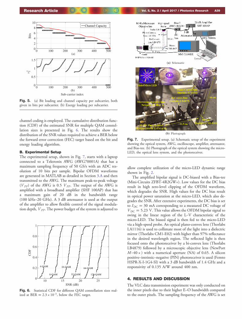
B. Experimental SetupThe experimental setup, shown in Fig. 7, starts with a laptopconnected to a Tektronix AWG (AWG70001A) that has amaximum sampling frequency of 50 GS/s with an ADC res-olution of 10 bits per sample. Bipolar OFDM waveformsare generated in MATLAB as detailed in Section 3.A and thentransmitted to the AWG. The maximum peak-to-peak voltage(V PP) of the AWG is 0.5 V PP . The output of the AWG isamplified with a broadband amplifier (SHF 100AP) that hasa maximum gain of 20 dB in the bandwidth range(100 kHz–20 GHz). A 3 dB attenuator is used at the outputof the amplifier to allow flexible control of the signal modula-tion depth, V PP . The power budget of the system is adjusted to
allow complete utilization of the micro-LED dynamic rangeshown in Fig. 2.
The amplified bipolar signal is DC-biased with a Bias-tee(Mini-Circuits ZFBT-4R2GW+). Low values for the DC biasresult in high zero-level clipping of the OFDM waveform,which degrades the SNR. High values for the DC bias resultin optical power saturation at the micro-LED, which also de-grades the SNR. After extensive experiments, the DC bias is setto IDC � 30 mA corresponding to a measured DC voltage ofV DC � 5.23 V. This value allows the OFDM bipolar signal toswing in the linear region of the L–V characteristic of themicro-LED. The biased signal is then fed to the micro-LEDvia a high-speed probe. An optical plano-convex lens (ThorlabsLA1116) is used to collimate most of the light into a dielectricmirror (Thorlabs CM1-E02) with higher than 97% reflectancein the desired wavelength region. The reflected light is thenfocused onto the photoreceiver by a bi-convex lens (ThorlabsLB4879) followed by a microscopic objective lens (NewPortM–40 × ) with a numerical aperture (NA) of 0.65. A siliconpositive–intrinsic–negative (PIN) photoreceiver is used (FemtoHSPR-X-I-1G4-SI) with a 3 dB bandwidth of 1.4 GHz and aresponsivity of 0.135 A/W around 400 nm.
4. RESULTS AND DISCUSSION
The VLC data transmission experiment was only conducted onthe inner pixels due to their higher E–O bandwidth comparedto the outer pixels. The sampling frequency of the AWG is set
(a)0 100 200 300 400 500
0 100 200 300 400 500
Bits
0
2
4
6
8
10Channel Capacity
(b) Sub-carrier index
0
0.5
1
1.5
Fig. 5. (a) Bit loading and channel capacity per subcarrier, bothgiven in bits per subcarrier. (b) Energy loading per subcarrier.
10 15 20 25SNR (dB)
0
0.2
0.4
0.6
0.8
1
CD
F
128-QAM32-QAM8-QAM
64-QAM16-QAM4-QAM
Fig. 6. Statistical CDF for different QAM constellation sizes real-ized at BER � 2.3 × 10⁻³, below the FEC target.
20 dB AmplifierSHF 100AP
3 dB Attenuator
(a)
16 cm
11.5 cm
Microscope objective lensNewport (M-40x)
SI-PIN PhotoreceiverFEMTO (HSPR-X-I-1G4-SI)
Violet Micro LED
Bi-Convex lensThorlabs (LB4879)
Plano-Convex lensThorlabs (LA1116)
MirrorThorlabs (CM1-E02)
(b)
Fig. 7. Experimental setup. (a) Schematic setup of the experimentshowing the optical system, AWG, oscilloscope, amplifier, attenuator,and Bias-tee. (b) Photograph of the optical system showing the micro-LED, the optical lens system, and the photoreceiver.
Research Article Vol. 5, No. 2 / April 2017 / Photonics Research A39
to 29 GS/s with an oversampling factor of eight samples persymbol, which results in a single-sided modulation bandwidthof 1.81 GHz. The subcarriers are equally spaced within theNyquist rate of the modulation signal with a subcarrier spacingof 3.54 MHz. The high-speed equipment used in the measure-ments allowed for the overall system bandwidth to be limitedby the bandwidth of the micro-LED. Figure 8 shows the datarates, and the corresponding theoretical lower bounds and ex-perimentally obtained values for the BERs at different dimminglevels. The theoretical lower bounds for the BER estimationsare calculated based on the experimentally estimated SNR asdescribed in Eq. (5), and they are shown to be close to theexperimental results. The data rates start with 3.46 Gb/s at areceived optical power, Popt � −4.94 dBm, which correspondsto a DC bias of V DC � 4.16 V and a DC current ofIDC � 10 mA. The data rate increases, but starts to saturateas the DC bias increases until it reaches a maximum of4.91 Gb/s at Popt � −2.29 dBm corresponding to V DC �5.21 V and IDC � 35 mA. The data rate starts to decreaseas the DC bias increases beyond 35 mA. This result is expecteddue to the increased clipping distortion caused by the opticalpower saturation shown in Fig. 2. The achieved BER for all thestudied cases in this test is well below the 3.8 × 10⁻³ FECthreshold. The optimized DC bias was selected for the restof the measurements as V DC � 5.11 V and IDC �30 mA, since the system performance for a larger swing of thepeak-to-peak modulation signal starts to degrade at IDC �35 mA. The theoretical lower bounds of the BER versus datarates at different dimming levels are shown in Fig. 9 with acomparison to the experimental results. The deviationbetween theoretical and experimental validation points atPopt � −4.94 dBm is due to the severe clipping distortion atDC current IDC � 10 mA.
The system performance as a function of the modulationsignal depth, V PP, is investigated. A large modulation signalswing is expected to increase the SNR due to the increased sig-nal power, σ2x . Nevertheless, it incurs additional nonlinear dis-tortion, σ2d , due to the increased clipping. It is shown in Fig. 10that the SNR improves as the modulation depth increases. Thenonlinear distortion is present on the first 250 MHz; however,
the improvement in the signal power σ2x is more significant athigher frequencies. This result is justified by the fact thatsignals at higher frequencies are attenuated due to the lowerchannel gain at these high frequencies. Therefore, these valuesbecome less affected by the nonlinearity of the device. Thisresult shows that tolerating additional nonlinearity byemploying a larger signal swing can improve the communica-tion system performance.
The experimentally optimized values for the DC bias at30 mA and the modulation signal swing at 3.88V PP are usedto investigate the system data rate performance against BER.The experimentally obtained data rates versus BERs are pre-sented with the theoretical lower bounds for the BER perfor-mance in Fig. 11. The theoretical lower bounds are shown to bevery close to the experimentally obtained results. As shown inFig. 11, a transmission data rate of 7.91 Gb/s is experimentallyachieved at a BER below the FEC threshold, 3.8 × 10⁻³. Toguarantee reliable communications, the data rate is reducedto 7.36 Gb/s to allow for a 7% FEC overhead to be employed.This compares to 5 Gb/s for a device with similar designemitting at 450 nm [7]. To the best of the authors’ knowledge,
Fig. 8. Experimentally obtained results and theoretical bounds ofdata rate and BER versus different dimming levels at a modulationdepth of V PP � 2.36 V. The values for the received optical powercorrespond to DC-bias values ranging from 10 to 40 mA.
Fig. 9. Theoretical bounds on the data rate versus BER for differentdimming levels at a modulation depth of V PP � 2.36 V. The valuesfor the received optical power correspond to DC-bias values rangingfrom 10 to 40 mA. Filled markers denote experimental results.
Fig. 10. SNR versus frequency for different modulation depths atDC-bias current IDC � 30 mA. The values for the modulation signalswings correspond to feeding the micro-LED with varying power levelsfrom 5.85 to 11.78 dBm.
A40 Vol. 5, No. 2 / April 2017 / Photonics Research Research Article
this record is the highest for VLCs data transmission speedsusing single micro-LED.
The system data rate performance is investigated when thewaveform averaging acquisition mode of the oscilloscope isactivated. Averaging acquisition was shown to be useful indrawing conclusions from experimental studies that could in-fluence practical system design [23]. The averaging acquisitionmode in this experiment allows for a better characterization ofthe micro-LED by reducing the AWGN of the photoreceiver,which limits the system performance to the nonlinear distor-tion noise of the micro-LED. It is shown in Fig. 11 that datarates up to 11.95 Gb/s can be achieved at a BER below the FECthreshold. This is reduced to 11.12 Gb/s when 7% FEC over-head is used. The results for the waveform acquisition modeof the oscilloscope are only presented to show the effect ofthe nonlinear distortion in the absence of the photoreceiverAWGN noise. All other reported results were conducted with-out waveform averaging acquisition.
5. RANGE AND ALIGNMENT CONSIDERATIONS
The VLC system was realized using an optical system to collect,collimate, and focus the light on the PD. The used optical sys-tem imposes restrictions on the link alignment and transmis-sion range. Introducing optimized optics and deploying moremicro-LED pixels from the array can improve both the cover-age and the range of the system. The feasibility of demonstrat-ing long transmission distances was demonstrated at a free-space distance of 10 m and a data rate of 1.1 Gb/s inRef. [24]. This was achieved using an avalanche photodiode(APD) with an integrated concentrator, and a micro-LED withan optical power of 4.5 mW, which is 1.96 times higher thanthe optical power of the micro-LED pixel used in this work.
The obtained data rates and BERs for different received op-tical power presented in Fig. 8 enable us to investigate the sys-tem performance against the transmission range based on thewidely accepted line-of-sight (LoS) optical wireless communi-cation (OWC) propagation models [25]. The methodology isto compute the distances which result in the respective receivedoptical power presented in Fig. 8 and the distances are then
cross-mapped with the data rates achieved in Fig. 8. Note thatthe results shown in Fig. 8 are obtained at different dimminglevels by varying the DC-bias point, which limits the operatingbandwidth and the experimentally obtained data rates. Ananalysis of the system range is provided based on four studies:(I) with transmitter and receiver lenses, (II) with transmitterlens only, (III) with receiver lens only, and (IV) without anyoptics. In all cases we assume that all array pixels are used(15 micro-LEDs) in a ganging OFDMmode. This can increasethe mutual heat between the pixels and consequently degradethe total aggregate data rates; therefore the results in this sectioncan be considered as upper bounds on the system performance.
The LoS channel gain can be given as [25]
H �0� � �m� 1�A2πd 2 cosm�ϕ�T �ψ�g�ψ� cos�ψ�; (7)
where m � −1∕log2�cos�Φ1∕2�� is the Lambertian order of theoptical source and Φ1∕2 denotes its semi-angle; ϕ is the angleof irradiance; A is the detection area of the APD; d is theEuclidean distance between the optical source and the APD;ψ is the angle of incidence; T �ψ� represents the gain of theoptical filter used at the receiver; and g�ψ� represents the gainof the optical concentrator, given as [25]
g�ψ� ��
n2sin2�Ψfov� ; 0 ≤ ψ ≤ Ψfov
0; ψ > Ψfov
; (8)
where n is the refractive index of the optical concentrator usedat the APD. The optical power after the transmitter lens can begiven as [26]
PR;lensopt � �mLED � 1�D2
lens
8d 02 T lensPT ;LEDopt ; (9)
where mLED denotes the Lambertian order of the micro-LED,Dlens is the lens diameter, T lens is the transmittance of the lens,and d 0 is the distance between the micro-LED and the trans-mitter lens. The existence of the transmitter lens affects themicro-LED beam divergence. The half power semi-angle Φlens
1∕2can be given as [26]
Φlens1∕2 �
Ds
2d 0 ; (10)
where Ds is the diameter of the micro-LED. The transmitterlens used in this investigation is an aspheric condenser lens(Thorlabs ACL7560U-A) with a diameter of Dlens � 75 mm,and a focal length of lens f � 60 mm.
A commercially available compound parabolic concentrator(CPC) is assumed to be in front of the APD. The field-of-view(FOV) of the concentrator is 25°, with a refractive index ofn � 1.5. We assume the use of a high-speed commerciallyavailable APD at the receiver (Thorlabs APD210) instead ofthe used PIN receiver (Femto HSPR-X-I-1G4-SI). The APDdiameter is 0.5 mm, and the modulation bandwidth is1.6 GHz. The APD improves the sensitivity of the receiver;therefore an APD conversion gain factor is introduced toallow a fair comparison between the experimentally obatinedresults using the PIN and the numerical results using theAPD photoreceivers:
ΛAPD � GAPD
GPIN; (11)
Fig. 11. Data rates versus BER for the experimentally obtainedand the theoretical bounds at DC-bias current IDC � 30 mA corre-sponding to Popt � −2.6 dBm and modulation depth V PP � 3.88 V.
Research Article Vol. 5, No. 2 / April 2017 / Photonics Research A41
where GAPD and GPIN are the conversion gains of the APDand PIN photoreceivers given in V/W, respectively. UsingEqs. (7)–(11), the received optical power at the APD can begiven as
PRx;APDopt � �mlens � 1�A
2πd 2 cosmlens�ϕ�
× T �ψ�g�ψ� cos�ψ�ΛAPDPR;lensopt ; (12)
where mlens is the Lambertian order of the lens basedon Eq. (10).
The LoS propagation model is used to compute the trans-mission ranges that can achieve certain values for the receivedoptical power between −5 and −2 dBm. These values for thereceived optical power were demonstrated experimentally toachieve data rates between 3.46 and 4.91 Gb/s using the ex-perimentally realized VLC system. An upper bound on the datarates can be estimated by cross-mapping the computed receivedpower at each distance, with the experimentally obtained datarates provided in Fig. 8. The distance versus received opticalpower and data rate for Studies I and II and Studies III andIV is shown in Fig. 12, respectively. The largest distancescan be achieved using transmitter and receiver optics.
Specifically, it was found that at 3.69 m distance a data rateof 4.91 Gb/s can be achieved, and at 5.25 m distance the datarate reduces to 3.46 Gb/s. As expected, the transmitter lens isshown to boost the range more than the receiver concentratorlens. At a data rate of 4.91 Gb/s, the maximum distance is1.04 m and 4.7 cm for Studies II and III, respectively. At adata rate of 3.46 Gb/s, the maximum distance is 1.47 mand 6.6 cm for Studies II and III, respectively. The transmissionranges that can be supported at data rates above 3.46 Gb/s areless than 2 cm when optics are not used.
The received optical power distribution is investigated as afunction of the receiver’s vertical–horizontal misalignments forthe four considered studies, as shown in Fig. 13. The resultsare presented for the received optical power values that allow amaximum of −2 dBm and a minimum of −5 dBm, correspond-ing to data rates of 4.91 and 3.46 Gb/s, respectively. The trans-mission range and the system robustness against misalignments areboth improved when optics are used for both front-end compo-nents in Study I, which makes this scenario suitable for high-speedpoint-to-point applications. The transmitter lens in Study II im-proves the transmission range but reduces the system robustnessagainst misalignments. The receiver lens in Study III reduces theperformance degradation caused by misalignment at the expenseof reducing the system range. The transmission range and the sys-tem robustness against misalignments are both degraded in StudyIV. However, Studies III and IV are suitable for board-to-boardcommunication links, where wired links are not possible becauseof the rotational requirements between the boards for example.
6. CONCLUSION
A novel violet micro-LED array with two sets of inner andouter pixels is reported in this paper. The inner pixels allowvery high current densities due to the small active area, enablingE–O bandwidth up to 655 MHz at an optical output power of2.3 mW. An OFDM-based VLC system using a single pixel of
(a) (b)
Fig. 12. Distance versus received optical power (left) and data rate(right). (a) Study I with transmitter and receiver lenses and Study IIwith transmitter lens only. (b) Study III with receiver lens only andStudy IV without any optics.
-2.1
5
-2.15
-2.15
-2.1
5
-2.1
-2.1
-2.1
-2.1
-2.1
-2.05
-2.05-2.05
-2.05
-2-2
-5 0 5X (mm)
(a)
-5
0
5
Y (
mm
)
-2.25
-2.2
-2.15
-2.1
-2.05
-2
-4
-4
-4
-4
-3.5
-3.5
-3.5-3.5
-3.5
-3.5
-3
-3
-3
-3
-3
-2.5
-2.5
-2.5
-2
-5 0 5X (mm)
-5
0
5
Y (
mm
)
-5
-4
-3
-2
-2.2-2.2
-2.2-2
.2
-2.18-2.18
-2.18
-2.18
-2.1
6
-2.16
-2.16
-2.1
6
-2.14
-2.14
-2.14
-2.1
4
-2.14 -2.12
-2.12
-2.12
-2.1
2
-2.12
-2.1
-2.1-2.1
-2.1
-2.08
-2.08
-2.08
-2.0
6
-5 0 5X (mm)
-5
0
5
Y (
mm
)
-2.25
-2.2
-2.15
-2.1
-3.6-3.6
-3.6-3
.6
-3.4
-3.4
-3.4
-3.4
-3.2
-3.2
-3.2
-3.2
-3
-3
-3-3
-3
-3
-2.8
-2.8
-2.8
-2.8
-2.8-2.6
6.2-
-2.6
-2.6
-2.4
-2.4-2.4
-2.4
-2.2
-2.2
-2.2
-2
-2
-5 0 5X (mm)
-5
0
5
Y (
mm
)
-4
-3.5
-3
-2.5
-2(g)(c)
-5.14-5.14
-5.14
-5.14
-5.12
-5.1
2
-5.12-5.12
-5.12
-5.12
-5.1
-5.1
-5.1
-5.1
-5.1-5.08
-5.08-5.08
-5.08
-5.06
-5.06
-5 0 5X (mm)
-5
0
5
Y (
mm
)
-5.18
-5.16
-5.14
-5.12
-5.1
-5.08
(b)
-6.2-6.2
-6.2-6
.2
-6
-6
-6
-6
-5.8
-5.8
-5.8-5.8
-5.8
-5.8
-5.6
-5.6
-5.6
-5.6
-5.6
-5.4
-5.4
-5.4
-5.4
-5.2
-5.2
-5.2
-5 0 5X (mm)
-5
0
5
Y (
mm
)
-6.5
-6
-5.5
-5.07-5.07
-5.07
-5.07
-5.0
6
-5.06
-5.06
-5.0
6
-5.05
-5.0
5
-5.05-5.05
-5.05
-5.04
-5.04
-5.04
-5.0
4
-5.04
-5.03
-5.03
-5.03
-5.03
-5.0
2
-5.02
-5.02
-5.0
1
-5.01
-5 0 5X (mm)
-5
0
5
Y (
mm
)
-5.1
-5.08
-5.06
-5.04
-5.02
-6-6
-6
-6
-5.9
-5.9
-5.9
-5.9
-5.8
-5.8
-5.8
-5.8
-5.7
-5.7
-5.7-5.7
-5.7
-5.6
-5.6
-5.6
-5.6
-5.6
-5.5
-5.5
-5.5
-5.5-5.4
-5.4
-5.4
-5.3
-5.3
-5.3
-5.2
-5 0 5X (mm)
-5
0
5
Y (
mm
)
-6.2
-6
-5.8
-5.6
-5.4
-5.2(d)
(e)
(f) (h)
Fig. 13. Received optical power distribution in dBm as a function of vertical–horizontal displacements. (a) Study I at a distance of 369 cm;(b) Study I at a distance of 525 cm; (c) Study II at a distance of 104 cm; (d) Study II at a distance of 147 cm; (e) Study III at a distance of 4.7 cm;(f ) Study III at a distance of 6.6 cm; (g) Study IV at a distance of 1.3 cm; (h) Study IV at a distance of 1.9 cm.
A42 Vol. 5, No. 2 / April 2017 / Photonics Research Research Article
the proposed violet micro-LED is realized using adaptive bit andenergy loading. The nonlinear distortion is found to affect theslow frequency region of the overall system bandwidth due tothe limited dynamic range of the micro-LED. A transmission rateof 11.12 Gb/s, including the 7% FEC overhead, is achieved byaveraging out thermal and shot noise of the photoreceiver andlimiting the overall VLC system noise to the nonlinear distortionof the micro-LED. This result represents an upper bound on theproposed micro-LED performance that can be approached whenhigher quality system components with lower noise margins areused. A data transmission rate of 7.36 Gb/s, including the 7%FEC overhead, is also reported when all the noise sources ofthe VLC system are considered. The theoretical bounds are ingood approximation with the experiment results.
The numerical investigation of the range and alignmenthighlights the role of optimized optics in increasing the trans-mission distance and improving system robustness.
Funding. Engineering and Physical Sciences ResearchCouncil (EPSRC) (EP/K00042X/1, EP/M506515/1).
†These authors contributed equally to this work.
REFERENCES1. Cisco Visual Networking Index, “The zettabyte era: trends and
analysis,” Cisco White Paper, 2015, http://www.cisco.com/c/en/us/solutions/collateral/service‑provider/visual‑networking‑index‑vni/VNI_Hyperconnectivity_WP.pdf.
2. Y. Zhou, J. Zhao, M. Zhang, J. Shi, and N. Chi, “2.32 Gbit/s phospho-rescent white LED visible light communication aided by two-stagedlinear software equalizer,” in 10th International Symposium onCommunication Systems, Networks and Digital Signal Processing(CSNDSP) (IEEE, 2016), pp. 1–4.
3. J. Herrnsdorf, J. J. D. McKendry, E. Xie, M. J. Strain, E. Gu, I. M.Watson, and M. D. Dawson, “Gallium nitride structured illuminationlight sources,” in Light, Energy and the Environment Conference(Optical Society of America, 2016), paper SSM2C.1.
4. J. J. D. McKendry, R. P. Green, A. E. Kelly, Z. Gong, B. Guilhabert,D. Massoubre, E. Gu, and M. D. Dawson, “High-speed visible lightcommunications using individual pixels in a micro light-emitting diodearray,” IEEE Photon. Technol. Lett. 22, 1346–1348 (2010).
5. P. P. Maaskant, H. Shams, M. Akhter, W. Henry, M. J. Kappers, D.Zhu, C. J. Humphreys, and B. Corbett, “High-speed substrate-emittingmicro-light-emitting diodes for applications requiring high radiance,”Appl. Phys. Express 6, 022102 (2013).
6. D. Tsonev, H. Chun, S. Rajbhandari, J. J. D. McKendry, S. Videv, E.Gu, M. Haji, S. Watson, A. E. Kelly, G. Faulkner, M. D. Dawson, H.Haas, and D. O’Brien, “A 3-Gb/s single-LED OFDM-based wirelessVLC link using a gallium nitride μLED,” IEEE Photon. Technol. Lett.26, 637–640 (2014).
7. R. Ferreira, E. Xie, J. McKendry, S. Rajbhandari, H. Chun, G.Faulkner, S. Watson, A. E. Kelly, E. Gu, R. Penty, I. White, D.O’Brien, and M. D. Dawson, “High bandwidth GaN-based micro-LEDs for multi-Gbps visible light communications,” IEEE Photon.Technol. Lett. 28, 2023–2026 (2016).
8. C. J. Humphreys, “Solid-state lighting,” MRS Bull. 33(4), 459–470(2008).
9. A. Zukauskas, R. Vaicekauskas, and M. S. Shur, “Colour-renditionproperties of solid-state lamps,” J. Appl. Phys. D 43, 354006(2010).
10. J. M. Phillips, M. E. Coltrin, M. H. Crawford, A. J. Fischer, M. R.Krames, R. Mueller-Mach, G. O. Mueller, Y. Ohno, L. E. S.Rohwer, J. A. Simmons, and J. Y. Tsao, “Research challenges toultra-efficient inorganic solid-state lighting,” Laser Photon. Rev. 1,307–333 (2007).
11. Q. Dai, Q. Shan, H. Lam, L. Hao, Y. Lin, and Z. Cui, “Circadian-effectengineering of solid-state lighting spectra for beneficial and tunablelighting,” Opt. Express 24, 20049–20058 (2016).
12. Z. Gong, Y. F. Zhang, P. Kelm, I. M. Watson, E. Gu, and M. D.Dawson, “InGaN micro-pixellated light-emitting diodes with nano-textured surfaces and modified emission profiles,” Appl. Phys. A103, 389–393 (2011).
13. D. J. F. Barros, S. K. Wilson, and J. M. Kahn, “Comparison of orthogo-nal frequency-division multiplexing and pulse-amplitude modulation inindoor optical wireless links,” IEEE Trans. Commun. 60, 153–163(2012).
14. J. McKendry, D. Tsonev, R. Ferreira, S. Videv, A. Griffiths, S. Watson,E. Gu, A. Kelly, H. Haas, and M. Dawson, “Gb/s single-LEDOFDM-based VLC using violet and UV gallium nitride μLEDs,” inIEEE Summer Topicals Meeting Series (SUM) (IEEE, 2015),paper TuD4.3.
15. M. S. Islim and H. Haas, “Modulation techniques for Li-Fi,” ZTECommun. 14, 29–40 (2016).
16. D. Tsonev, S. Sinanovic, and H. Haas, “Complete modelling ofnonlinear distortion in OFDM-based optical wireless communication,”J. Lightwave Technol. 31, 3064–3076 (2013).
17. D. Tsonev, S. Videv, and H. Haas, “Unlocking spectral efficiency inintensity modulation and direct detection systems,” IEEE J. Sel. AreasCommun. 33, 1758–1770 (2015).
18. P. Banelli and S. Cacopardi, “Theoretical analysis and performance ofOFDM signals in nonlinear AWGN channels,” IEEE Trans. Commun.48, 430–441 (2000).
19. S. Dimitrov and H. Haas, “Information rate of OFDM-based opticalwireless communication systemswith nonlinear distortion,” J. LightwaveTechnol. 31, 918–929 (2013).
20. H. E. Levin, “A complete and optimal data allocation method forpractical discrete multitone systems,” in Proceedings of IEEE GlobalTelecommunications Conference (IEEE, 2001), pp. 369–374.
21. F. Xiong, Digital Modulation Techniques, 2nd ed. (Artech House,2006).
22. C. E. Shannon, “A mathematical theory of communication,” Bell Syst.Tech. J. 27, 379–423 (1948).
23. L. Peng, S. Haese, and M. Hèlard, “Optimized discrete multitonecommunication over polymer optical fiber,” J. Opt. Commun. Netw.5, 1313–1327 (2013).
24. J. Jiang, Y. Huo, F. Jin, P. Zhang, Z. Wang, Z. Xu, H. Haas, and L.Hanzo, “Video streaming in the multiuser indoor visible light downlink,”IEEE Access 3, 2959–2986 (2015).
25. J. M. Kahn and J. R. Barry, “Wireless infrared communications,” Proc.IEEE 85, 265–298 (1997).
26. J. Fakidis, M. Ijaz, S. Kucera, H. Claussen, and H. Haas, “On the de-sign of an optical wireless link for small cell backhaul communicationand energy harvesting,” in IEEE International Symposium on Personal,Indoor and Mobile Radio Communications (PIMRC) (IEEE, 2014),pp. 58–62.
Research Article Vol. 5, No. 2 / April 2017 / Photonics Research A43