An IMPORTANT NOTICE at the end of this data sheet addresses availability, warranty, changes, use in safety-critical applications,intellectual property matters and other important disclaimers. PRODUCTION DATA.
TPS40303, TPS40304, TPS40305SLUS964D –NOVEMBER 2009–REVISED MARCH 2018
TPS4030x 3-V to 20-V Input, Voltage Mode, Synchronous Buck Controller
1
1 Features1• Input Voltage Range From 3 V to 20 V• 300-kHz (TPS40303), 600-kHz (TPS40304), and
1.2-MHz (TPS40305) Switching Frequencies• High- and Low-Side FET RDS(on) Current Sensing• Programmable Thermally Compensated OCP
Levels• Programmable Soft Start• 600-mV, 1% Reference Voltage• Voltage Feed-Forward Compensation• Supports Prebiased Output• Frequency Spread Spectrum• Thermal Shutdown Protection at 145°C• 10-Pin 3-mm × 3-mm VSON Package With
Ground Connection to Thermal Pad• Create a Custom Design Using the TPS4030x
With the WEBENCH® Power Designer
2 Applications• POL Modules• Printers• Digital TVs• Telecom• USB Type-C Wall Receptacles
3 DescriptionThe TPS4030x is a family of cost-optimizedsynchronous buck controllers that operate from 3-V to20-V input. The controller implements a voltage-modecontrol architecture with input-voltage feed-forwardcompensation that responds instantly to a change ininput voltage. The switching frequency is fixed at300 kHz, 600 kHz, or 1.2 MHz.
The frequency spread-spectrum (FSS) feature addsto the switching frequency, significantly reducing thepeak EMI noise and making it much easier to complywith EMI standards.
The TPS4030x offers design with a variety of user-programmable functions, including soft start,overcurrent protection (OCP) levels, and loopcompensation.
OCP level may be programmed by a single externalresistor connected from the LDRV pin to circuitground. During initial power on, the TPS4030x entersa calibration cycle, measures the voltage at the LDRVpin, and sets an internal OCP voltage level. Duringoperation, the programmed OCP voltage level iscompared to the voltage drop across the low-sideFET when it is on to determine whether there is anovercurrent condition. The TPS4030x then enters ashutdown and restart cycle until the fault is removed.
Device Information(1)
PART NUMBER PACKAGE BODY SIZE (NOM)TPS40303
VSON (10) 3.00 mm × 3.00 mmTPS40304TPS40305
(1) For all available packages, see the orderable addendum atthe end of the data sheet.
9 Power Supply Recommendations ...................... 2910 Layout................................................................... 30
10.1 Layout Guidelines ................................................. 3010.2 Layout Example .................................................... 31
11 Device and Documentation Support ................. 3211.1 Device Support...................................................... 3211.2 Custom Design With WEBENCH® Tools ............. 3211.3 Documentation Support ........................................ 3211.4 Related Links ........................................................ 3211.5 Receiving Notification of Documentation Updates 3211.6 Community Resources.......................................... 3311.7 Trademarks ........................................................... 3311.8 Electrostatic Discharge Caution............................ 3311.9 Glossary ................................................................ 33
12 Mechanical, Packaging, and OrderableInformation ........................................................... 33
4 Revision HistoryNOTE: Page numbers for previous revisions may differ from page numbers in the current version.
Changes from Revision C (January 2018) to Revision D Page
• Changed title of data sheet for SEO ..................................................................................................................................... 1• Added "USB Type-C Wall Receptacles" to Applications; added links for WEBENCH........................................................... 1• Deleted redundant Dissipation Ratings table ........................................................................................................................ 4
Changes from Revision B (May 2015) to Revision C Page
• Added top nav icon for TPS40303 TI Design ........................................................................................................................ 1• Deleted Related Devices table from Device and Documentation Support .......................................................................... 32
Changes from Revision A (August 2012) to Revision B Page
• Added Pin Configuration and Functions section, ESD Ratings table, Feature Description section, Device FunctionalModes, Application and Implementation section, Power Supply Recommendations section, Layout section, Deviceand Documentation Support section, and Mechanical, Packaging, and Orderable Information section .............................. 1
Changes from Original (November 2009) to Revision A Page
• Changed minimum controllable pulse width max value from 100 to 70................................................................................. 5
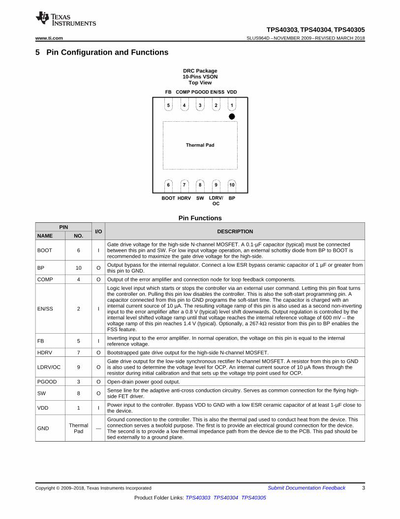
BOOT 6 IGate drive voltage for the high-side N-channel MOSFET. A 0.1-µF capacitor (typical) must be connectedbetween this pin and SW. For low input voltage operation, an external schottky diode from BP to BOOT isrecommended to maximize the gate drive voltage for the high-side.
BP 10 O Output bypass for the internal regulator. Connect a low ESR bypass ceramic capacitor of 1 µF or greater fromthis pin to GND.
COMP 4 O Output of the error amplifier and connection node for loop feedback components.
EN/SS 2 I
Logic level input which starts or stops the controller via an external user command. Letting this pin float turnsthe controller on. Pulling this pin low disables the controller. This is also the soft-start programming pin. Acapacitor connected from this pin to GND programs the soft-start time. The capacitor is charged with aninternal current source of 10 µA. The resulting voltage ramp of this pin is also used as a second non-invertinginput to the error amplifier after a 0.8 V (typical) level shift downwards. Output regulation is controlled by theinternal level shifted voltage ramp until that voltage reaches the internal reference voltage of 600 mV – thevoltage ramp of this pin reaches 1.4 V (typical). Optionally, a 267-kΩ resistor from this pin to BP enables theFSS feature.
FB 5 I Inverting input to the error amplifier. In normal operation, the voltage on this pin is equal to the internalreference voltage.
HDRV 7 O Bootstrapped gate drive output for the high-side N-channel MOSFET.
LDRV/OC 9 OGate drive output for the low-side synchronous rectifier N-channel MOSFET. A resistor from this pin to GNDis also used to determine the voltage level for OCP. An internal current source of 10 µA flows through theresistor during initial calibration and that sets up the voltage trip point used for OCP.
PGOOD 3 O Open-drain power good output.
SW 8 O Sense line for the adaptive anti-cross conduction circuitry. Serves as common connection for the flying high-side FET driver.
VDD 1 I Power input to the controller. Bypass VDD to GND with a low ESR ceramic capacitor of at least 1-µF close tothe device.
GND ThermalPad —
Ground connection to the controller. This is also the thermal pad used to conduct heat from the device. Thisconnection serves a twofold purpose. The first is to provide an electrical ground connection for the device.The second is to provide a low thermal impedance path from the device die to the PCB. This pad should betied externally to a ground plane.
(1) Stresses beyond those listed under Absolute Maximum Ratings may cause permanent damage to the device. These are stress ratingsonly and functional operation of the device at these or any other condition beyond those included under Recommended OperatingConditions is not implied. Exposure to absolute-maximum-rated conditions for extended periods of time may affect device reliability.
6 Specifications
6.1 Absolute Maximum Ratingsover operating free-air temperature range (unless otherwise noted) (1)
MIN MAX UNITVDD –0.3 22 VSW –3 27 VSW (< 100-ns pulse width, 10 µJ) –5 VBOOT –0.3 30 VHDRV –5 30 VBOOT-SW, HDRV-SW (differential from BOOT or HDRV to SW) –0.3 7 VCOMP, PGOOD, FB, BP, LDRV, EN/SS –0.3 7 VOperating junction temperature, TJ –40 145 °CStorage temperature, Tstg –55 150 °C
(1) JEDEC document JEP155 states that 500-V HBM allows safe manufacturing with a standard ESD control process.(2) JEDEC document JEP157 states that 250-V CDM allows safe manufacturing with a standard ESD control process.
6.2 ESD RatingsVALUE UNIT
V(ESD) Electrostatic dischargeHuman-body model (HBM), per ANSI/ESDA/JEDEC JS-001 (1) ±2000
VCharged-device model (CDM), per JEDEC specification JESD22-C101 (2) ±1500
6.3 Recommended Operating ConditionsMIN NOM MAX UNIT
VDD Input voltage 3 20 VTJ Operating junction temperature –40 125 °C
(1) For more information about traditional and new thermal metrics, see the Semiconductor and IC Package Thermal Metrics applicationreport.
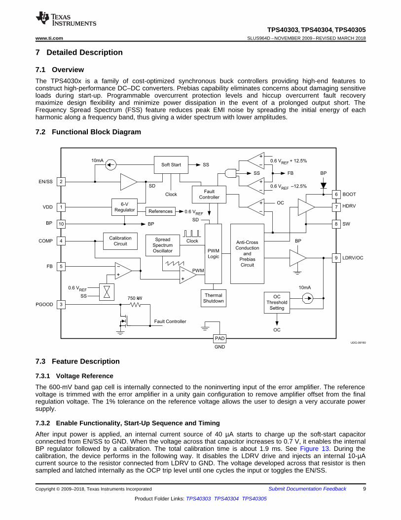
7.1 OverviewThe TPS4030x is a family of cost-optimized synchronous buck controllers providing high-end features toconstruct high-performance DC–DC converters. Prebias capability eliminates concerns about damaging sensitiveloads during start-up. Programmable overcurrent protection levels and hiccup overcurrent fault recoverymaximize design flexibility and minimize power dissipation in the event of a prolonged output short. TheFrequency Spread Spectrum (FSS) feature reduces peak EMI noise by spreading the initial energy of eachharmonic along a frequency band, thus giving a wider spectrum with lower amplitudes.
7.2 Functional Block Diagram
7.3 Feature Description
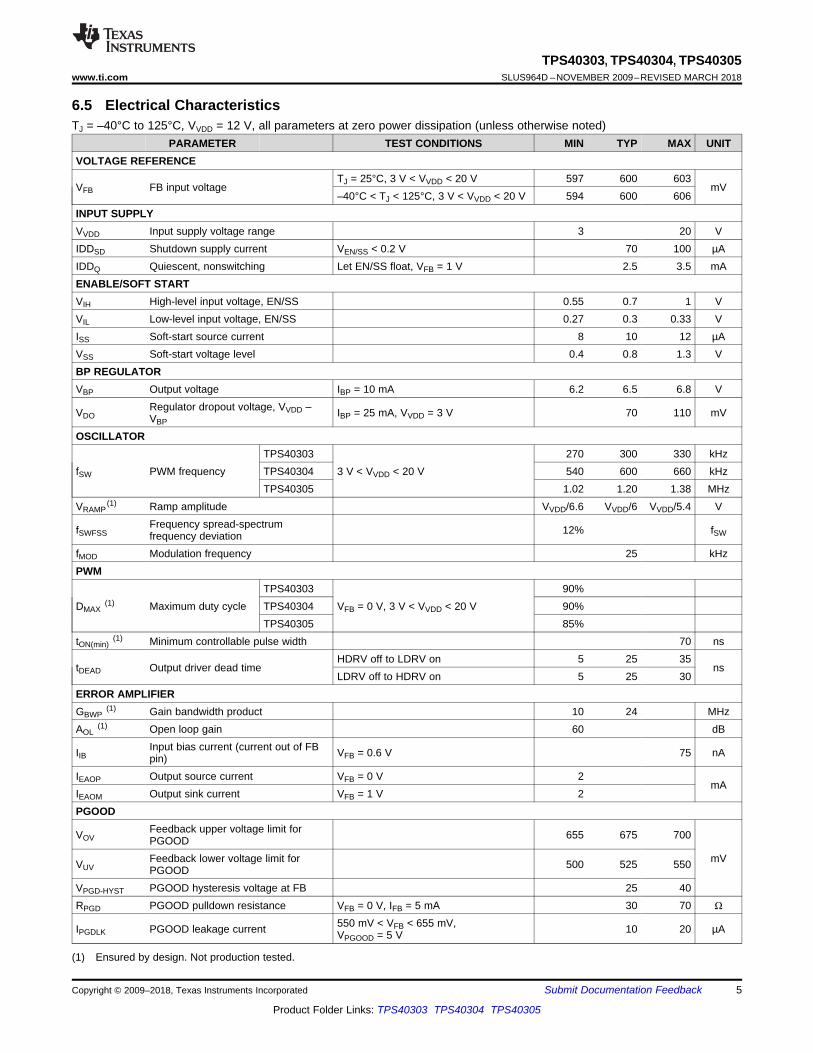
7.3.1 Voltage ReferenceThe 600-mV band gap cell is internally connected to the noninverting input of the error amplifier. The referencevoltage is trimmed with the error amplifier in a unity gain configuration to remove amplifier offset from the finalregulation voltage. The 1% tolerance on the reference voltage allows the user to design a very accurate powersupply.
7.3.2 Enable Functionality, Start-Up Sequence and TimingAfter input power is applied, an internal current source of 40 µA starts to charge up the soft-start capacitorconnected from EN/SS to GND. When the voltage across that capacitor increases to 0.7 V, it enables the internalBP regulator followed by a calibration. The total calibration time is about 1.9 ms. See Figure 13. During thecalibration, the device performs in the following way. It disables the LDRV drive and injects an internal 10-µAcurrent source to the resistor connected from LDRV to GND. The voltage developed across that resistor is thensampled and latched internally as the OCP trip level until one cycles the input or toggles the EN/SS.
The voltage at EN/SS is internally clamped to 1.3 V before and/or during calibration to minimize the dischargingtime once calibration. The discharging current is from an internal current source of 140 µA and it pulls the voltagedown to 0.4 V. The discharging current then initiates the soft-start by charging up the capacitor using an internalcurrent source of 10 µA. The resulting voltage ramp on this pin is used as a second noninverting input to theerror amplifier after an 800 mV (typical) downward level-shift; therefore, actual soft-start does not occur until thevoltage at this pin reaches 800 mV.
If EN/SS is left floating, the controller starts automatically. EN/SS must be pulled down to less than 270 mV toensure that the chip is in shutdown mode.
7.3.3 Soft-Start TimeThe soft-start time of the TPS4030x is user programmable by selecting a single capacitor. The EN/SS pinsources 10 µA to charge this capacitor. The actual output ramp-up time is the amount of time that it takes for the10 µA to charge the capacitor through a 600-mV range. There is some initial lag due to calibration and an offset(800 mV) from the actual EN/SS pin voltage to the voltage applied to the error amplifier.
The soft-start is done in a closed-loop fashion, meaning that the error amplifier controls the output voltage at alltimes during the soft-start period and the feedback loop is never open as occurs in duty cycle limit soft-startschemes. The error amplifier has two non-inverting inputs, one connected to the 600-mV reference voltage, andthe other connected to the offset EN/SS pin voltage. The lower of these two voltages is what the error amplifiercontrols the FB pin. As the voltage on the EN/SS pin ramps up past approximately 1.4 V (800-mV offset voltageplus the 600 mV reference voltage), the 600-mV reference voltage becomes the dominant input and theconverter has reached its final regulation voltage.
The capacitor required for a given soft-start ramp time for the output voltage is given by Equation 1.
where• CSS is the required capacitance on the EN/SS pin. (F)• ISS is the soft-start source current (10 µA).• VFB is the feedback reference voltage (0.6 V).• tSS is the desired soft-start ramp time (s). (1)
Feature Description (continued)7.3.4 Oscillator and Frequency Spread Spectrum (FSS)The oscillator frequency is internally fixed. The TPS40303 operating frequency is 300 kHz, the TPS40304operating frequency is 600 kHz, and the TPS40305 operating frequency is 1.2 MHz.
Connecting a resistor with a value of 267 kΩ ±10% from BP to EN/SS enables the FSS feature. When the FSS isenabled, it spreads the internal oscillator frequency over a minimum 12% window using a 25-kHz modulationfrequency with triangular profile. By modulating the switching frequency, side-bands are created. The emissionpower of the fundamental switching frequency and its harmonics is distributed into smaller pieces scatteredaround many sideband frequencies. The effect significantly reduces the peak EMI noise and makes it mucheasier for the resultant emission spectrum to pass EMI regulations.
7.3.5 Overcurrent ProtectionProgrammable OCP level at LDRV is from 6 mV to 150 mV at room temperature with 3000 ppm temperaturecoefficient to help compensate for changes in the low-side FET channel resistance as temperature increases.With a scale factor of 2, the actual trip point across the low-side FET is in the range of 12 mV to 300 mV. Theaccuracy of the internal current source is ±5%. Overall offset voltage, including the offset voltage of the internalcomparator and the amplifier for scale factor of 2, is limited to ±8 mV.
Maximum clamp voltage at LDRV is 340 mV to avoid turning on the low-side FET during calibration and in aprebiased condition. The maximum clamp voltage is fixed and it does not change with temperature. If the voltagedrop across ROCSET reaches the 340-mV maximum clamp voltage during calibration (no ROCSET resistorincluded), it disables OC protection. Once disabled, there is no low-side or high-side current sensing.
OCP level at HDRV is fixed at 450 mV with 3000-ppm temperature coefficient to help compensate for changes inthe high-side FET channel resistance as temperature increases. OCP at HDRV provides pulse-by-pulse currentlimiting.
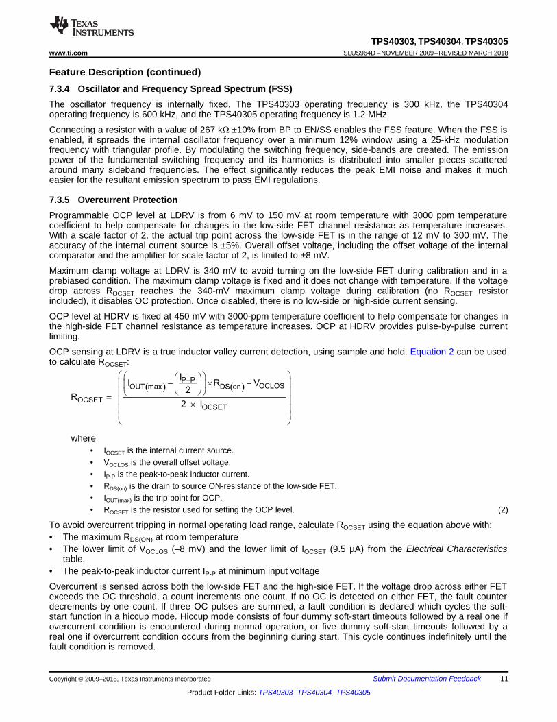
OCP sensing at LDRV is a true inductor valley current detection, using sample and hold. Equation 2 can be usedto calculate ROCSET:
where• IOCSET is the internal current source.• VOCLOS is the overall offset voltage.• IP-P is the peak-to-peak inductor current.• RDS(on) is the drain to source ON-resistance of the low-side FET.• IOUT(max) is the trip point for OCP.• ROCSET is the resistor used for setting the OCP level. (2)
To avoid overcurrent tripping in normal operating load range, calculate ROCSET using the equation above with:• The maximum RDS(ON) at room temperature• The lower limit of VOCLOS (–8 mV) and the lower limit of IOCSET (9.5 µA) from the Electrical Characteristics
table.• The peak-to-peak inductor current IP-P at minimum input voltage
Overcurrent is sensed across both the low-side FET and the high-side FET. If the voltage drop across either FETexceeds the OC threshold, a count increments one count. If no OC is detected on either FET, the fault counterdecrements by one count. If three OC pulses are summed, a fault condition is declared which cycles the soft-start function in a hiccup mode. Hiccup mode consists of four dummy soft-start timeouts followed by a real one ifovercurrent condition is encountered during normal operation, or five dummy soft-start timeouts followed by areal one if overcurrent condition occurs from the beginning during start. This cycle continues indefinitely until thefault condition is removed.
Feature Description (continued)7.3.6 DriversThe drivers for the external high-side and low-side MOSFETs can drive a gate-to-source voltage of VBP. TheLDRV driver for the low-side MOSFET switches between BP and GND, while the HDRV driver for the high-sideMOSFET is referenced to SW and switches between BOOT and SW. The drivers have nonoverlapping timingthat is governed by an adaptive delay circuit to minimize body diode conduction in the synchronous rectifier.
7.3.7 Prebias Start-UpThe TPS4030x contains a circuit to prevent current from being pulled from the output during start-up in thecondition the output is prebiased. There are no PWM pulses until the internal soft-start voltage rises above theerror amplifier input (FB pin), if the output is prebiased. Once the soft-start voltage exceeds the error amplifierinput, the controller slowly initiates synchronous rectification by starting the synchronous rectifier with a narrowon time. The controller then increments that on time on a cycle-by-cycle basis until it coincides with the timedictated by (1-D), where D is the duty cycle of the converter. This approach prevents the sinking of current froma prebiased output, and ensures the output voltage start-up and ramp to regulation is smooth and controlled.
7.3.8 Power GoodThe TPS4030x provides an indication that output is good for the converter. This is an open-drain signal and pullslow when any condition exists that would indicate that the output of the supply might be out of regulation. Theseconditions include the following:• VFB is more than ±12.5% from nominal.• Soft-start is active.• A short-circuit condition has been detected.
NOTEWhen there is no power to the device, PGOOD is not able to pull close to GND if anauxiliary supply is used for the power good indication. In this case, a built-in resistorconnected from drain to gate on the PGOOD pulldown device makes the PGOOD pin lookapproximately like a diode to GND.
7.3.9 Thermal ShutdownIf the junction temperature of the device reaches the thermal shutdown limit of 145°C, the PWM and the oscillatorare turned off and HDRV and LDRV are driven low. When the junction cools to the required level (125°C typical),the PWM initiates soft-start as during a normal power-up cycle.
7.4.1.1 UVLOIn UVLO, VDD is less than UVLO_ON, the BP6 regulator is off, and the HDRV and LDRV are held low byinternal passive discharge resistors.
7.4.1.2 DisableDisable is forced by holding SS/EN below 0.4 V. In disable, the BP6 regulator is off, and both HDRV and LDRVare held low by passive discharge resistors.
7.4.1.3 CalibrationEach enable of the TPS4030X3/4/5 devices requires a calibration which lasts approximately 2 ms. Duringcalibration the TPS40303/4/5 devices LDRV and HDRV are held off by their respective pulldown drivers while thedevice configures as detailed in Enable Functionality, Start-Up Sequence and Timing.
7.4.1.4 ConvertingWhen calibration completes, the TPS40303/4/5 devices ramp their reference voltage as described in Soft-StartTime, and the states of the LDRV and HDRV drivers are dictated by the COMP pin to regulate the FB pin equalto the internal reference.
NOTEInformation in the following applications sections is not part of the TI componentspecification, and TI does not warrant its accuracy or completeness. TI’s customers areresponsible for determining suitability of components for their purposes. Customers shouldvalidate and test their design implementation to confirm system functionality.
8.1 Application InformationThe TPS4030x is a family of cost-optimized synchronous buck controllers providing high-end features toconstruct high-performance DC-DC converters. Prebias capability eliminates concerns about damaging sensitiveloads during start-up. Programmable overcurrent protection levels and hiccup overcurrent fault recoverymaximize design flexibility and minimize power dissipation in the event of a prolonged output short. FrequencySpread Spectrum (FSS) feature reduces peak EMI noise by spreading the initial energy of each harmonic alonga frequency band, thus giving a wider spectrum with lower amplitudes.
8.2 Typical Applications
8.2.1 Using the TPS40305 for a 12-V to 1.8-V Point-of-Load Synchronous Buck RegulatorFigure 14 shows 12-V to 1.8-V at 10-A synchronous buck application using the TPS40305 switching at 1200 kHz.
Typical Applications (continued)8.2.1.1 Design RequirementsFor this example, follow the design parameters listed in Table 1.
Table 1. Design Example Electrical CharacteristicsPARAMETER TEST CONDITIONS MIN TYP MAX UNIT
VIN Input voltage 8 14 VVIN(ripple) Input ripple IOUT = 10 A 0.6 VVOUT Output voltage 0 A ≤ IOUT ≤ 10 A 1.764 1.800 1.836 V
Line regulation 8 V ≤ VIN ≤ 14 V 0.5%Load regulation 0 A ≤ IOUT ≤ 10 A 0.5%
VRIPPLE Output ripple IOUT = 10 A 36 mVVOVER Output overshoot IOUT falling from 7 A to 3 A 100 mVVUNDER Output undershoot IOUT rising from 3 A to 7 A 100 mVIOUT Output current 4.5 V ≤ VIN ≤ 5.5 V 0 10 AtSS Soft-start time VIN = 12 V 1.5 msISCP Short-circuit current trip point 13 15 AfSW Switching frequency 1200 kHz
Size 1 in2
The bill of materials for this application is shown in Table 2. The efficiency, line, and load regulation from boardsbuilt using this design are shown in Figure 14. Gerber files and additional application information are availablefrom the factory.
Table 2. Design Example List of MaterialsREFERENCEDESIGNATOR QTY VALUE DESCRIPTION SIZE PART NUMBER MFR
Click here to create a custom design using the TPS4030x devicse with the WEBENCH® Power Designer.1. Start by entering the input voltage (VIN), output voltage (VOUT), and output current (IOUT) requirements.2. Optimize the design for key parameters such as efficiency, footprint, and cost using the optimizer dial.3. Compare the generated design with other possible solutions from Texas Instruments.
The WEBENCH Power Designer provides a customized schematic along with a list of materials with real-timepricing and component availability.
In most cases, these actions are available:• Run electrical simulations to see important waveforms and circuit performance• Run thermal simulations to understand board thermal performance• Export customized schematic and layout into popular CAD formats• Print PDF reports for the design, and share the design with colleagues
Get more information about WEBENCH tools at www.ti.com/WEBENCH.
8.2.1.2.2 Selecting the Switching Frequency
To achieve the small size for this design, the TPS40305, with fSW = 1200 kHz, is selected for minimal externalcomponent size.
8.2.1.2.3 Inductor Selection (L1)
Synchronous buck power inductors are typically sized for approximately 30% peak-to-peak ripple current (IRIPPLE)
Given this target ripple current, the required inductor size can be calculated in Equation 3.
(3)
Selecting a standard 400-nH inductor value, solve for IRIPPLE = 3.5 A
The RMS current through the inductor is approximated by Equation 4.
(4)
8.2.1.2.4 Output Capacitor Selection (C12)
The selection of the output capacitor is typically driven by the output transient response. Equation 5 andEquation 6 overestimate the voltage deviation to account for delays in the loop bandwidth and can be used todetermine the required output capacitance.
(5)
(6)
If VIN(min) > 2 × VOUT, use overshoot (Equation 5) to calculate minimum output capacitance. If VIN(min) < 2 × VOUT,use undershoot (Equation 6) to calculate minimum output capacitance.
(7)
With a minimum capacitance, the maximum allowable ESR is determined by the maximum ripple voltage and isapproximated by Equation 8.
Two 0805, 22-µF, 6.3-V, X5R ceramic capacitors are selected to provide more than 35 µF of minimumcapacitance and less than 7 mΩ of ESR (2.5 mΩ each).
8.2.1.2.5 Peak Current Rating of Inductor
With output capacitance, it is possible to calculate the charge current during start-up and determine the minimumsaturation current rating for the inductor. The start-up charging current is approximated by Equation 9.
(9)
(10)
Table 3. Inductor RequirementsSYMBOL PARAMETER VALUE UNIT
L Inductance 400 nHIL(rms) RMS current (thermal rating) 10.05 AIL(peak) Peak current (saturation rating) 11.8 A
A PG0083.401, 400-nH inductor is selected for its small size, low DCR (3.0 mΩ) and high-current handlingcapability (17-A thermal, 27-A saturation).
8.2.1.2.6 Input Capacitor Selection (C8)
The input voltage ripple is divided between capacitance and ESR. For this design VRIPPLE(cap) = 150 mV andVRIPPLE(esr) = 150 mV. The minimum capacitance and maximum ESR are estimated by Equation 11.
(11)
(12)
The RMS current in the input capacitors is estimated by Equation 13.
(13)
Two 1210, 10-µF, 25-V, X5R ceramic capacitors with approximately 2-mΩ of ESR and a 2.5-A RMS currentrating each are selected. Higher voltage capacitors are selected to minimize capacitance loss at the DC biasvoltage to ensure the capacitors allow sufficient capacitance at the working voltage.
8.2.1.2.7 MOSFET Switch Selection (Q1 and Q2)
Reviewing available TI NexFET MOSFETs using TI’s NexFET MOSFET selection tool, the CSD16410Q5A andCSD16322Q5 5-mm × 6-mm MOSFETs are selected.
These two FETs have maximum total gate charges of 5 nC and 10 nC, respectively, which draws 18 mA at 1.2MHz from the BP regulator, less than its 50 mA minimum rating.
To ensure proper charging of the high-side FET gate, limit the ripple voltage on the boost capacitor to less than50 mV.
(14)
8.2.1.2.9 VDD Bypass Capacitor (C7)
Per the TPS40305 Electrical Characteristics specifications, select a 1.0-µF X5R or better ceramic bypasscapacitor for VDD.
8.2.1.2.10 BP Bypass Capacitor (C5)
As listed in the Electrical Characteristics, a minimum of 1.0-µF ceramic capacitance is required to stabilize theBP regulator. To limit regulator noise to less than 10 mV, the value of the bypass capacitor is calculated inEquation 15.
(15)
Because Q1 is larger than Q2, and the total gate charge of Q1 is 10 nC, a BP capacitor of 1.0 µF is calculated. Astandard value of 1.0 µF is selected to limit noise on the BP regulator.
8.2.1.2.11 Short-Circuit Protection (R11)
The TPS40305 uses the negative drop across the low-side FET at the end of the OFF time to measure theinductor current. Allowing for 30% over maximum load and 20% rise in RDS(on)Q1 for self-heating, the voltage dropacross the low-side FET at current limit is given by Equation 16.
(16)
The TPS40305 internal temperature coefficient helps compensate for the RDS(on) temperature coefficient of theMOSFET, so the current limit programming resistor is selected by Equation 17.
(17)
8.2.1.2.12 Feedback Divider (R4, R5)
The TPS40305 controller uses a full operational amplifier with an internally fixed 0.600-V reference. R4 isselected between 10 kΩ and 50 kΩ for a balance of feedback current and noise immunity. With R4 set to 10 kΩ,The output voltage is programmed with a resistor divider given by Equation 18.
(18)
8.2.1.2.13 Compensation: (C2, C3, C4, R3, R6)
Using the TPS40k Loop Stability Tool for 100-kHz bandwidth and 60° phase margin with a R4 value of 10.0 kΩ,the following values are returned.• C2 = C_1 = 820 pF• C3 = C_3 = 150 pF• C4 = C_2 = 3300 pF• R3 = R_2 = 422 Ω• R6 = R_3 = 2.20 kΩ
8.2.2 A High-Current, Low-Voltage Design Using the TPS40304For this 20-A, 12-V to 1.2-V design, the 600-kHz TPS40304 was selected for a balance between small size andhigh efficiency.
Figure 18. TPS40304 Design Example Schematic
8.2.2.1 Design RequirementsFor this example, follow the design parameters listed in Table 4.
Table 4. Design Example Electrical CharacteristicsPARAMETER TEST CONDITIONS MIN TYP MAX UNIT
VIN Input voltage 8 14 VVINripple Input ripple IOUT = 20 A 0.5 VVOUT Output voltage 0 A ≤ IOUT ≤ 20 A 1.164 1.200 1.236 V
Line regulation 8 V ≤ VIN ≤ 14 V 0.5%Load regulation 0 A ≤ IOUT ≤ 20 A 0.5%
VRIPPLE Output ripple IOUT = 20 A 36 mVVOVER Output overshoot 5 A ≤ IOUT ≤ 15 A 100 mVVUNDER Output undershoot 5 A ≤ IOUT ≤ 15 A 100 mVIOUT Output current 8 V ≤ VIN ≤ 14 V 0 20 AtSS Soft-start time VIN = 12 V 1.5 msISCP Short-circuit current trip point 26 AfSW Switching frequency 600 kHz
Size 1.5 in2
8.2.2.2 Detailed Design Procedure
8.2.2.2.1 Selecting the Switching Frequency
To achieve the small size for this design the TPS40304, with fSW = 600 kHz, is selected for minimal externalcomponent size.
8.2.2.2.2 Inductor Selection (L1)
Synchronous buck power inductors are typically sized for approximately 30% peak-to-peak ripple current (IRIPPLE)
Given this target ripple current, the required inductor size can be calculated in Equation 19.
(19)
Selecting a standard 300-nH inductor value, solve for IRIPPLE = 6 A
The RMS current through the inductor is approximated by Equation 20.
(20)
8.2.2.2.3 Output Capacitor Selection (C12)
The selection of the output capacitor is typically driven by the output transient response. Equation 21 andEquation 22 overestimate the voltage deviation to account for delays in the loop bandwidth and can be used todetermine the required output capacitance.
(21)
(22)
If VIN(min) > 2 × VOUT, use overshoot (Equation 21) to calculate minimum output capacitance. If VIN(min) < 2 × VOUT,use undershoot (Equation 22) to calculate minimum output capacitance.
(23)
With a minimum capacitance, the maximum allowable ESR is determined by the maximum ripple voltage and isapproximated by Equation 24.
(24)
Two 47-µF and one 220-µF capacitors are selected to provide more than 250 µF of minimum capacitance and5.2 mΩ of ESR.
8.2.2.2.4 Peak Current Rating of Inductor
With output capacitance, it is possible to calculate the charge current during start-up and determine the minimumsaturation current rating for the inductor. The start-up charging current is approximated by Equation 25.
(25)
(26)
Table 5. Inductor RequirementsPARAMETER VALUE UNIT
L Inductance 300 nHIL(rms) RMS current (thermal rating) 20.07 AIL(peak) Peak current (saturation rating) 23.25 A
The input voltage ripple is divided between capacitance and ESR. For this design VRIPPLE(cap) = 150 mV andVRIPPLE(esr) = 150 mV. The minimum capacitance and maximum ESR are estimated by Equation 27.
(27)
(28)
The RMS current in the input capacitors is estimated by Equation 29.
(29)
Three 1210, 10-µF, 25-V, X5R ceramic capacitors are selected. Higher voltage capacitors are selected tominimize capacitance loss at the DC bias voltage to ensure the capacitors allow sufficient capacitance at theworking voltage.
8.2.2.2.6 MOSFET Switch Selection (Q1 and Q2)
Reviewing available TI NexFET MOSFETs using the TI NexFET MOSFET selection tool, the CSD16410Q5A andCSD16321Q5 5-mm × 6-mm MOSFETs are selected.
These two FETs have maximum total gate charges of 5 nC and 10 nC, respectively.
8.2.2.2.7 Bootstrap Capacitor (C6)
To ensure proper charging of the high-side FET gate, limit the ripple voltage on the boost capacitor to less than50 mV.
(30)
8.2.2.2.8 VDD Bypass Capacitor (C7)
Per the TPS40304 data sheet, select a 1.0-uF X5R or better ceramic bypass capacitor for VDD.
8.2.2.2.9 BP Bypass Capacitor (C5)
Per the TPS40304 data sheet, a minimum 1.0-uF ceramic capacitance is required to stabilize the BP regulator.To limit regulator noise to less than 10 mV, the value of the bypass capacitor is calculated in Equation 31.
(31)
Because Q2 is larger than Q1, and the total gate charge of Q2 is 10 nC, a BP capacitor of 1.0 µF is calculated. Astandard value of 1.0 µF is selected to limit noise on the BP regulator.
8.2.2.2.10 Short-Circuit Protection (R11)
The TPS40304 uses the negative drop across the low-side FET at the end of the OFF time to measure theinductor current. Allowing for 30% over maximum load and 20% rise in RDS(on)Q1 for self-heating, the voltage dropacross the low-side FET at current limit is given by Equation 32.
(32)
The TPS40304 internal temperature coefficient helps compensate for the MOSFET RDS(on) temperaturecoefficient, so the current limit programming resistor is selected by Equation 33.
The TPS40304 controller uses a full operational amplifier with an internally fixed 0.6-V reference. R4 is selectedbetween 10 kΩ and 50 kΩ for a balance of feedback current and noise immunity. With R4 set to 10 kΩ, Theoutput voltage is programmed with a resistor divider given by Equation 34.
(34)
8.2.2.2.12 Compensation: (C2, C3, C4, R3, R6)
Using the TPS40k Loop Stability Tool for 100-kHz bandwidth and 60° phase margin with a R4 value of 10.0 kΩ,the following values are returned.• C4 = 680 pF• C5 = 100 pF• C6 = 680 pF• R1 = 10 kΩ• R2 = 1.5 kΩ
8.2.3 A Synchronous Buck Application Using the TPS40303Figure 22 shows a 3.3-V/5-V/12-V to 0.6-V at 10-A synchronous buck application using the TPS40303 switchingat 300 kHz.
Figure 22. TPS40303 Design Example Schematic
8.2.3.1 Design RequirementsFor this example, follow the design parameters listed in Table 6.
Table 6. Design Example Electrical CharacteristicsPARAMETER TEST CONDITIONS MIN TYP MAX UNIT
VIN Input voltage 3.3 14 VVINripple Input ripple IOUT = 10 A 0.6 VVOUT Output voltage 0 A ≤IOUT ≤ 10 A 0.582 0.6 0.618 V
Line regulation 3 V ≤ VIN ≤14 V 0.5%Load regulation 0 A ≤IOUT ≤ 10 A 0.5%
VRIPPLE Output ripple IOUT = 10 A 12 mVVOVER Output overshoot 3 A ≤ IOUT ≤ 7 A 100 mVVUNDER Output undershoot 3 A ≤IOUT ≤ 7 A 100 mVIOUT Output current 3.3 V ≤ VIN ≤ 14 V 0 10 AtSS Soft-start time VIN = 12 V 1.5 msISCP Short-circuit current trip point 13 15 A
Efficiency VIN = 12 V, IOUT = 5 A 84%fSW Switching frequency 300 kHz
To achieve the small size for this design the TPS40303, with fSW = 300 kHz, is selected for minimal externalcomponent size.
8.2.3.2.2 Inductor Selection (L1)
Synchronous buck power inductors are typically sized for approximately 30% peak-to-peak ripple current (IRIPPLE)
Given this target ripple current, the required inductor size can be calculated in Equation 35.
(35)
Selecting a standard 600-nH inductor value, solve for IRIPPLE = 3.2 A
The RMS current through the inductor is approximated by Equation 36.
(36)
8.2.3.2.3 Output Capacitor Selection (C12)
The selection of the output capacitor is typically driven by the output transient response. Equation 37 andEquation 38 overestimate the voltage deviation to account for delays in the loop bandwidth and can be used todetermine the required output capacitance.
(37)
(38)
If VIN(min) > 2 × VOUT, use overshoot (Equation 37) to calculate minimum output capacitance. If VIN(min) < 2 × VOUT,use undershoot (Equation 38) to calculate minimum output capacitance.
(39)
With a minimum capacitance, the maximum allowable ESR is determined by the maximum ripple voltage and isapproximated by Equation 40.
(40)
Two 560-µF capacitors are selected to provide more than 160-µF of minimum capacitance and less than 8.6 mΩof ESR.
With output capacitance, it is possible to calculate the charge current during start-up and determine the minimumsaturation current rating for the inductor. The start-up charging current is approximated by Equation 41.
(41)
(42)
Table 7. Inductor RequirementsPARAMETER VALUE UNIT
L Inductance 600 nHIL(rms) RMS current (thermal rating) 10.04 AIL(peak) Peak current (saturation rating) 12.05 A
8.2.3.2.5 Input Capacitor Selection (C8)
The input voltage ripple is divided between capacitance and ESR. For this design VRIPPLE(cap) = 150 mV andVRIPPLE(esr) = 150 mV. The minimum capacitance and maximum ESR are estimated by Equation 43.
(43)
(44)
The RMS current in the input capacitors is estimated by Equation 45.
(45)
Five 1210, 10-µF, 25-V, X5R ceramic capacitors with approximately 2-mΩ of ESR and a 2.5-A RMS currentrating each are selected. Higher voltage capacitors are selected to minimize capacitance loss at the DC biasvoltage to ensure the capacitors allow sufficient capacitance at the working voltage.
8.2.3.2.6 MOSFET Switch Selection (Q1 and Q2)
Reviewing available TI NexFET MOSFETs using the TI NexFET MOSFET selection tool, the CSD16323Q3 andCSD16323Q3 5-mm × 6-mm MOSFETs are selected. These two FETs have maximum total gate charges of 8.4nC.
8.2.3.2.7 Bootstrap Capacitor (C6)
To ensure proper charging of the high-side FET gate, limit the ripple voltage on the boost capacitor to less than50 mV.
Per the TPS40305 Electrical Characteristics specifications, select a 1.0-µF X5R or better ceramic bypasscapacitor for VDD.
8.2.3.2.9 BP Bypass Capacitor (C5)
Per the TPS40303 data sheet, a minimum 1.0-uF ceramic capacitance is required to stabilize the BP regulator.To limit regulator noise to less than 10 mV, the value of the bypass capacitor is calculated in Equation 47.
(47)
Because both Q1 and Q2’s are the same, total gate charge is 8.4 nC, a BP capacitor of 0.84 µF is calculated. Astandard value of 1.0 uF is selected to limit noise on the BP regulator.
8.2.3.2.10 Short-Circuit Protection (R11)
The TPS40305 uses the negative drop across the low-side FET at the end of the OFF time to measure theinductor current. Allowing for 30% over maximum load and 20% rise in RDS(on)Q1 for self-heating, the voltage dropacross the low-side FET at current limit is given by Equation 48.
(48)
The TPS40305 internal temperature coefficient helps compensate for the MOSFET’s RDS(on) temperaturecoefficient, so the current limit programming resistor is selected by Equation 49.
(49)
8.2.3.2.11 Feedback Divider (R4, R5)
The TPS40305 controller uses a full operational amplifier with an internally fixed 0.600-V reference. R5 isselected between 10 kΩ and 50 kΩ for a balance of feedback current and noise immunity. With R5 set to 10 kΩ,the output voltage is programmed with a resistor divider given by Equation 50. Because the feedback voltage isequal to output voltage, low-side voltage divider resistor is not needed.
(50)
8.2.3.2.12 Compensation: (C2, C3, C4, R3, R6)
Using the TPS40k Loop Stability Tool for 100-kHz bandwidth and 60° phase margin with a R5 value of 10 kΩ,the following values are returned.• C8 = 10 nF• C14 = 270 pF• C15 = 4.7 nF• R6 = 2.74 kΩ• R3 = 1 kΩ
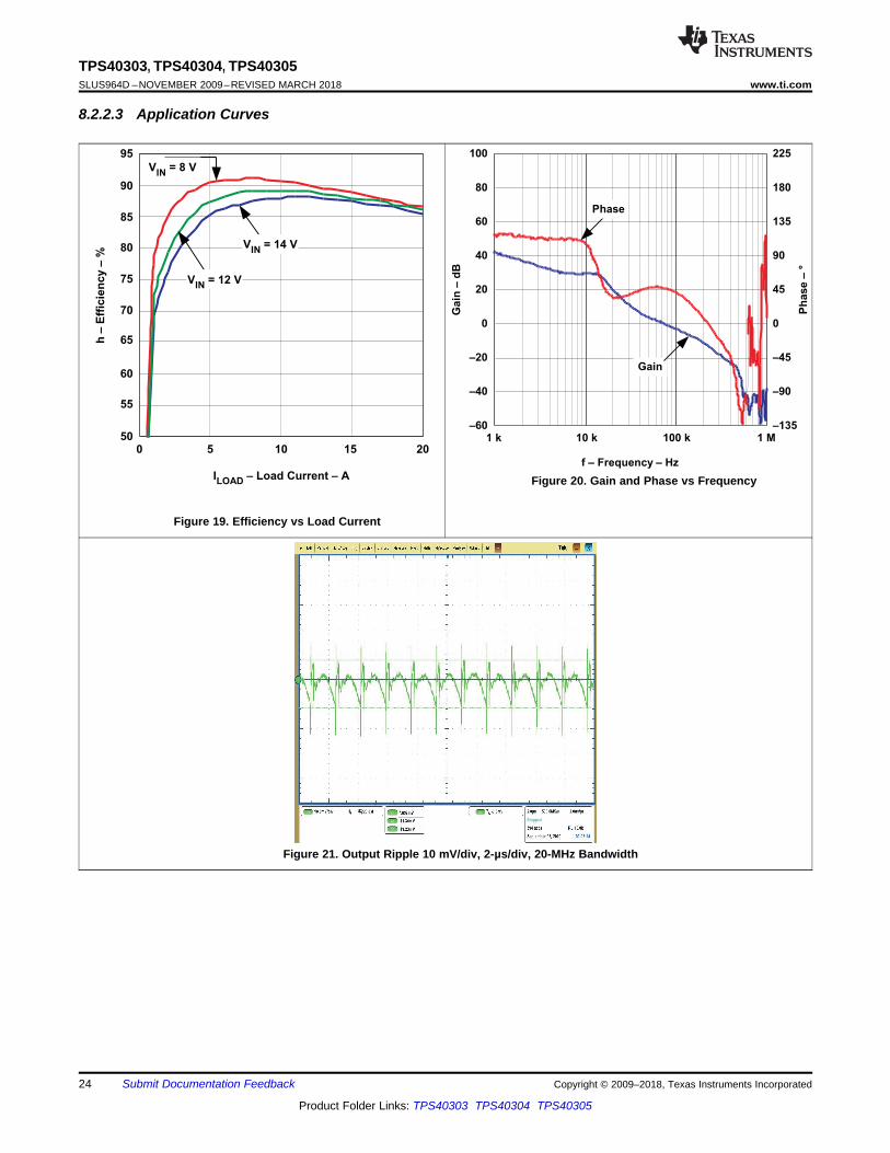
8.2.3.3 Application CurvesA typical efficiency graph for this design example using the TPS40303 is shown in Figure 23.The typical line andload regulation this design example using the TPS40303 is shown in Figure 24
Figure 23. Efficiency vs Load Current Figure 24. Line and Load Regulation
Figure 25. Total System Bode
9 Power Supply RecommendationsThese devices are designed to operate from an input voltage supply between 3 V and 20 V. This input supplyshould remain within the input voltage supply range. This supply must be well regulated.
10.1 Layout Guidelines• For MOSFET or Power Block Layout, follow the layout recommendations provided for the MOSFET or Power
Block selected.• Connect VDD to VIN as close as possible to the drain connection of the high-side FET to avoid introducing
additional drop which could trigger short-circuit protection.• Place VDD and BP to GND capacitors within 2 mm of the device and connected to the Thermal Pad (GND).• The FB to GND resistor should connect to the thermal tab (GND) with a minimum 10-mil wide trace.• Place VOUT to FB resistor within 2 mm of the FB pin.• The EN/SS-to-GND capacitor must connect to the thermal tab (GND) with a minimum 10-mil-wide trace. It
may share this trace with FB to GND.• If a BJT or MOSFET is used to disable EN/SS, place it within 5 mm of the device.• If a COMP to GND resistor is used, place it within 5 mm of the device.• All COMP and FB traces should be kept minimum line width and as short as possible to minimize noise
coupling.• Do not route EN/SS more than 20 mm from the device.• If multiple layers are used, extend GND under all components connected to FB, COMP and EN/SS to reduce
noise sensitivity.• HDRV and LDRV should provide short, low inductance paths of 5 mm or less to the gates of the MOSFETs or
Power Block.• No more than 1 Ω of resistance should be placed between HDRV or LDRV and their MOSFET or Power
Block gate pins.• LDRV / OC to GND Current Limit Programming resistor may be placed on the far side of the MOSFET if
necessary to ensure a short connection from LDRV to the gate of the low-side MOSFET.• The BOOT to SW resistor and capacitor should both be placed within 4 mm of the device using a minimum of
10-mil-wide trace. The full width of the component pads are preferred for trace widths if design rules allow.• If via must be used between the HDRV, SW and LDRV pins and their respective MOSFET or Power Block
connections, use a minimum of two vias to reduce parasitic inductance• Refer to the Land Pattern Data for the preferred layout of thermal vias within the thermal pad.• It is recommended to extend the top-layer copper area of the thermal pad (GND) beyond the package a
minimum 3 mm between pins 1 and 10 and 5 and 6 to improve thermal resistance to ambient of the device.
11.1.1 Third-Party Products DisclaimerTI'S PUBLICATION OF INFORMATION REGARDING THIRD-PARTY PRODUCTS OR SERVICES DOES NOTCONSTITUTE AN ENDORSEMENT REGARDING THE SUITABILITY OF SUCH PRODUCTS OR SERVICESOR A WARRANTY, REPRESENTATION OR ENDORSEMENT OF SUCH PRODUCTS OR SERVICES, EITHERALONE OR IN COMBINATION WITH ANY TI PRODUCT OR SERVICE.
11.2 Custom Design With WEBENCH® ToolsClick here to create a custom design using the TPS4030x devices with the WEBENCH® Power Designer.1. Start by entering the input voltage (VIN), output voltage (VOUT), and output current (IOUT) requirements.2. Optimize the design for key parameters such as efficiency, footprint, and cost using the optimizer dial.3. Compare the generated design with other possible solutions from Texas Instruments.
The WEBENCH Power Designer provides a customized schematic along with a list of materials with real-timepricing and component availability.
In most cases, these actions are available:• Run electrical simulations to see important waveforms and circuit performance• Run thermal simulations to understand board thermal performance• Export customized schematic and layout into popular CAD formats• Print PDF reports for the design, and share the design with colleagues
Get more information about WEBENCH tools at www.ti.com/WEBENCH.
11.3 Documentation Support
11.3.1 Related DocumentationThese references, design tools and links to additional references, including design software, may be found athttp://power.ti.com1. Additional PowerPAD™ information may be found in Applications Briefs (SLMA002) and (SLMA004).2. Under The Hood Of Low Voltage DC/DC Converters – SEM1500 Topic 5 – 2002 Seminar Series3. Understanding Buck Power Stages in Switchmode Power Supplies, (SLVA057), March 19994. Designing Stable Control Loops – SEM 1400 – 2001 Seminar Series
11.4 Related LinksThe table below lists quick access links. Categories include technical documents, support and communityresources, tools and software, and quick access to sample or buy.
Table 8. Related Links
PARTS PRODUCT FOLDER SAMPLE & BUY TECHNICALDOCUMENTS
TOOLS &SOFTWARE
SUPPORT &COMMUNITY
TPS40303 Click here Click here Click here Click here Click hereTPS40304 Click here Click here Click here Click here Click hereTPS40305 Click here Click here Click here Click here Click here
11.5 Receiving Notification of Documentation UpdatesTo receive notification of documentation updates, navigate to the device product folder on ti.com. In the upperright corner, click on Alert me to register and receive a weekly digest of any product information that haschanged. For change details, review the revision history included in any revised document.
11.6 Community ResourcesThe following links connect to TI community resources. Linked contents are provided "AS IS" by the respectivecontributors. They do not constitute TI specifications and do not necessarily reflect TI's views; see TI's Terms ofUse.
TI E2E™ Online Community TI's Engineer-to-Engineer (E2E) Community. Created to foster collaborationamong engineers. At e2e.ti.com, you can ask questions, share knowledge, explore ideas and helpsolve problems with fellow engineers.
Design Support TI's Design Support Quickly find helpful E2E forums along with design support tools andcontact information for technical support.
11.7 TrademarksE2E is a trademark of Texas Instruments.WEBENCH is a registered trademark of Texas Instruments.All other trademarks are the property of their respective owners.
11.8 Electrostatic Discharge CautionThese devices have limited built-in ESD protection. The leads should be shorted together or the device placed in conductive foamduring storage or handling to prevent electrostatic damage to the MOS gates.
11.9 GlossarySLYZ022 — TI Glossary.
This glossary lists and explains terms, acronyms, and definitions.
12 Mechanical, Packaging, and Orderable InformationThe following pages include mechanical, packaging, and orderable information. This information is the mostcurrent data available for the designated devices. This data is subject to change without notice and revision ofthis document. For browser-based versions of this data sheet, refer to the left-hand navigation.
TPS40303DRCR ACTIVE VSON DRC 10 3000 Green (RoHS& no Sb/Br)
CU NIPDAU |CU NIPDAUAG
Level-2-260C-1 YEAR -40 to 125 0303
TPS40303DRCT ACTIVE VSON DRC 10 250 Green (RoHS& no Sb/Br)
CU NIPDAU |CU NIPDAUAG
Level-2-260C-1 YEAR -40 to 125 0303
TPS40304DRCR ACTIVE VSON DRC 10 3000 Green (RoHS& no Sb/Br)
CU NIPDAUAG Level-2-260C-1 YEAR -40 to 125 0304
TPS40304DRCT ACTIVE VSON DRC 10 250 Green (RoHS& no Sb/Br)
CU NIPDAUAG Level-2-260C-1 YEAR -40 to 125 0304
TPS40305DRCR ACTIVE VSON DRC 10 3000 Green (RoHS& no Sb/Br)
CU NIPDAU |CU NIPDAUAG
Level-2-260C-1 YEAR -40 to 125 0305
TPS40305DRCT ACTIVE VSON DRC 10 250 Green (RoHS& no Sb/Br)
CU NIPDAU |CU NIPDAUAG
Level-2-260C-1 YEAR -40 to 125 0305
(1) The marketing status values are defined as follows:ACTIVE: Product device recommended for new designs.LIFEBUY: TI has announced that the device will be discontinued, and a lifetime-buy period is in effect.NRND: Not recommended for new designs. Device is in production to support existing customers, but TI does not recommend using this part in a new design.PREVIEW: Device has been announced but is not in production. Samples may or may not be available.OBSOLETE: TI has discontinued the production of the device.
(2) RoHS: TI defines "RoHS" to mean semiconductor products that are compliant with the current EU RoHS requirements for all 10 RoHS substances, including the requirement that RoHS substancedo not exceed 0.1% by weight in homogeneous materials. Where designed to be soldered at high temperatures, "RoHS" products are suitable for use in specified lead-free processes. TI mayreference these types of products as "Pb-Free".RoHS Exempt: TI defines "RoHS Exempt" to mean products that contain lead but are compliant with EU RoHS pursuant to a specific EU RoHS exemption.Green: TI defines "Green" to mean the content of Chlorine (Cl) and Bromine (Br) based flame retardants meet JS709B low halogen requirements of <=1000ppm threshold. Antimony trioxide basedflame retardants must also meet the <=1000ppm threshold requirement.
(3) MSL, Peak Temp. - The Moisture Sensitivity Level rating according to the JEDEC industry standard classifications, and peak solder temperature.
(4) There may be additional marking, which relates to the logo, the lot trace code information, or the environmental category on the device.
(5) Multiple Device Markings will be inside parentheses. Only one Device Marking contained in parentheses and separated by a "~" will appear on a device. If a line is indented then it is a continuationof the previous line and the two combined represent the entire Device Marking for that device.
(6) Lead/Ball Finish - Orderable Devices may have multiple material finish options. Finish options are separated by a vertical ruled line. Lead/Ball Finish values may wrap to two lines if the finishvalue exceeds the maximum column width.
Important Information and Disclaimer:The information provided on this page represents TI's knowledge and belief as of the date that it is provided. TI bases its knowledge and belief on informationprovided by third parties, and makes no representation or warranty as to the accuracy of such information. Efforts are underway to better integrate information from third parties. TI has taken andcontinues to take reasonable steps to provide representative and accurate information but may not have conducted destructive testing or chemical analysis on incoming materials and chemicals.TI and TI suppliers consider certain information to be proprietary, and thus CAS numbers and other limited information may not be available for release.
In no event shall TI's liability arising out of such information exceed the total purchase price of the TI part(s) at issue in this document sold by TI to Customer on an annual basis.
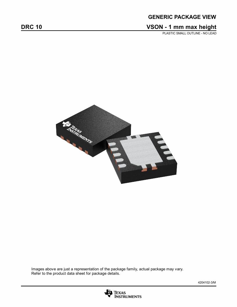
Images above are just a representation of the package family, actual package may vary.Refer to the product data sheet for package details.
DRC 10 VSON - 1 mm max heightPLASTIC SMALL OUTLINE - NO LEAD
4204102-3/M
www.ti.com
PACKAGE OUTLINE
C
10X 0.300.18
2.4 0.1
2X2
1.65 0.1
8X 0.5
1.00.8
10X 0.50.3
0.050.00
A 3.12.9
B
3.12.9
(0.2) TYP4X (0.25)
2X (0.5)
VSON - 1 mm max heightDRC0010JPLASTIC SMALL OUTLINE - NO LEAD
4218878/B 07/2018
PIN 1 INDEX AREA
SEATING PLANE
0.08 C
1
5 6
10
(OPTIONAL)PIN 1 ID 0.1 C A B
0.05 C
THERMAL PADEXPOSED
SYMM
SYMM11
NOTES: 1. All linear dimensions are in millimeters. Any dimensions in parenthesis are for reference only. Dimensioning and tolerancing per ASME Y14.5M. 2. This drawing is subject to change without notice. 3. The package thermal pad must be soldered to the printed circuit board for optimal thermal and mechanical performance.
SCALE 4.000
www.ti.com
EXAMPLE BOARD LAYOUT
0.07 MINALL AROUND0.07 MAX
ALL AROUND
10X (0.24)
(2.4)
(2.8)
8X (0.5)
(1.65)
( 0.2) VIATYP
(0.575)
(0.95)
10X (0.6)
(R0.05) TYP
(3.4)
(0.25)
(0.5)
VSON - 1 mm max heightDRC0010JPLASTIC SMALL OUTLINE - NO LEAD
4218878/B 07/2018
SYMM
1
5 6
10
LAND PATTERN EXAMPLEEXPOSED METAL SHOWN
SCALE:20X
11SYMM
NOTES: (continued) 4. This package is designed to be soldered to a thermal pad on the board. For more information, see Texas Instruments literature number SLUA271 (www.ti.com/lit/slua271).5. Vias are optional depending on application, refer to device data sheet. If any vias are implemented, refer to their locations shown on this view. It is recommended that vias under paste be filled, plugged or tented.
SOLDER MASKOPENINGSOLDER MASK
METAL UNDER
SOLDER MASKDEFINED
EXPOSED METAL
METALSOLDER MASKOPENING
SOLDER MASK DETAILS
NON SOLDER MASKDEFINED
(PREFERRED)
EXPOSED METAL
www.ti.com
EXAMPLE STENCIL DESIGN
(R0.05) TYP
10X (0.24)
10X (0.6)
2X (1.5)
2X(1.06)
(2.8)
(0.63)
8X (0.5)
(0.5)
4X (0.34)
4X (0.25)
(1.53)
VSON - 1 mm max heightDRC0010JPLASTIC SMALL OUTLINE - NO LEAD
4218878/B 07/2018
NOTES: (continued) 6. Laser cutting apertures with trapezoidal walls and rounded corners may offer better paste release. IPC-7525 may have alternate design recommendations.
SOLDER PASTE EXAMPLEBASED ON 0.125 mm THICK STENCIL
EXPOSED PAD 11:
80% PRINTED SOLDER COVERAGE BY AREASCALE:25X
SYMM
1
56
10
EXPOSED METALTYP11
SYMM
IMPORTANT NOTICE
Texas Instruments Incorporated (TI) reserves the right to make corrections, enhancements, improvements and other changes to itssemiconductor products and services per JESD46, latest issue, and to discontinue any product or service per JESD48, latest issue. Buyersshould obtain the latest relevant information before placing orders and should verify that such information is current and complete.TI’s published terms of sale for semiconductor products (http://www.ti.com/sc/docs/stdterms.htm) apply to the sale of packaged integratedcircuit products that TI has qualified and released to market. Additional terms may apply to the use or sale of other types of TI products andservices.Reproduction of significant portions of TI information in TI data sheets is permissible only if reproduction is without alteration and isaccompanied by all associated warranties, conditions, limitations, and notices. TI is not responsible or liable for such reproduceddocumentation. Information of third parties may be subject to additional restrictions. Resale of TI products or services with statementsdifferent from or beyond the parameters stated by TI for that product or service voids all express and any implied warranties for theassociated TI product or service and is an unfair and deceptive business practice. TI is not responsible or liable for any such statements.Buyers and others who are developing systems that incorporate TI products (collectively, “Designers”) understand and agree that Designersremain responsible for using their independent analysis, evaluation and judgment in designing their applications and that Designers havefull and exclusive responsibility to assure the safety of Designers' applications and compliance of their applications (and of all TI productsused in or for Designers’ applications) with all applicable regulations, laws and other applicable requirements. Designer represents that, withrespect to their applications, Designer has all the necessary expertise to create and implement safeguards that (1) anticipate dangerousconsequences of failures, (2) monitor failures and their consequences, and (3) lessen the likelihood of failures that might cause harm andtake appropriate actions. Designer agrees that prior to using or distributing any applications that include TI products, Designer willthoroughly test such applications and the functionality of such TI products as used in such applications.TI’s provision of technical, application or other design advice, quality characterization, reliability data or other services or information,including, but not limited to, reference designs and materials relating to evaluation modules, (collectively, “TI Resources”) are intended toassist designers who are developing applications that incorporate TI products; by downloading, accessing or using TI Resources in anyway, Designer (individually or, if Designer is acting on behalf of a company, Designer’s company) agrees to use any particular TI Resourcesolely for this purpose and subject to the terms of this Notice.TI’s provision of TI Resources does not expand or otherwise alter TI’s applicable published warranties or warranty disclaimers for TIproducts, and no additional obligations or liabilities arise from TI providing such TI Resources. TI reserves the right to make corrections,enhancements, improvements and other changes to its TI Resources. TI has not conducted any testing other than that specificallydescribed in the published documentation for a particular TI Resource.Designer is authorized to use, copy and modify any individual TI Resource only in connection with the development of applications thatinclude the TI product(s) identified in such TI Resource. NO OTHER LICENSE, EXPRESS OR IMPLIED, BY ESTOPPEL OR OTHERWISETO ANY OTHER TI INTELLECTUAL PROPERTY RIGHT, AND NO LICENSE TO ANY TECHNOLOGY OR INTELLECTUAL PROPERTYRIGHT OF TI OR ANY THIRD PARTY IS GRANTED HEREIN, including but not limited to any patent right, copyright, mask work right, orother intellectual property right relating to any combination, machine, or process in which TI products or services are used. Informationregarding or referencing third-party products or services does not constitute a license to use such products or services, or a warranty orendorsement thereof. Use of TI Resources may require a license from a third party under the patents or other intellectual property of thethird party, or a license from TI under the patents or other intellectual property of TI.TI RESOURCES ARE PROVIDED “AS IS” AND WITH ALL FAULTS. TI DISCLAIMS ALL OTHER WARRANTIES ORREPRESENTATIONS, EXPRESS OR IMPLIED, REGARDING RESOURCES OR USE THEREOF, INCLUDING BUT NOT LIMITED TOACCURACY OR COMPLETENESS, TITLE, ANY EPIDEMIC FAILURE WARRANTY AND ANY IMPLIED WARRANTIES OFMERCHANTABILITY, FITNESS FOR A PARTICULAR PURPOSE, AND NON-INFRINGEMENT OF ANY THIRD PARTY INTELLECTUALPROPERTY RIGHTS. TI SHALL NOT BE LIABLE FOR AND SHALL NOT DEFEND OR INDEMNIFY DESIGNER AGAINST ANY CLAIM,INCLUDING BUT NOT LIMITED TO ANY INFRINGEMENT CLAIM THAT RELATES TO OR IS BASED ON ANY COMBINATION OFPRODUCTS EVEN IF DESCRIBED IN TI RESOURCES OR OTHERWISE. IN NO EVENT SHALL TI BE LIABLE FOR ANY ACTUAL,DIRECT, SPECIAL, COLLATERAL, INDIRECT, PUNITIVE, INCIDENTAL, CONSEQUENTIAL OR EXEMPLARY DAMAGES INCONNECTION WITH OR ARISING OUT OF TI RESOURCES OR USE THEREOF, AND REGARDLESS OF WHETHER TI HAS BEENADVISED OF THE POSSIBILITY OF SUCH DAMAGES.Unless TI has explicitly designated an individual product as meeting the requirements of a particular industry standard (e.g., ISO/TS 16949and ISO 26262), TI is not responsible for any failure to meet such industry standard requirements.Where TI specifically promotes products as facilitating functional safety or as compliant with industry functional safety standards, suchproducts are intended to help enable customers to design and create their own applications that meet applicable functional safety standardsand requirements. Using products in an application does not by itself establish any safety features in the application. Designers mustensure compliance with safety-related requirements and standards applicable to their applications. Designer may not use any TI products inlife-critical medical equipment unless authorized officers of the parties have executed a special contract specifically governing such use.Life-critical medical equipment is medical equipment where failure of such equipment would cause serious bodily injury or death (e.g., lifesupport, pacemakers, defibrillators, heart pumps, neurostimulators, and implantables). Such equipment includes, without limitation, allmedical devices identified by the U.S. Food and Drug Administration as Class III devices and equivalent classifications outside the U.S.TI may expressly designate certain products as completing a particular qualification (e.g., Q100, Military Grade, or Enhanced Product).Designers agree that it has the necessary expertise to select the product with the appropriate qualification designation for their applicationsand that proper product selection is at Designers’ own risk. Designers are solely responsible for compliance with all legal and regulatoryrequirements in connection with such selection.Designer will fully indemnify TI and its representatives against any damages, costs, losses, and/or liabilities arising out of Designer’s non-compliance with the terms and provisions of this Notice.