An IMPORTANT NOTICE at the end of this data sheet addresses availability, warranty, changes, use in safety-critical applications,intellectual property matters and other important disclaimers. PRODUCTION DATA.
TPS54A20SLVSCQ8A –DECEMBER 2015–REVISED APRIL 2016
TPS54A20 8-V to 14-V Input, 10-A, up to 10-MHz SWIFT™ Step Down Converter
1
1 Features1• Two-phase, Synchronous Series Capacitor Buck
Converter• Automatic Current Balancing Between Phases• 2-MHz to 5-MHz Per Phase Switching Frequency• 14-ns Minimum On-Time• 0.51-V to 2-V Output Voltage Range with ±0.5%
Feedback Reference Voltage• Input Overvoltage Lockout for 17-V Surge
Protection• Adjustable Current Limit with Auto Restart
(Hiccup)• Synchronizes to an External Clock• Fixed Frequency in Steady State• Adaptive On-Time Control• Internal Feedback Loop Compensation• Internal Gate Drive LDO with External Supply
Option• EN Pin Allowing for Adjustable Input UVLO• Selectable Soft-Start Time• Monotonic Startup with Pre-biased Output• Output Power Good Indicator (Open Drain)• Output Overvoltage/Undervoltage Protection
2 Applications• Telecom, base station, and communications
routers, and other networking equipment• Low profile/Backside board mounting (< 2 mm
height)
3 DescriptionThe TPS54A20 is a two-phase, synchronous seriescapacitor buck converter designed for small size, lowvoltage applications from a 12-V input rail. Thistopology uniquely merges a switched capacitor circuitwith a two phase buck converter. Advantages includeautomatic current balancing between the inductors,lower switching losses which enable high frequency(HF) operation, and voltage step-down through theseries capacitor. Small, low profile inductors usedwith the TPS54A20 significantly reduce total solutionarea and height. An adaptive on-time controlarchitecture provides fast transient response andaccurate voltage regulation at up to 10-MHz operatingfrequency. Fixed frequency operation during steadystate is maintained through the use of a phase lockloop (PLL) to lock switching signals to a referenceoscillator.
Device Information(1)
PART NUMBER PACKAGE BODY SIZE (NOM)TPS54A20 VQFN (20 pins) 3.5 mm x 4 mm
(1) For all available packages, see the orderable addendum atthe end of the datasheet.
Simplified SchematicEfficiency vs Load Current
1.8 VOUT, 2 MHz per phase, External VG+,3.2 x 2.5 x 1.2 mm inductors
9 Power Supply Recommendations ...................... 3110 Layout................................................................... 32
10.1 Layout Guidelines ................................................. 3210.2 Layout Example .................................................... 33
11 Device and Documentation Support ................. 3511.1 Documentation Support ........................................ 3511.2 Community Resources.......................................... 3511.3 Trademarks ........................................................... 3511.4 Electrostatic Discharge Caution............................ 3511.5 Glossary ................................................................ 35
12 Mechanical, Packaging, and OrderableInformation ........................................................... 35
4 Revision History
Changes from Original (December 2015) to Revision A Page
• Changed the device status to Production data. .................................................................................................................... 1
(1) I = Input, O = Output, S = Supply, G = Ground Return
5 Pin Configuration and Functions
RNJ PackageVQFN (20 Pin)
Top View
Pin FunctionsPIN
I/O (1) DESCRIPTIONNAME NO.
AGND 1 G Analog signal ground of the IC. AGND should be connected to PGND and VG- at a single point on PCB(e.g. underneath the IC).
BOOTA 8 S Bootstrap capacitor node for phase A high-side MOSFET gate driver. Connect the bootstrap capacitorfrom this pin to the SCAP pin (pin 9).
BOOTB 10 S Bootstrap capacitor node for phase B high-side MOSFET gate driver. Connect the bootstrap capacitorfrom this pin to the SWB pin.
EN 4 I Enable pin. Floating this pin will enable the IC. Pull below 1.23V to enter shutdown mode. Can also beused to adjust the input undervoltage lockout above 8 V with two resistors.
FB 18 I Feedback pin for voltage regulation. Connect this pin to the center tap of a resistor divider to set theoutput voltage.
ILIM 5 I Current limit programming pin. A resistor between this pin and ground sets the current limit. If no resistoris included, the default load current limit is 15 A.
NC 11 No connect. This pin is not electrically connected to the IC and is included for board level reliability (BLR)purposes. Connect this pin to the SCAP trace.
PGND 2 G Power ground of the IC. PGND should be connected to AGND and VG- at a single point on PCB (e.g.underneath the IC). Thermal vias to internal ground planes should be added beneath this pin.
PGOOD 15 O
Power good indicator. This pin is an open-drain output and will assert low if the output voltage is greaterthan ±5% away from the desired value or due to thermal shutdown, over-voltage/under-voltage, ENshutdown, or during soft start. A pull-up resistor can be connected between PGOOD and VG+ or anexternal logic supply pin.
SCAP 9,20 O Series capacitor pin. Connect a ceramic capacitor from pin 20 to the SWA pin.
SS/FSEL 6 ISoft start/frequency select pin. Connect a resistor from this pin to ground to set the soft-start time and theswitching frequency. If no resistor is provided, the default setting of 4MHz oscillator frequency and 512µssoft start time is used.
SWA 13 O Switching node for phase A. Connect an inductor from this pin to the output capacitors.
SWB 12 O Switching node for phase B. Connect an inductor from this pin to the output capacitors.
SYNC 14 I External clock synchronization pin. An external clock signal can be connected to this pin to synchronizethe oscillator frequency (within ±10% of the nominal frequency set via SS/FSEL).
TON 19 I On-time selection. An external resistor from this pin to the AGND pin programs the nominal on-time of thehigh side switches.
VG+ 16 SGate driver positive supply pin. Connect a bypass capacitor from this pin to VG-. To improve converterefficiency, the internal regulator can be overridden by connecting an external 5V supply to this pin. Thissupply rail also provides power to the control circuitry.
VG- 17 G Gate driver supply return pin. VG- should be connected to PGND and AGND at a single point on PCB(e.g. underneath the IC).
VGA 7 S High side phase A gate driver supply pin. Connect a bypass capacitor from this pin to ground.
VIN 3 I The power input pin to the IC. Connect VIN to a supply voltage between 8 V and 14 V.
(1) Stresses beyond those listed under Absolute Maximum Ratings may cause permanent damage to the device. These are stress ratingsonly, which do not imply functional operation of the device at these or any other conditions beyond those indicated under RecommendedOperating Conditions. Exposure to absolute-maximum-rated conditions for extended periods may affect device reliability.
6 Specifications
6.1 Absolute Maximum Ratingsover operating free-air temperature range (unless otherwise noted) (1)
MIN MAX UNIT
Input Voltage
Power Conversion, VINDC w.r.t. PGND, switching –0.3 15
VDC w.r.t. PGND, non-switching –0.3 17
Bootstrap, V(BOOTA)DC with respect to PGND –0.3 22 VDC with respect to SCAP 6 V
Bootstrap, V(BOOTB)DC with respect to PGND –0.3 14 VDC with respect to SWB 6 V
Bias Supply, VG DC with respect to PGND –0.3 6 VSeries Capacitor Node Voltage,V(SCAP)
DC with respect to PGND –0.3 16
VSwitch Node Voltage, V(SWA,SWB)
DC with respect to PGND –1 9Pulse < 10 ns –4 14
Feedback, V(FB) –0.3 3 VOutput Voltage Bias Supply, V(VGA) DC with respect to PGND –0.3 15 V
(1) JEDEC document JEP155 states that 500-V HBM allows safe manufacturing with a standard ESD control process.(2) JEDEC document JEP157 states that 250-V CDM allows safe manufacturing with a standard ESD control process.
6.2 ESD RatingsVALUE UNIT
V(ESD) Electrostatic dischargeHuman body model (HBM), per ANSI/ESDA/JEDEC JS-001, all pins (1) ±2000
VCharged device model (CDM), per JEDEC specification JESD22-C101,all pins (2) ±500
6.3 Recommended Operating Conditionsover operating free-air temperature range (unless otherwise noted)
MIN NOM MAX UNITVIN Input Voltage 8 14 VVOUT Output Voltage 0.5 VIN/5 VIOUT Output Current 0 10 ATJ Junction Temperature -40 125 °C
(1) For more information about traditional and new thermal metrics, see the IC Package Thermal Metrics application report, SPRA953.(2) Tested on four layer evaluation board.
PGOOD sink current V(PGOOD) = 0.4 V 2.7 mAPGOOD pin leakage current VFB = VREF, V(PGOOD)= 5 V 1 μAMinimum VIN for valid PGOOD V(PGOOD) ≤ 0.5 V at 100 µA 1.2 2.75 V
THERMAL SHUTDOWNThermal shutdown set threshold 135 °CThermal shutdown hysteresis 20 °C
ENABLE (EN PIN)Enable to Start Switching time 1 µF series cap, VIN = 12V 625 µsSYNCLock in time 30 µsHIGH-SIDE MOSFETSSW minimum ON pulse width 14 nsSW minimum OFF pulse width 10 nsNon-Overlap Time between HS FETOff and LS FET On (deadtime)
Fsw = 5 MHz, VIN = 12 V
3 ns
Non-Overlap Time between LS FETOff and HS FET On (deadtime)
7.1 OverviewThe TPS54A20 is a 14-V, 10-A, synchronous series capacitor step-down (buck) converter with four integrated N-channel MOSFETs. To improve performance during line and load transients the TPS54A20 implements anadaptive on-time control scheme which does not require external compensation components. The selectableswitching frequencies are 2 MHz, 3.5 MHz, or 5 MHz per phase which allows for efficiency and size optimizationwhen selecting the output filter components. A resistor to ground on the TON pin sets the nominal high sideswitch on-time based on the desired output voltage.
The TPS54A20 contains an internal oscillator for steady-state, fixed frequency operation that is set through theSS/FSEL pin. The controller operates at twice the per phase switching frequency (that is, 4 MHz, 7 MHz, or 10MHz) and the oscillator is set accordingly. An external synchronization clock can also be provided via the SYNCpin.
The TPS54A20 starts up safely into loads with pre-biased outputs (non-zero volts at startup). The deviceimplements an internal under voltage lockout (UVLO) feature on the VIN pin with a nominal starting voltage of7.65 V. The total operating current for the TPS54A20 is approximately 6 mA when not switching and under noload. When the TPS54A20 is disabled by pulling the EN pin low, the supply current is typically less than 50 µA.
The integrated MOSFETs allow for high-efficiency, high-density power supply designs with continuous outputcurrents up to 10 A. The MOSFETs are sized to optimize efficiency for low duty cycle applications operatingaround 2 MHz per phase switching frequency.
The TPS54A20 reduces the external component count by integrating the bootstrap recharge circuit. Capacitorsconnected between the BOOTA/BOOTB and SCAP/SWB pins (respectively) supply the gate drive voltage for theintegrated high-side MOSFETs. The output voltage can be stepped down to as low as the 0.5-V voltagereference (VREF).
The TPS54A20 has a power good comparator (PGOOD) which monitors the output voltage through the FB pin.The PGOOD pin is an open-drain MOSFET which is pulled low when the FB pin voltage is less than 95% orgreater than 105% of the reference voltage (VREF). The PGOOD pin floats (de-asserted) when the FB pin voltageis between 95% to 105% of VREF. The PGOOD pin is held low during startup or when a fault occurs.
The EN pin is used to provide power supply sequencing during power up. Soft start times for each frequency canbe selected through the SS/FSEL pin. Soft start helps to minimize inrush currents.
The device current limit can be set via the ILIM pin. Two selectable current limits are provided.
The control scheme implemented is an adaptive on-time control. The on-time is adjusted based on input voltageand oscillator frequency. An internal phase lock loop (PLL) ensures fixed-frequency operation of the converterover the entire load range and adapts the on-time accordingly.
7.3.1 Frequency SelectionThe oscillator frequency of this converter can be selected to be one of three options: 4, 7, or 10 MHz. The perphase switching frequency of the converter is half the oscillator frequency (that is, 2, 3.5, or 5 MHz per phase).The internal oscillator frequency is selected by programming the SS/FSEL pin. The resistor programminginformation is shown in Table 1. The frequency setting is latched in at power up and cannot be changed duringoperation. Cycling the input power or the EN pin will reset the frequency setting.
7.3.2 External Clock SyncronizationAn external clock can be connected to the SYNC pin. The external clock signal overrides the internal oscillatorand is used as the system clock. This feature enables the user to synchronize the switching events to a masterclock on their board and reduce/manage the ripple on the input capacitors. The internal phase locked loop (PLL)has been implemented to allow synchronization at frequencies between ±10% of the nominal oscillator frequencyprogrammed on the SS/FSEL pin. This allows the user to easily switch from the internal oscillator mode to theexternal clock mode. Before the external clock is present or after it is removed, the device with default to theinternal oscillator setting as programmed on the SS/FSEL pin.
To implement the synchronization feature, connect a square wave clock signal to the SYNC pin with a duty cyclebetween 20% and 80%. The clock signal amplitude must transition lower than 0.8 V and higher than 2 V. Thestart of the switching cycle is synchronized to the rising edge of the SYNC pin. The device can be configured foroperation in applications where both an internal oscillator mode and an external synchronization clock mode areneeded. Before the external clock is present, the device functions with the internal oscillator and the switching
Feature Description (continued)frequency is set by the RSS/FSEL resistor. When the external clock is present, the SYNC mode overrides theinternal oscillator. The first time the SYNC pin is pulled above the SYNC high threshold (2 V), the deviceswitches from the internal oscillator mode to the SYNC mode and the PLL starts to lock onto the frequency of theexternal clock. When the external SYNC clock is removed, the converter will transition back to the internaloscillator after 4 internal clock cycles.
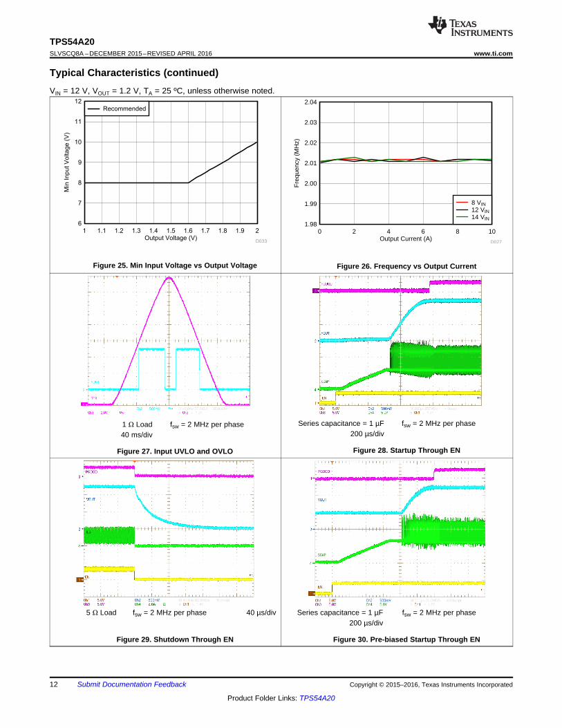
7.3.3 Adjusting the Output VoltageThe output voltage is set by connecting a resistor divider network from the output voltage to the FB pin of thedevice and to AGND. It is recommended that the lower divider resistor maintain a range between 1 kΩ and 10kΩ. To change the output voltage of a design, it is necessary to select the value of the upper resistor. Equation 2can be used to select the upper resistor. Selecting the value of the upper resistor can change the output voltagebetween 0.508 V and 2 V. The minimum output setpoint voltage cannot be less than the reference voltage of0.508 V. The maximum output voltage can be limited by minimum input voltage as shown in Figure 24. Therecommended minimum input voltage should be at least five times the output voltage as shown in Figure 25.This is due to the nature of the series capacitor buck converter.
7.3.4 Soft StartSoft start is an important feature that limits current inrush into the converter and reduces the load on the busconverter that supplies this device. During soft start, the internal reference voltage is slowly ramped up to thenominal internal reference voltage (~0.5 V). This slowly increases the commanded output voltage of theconverter and reduces the initial surge in current. PGOOD remains low during soft start, the PLL is not active,and output UVP/OVP faults are disabled. After the soft start interval is complete, the converter operates withnormal operating conditions and PGOOD will no longer be held low when the output is within bounds.
Soft-start time is programmed with an external resistor on SS/FSEL pin (or by shorting to ground or by leavingthe pin open). There are multiple soft-start time options per operating frequency available to the user through theSS/FSEL pin. The soft-start setting is latched in at power up or when the EN pin voltage is set high. Resistorsused for programing the SS/FSEL pin must have ±1% or lower tolerance. The following frequencies and soft starttimes can be programmed on the SS/FSEL pin.
Table 1. Frequency and Soft Start Resistor Selection
7.3.5 Startup into Pre-biased OutputsThe device prevents the low-side MOSFETs from discharging a pre-biased output. During pre-biased startup, thelow-side MOSFETs do not turn on until after the phase A high-side MOSFET has started switching. The high-side MOSFETs do not start switching until the internal soft-start reference voltage exceeds the voltage at the FBpin. It is required to first apply the gate driver supply voltage (VG+) before starting up into pre-biased loads.Alternatively, 6.8 µF bypass capacitance or more can be used.
7.3.6 Power Good (PGOOD)The Power Good (PGOOD) pin is an open drain output. After startup when the FB pin is typically between 95%and 105% of the internal voltage reference, the PGOOD pin pull-down is de-asserted and the pin floats. It isrecommended to use a pullup resistor between the values of 10 kΩ and 100 kΩ to a voltage source that is 5.5 Vor less. The PGOOD is in a defined state once the VIN input voltage is greater than approximately 1.2 V but withreduced current sinking capability. The PGOOD achieves full current sinking capability once the VIN inputvoltage is above the input UVLO. The PGOOD pin is pulled low when the FB pin voltage is typically lower than95% or greater than 105% of the nominal internal reference voltage. A resistor-capacitor (RC) filter can beconnected to the PGOOD pin to filter out PGOOD being pulled low during large load transients if low outputcapacitance is used. The PGOOD pin is also pulled low if a fault is detected, the EN pin is pulled low, or theconverter is performing its soft-start power up sequence.
7.3.7 Overcurrent ProtectionThe device protects itself from an overcurrent condition by a current limit detector. The device senses inductorcurrents using the low side MOSFETs. After three sequential overcurrent measurements are made (in phase Aor B), the over current flag is triggered, the converter switches are turned off, and PGOOD is pulled low. Theconverter attempts to restart after a hiccup interval counter has expired (that is, 32.8 ms, 18.7 ms, or 13.1 mswhen in 4 MHz, 7 MHz, or 10 MHz mode, respectively). This provides a hiccup response to an overcurrentcondition.
The two overcurrent trip points are based on two full load applications of 7.5 A or 10 A. The overcurrent trippoints correspond to the load demanding 1.5 times the full load current (11.25 A and 15 A, respectively). Thisprovides enough margin for brief overshoots in inductor currents during a load transient while at the same timeprotecting against short circuits or other potentially catastrophic faults on the output. The table below lists theresistor values for programming the ILIM pin to select the desired overcurrent limit. Programming resistors withup to ±5% variation can be used. The current limit selection is latched in at power up and cannot be changedwithout cycling power input or the EN pin voltage.
Table 2. Current Limit SelectionRILIM (kΩ) Load Current Limit (A)
Open 1547 11.25
7.3.8 Light Load OperationThe converter operates in forced continuous conduction mode (FCCM) under light load conditions. Whenoperating in FCCM, the high side and low side MOSFETs are turned on and off in a complementary fashion andnegative inductor current is allowed for part of the switching cycle. The switching frequency remains constant inFCCM.
7.3.9 Output Undervoltage/Overvoltage ProtectionThe device incorporates an output undervoltage/overvoltage protection (UVP/OVP) circuit to prevent damage tothe load. This fault can be triggered during large, fast load transients if insufficient output capacitance is used.The UVP/OVP feature compares the FB pin voltage to internal thresholds. If the FB pin voltage is lower than90% or greater than 110% of the nominal internal reference voltage, the converter is turned off (i.e. powerMOSFETs are turned OFF), a fault is triggered, and the PGOOD pin is pulled low. When the fault hiccup intervalis complete, the converter will attempt to restart.
7.3.10 Input Undervoltage/Overvoltage LockoutThe device incorporates an input undervoltage/overvoltage lockout (UVLO/OVLO) circuit. The converter will notoperate if the input voltage is below the UVLO threshold. The OVLO circuit protects the converter if the input busvoltage flies higher than the input voltage rating of the device while it is switching. When the input voltagecrosses the input rising OVLO trip threshold, the converter turns off all the switches (makes them highimpedance) and PGOOD is pulled low. When the input voltage drops lower than the falling OVLO threshold, theconverter restarts using the normal soft-start sequence. This feature increases the maximum input voltage thedevice can sustain without being damaged due to a fault in the system.
7.3.11 Enable and Adjusting Undervoltage LockoutThe EN pin provides electrical on and off control of the device. Once the EN pin voltage exceeds the thresholdvoltage, the device starts operation. If the EN pin voltage is pulled below the threshold voltage, the regulatorstops switching and enters a low power state. There is no voltage hysteresis in the EN threshold. The rising andfalling voltage thresholds occur at the same level.
The EN pin has an internal hysteretic current source. This allows the user to float the EN pin for self-enabling thedevice or to design the ON and OFF threshold input voltages with a resistor divider at the EN pin. If anapplication requires controlling the EN pin, use open drain or open collector output logic to interface with the pin.
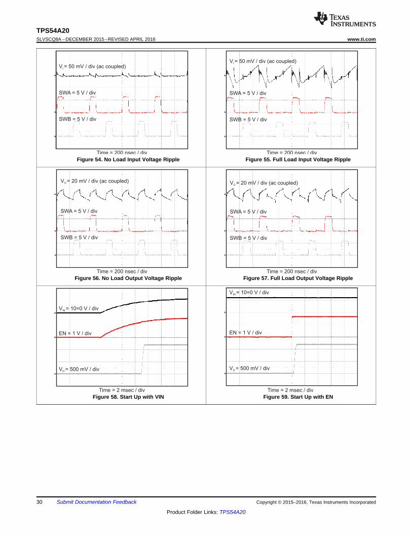
The EN pin can be configured as shown in Figure 42. The EN pin has a 1 µA pull-up current iP which sets thecurrent source value before the start-up sequence. The device includes the second 3 µA current source iH whichis activated when the EN threshold voltage has been exceeded. To achieve clean transitions between the OFFand ON states, it is recommended that the turn OFF threshold is no less than 7.75 V, and the turn ON thresholdis no less than 8 V on the VIN pin. It is also recommended to set the UVLO hysteresis to be greater than 500mVin order to avoid repeated chatter during start up or shut down. The value of REN(TOP) and REN(BOT) can becalculated using Equation 18 and Equation 19 as described in the applications section.
Figure 42. Adjustable VIN Undervoltage Lockout
7.3.12 Series Capacitor MonitoringThe series capacitor voltage is preconditioned and monitored during operation. The series capacitor is locatedbetween the source of the high-side MOSFET and the drain of the low-side MOSFET in Phase A . After the inputvoltage is above UVLO and the EN pin is high, the series capacitor is precharged. A 10 mA current sourcecharges the series capacitor up to half the input voltage. When the series capacitor precharge is complete, thesoft start sequence begins. The delay due series capacitor precharge can be calculated using Equation 1.
(1)
Here Ct is the series capacitance, Ipc is the precharge current, and VIN is the input voltage.
The voltage monitor is continuously tracking the status of the series capacitor. Its function is to ensure the seriescapacitor voltage, measured differentially between the SCAP pin and the SWA pin, stays within predefinedthresholds. These thresholds are relative to the VIN voltage with respect to PGND and set at 35% and 65% ofVIN. If the voltage monitor indicates a voltage outside of these thresholds has occurred, a fault is triggered andfollowing actions are taken based on which threshold has been crossed.
7.3.12.1 Dropping Below 35% ThresholdThe 35% of VIN threshold detects a series capacitor undervoltage fault. Once the 35% threshold is breached, afault is triggered, the converter shuts down, and PGOOD is pulled low. After the fault hiccup time is complete, theconverter will start up in the normal manner. The start up sequence begins with pre-charging the series capacitorto half the input voltage and is followed by the soft start.
7.3.12.2 Rising Above 65% ThresholdThe 65% of VIN threshold indicates a series capacitor overvoltage fault has occurred. Once the 65% threshold isbreached, a fault is triggered, the converter shuts down, PGOOD is pulled low, and an internal bleed resistor isconnected to the SCAP to reduce the series capacitor voltage. After the fault hiccup time is complete, theconverter will start up in the normal manner.
7.3.13 Thermal ShutdownThe die temperature is continuously monitored to ensure it is within limits. The thermal shutdown (TSD) fault istriggered when the die temperature exceeds the rising temperature threshold. This interrupts switching by makingthe switches high impedance. The fault state persists until the die temperature cools down to below the fallingtemperature threshold. The converter then automatically goes through the normal soft start sequence.
7.3.14 Phase A Power StagePhase A implements a bootstrap driver for the high-side MOSFET, an LDO, a low-side driver and a low-sidecurrent monitor. Additional logic is included to implement deadtime control and overcurrent protection.
An LDO is implemented to manage the high-side bootstrap driver. This LDO is unique to this topology given thehigh-side driver is referenced to the SCAP pin and not to the conventional switch node of a buck converter. Aconventional bootstrap circuit will not work because the SCAP pin is never connected to PGND during operation.The LDO is designed to produce an output voltage at the VGA pin. This allows a nominal enhancement ofaround 5V about the VIN rail. The bootstrap capacitor charges when the phase A low side switch is on. Anexternal decoupling capacitor is required on the VGA pin.
The low-side MOSFET current is monitored using a sense FET configuration. This circuit enables the driver tomonitor the current delivered in Phase A for overcurrent protection. In the case of overcurrent, a fault flag is set ifthe current detected exceeds the current limit threshold. Adjustment of this threshold is accomplished viaprogramming the ILIM pin.
7.3.15 Phase B Power StagePhase B implements a bootstrap driver for the high-side MOSFET, a low-side driver and a low-side currentmonitor. Additional logic is included to implement deadtime control and overcurrent protection.
No additional LDO function is required for Phase B as the bootstrap capacitor is charged directly from the VGinput rail. A conventional bootstrap circuit is used in phase B.
The overcurrent protection operates in the same manner as Phase A.
7.3.16 Internal Gate Drive RegulatorThere is an internal linear regulator that generates a 4.8 V supply rail on the VG+ pin. The input comes from theVIN pin. The VG+ supply rail is used to power the gate drivers of phase A low side switch and phase B switches.It also is the input to another regulator that generates the internal supply rails used by the controller. To improveconverter efficiency, an external 5V supply is recommended to be connected to the VG+ pin, thereby overridingthe internal 4.8 V regulator. The VG+ supply requires external decoupling capacitance connected between theVG+ and VG- pins. The VG- pin must be connected to AGND and PGND. It is recommended to make thisconnection directly beneath the device.
7.3.17 Voltage Feed ForwardThe input voltage feed forward (VFF) circuit adapts the nominal on-time of the converter in response to changesin the input voltage. The VFF provides a control signal to the on-time generator based on the value of the resistorplaced on the TON pin and the input voltage.
7.3.18 Internal OscillatorThe internal oscillator provides a default system clock for the converter. The oscillator can be programmed to runat 4 MHz, 7 MHz, or 10 MHz depending on the resistor connected to the SS/FSEL pin. Synchronization to anexternal clock is allowed. If provided, an external synchronization clock signal is passed through to the oscillatorblock and bypasses internal oscillator.
7.3.19 Pulse Frequency DetectorThe pulse frequency detector is an important block used to create a phase lock loop (PLL). This portion of thePLL accepts two clock signals and delivers a control signal. The PLL control is held inactive during startup and isactivated once soft start is complete. The control signal is delivered to the on-time generator to make smalladjustments in the on-time such that the frequency and phase of the switching signals match the reference clock(internal or external SYNC).
7.3.20 On-Time GeneratorThe on-time generator provides the on-time pulse for high side switches of the converter. The nominal on-time isprogrammed from the TON pin. The control signal generated by the VFF circuit is proportional to the on-timerequired by the converter and is adjusted for input voltage variation. Fine adjustment of the on-time comes frompulse frequency detector which enables fixed frequency operation in steady state.
NOTEInformation in the following applications sections is not part of the TI componentspecification, and TI does not warrant its accuracy or completeness. TI’s customers areresponsible for determining suitability of components for their purposes. Customers shouldvalidate and test their design implementation to confirm system functionality.
8.1 Application InformationThe TPS54A20 is a two-phase, synchronous series capacitor buck converter optimized for small size, lowvoltage applications from a 12 V input rail. See (SLVA750) for a more detailed introduction to the series capacitorbuck converter topology.
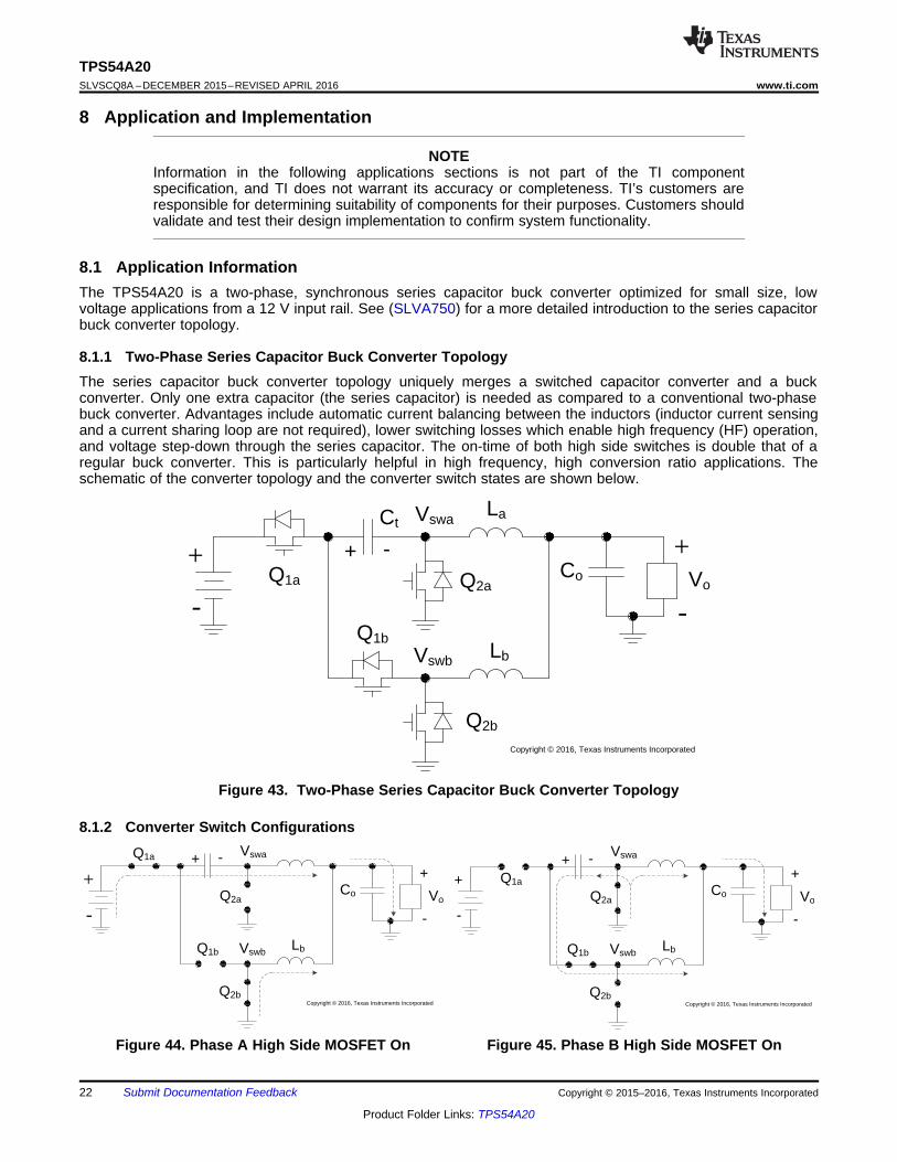
8.1.1 Two-Phase Series Capacitor Buck Converter TopologyThe series capacitor buck converter topology uniquely merges a switched capacitor converter and a buckconverter. Only one extra capacitor (the series capacitor) is needed as compared to a conventional two-phasebuck converter. Advantages include automatic current balancing between the inductors (inductor current sensingand a current sharing loop are not required), lower switching losses which enable high frequency (HF) operation,and voltage step-down through the series capacitor. The on-time of both high side switches is double that of aregular buck converter. This is particularly helpful in high frequency, high conversion ratio applications. Theschematic of the converter topology and the converter switch states are shown below.
Figure 43. Two-Phase Series Capacitor Buck Converter Topology
8.1.2 Converter Switch Configurations
Figure 44. Phase A High Side MOSFET On Figure 45. Phase B High Side MOSFET On
8.2.2.1 Output VoltageBefore beginning design, ensure that the series capacitor buck converter can be used in the application. It isrecommended to use this converter when the minimum input voltage is at least five times greater than the targetoutput voltage. If this recommendation is not followed, output voltage dropout can occur at heavy load conditionsand poor transient response to load increases can result.
The output voltage is set by connecting a resistor divider network from the output voltage to the FB pin of thedevice and to AGND. It is recommended that the lower divider resistor maintain a range between 1 kΩ and 10kΩ. To change the output voltage of a design, it is necessary to select the value of the upper resistor. The valueof RTOP for a specific output voltage can be calculated using Equation 2.
(2)
For the example design, 1 kΩ was selected for RBOT (R7). Using Equation 2, RTOP (R9) is calculated as 1.4 kΩ. Itis recommended to use resistors with ±1% or less variation.
A capacitor can be connected in parallel with the upper resistor to provide additional phase boost near theconverter's crossover frequency. See (SLVA289) for more details and design guidelines. For this design, 330 pFin series with 100 Ω is used. The values were optimized based on measured loop performance.
8.2.2.2 Switching FrequencyA key design step is to decide on a switching frequency for the regulator. There is a tradeoff between higher andlower switching frequencies. Higher switching frequencies may produce a smaller solution size using lowervalued inductors and smaller output capacitors compared to a power supply that switches at a lower frequency.However, the higher switching frequency creates extra switching loss, which reduces the converter’s efficiencyand thermal performance. In this design, a moderate switching frequency of 2 MHz per phase is selected toachieve both a small solution size and a high efficiency operation. Refer to Table 1 for the SS/FSELprogramming resistor selection.
8.2.2.3 On-TimeThe TON pin requires a resistor to set the nominal on-time and to support the input voltage feedforward circuit.The resistance value used also influences the internal ramp in the controller. As a starting point, Equation 3 isrecommended for selecting the TON resistor.
(3)
The RTON resistor (R5) is calculated to be 21 kΩ. The selected value for this design example is 22.1 kΩ. Duringstartup, the converter uses the nominal on-time programmed through TON. The phase lock loop (PLL) is onlyactivated after startup is complete. When the PLL is engaged, the on-time is adjusted. If the nominal on-timeprogrammed through the TON pin is not close to the on-time when the PLL is engaged, the SYNC range of thedevice may be reduced. The TON resistor can also be adjusted to tune the controller. Lowering the RTON valuewill increase the internal ramp height. This will reduce the converter’s sensitivity to noise and jitter but it will alsoreduce the transient response capabilities of the converter.
8.2.2.4 Inductor SelectionTo calculate the value of the output inductors, use Equation 4. KIND is a coefficient that represents the amount ofinductor ripple current relative to the maximum output current. The inductor ripple current is filtered by the outputcapacitor. In general, the inductor ripple value is at the discretion of the designer; however, KIND is normally from0.1 to 0.4 for the majority of applications.
(4)
For this design example, use KIND = 0.4 and the inductor value is calculated to be 249 nH. For this design, thenearby standard value of 220 nH was chosen. For the output filter inductor, it is generally recommended that theRMS current and saturation current ratings not be exceeded. The current ripple, RMS, and peak inductor currentare calculated in Equation 5, Equation 6, and Equation 7.
For this design, the RMS inductor current is calculated to be 5.04 A and the peak inductor current is 6.13 A. Thechosen inductor is 220 nH with a saturation current rating of 8.2 A and a dc current rating of 7.6 A.
The current flowing through each inductor is the inductor ripple current plus half the output current. During powerup, faults, or transient load conditions, the inductor current can increase above the peak inductor current levelcalculated above. In transient conditions, the inductor current can increase up to the switch current limit of thedevice. For this reason, the most conservative approach is to specify an inductor with a saturation current ratingequal to or greater than half the load current limit rather than the peak inductor current in steady state. Manyinductors today have soft saturation characteristics that may be able to ride through a transient that pushescurrent beyond the saturation rating specified in the datasheet. An example list of inductors that have beentested to work with the TPS54A20 are shown in Table 4. Inductors not listed below can also be used with thisdevice.
Table 4. Example Inductor List
Inductance (nH) Saturation CurrentRating (A)
Dimensions[L x W x H] (mm) DCR Typ/Max (mΩ) Type Vendor
220 ±20% 9.3 3.2 x 2.5 x 1.2 9 / 12 HMLW32251B-R22MS CYNTEC
330 ±20% 7.5 3.2 x 2.5 x 1.2 13 / 16 HMLW32251B-R33MS CYNTEC
220 ±30% 8.2 3.2 x 2.5 x 1.2 7.5 / 10.5 MLA-FY12NR22N-M3 MAGLAYERS
330 ±30% 7.5 3.2 x 2.5 x 1.2 13.5 / 16 MLA-FY12NR33N-M3 MAGLAYERS
220 ±20% 8.7 3.2 x 2.5 x 1.2 9.4 / 11.6 MCMK3225TR22MG TAIYO YUDEN
330 ±20% 10.4 3.2 x 2.5 x 1.2 11.2 / 13.8 MCMK3225TR33MG TAIYO YUDEN
250 ±30% 12 3.2 x 2.5 x 1.5 10 / 12.5 74479290125 WURTH ELECTRONIK
330 ±30% 12.4 4.1 x 4.1 x 2.1 6 / 7.2 744383560033 WURTH ELECTRONIK
220 ±20% 10.1 3.5 x 3.2 x 1.5 7.8 / 8.9 XEL3515-221 COILCRAFT
350 ±20% 8.2 3.5 x 3.2 x 1.5 11.6 / 13.4 XEL3515-351 COILCRAFT
330 ±20% 8.5 2.5 x 2.0 x 1.2 14 / 19 DFE252012F-R33M TOKO
8.2.2.5 Output Capacitor SelectionFor most applications, the primary consideration for selecting the value of the output capacitor is how theregulator responds to a large change in load current. The output capacitance may also be selected based onoutput voltage ripple or closed-loop bandwidth design objectives.
The output capacitance required to maintain an output voltage ripple ΔVOUT during steady-state operation can beestimated using Equation 8.
(8)
The desired response to a large change in the load current is typically the most stringent criteria. The outputcapacitor needs to supply the load with current when the regulator cannot. This situation would occur if there aredesired hold-up times for the regulator where the output capacitor must hold the output voltage above a certainlevel for a specified amount of time after the input power is removed. The regulator is also temporarily not able tosupply sufficient output current if there is a large, fast change in the load current such as a transition from noload to full load. The output capacitor must be sized to supply the extra current to the load until the control loopresponds to the load change. The minimum output capacitance required for a load increase can be estimatedusing Equation 9.
In low voltage applications, the inductor slew rate during a load step decrease is sometimes slower than its slewrate during a load step increase. The minimum output capacitance required for a load decrease can be estimatedusing Equation 10 for a given tolerable amount of overshoot in the output voltage.
(10)
Here ΔIOUT is the change in output current and ΔVOUT is the allowable change in the output voltage. For thisdesign example, the transient load response is specified as a 3% change in VOUT for a load step of 5A. For thisexample, ΔIOUT = 5 A and ΔVOUT = 0.03 x 1.2 = 0.036 V. Based on these design parameters, a minimumcapacitance of 93 µF is calculated using Equation 9. This value does not take the ESR of the output capacitorinto account in the output voltage change. For ceramic capacitors, the ESR is usually small enough to ignore inthis calculation. Additional capacitance de-ratings for aging, temperature and DC bias should be factored inwhich also increases this minimum value. For this design example, two 47 µF, 6.3 V rated, ceramic capacitorswith 3 mΩ of ESR are selected.
8.2.2.6 Input Capacitor SelectionThe TPS54A20 requires a high quality ceramic, type X5R or X7R, input decoupling capacitor of at least 4.7 µF ofeffective capacitance on the VIN input voltage pin. Additional bulk capacitance may also be required for the VINinput. The value of a ceramic capacitor varies significantly over temperature and the amount of DC bias appliedto the capacitor. The capacitance variations due to temperature can be minimized by selecting a dielectricmaterial that is stable over temperature. X5R and X7R ceramic dielectrics are usually selected for powerregulator capacitors because they have a high capacitance to volume ratio and are fairly stable overtemperature. The capacitor must also be selected with the DC bias taken into account. The capacitance value ofa capacitor decreases as the DC bias across a capacitor increases. For this example design, a ceramic capacitorwith at least a 25-V voltage rating is selected to support the maximum input voltage. The input capacitance valueimpacts the input ripple voltage of the regulator. The minimum input capacitance can be estimated usingEquation 11.
(11)
Here ΔVIN is the input voltage ripple in steady state. Using the design example values, IOUT = 10 A, VOUT = 1.2 V,VIN(MIN) = 9 V, FSW = 2 MHz and ΔVIN = 25 mV, Equation 11 yields an input capacitance of 39 µF. For thisexample, two 10µF, 25-V and a single 22-µF, 25-V ceramic capacitors in parallel have been selected for the VINvoltage rail. Because ESR is typically fairly low in ceramic capacitors, it is not included in this calculation.
The capacitor must also have a ripple current rating greater than the maximum input current ripple to the deviceduring full load. The input ripple current can be calculated using Equation 12.
(12)
For this example design, the RMS input ripple current is 2.21 A (RMS). The ripple current can be assumed to beshared equally between the input capacitors.
8.2.2.7 Series Capacitor SelectionA major function of the series capacitor is energy transfer. This is a different role from input and output capacitorswhere decoupling is the primary function. In many ways, the series capacitor is similar to the capacitor used forenergy transfer in SEPIC converters and can be designed accordingly. A design objective may be to ensure theseries capacitor voltage ripple does not exceed 5% to 10% of the nominal voltage under the worst caseconditions. The series capacitor voltage ripple is given by Equation 13.
Here Ct is the series capacitance. Equation 13 can be rearranged to provide the design equation for seriescapacitor selection which is
(14)
where kCt represents the voltage ripple percentage. For example, if the voltage ripple target is 5%, the value forkCt is 0.05. The largest voltage ripple occurs at full load current (highest IOUT), highest duty ratio (lowest inputvoltage/highest output voltage), and lowest frequency. For this design example, the value for kCt was selected tobe 0.08. The resulting series capacitance calculated is 1.85 µF. A 10 V, X7R ceramic capacitor with 2.2 µF ofcapacitance is selected.
Another aspect to consider is capacitor RMS current rating. This impacts the temperature rise of the capacitor.Check the capacitor datasheet for temperature rise information. If the temperature rise is too large for a singlecapacitor, multiple capacitors may be placed in parallel to share the RMS current. The series capacitor has thesame current profile as the high side MOSFETs. The RMS current squared can be expressed as
(15)
where IL(RMS) is the RMS inductor current of either inductor. The series capacitor RMS current can be expressedas
(16)
where ΔIL is the inductor current ripple. The largest RMS current occurs at the highest load current and highestduty ratio.
Multilayer ceramic capacitors (MLCC) are well suited for operating as the series capacitor. The equivalent seriesresistance (ESR) is relatively low (for example, 5 mΩ to 10 mΩ) which helps to reduce power loss and selfheating. The equivalent series inductance (ESL) is fairly low which results in a high self resonant frequency(SRF). There are a few key items that should be considered when designing. First, the effective capacitancedecreases with DC bias. This means that the capacitor should be selected based on its capacitance with thenominal voltage of VIN/2 applied. Temperature variation also reduces effective capacitance. For this reason, X7Rcapacitors with up to 125°C operating temperature range are recommended. If capacitors are not properlyselected, cracking or other failure modes may result.
8.2.2.8 Soft-Start Time SelectionThe soft-start time is the amount of time it takes for the output voltage to reach its nominal programmed valueduring power up. This is useful if a load requires a controlled voltage slew rate. This is also used if the outputcapacitance is very large and would require large amounts of current to quickly charge the capacitor to thedesired output voltage level. The large currents necessary to charge the capacitor may make the TPS54A20reach the current limit and trigger a fault. Excessive current draw from the input power supply may cause theinput voltage rail to sag. Limiting the output voltage slew rate solves both of these problems. The soft-start timecan be selected using the resistor values listed in Table 1. For the example circuit, the soft-start time is notcritical since the output capacitor value is 94 µF which does not require a large amount of current to charge to1.2 V. For this example design, the average output current is approximately 220 mA during soft start. Theexample circuit has the soft start time set to 512 µs which requires no resistor (open connection) on the SS/FSELpin. The average converter output current required to charge the output capacitors to the target output voltageduring soft start can be estimated using Equation 17.
(17)
8.2.2.9 Bootstrap Capacitor SelectionA 0.047 μF ceramic capacitor should be connected between the BOOTA to SCAP pins and between the BOOTBand SWB pins for proper operation. It is recommended to use a ceramic capacitor with X5R or better gradedielectric. The capacitor should have 10 V or higher voltage rating.
8.2.2.10 Gate Drive Capacitor SelectionA 1 μF ceramic capacitor should be connected between VGA and PGND and between the VG+ and VG- pins forproper operation. It is recommended to use a ceramic capacitor with X5R or better grade dielectric. The VGAcapacitor should have 16 V or higher voltage rating and the VG+ capacitor should have 10 V or higher voltagerating.
8.2.2.11 Under Voltage Lockout Set PointThe Under Voltage Lock Out (UVLO) set point can be adjusted using an external voltage divider network. Thetop resistor is connected between VIN and the EN pin and bottom resistor is connected between EN and GND asshown in Figure 42. For the example design, the supply should turn on and start switching once the input voltageincreases above 9.4 V (UVLO start or enable). After the regulator starts switching, it should continue to do sountil the input voltage falls below 9.2 V (UVLO stop or disable). The resistor values for obtaining the desiredUVLO thresholds can be calculated using Equation 18 and Equation 19. REN,TOP, the top UVLO divider resistor,is calculated using Equation 18. REN,BOT, the bottom UVLO divider resistor, is calculated in Equation 19.
(18)
(19)
For the start and stop voltages specified the resistor value selected for REN,TOP (R2) is 80.6 kΩ and for REN,BOT(R3) is 12.4 kΩ.
8.2.2.12 Current Limit SelectionThe current limit can be selected using the ILIM pin. Refer to Table 2 for resistor selection information. It isrecommended to choose a current limit that is 1.5 times or more than the full load current expected in theapplication. This allows for margin in the inductor currents when responding to load transients and limitsnuisance trips.
Figure 60. Shut Down with VIN Figure 61. Shut Down with EN
9 Power Supply RecommendationsThe TPS54A20 is designed to operate from an input voltage supply range between 8V and 14V. This supplyvoltage must be well regulated. Power supplies must be well bypassed for proper electrical performance. Thisincludes a minimum of one 4.7μF (after de-rating) ceramic capacitor, type X5R or better, from VIN to PGND.Additional local ceramic bypass capacitance may be required in systems with small input ripple specifications, inaddition to bulk capacitance, if the TPS54A20 device is located more than a few inches away from its inputpower supply. In systems with an auxiliary power rail available, the power stage input, VIN, and the gate driverpower input, VG+, may operate from separate input supplies. See the recommendations in the Layout section forfurther explanation.
10.1 Layout Guidelines• Layout is a critical portion of good power supply design. See Figure 62 and Figure 63 for a PCB layout
example. It may be possible to obtain acceptable performance with alternate PCB layouts, however thislayout has been shown to produce good results and is meant as a guideline.
• The IC package design provides several quiet pads for heat removal and enables a tight layout of the boardcomponents.
• Place the power components (including input and output capacitors, inductors, the series capacitor, and theTPS54A20 device) on the solder side of the PCB. To shield and isolate the small signal traces from noisypower lines, insert and connect at least one inner plane to ground.
• All sensitive analog traces and components such as FB, EN, TON, PGOOD, ILIM, and SS/FSEL must beplaced away from high-voltage switching nodes such as SWA, SWB, SCAP, BOOTA, and BOOTB to avoidcoupling. Use internal layers as ground planes and shield the feedback trace from power traces andcomponents.
• Care should be taken to minimize the loop area formed by the input bypass capacitor connections, the VINpin, and the ground connections. Place the input capacitors right next to the IC. Use low ESR ceramiccapacitors with X5R or X7R dielectric.
• Care should also be taken to minimize the loop area formed by the series capacitor. Place the seriescapacitor directly beside the IC. If this guideline is not followed, extra voltage ringing due to parasiticinductances could occur on the switch nodes and the device could be damaged. Use low ESR ceramiccapacitors with X7R or better dielectric. Ensure the capacitor operating temperature is sufficient. It isrecommended to have at least 125 °C rating.
• Place the bootstrap capacitors close to the device to reduce parasitic inductance caused by switching looparea. Place the BOOTA to SCAP capacitor right next to the device.
• Thermal vias should be inserted in the PGND strip and connected to internal ground planes. This aids withheat removal and ground return current.
• The top layer ground area should be connected to the internal ground layer(s) using vias at the input bypasscapacitor, the output filter capacitor and directly under the TPS54A20 device to provide a thermal path fromthe exposed thermal pad land to ground.
• For operation at full rated load, the top side ground area together with the internal ground planes, mustprovide adequate heat dissipating area.
• Place the output inductors close to the SWA and SWB pins and keep the switch node area small. This helpsto prevent excessive capacitive coupling, reduce electromagnetic interference, and reduce conduction loss.
• The output filter capacitor ground should be returned directly to the PGND strip using an inner layer.• The FB pin is sensitive to noise. The feedback resistors should be located as close as possible to the IC and
routed with minimal lengths of trace. Place the feedback resistor network near the device to minimize the FBtrace distance. When operating at 7 MHz or 10 MHz, a resistor (e.g. 10 kΩ) is required in series with the FBpin to reduce noise coupling and filter out high frequency noise as shown in Figure 62.
• Adding a phase boost capacitor in parallel with the top resistor of the output voltage feedback divider isrecommended.
• Place the TON resistor directly next to the device. Connect the ground return to the AGND pin.• Place the gate drive capacitor as close as possible to the VG+ and VG- pins. Make the return connection
directly to the VG- pin instead of an inner ground layer. This reduces gate drive loop area.• Place the VGA capacitor next to the VGA pin. Provide a ground via for the capacitor and ensure the loop is
as small as possible.• The no connect (NC) pin should be connected to the trace connecting the SCAP pin to the series capacitor.
This will improve board level reliability.• A snubber can be placed between the switch nodes and ground for effective ringing reduction.• Land pattern and stencil information is provided in the data sheet addendum.• Try to minimize conductor lengths while maintaining adequate width.• It is recommended to experimentally validate all designs before production.
Introduction to the Series Capacitor Buck Converter, SLVA750.
11.2 Community ResourcesThe following links connect to TI community resources. Linked contents are provided "AS IS" by the respectivecontributors. They do not constitute TI specifications and do not necessarily reflect TI's views; see TI's Terms ofUse.
TI E2E™ Online Community TI's Engineer-to-Engineer (E2E) Community. Created to foster collaborationamong engineers. At e2e.ti.com, you can ask questions, share knowledge, explore ideas and helpsolve problems with fellow engineers.
Design Support TI's Design Support Quickly find helpful E2E forums along with design support tools andcontact information for technical support.
11.3 TrademarksSWIFT, E2E are trademarks of Texas Instruments.
11.4 Electrostatic Discharge CautionThese devices have limited built-in ESD protection. The leads should be shorted together or the device placed in conductive foamduring storage or handling to prevent electrostatic damage to the MOS gates.
11.5 GlossarySLYZ022 — TI Glossary.
This glossary lists and explains terms, acronyms, and definitions.
12 Mechanical, Packaging, and Orderable InformationThe following pages include mechanical, packaging, and orderable information. This information is the mostcurrent data available for the designated devices. This data is subject to change without notice and revision ofthis document. For browser-based versions of this data sheet, refer to the left-hand navigation.
TPS54A20RNJR ACTIVE VQFN-HR RNJ 20 3000 Green (RoHS& no Sb/Br)
CU NIPDAU Level-2-260C-1 YEAR -40 to 125 54A20
TPS54A20RNJT ACTIVE VQFN-HR RNJ 20 250 Green (RoHS& no Sb/Br)
CU NIPDAU Level-2-260C-1 YEAR -40 to 125 54A20
(1) The marketing status values are defined as follows:ACTIVE: Product device recommended for new designs.LIFEBUY: TI has announced that the device will be discontinued, and a lifetime-buy period is in effect.NRND: Not recommended for new designs. Device is in production to support existing customers, but TI does not recommend using this part in a new design.PREVIEW: Device has been announced but is not in production. Samples may or may not be available.OBSOLETE: TI has discontinued the production of the device.
(2) Eco Plan - The planned eco-friendly classification: Pb-Free (RoHS), Pb-Free (RoHS Exempt), or Green (RoHS & no Sb/Br) - please check http://www.ti.com/productcontent for the latest availabilityinformation and additional product content details.TBD: The Pb-Free/Green conversion plan has not been defined.Pb-Free (RoHS): TI's terms "Lead-Free" or "Pb-Free" mean semiconductor products that are compatible with the current RoHS requirements for all 6 substances, including the requirement thatlead not exceed 0.1% by weight in homogeneous materials. Where designed to be soldered at high temperatures, TI Pb-Free products are suitable for use in specified lead-free processes.Pb-Free (RoHS Exempt): This component has a RoHS exemption for either 1) lead-based flip-chip solder bumps used between the die and package, or 2) lead-based die adhesive used betweenthe die and leadframe. The component is otherwise considered Pb-Free (RoHS compatible) as defined above.Green (RoHS & no Sb/Br): TI defines "Green" to mean Pb-Free (RoHS compatible), and free of Bromine (Br) and Antimony (Sb) based flame retardants (Br or Sb do not exceed 0.1% by weightin homogeneous material)
(3) MSL, Peak Temp. - The Moisture Sensitivity Level rating according to the JEDEC industry standard classifications, and peak solder temperature.
(4) There may be additional marking, which relates to the logo, the lot trace code information, or the environmental category on the device.
(5) Multiple Device Markings will be inside parentheses. Only one Device Marking contained in parentheses and separated by a "~" will appear on a device. If a line is indented then it is a continuationof the previous line and the two combined represent the entire Device Marking for that device.
(6) Lead/Ball Finish - Orderable Devices may have multiple material finish options. Finish options are separated by a vertical ruled line. Lead/Ball Finish values may wrap to two lines if the finishvalue exceeds the maximum column width.
Important Information and Disclaimer:The information provided on this page represents TI's knowledge and belief as of the date that it is provided. TI bases its knowledge and belief on informationprovided by third parties, and makes no representation or warranty as to the accuracy of such information. Efforts are underway to better integrate information from third parties. TI has taken andcontinues to take reasonable steps to provide representative and accurate information but may not have conducted destructive testing or chemical analysis on incoming materials and chemicals.TI and TI suppliers consider certain information to be proprietary, and thus CAS numbers and other limited information may not be available for release.
In no event shall TI's liability arising out of such information exceed the total purchase price of the TI part(s) at issue in this document sold by TI to Customer on an annual basis.
VQFN - 1 mm max heightRNJ0020APLASTIC QUAD FLATPACK - NO LEAD
PIN 1 INDEX AREA
SEATING PLANE
0.08 C
1
4
5
20
0.1 C B A0.05 C
10
11
13
PKG
14
12
19
ALL PADS
NOTES: 1. All linear dimensions are in millimeters. Any dimensions in parenthesis are for reference only. Dimensioning and tolerancing per ASME Y14.5M. 2. This drawing is subject to change without notice.
SCALE 3.200
www.ti.com
EXAMPLE BOARD LAYOUT
.000 PKG 0.000 PKG 0
.000
PK
G
0
4X ()
1.35
.000
PK
G
0
0.05 MINALL AROUND
0.05 MAXALL AROUND
8X(0.25)
8X (0.6)
(R0.05) TYP
()
1.12
5
()
1.1
()
1.07
5
()
1.12X
()
1.02
5
()
1.55
()
0.40
5
()
1.75
2X ( )1.11
( )0.395( )0.416
( )1.02
( )1.071
( )1.09
( )0.3845
4X ( )1.875
6X (0.5)
4X (0.65)
4X (0.45)
(1.65)
2X (1.7)
(3.9)
(1.75)
(0.7)
(0.4)
2X (0.325)
(0.5)
(0.3)
(0.35)
(0.45)
(0.4)
(0.25)
( 0.2) VIATYP
(0.8)
8X ( )1.9
VQFN - 1 mm max heightRNJ0020APLASTIC QUAD FLATPACK - NO LEAD
4222378/C 04/2018
1
4
11
19
LAND PATTERN EXAMPLESCALE:20X
5 10
12
14
2
3
13
20
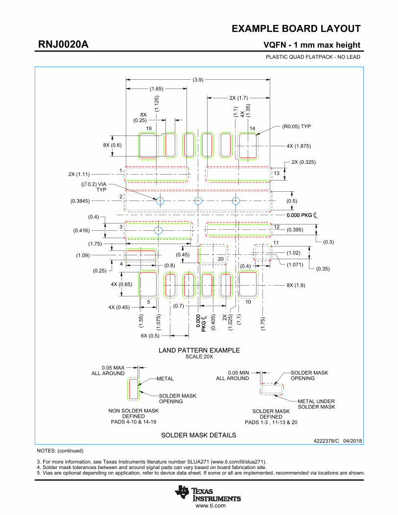
NOTES: (continued) 3. For more information, see Texas Instruments literature number SLUA271 (www.ti.com/lit/slua271).4. Solder mask tolerances between and around signal pads can vary based on board fabrication site.5. Vias are optional depending on application, refer to device data sheet. If some or all are implemented, recommended via locations are shown.
METAL
SOLDER MASKOPENING
SOLDER MASK DETAILS
NON SOLDER MASKDEFINED
PADS 4-10 & 14-19
SOLDER MASKOPENING
METAL UNDERSOLDER MASK
SOLDER MASKDEFINED
PADS 1-3 , 11-13 & 20
www.ti.com
EXAMPLE STENCIL DESIGN
.000
PK
G
0
.000PKG
0
(R0.05) TYP
8X (0.6)
8X (0.25)
4X (0.65)
4X (0.4)
2X (0.725) 4X (0.75)
4X (0.825)
2X (0.775)
(0.4)
(0.65)
(0.8)
4X (0.325)
4X(0.5)
2X (0.4)
(0.25)
(0.43)
(0.35)
2X (0.3)
()
1.35
()
1.58
8
()
0.66
3
2X (
)0.
513
2X (
)1.
538
()
0.62
5
()
1.57
5
()
0.58
8
()
1.56
3
()
0.40
5
()
1.75
4X ( )1.875
4X ( )1.11
4X ( )0.3845
2X ( )0.416
( )1.09
2X ( )0.395
( )1.02( )1.071
8X ( )PADS 6-9& 15-18
1.9
()
1.55
6X (0.5)
()
0.62
5
()
1.57
5
4222378/C 04/2018
VQFN - 1 mm max heightRNJ0020APLASTIC QUAD FLATPACK - NO LEAD
NOTES: (continued) 6. For alternate stencil design recommendations, see IPC-7525 or board assembly site preference.
4
5 10
11
13
14
20
SOLDER PASTE EXAMPLEBASED ON 0.125 mm THICK STENCIL
PRINTED SOLDER COVERAGE BY AREA
PAD 1: 86%, PAD 2: 83%, PADS 3, 12 & 13: 87%, PADS 5,10,14,19 & 20: 89%SCALE:30X
SOLDER MASKEDGE, TYP
2XEXPOSED METAL
METAL UNDERSOLDER MASKTYP
1
2
3
12
19
7XEXPLOSEDMETAL
8XEXPOSEDMETAL
6
15
IMPORTANT NOTICE
Texas Instruments Incorporated (TI) reserves the right to make corrections, enhancements, improvements and other changes to itssemiconductor products and services per JESD46, latest issue, and to discontinue any product or service per JESD48, latest issue. Buyersshould obtain the latest relevant information before placing orders and should verify that such information is current and complete.TI’s published terms of sale for semiconductor products (http://www.ti.com/sc/docs/stdterms.htm) apply to the sale of packaged integratedcircuit products that TI has qualified and released to market. Additional terms may apply to the use or sale of other types of TI products andservices.Reproduction of significant portions of TI information in TI data sheets is permissible only if reproduction is without alteration and isaccompanied by all associated warranties, conditions, limitations, and notices. TI is not responsible or liable for such reproduceddocumentation. Information of third parties may be subject to additional restrictions. Resale of TI products or services with statementsdifferent from or beyond the parameters stated by TI for that product or service voids all express and any implied warranties for theassociated TI product or service and is an unfair and deceptive business practice. TI is not responsible or liable for any such statements.Buyers and others who are developing systems that incorporate TI products (collectively, “Designers”) understand and agree that Designersremain responsible for using their independent analysis, evaluation and judgment in designing their applications and that Designers havefull and exclusive responsibility to assure the safety of Designers' applications and compliance of their applications (and of all TI productsused in or for Designers’ applications) with all applicable regulations, laws and other applicable requirements. Designer represents that, withrespect to their applications, Designer has all the necessary expertise to create and implement safeguards that (1) anticipate dangerousconsequences of failures, (2) monitor failures and their consequences, and (3) lessen the likelihood of failures that might cause harm andtake appropriate actions. Designer agrees that prior to using or distributing any applications that include TI products, Designer willthoroughly test such applications and the functionality of such TI products as used in such applications.TI’s provision of technical, application or other design advice, quality characterization, reliability data or other services or information,including, but not limited to, reference designs and materials relating to evaluation modules, (collectively, “TI Resources”) are intended toassist designers who are developing applications that incorporate TI products; by downloading, accessing or using TI Resources in anyway, Designer (individually or, if Designer is acting on behalf of a company, Designer’s company) agrees to use any particular TI Resourcesolely for this purpose and subject to the terms of this Notice.TI’s provision of TI Resources does not expand or otherwise alter TI’s applicable published warranties or warranty disclaimers for TIproducts, and no additional obligations or liabilities arise from TI providing such TI Resources. TI reserves the right to make corrections,enhancements, improvements and other changes to its TI Resources. TI has not conducted any testing other than that specificallydescribed in the published documentation for a particular TI Resource.Designer is authorized to use, copy and modify any individual TI Resource only in connection with the development of applications thatinclude the TI product(s) identified in such TI Resource. NO OTHER LICENSE, EXPRESS OR IMPLIED, BY ESTOPPEL OR OTHERWISETO ANY OTHER TI INTELLECTUAL PROPERTY RIGHT, AND NO LICENSE TO ANY TECHNOLOGY OR INTELLECTUAL PROPERTYRIGHT OF TI OR ANY THIRD PARTY IS GRANTED HEREIN, including but not limited to any patent right, copyright, mask work right, orother intellectual property right relating to any combination, machine, or process in which TI products or services are used. Informationregarding or referencing third-party products or services does not constitute a license to use such products or services, or a warranty orendorsement thereof. Use of TI Resources may require a license from a third party under the patents or other intellectual property of thethird party, or a license from TI under the patents or other intellectual property of TI.TI RESOURCES ARE PROVIDED “AS IS” AND WITH ALL FAULTS. TI DISCLAIMS ALL OTHER WARRANTIES ORREPRESENTATIONS, EXPRESS OR IMPLIED, REGARDING RESOURCES OR USE THEREOF, INCLUDING BUT NOT LIMITED TOACCURACY OR COMPLETENESS, TITLE, ANY EPIDEMIC FAILURE WARRANTY AND ANY IMPLIED WARRANTIES OFMERCHANTABILITY, FITNESS FOR A PARTICULAR PURPOSE, AND NON-INFRINGEMENT OF ANY THIRD PARTY INTELLECTUALPROPERTY RIGHTS. TI SHALL NOT BE LIABLE FOR AND SHALL NOT DEFEND OR INDEMNIFY DESIGNER AGAINST ANY CLAIM,INCLUDING BUT NOT LIMITED TO ANY INFRINGEMENT CLAIM THAT RELATES TO OR IS BASED ON ANY COMBINATION OFPRODUCTS EVEN IF DESCRIBED IN TI RESOURCES OR OTHERWISE. IN NO EVENT SHALL TI BE LIABLE FOR ANY ACTUAL,DIRECT, SPECIAL, COLLATERAL, INDIRECT, PUNITIVE, INCIDENTAL, CONSEQUENTIAL OR EXEMPLARY DAMAGES INCONNECTION WITH OR ARISING OUT OF TI RESOURCES OR USE THEREOF, AND REGARDLESS OF WHETHER TI HAS BEENADVISED OF THE POSSIBILITY OF SUCH DAMAGES.Unless TI has explicitly designated an individual product as meeting the requirements of a particular industry standard (e.g., ISO/TS 16949and ISO 26262), TI is not responsible for any failure to meet such industry standard requirements.Where TI specifically promotes products as facilitating functional safety or as compliant with industry functional safety standards, suchproducts are intended to help enable customers to design and create their own applications that meet applicable functional safety standardsand requirements. Using products in an application does not by itself establish any safety features in the application. Designers mustensure compliance with safety-related requirements and standards applicable to their applications. Designer may not use any TI products inlife-critical medical equipment unless authorized officers of the parties have executed a special contract specifically governing such use.Life-critical medical equipment is medical equipment where failure of such equipment would cause serious bodily injury or death (e.g., lifesupport, pacemakers, defibrillators, heart pumps, neurostimulators, and implantables). Such equipment includes, without limitation, allmedical devices identified by the U.S. Food and Drug Administration as Class III devices and equivalent classifications outside the U.S.TI may expressly designate certain products as completing a particular qualification (e.g., Q100, Military Grade, or Enhanced Product).Designers agree that it has the necessary expertise to select the product with the appropriate qualification designation for their applicationsand that proper product selection is at Designers’ own risk. Designers are solely responsible for compliance with all legal and regulatoryrequirements in connection with such selection.Designer will fully indemnify TI and its representatives against any damages, costs, losses, and/or liabilities arising out of Designer’s non-compliance with the terms and provisions of this Notice.