TPS62480 SW1 SW2 VO FB RS SS/TR AGND PGND VIN1 VIN2 EN MODE VSEL TG PG 470nH 470nH 2.4 to 5.5 V VOUT/6A R2 R1 4x 22uF 22uF R3 3.3nF 22uF Product Folder Sample & Buy Technical Documents Tools & Software Support & Community An IMPORTANT NOTICE at the end of this data sheet addresses availability, warranty, changes, use in safety-critical applications, intellectual property matters and other important disclaimers. PRODUCTION DATA. TPS62480 SLVSCL9A – FEBRUARY 2016 – REVISED FEBRUARY 2016 TPS62480 2.4-V to 5.5-V, 6-A, 2-Phase Step-Down Converter 1 1 Features 1• Dual Phase Current Mode Topology • Input Voltage Range 2.4 to 5.5 V • Output Voltage Range 0.6 to 5.5 V • Output Current of 6 A • Typical Quiescent Current of 23 μA • Feedback Voltage Accuracy of ±1% (PWM Mode) • Output Voltage Select • Phase Shifted Operation • Automatic Power Save Modes • Forced PWM Mode • Adjustable Soft Start • Power Good / Thermal Good Outputs • Undervoltage Lockout • Overcurrent and Short-Circuit Protection • Overtemperature Protection • 3 × 2.5 mm HotRod™ Package 2 Applications • Low Profile Point-of-Load Supply • Solid State Drives • Ultra Portable/Tablet/Embedded PC • Optical Modules, CMOS Cameras • Wireless Modules, Network Cards 3 Description The TPS62480 is a synchronous 2-phase step-down DC-DC converter for low profile point-of-load power supplies. The input voltage range of 2.4 to 5.5 V enables operation from typical 3.3-V or 5-V interface supplies as well as from backup circuits dropping down as low as 2.4 V. The output current is up to 6 A continuously provided by two phases of 3 A each, allowing the use of low-profile external components. Both the rails are running out of phase, reducing pulse current noise significantly. The TPS62480 provides an automatically entered power save mode to maintain high efficiency down to very light loads. This incorporates an automatic phase adding and shedding feature using both or only one phase according to the actual load. The device features a Power Good signal and an adjustable soft start. Also, the device features a Thermal Good signal to detect excessive internal temperature. The output voltage can be changed to a preselected value by VSEL pin. TPS62480 is able to operate in 100% duty cycle mode. The TPS62480 is packaged in a small 3 × 2.5 mm HotRod™ package (RNC). Device Information (1) PART NUMBER PACKAGE BODY SIZE (NOM) TPS62480 VQFN (16) 3.00 × 2.50 mm (1) For all available packages, see the orderable addendum at the end of the data sheet. space Typical Application Schematic Efficiency vs Output Current space
Transcript
TPS62480
SW1
SW2
VO
FB
RS
SS/TR
AGND
PGND
VIN1
VIN2
EN
MODE
VSEL
TG
PG
470nH
470nH
2.4 to 5.5 V
VOUT/6A
R2
R1
4 x
22uF
22uF
R3
3.3nF
22uF
Product
Folder
Sample &Buy
Technical
Documents
Tools &
Software
Support &Community
An IMPORTANT NOTICE at the end of this data sheet addresses availability, warranty, changes, use in safety-critical applications,intellectual property matters and other important disclaimers. PRODUCTION DATA.
TPS62480SLVSCL9A –FEBRUARY 2016–REVISED FEBRUARY 2016
TPS62480 2.4-V to 5.5-V, 6-A, 2-Phase Step-Down Converter
1
1 Features1• Dual Phase Current Mode Topology• Input Voltage Range 2.4 to 5.5 V• Output Voltage Range 0.6 to 5.5 V• Output Current of 6 A• Typical Quiescent Current of 23 µA• Feedback Voltage Accuracy of ±1% (PWM Mode)• Output Voltage Select• Phase Shifted Operation• Automatic Power Save Modes• Forced PWM Mode• Adjustable Soft Start• Power Good / Thermal Good Outputs• Undervoltage Lockout• Overcurrent and Short-Circuit Protection• Overtemperature Protection• 3 × 2.5 mm HotRod™ Package
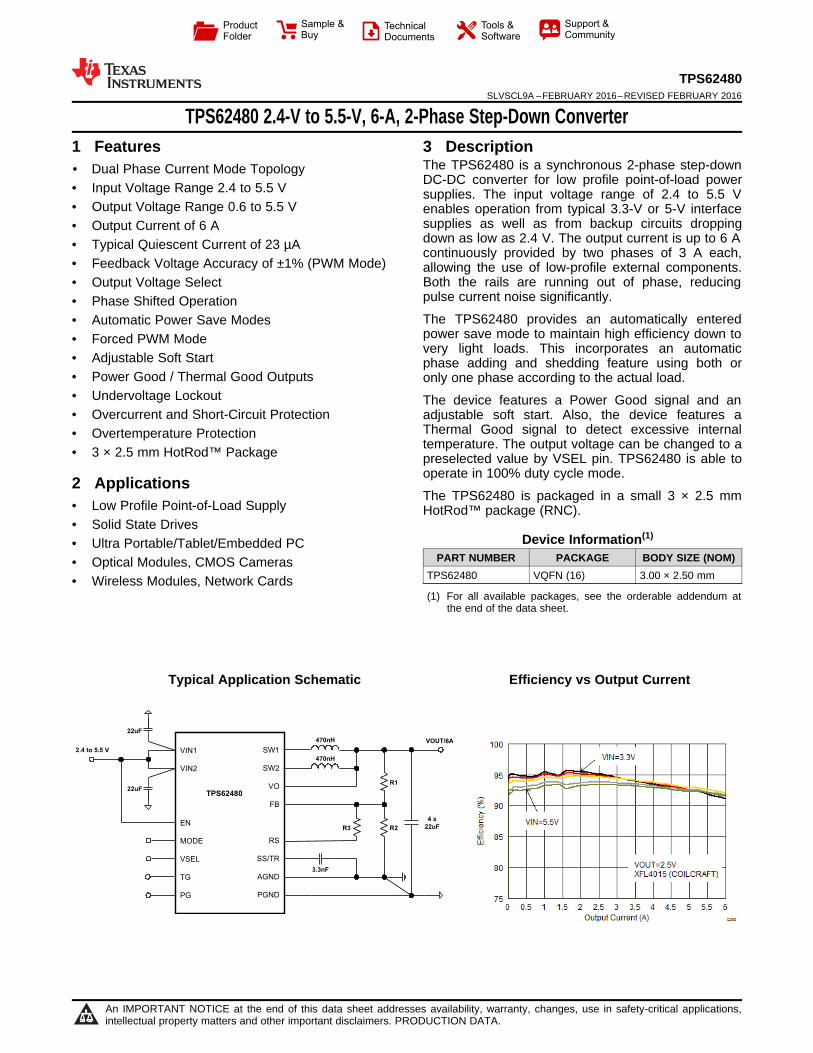
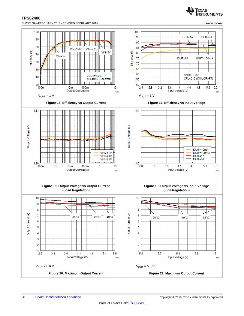
3 DescriptionThe TPS62480 is a synchronous 2-phase step-downDC-DC converter for low profile point-of-load powersupplies. The input voltage range of 2.4 to 5.5 Venables operation from typical 3.3-V or 5-V interfacesupplies as well as from backup circuits droppingdown as low as 2.4 V. The output current is up to 6 Acontinuously provided by two phases of 3 A each,allowing the use of low-profile external components.Both the rails are running out of phase, reducingpulse current noise significantly.
The TPS62480 provides an automatically enteredpower save mode to maintain high efficiency down tovery light loads. This incorporates an automaticphase adding and shedding feature using both oronly one phase according to the actual load.
The device features a Power Good signal and anadjustable soft start. Also, the device features aThermal Good signal to detect excessive internaltemperature. The output voltage can be changed to apreselected value by VSEL pin. TPS62480 is able tooperate in 100% duty cycle mode.
The TPS62480 is packaged in a small 3 × 2.5 mmHotRod™ package (RNC).
Device Information(1)
PART NUMBER PACKAGE BODY SIZE (NOM)TPS62480 VQFN (16) 3.00 × 2.50 mm
(1) For all available packages, see the orderable addendum atthe end of the data sheet.
space
Typical Application Schematic Efficiency vs Output Current
9 Power Supply Recommendations ...................... 2610 Layout................................................................... 27
10.1 Layout Guidelines ................................................. 2710.2 Layout Example .................................................... 27
11 Device and Documentation Support ................. 2811.1 Third-Party Products Disclaimer ........................... 2811.2 Community Resources.......................................... 2811.3 Trademarks ........................................................... 2811.4 Electrostatic Discharge Caution............................ 2811.5 Glossary ................................................................ 28
12 Mechanical, Packaging, and OrderableInformation ........................................................... 28
4 Revision History
Changes from Original (February 2016) to Revision A Page
• Changed RCN Package To: RNC Package in Pin Configuration and Functions................................................................... 3• Changed RCN 16 PINS To: RNC 16 PINS in the Thermal Information table ........................................................................ 4• Changed the Test Conditions for ISD Shutdown Current From: EN = Low (≤ 0.4 V) To: EN = Low (≤ 0.3 V) in the
Electrical Characteristics ........................................................................................................................................................ 5• Changed the VOUT Feedback Voltage Accuracy, MAX value From: 25% To: 2.5% in the Electrical Characteristics ............ 6• Changed TPS62480RCN To: TPS62480RNC in Table 1 .................................................................................................... 13
(1) Stresses beyond those listed under Absolute Maximum Ratings may cause permanent damage to the device. These are stress ratingsonly, which do not imply functional operation of the device at these or any other conditions beyond those indicated under RecommendedOperating Conditions. Exposure to absolute-maximum-rated conditions for extended periods may affect device reliability.
(2) All voltages are with respect to network ground terminal.
6 Specifications
6.1 Absolute Maximum Ratingsover operating free-air temperature range (unless otherwise noted) (1)
Power Good / Thermal Good Sink Current PG, TG 10 mAOperating Junction Temperature Range, TJ -40 150 °CStorage Temperature Range, Tstg -65 150 °C
(1) JEDEC document JEP155 states that 500-V HBM allows safe manufacturing with a standard ESD control process.(2) JEDEC document JEP157 states that 250-V CDM allows safe manufacturing with a standard ESD control process.
6.2 ESD RatingsVALUE UNIT
V(ESD) Electrostatic dischargeHuman body model (HBM), per ANSI/ESDA/JEDEC JS-001, all pins (1) ±1000
VCharged device model (CDM), per JEDEC specification JESD22-C101,all pins (2) ±500
6.3 Recommended Operating Conditionsover operating junction temperature range (unless otherwise noted)
MIN TYP MAX UNITSupply Voltage Range, VIN 2.4 5.5 VOutput Voltage Range, VOUT 0.6 5.5 VMaximum Output Current, IOUT 6 AOperating junction temperature, TJ –40 125 °C
(1) For more information about traditional and new thermal metrics, see the IC Package Thermal Metrics application report, SPRA953.(2) See the Layout section.
6.5 Electrical Characteristicsover operating junction temperature range (TJ = –40°C to 125°C) and VIN = 2.4 V to 5.5 V. Typical values at VIN = 3.6 V andTJ = 25°C (unless otherwise noted).
PARAMETER TEST CONDITIONS MIN TYP MAX UNITSUPPLY
VIN Input Voltage RangeVIN rising 2.6 5.5
VVIN falling 2.4 5.5
IQ Operating Quiescent Current
EN = High, VIN ≥ 3 V, IOUT = 0 mA, device notswitching,TJ = -40°C to +85°C
23 38 µA
100% Mode operation 3.5 6.5 mAISD Shutdown Current EN = Low (≤ 0.3 V), TJ = -40°C to +85°C 0.5 18.5 µA
Electrical Characteristics (continued)over operating junction temperature range (TJ = –40°C to 125°C) and VIN = 2.4 V to 5.5 V. Typical values at VIN = 3.6 V andTJ = 25°C (unless otherwise noted).
PARAMETER TEST CONDITIONS MIN TYP MAX UNIT
(1) The output voltage accuracy in Power Save Mode can be improved by increasing the output capacitor value, reducing the output voltageripple.
(2) For detailed information on output discharge see Active Output Discharge.
OUTPUTVREF Internal Reference Voltage 0.6 VILKG(FB) Input Leakage Current (FB)
EN = HighVFB = 0.6 V 1 65 nA
ILKG(RS) Input Leakage Current (RS) VSEL = Low, VRS = 0.6 V 1 65 nARRS Internal resistance (RS to GND) VSEL = High, IRS = 1 mA 10 50 ΩVOUT Output Voltage Range VIN ≥ VOUT 0.6 5.5 V
VOUT Feedback Voltage AccuracyPWM Mode,VIN ≥ VOUT + 1V
TJ = –20°C to 85°C -1% 1%
TJ = –40°C to 125°C -1.4% 1.3%
VOUT Feedback Voltage Accuracy Power Save Mode, L = 0.47 µH,COUT = 4 x 22 µF (1) -1.4% 2.5%
Output Discharge Current (2) EN = Low, VOUT = 2.5 V 120 mALoad Regulation VOUT = 1.8 V, PWM mode operation 0.02 %/A
7.1 OverviewThe TPS62480 is a high efficiency synchronous switched mode step-down converter based on a 2-phase peakcurrent control topology. It is designed for smallest solution size low-profile applications, converting a 2.4 V to 5.5V input voltage into a lower 0.6 V to 5.5 V output voltage. While an outer voltage loop sets the regulationthreshold for the inner current loop, based on the actual VOUT level, the inner current loop regulates to the actualpeak inductor current level for every switching cycle. The regulation network is internally compensated. While theON-time is determined by duty cycle, inductance and cycle peak current, the switching frequency of typically 2.2MHz is set by a predicted OFF-time. The device features a Power Save Mode (PSM) to keep the conversionefficiency high over the whole load current range.
The TPS62480 is a 2-phase converter, sharing the load among the phases. Identical in construction, the secondphase control is connected with an adaptive delay to the first phase. Both the phases use the same regulationthreshold and cycle-by-cycle peak current setpoint. This ensures a phase-shifted as well as current-balancedoperation. Using the advantages of the 2-phase topology, a 6-A continuous output current is provided with highperformance and as small as possible solution size.
7.3.1 Enable / Shutdown (EN)The device starts operation, when VIN is present and enable (EN) is set High. Since the boundary EN thresholdsare specified with 1.2 V for rising and 0.4 V for falling voltages, the typical vales are 0.85 V (rising) and 0.65 V(falling). The device is disabled by pulling EN Low. Leaving the EN pin floating is not recommended.
7.3.2 Soft Start (SS), Pre-biased OutputThe internal soft start circuit controls the output voltage slope during startup. This avoids excessive inrush currentand provides an adjustable controlled output-voltage rise time. The soft start also prevents unwanted voltagedrop from high impedance power sources or batteries.
When EN is set to start device operation, the device starts switching after a delay of typically 200 µs and VOUTrises with a slope, controlled by the external capacitor which is connected to the SS/TR pin (soft start). Leavingthe SS/TR pin floating or connecting to VIN provides internally set fastest startup with a soft start slope of about80us. See Application Curves for typical startup operation.
The device can start into a pre-biased output. In this case, the device starts switching, only when the internal setpoint for VOUT increases above the pre-biased voltage level.
7.3.3 Tracking (TR)The device tracks an external voltage applied to the SS/TR pin. The FB voltage tracks the external voltage aslong as it is below about 0.6V. Above 0.6V the device goes to normal operation. If the voltage at the SS/TR pindecreases below about 0.6V, the FB voltage tracks again this voltage. See Tracking for further details.
7.3.4 Output Voltage Select (VSEL)A resistive divider (VOUT to FB to AGND) sets the output voltage of the TPS62480. Providing a logic High levelat the VSEL pin, another resistor, connected between FB and RS pins is connected in parallel to the lowerresistor of the divider. This sets a different higher output voltage and can be used for dynamic voltage scaling(see Setting VOUT2 Using the VSEL Feature).
If the VSEL pin is set Low, the device connects an internal pull down resistor to keep the internal logic level Low,even if the pin is floating afterwards. The device disconnects the resistor, if the pin is set to High.
7.3.5 Forced PWM (MODE)To avoid Power Save Mode (PSM) Operation, the device can be forced to PWM mode operation by pulling theMODE pin High. In this case the device operates continuously with it's nominal switching frequency and theminimum peak current can go as low as -500 mA.
If the MODE pin is set Low, the device connects an internal pull down resistor to keep the internal logic levelLow, even if the pin is floating afterwards. The device disconnects the resistor, if the pin is set to High.
7.3.6 Power Good (PG)The TPS62480 has a built in power good function. The PG pin goes High, when the output voltage has reachedits nominal value. Otherwise, including when disabled, in UVLO or thermal shutdown, PG is Low. The PG pin isan open drain output that requires a pull-up resistor and can sink typically 2mA. If not used, the PG pin can beleft floating or grounded.
7.3.7 Thermal Good (TG)As long as the junction temperature of the TPS62480 is below the thermal good temperature of typically 120°C,the logic level at the TG pin is High. If the junction temperature exceeds that temperature, the TG pin goes Low.This can be used for the system to take action preventing excessive heating or even thermal shutdown. The TGpin is an open drain output that requires a pull-up resistor and can sink typically 2mA. If not used, the TG pin canbe left floating or grounded.
Feature Description (continued)7.3.8 Active Output DischargeThe VO pin, connected to the output voltage, provides an active discharge path when the device is switched offby setting EN Low or UVLO event. In case of being activated, this discharge circuit sinks typically 120mA foroutput voltages of typically 1 V and above. If VOUT is lower, the active current sink enters linear operation modeand the discharge current decreases.
7.3.9 Undervoltage Lockout (UVLO)The undervoltage lockout prevents misoperation of the device, if the input voltage drops below the UVLOthreshold which is set to typically 2.3 V. The converter starts operation again once the input voltage exceeds thethreshold by a hysteresis of typically 200 mV.
7.3.10 Thermal ShutdownThe junction temperature (TJ) of the device is monitored by an internal temperature sensor. If TJ exceeds 160°C(typical), the device goes in thermal shutdown with a hysteresis of about 10°C. Both the power FETs are turnedoff and the PG pin goes Low. Once TJ has decreased enough, the device resumes normal operation with SoftStart.
7.4 Device Functional Modes
7.4.1 Pulse Width Modulation (PWM) OperationThe TPS62480 is based on a predictive OFF-time peak current control topology, operating with PWM incontinuous conduction mode for heavier loads. The switching frequency is typically 2.2MHz. Both the master andfollower phase regulate to the same VOUT level, each with a separate current loop, using the same peak currentset point, cycle by cycle. This provides excellent peak current balancing, independent of inductor dc resistancematching. Since the follower phase operates with an adaptive delay to the master phase, phase shifted operationis always obtained. If the load current decreases, the device runs with the master phase only (see PhaseAdd/Shed and Current Balancing).
PWM only mode can be forced by pulling MODE pin High. If MODE is set Low, the device features an automatictransition into Power Save Mode, entered at light loads, running in discontinuous conduction mode (DCM).
7.4.2 Power Save Mode (PSM) OperationAs the load current decreases to half the ripple current, the converter enters Power Save Mode operation. DuringPSM, the converter operates with reduced switching frequency maintaining high conversion efficiency. PowerSave Mode is based on an adaptive peak current target, to keep output voltage ripple low. Since each pulseshifts VOUT up, a pause time happens until VOUT trips the internal VOUT_Low threshold again and the next pulsetakes place.
The switching frequency in PSM (one phase operation) calculates as:
Device Functional Modes (continued)7.4.3 Minimum Duty Cycle and 100% Mode OperationThe minimum on-time, which is typically 70ns, normally determines a limit on the minimum operating duty cycle.The calculation is:
space(2)
space
However, a frequency foldback lowers the switching frequency depending on the duty cycle and ensures properregulation for every duty cycle.
There is no limit towards maximum duty cycle. When the input voltage becomes close to the output voltage, thedevice enters automatically 100% duty cycle mode and both high-side FETs switch on as long as VOUT remainsbelow the regulation setpoint. In this case, the voltage drop across the high-side FETs and the inductorsdetermines the output voltage level. An estimate for the minimum input voltage to maintain output voltageregulation is:
space
(3)
space
In 100% duty cycle mode, the low-side FETs are switched off. The typical quiescent current in 100% mode is3.5 mA.
7.4.4 Phase Shifted OperationUsing an inherent benefit of the two-phase conversion, the two phases of TPS6248X run out of phase. For everyswitching cycle, the second phase is not allowed to turn on its high-side FET until the master phase has reachedits peak current value. This limits the input RMS current and corresponding switching noise.
7.4.5 Phase Add/Shed and Current BalancingWhen the load current is below the internal threshold, only the master phase operates. The second phaseactivates, if the load current exceeds the threshold of typically 1.7 A. The second phase powers off with ahysteresis of about 0.5 A, when the load current decreases.
Since the internal circuitry and layout matches both phase circuits, the peak currents balance with less than 15%deviation at heavy loads. This is independent of the inductor's tolerance. However, the maximum peak current,specified as High-Side MOSFET Current Limit in Electrical Characteristics is not exceeded at any time. Adetailed example about current balancing is given in Figure 28.
7.4.6 Current Limit and Short Circuit ProtectionEach phase has a separate integrated peak current limit. The dc values are specified in the ElectricalCharacteristics. While its minimum value limits the output current of the phase, the maximum number gives thecurrent that must be considered to flow in some operating case. At the peak current limit, the device provides itsmaximum output current.
However, if the current limit situation remains for 512 consecutive switching cycles, the peak current folds back toabout 1/3 of the regular limit. This limits the output power for over current and short circuit events. The foldbackcurrent limit is released to the normal one only if the load current has decreased as far as needed to undercutthe (foldback) peak current limit.
NOTEInformation in the following applications sections is not part of the TI componentspecification, and TI does not warrant its accuracy or completeness. TI’s customers areresponsible for determining suitability of components for their purposes. Customers shouldvalidate and test their design implementation to confirm system functionality.
space
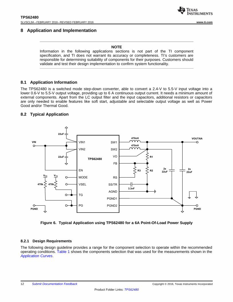
8.1 Application InformationThe TPS62480 is a switched mode step-down converter, able to convert a 2.4-V to 5.5-V input voltage into alower 0.6-V to 5.5-V output voltage, providing up to 6 A continuous output current. It needs a minimum amount ofexternal components. Apart from the LC output filter and the input capacitors, additional resistors or capacitorsare only needed to enable features like soft start, adjustable and selectable output voltage as well as PowerGood and/or Thermal Good.
8.2 Typical Applicationspace
space
Figure 6. Typical Application using TPS62480 for a 6A Point-Of-Load Power Supply
space
8.2.1 Design RequirementsThe following design guideline provides a range for the component selection to operate within the recommendedoperating conditions. Table 1 shows the components selection that was used for the measurements shown in theApplication Curves.
8.2.2.1 Setting the Adjustable Output VoltageWhile the device regulates the FB voltage to 0,6V, the output voltage is specified from 0.6 to 5.5 V. A resistivedivider (from VOUT to FB to AGND) sets the actual output voltage of the TPS62480. Equation 4 and Equation 5are calculating the values of the resistors. First, determining the current through the resistive divider leads to thetotal resistance (R1 + R2). A minimum divider current of about 5 µA is recommended and can be higher ifneeded.
space
(4)
(5)
space
8.2.2.2 Setting VOUT2 Using the VSEL FeatureA VOUT level, different as set with R1 and R2 (see Setting the Adjustable Output Voltage), can be forced byconnecting R3 between FB and RS pins and pulling VSEL High. R3 is calculated using Equation 6.
space
(6)
where:
V1 is the lower level output voltage and
V2 the higher level output voltage.
space
8.2.2.3 Output Filter SelectionThe TPS62480 is internally compensated and optimized to work for a certain range of L-C combinations. Therecommended minimum output capacitance is 4 x 22 µF, that can be ceramic capacitors exclusively. A largervalue of COUT might be needed for VOUT ≤ 1.8V, to improve transient response performance, as well as for VOUT> 3.3 V to compensate for voltage bias effects of the ceramic capacitors. The other way round, using of anadditional feed forward capacitor can help reducing amount of output capacitance that is needed to achieve acertain transient response target (see Output Capacitor Selection).
8.2.2.4 Inductor SelectionThe TPS62480 is designed to operate with two inductors of nominal 470 nH each. Inductors must be selected foradequate saturation current and for low dc resistance (DCR). The minimum inductor current rating IL(min) that isneeded under static load conditions calculates using Equation 7 and Equation 8. A current imbalance of 10% isincorporated.
space
(7)
space
(8)
space
Choosing VIN = 2 VOUT, this calculation provides the minimum saturation current of the inductor needed.Additional margin is recommended to cover dynamic overshoot due to load transients. For low profile solutions,the physical inductor size and the power losses have to be traded off. Smallest solution size gives less efficiencyand thermal performance due to larger DCR and/or core losses. The inductors shown in Table 2 have beentested with the TPS62480:
Table 2. List of Inductors
TYPEINDUCTANC
E [µH]CURRENT RATING MIN/TYP [A] DCR MAX
[mΩ]DIMENSIONS (LxBxH)
[mm] MANUFACTURERΔL/L = 30% ΔT = 40K
DFE201612E-R47M 0.47 ±20% 5.5/6.1 4.5/5.0 26 2.0 x 1.6 x 1.2 TOKO
DFE252012F-R47M 0.47 ±20% 6.7/7.4 4.9/5.8 22 2.5 x 2.0 x 1.2 TOKO
DFE252010F-R47M 0.47 ±20% 6.0/6.6 4.4/5.2 27 2.5 x 2.0 x 1.0 TOKO
HMLQ25201B-R47MSR-11 0.47 ±20% 5.6/6.2 4.2/4.7 28 2.5 x 2.0 x 1.2 CYNTEC
HMLQ20161T-R47MDR-11 0.47 ±20% 4.4/4.9 4.0/4.4 32 2.0 x 1.6 x 1.0 CYNTEC
GLCLMR4701A 0.47 ±20% 3.6/4.5 3.8/4.7 32 2.5 x 2.0 x 1.2 ALPS
GLCLKR4701A 0.47 ±20% 3.5/4.4 3.7/4.6 38 2.5 x 2.0 x 1.0 ALPS
XFL4015-471ME 0.47 ±20% 6.6 11.2 8.36 4.0 x 4.0 x 1.5 COILCRAFT
space
8.2.2.5 Output Capacitor SelectionThe TPS62480 provides a wide output voltage range of 0.6 V to 5.5 V. While stability is a critical criteria for theoutput filter selection, the output capacitor value also determines transient response behavior, ripple andaccuracy of VOUT. The internal compensation is designed for an output capacitance range from about 50 µF to150 µF effectively. Since ceramic capacitors are used preferably, this translates into nominal values of 4 x 22 µFto 4 x 47 µF and mainly depends on the output voltage. The following values are recommended:
(1) The values in the table are nominal values. The effective capacitance can differ significantly, depending on package size, voltage ratingand dielectric material.
space
Beyond the recommendations in Table 3, other values can be chosen and might be suitable depending on VOUTand actual effective capacitance. In such case, stability needs to be checked within the actual environment.
Even if the output capacitance is sufficient for stability, a different value might be desirable to improve thetransient response behavior. Table 4 can be used to determine capacitor values for specific transient responsetargets:
The architecture of the TPS62480 allows the use of tiny ceramic output capacitors with low equivalent seriesresistance (ESR). These capacitors provide low output voltage ripple and are recommended. To keep its lowresistance up to high frequencies and to get narrow capacitance variation with temperature, it is recommended touse X5R or X7R dielectrics. Using even higher values than demanded for stability and transient response hasfurther advantages like smaller voltage ripple and tighter dc output accuracy in Power Save Mode.
8.2.2.6 Input Capacitor SelectionThe input current of a buck converter is pulsating. Therefore, a low ESR input capacitor is required to preventlarge voltage transients at the source but to provide peak currents to the device. The recommended value formost applications is 2 x 22 µF, split between the VIN1 and VIN2 inputs and placed as close as possible to thesepins and PGND pins. If additional capacitance is needed, it can be added as bulk capacitance. To ensure properoperation, the effective capacitance at the VIN pins must not fall below 2 x 5 µF.
Low ESR multilayer ceramic capacitors are recommended for best filtering. Increasing with input voltage, the dcbias effect reduces the nominal capacitance value significantly. To decrease input ripple current further, largervalues of input capacitors can be used.
8.2.2.7 Soft Start Capacitor SelectionThe soft start ramp time can be set externally connecting a capacitor between the SS/TR and AGND pins. Thecapacitor value CSS that is needed to get a specific rising time ΔtSS calculates as:
space
(9)
space
Since the device has an internal delay time ΔtDELAY from EN=High to start switching, the overall startup time islonger as shown in Figure 7.
If very large output capacitances are used (e.g. >4x47µF), the use of a soft start capacitor is mandatory tosecure complete startup.
8.2.2.8 TrackingFor values up to 0.6V, an external voltage, connected to the SS/TR pin, drives the voltage level at the FB pin. Indoing so, the voltage at the FB pin is directly proportional to the voltage at the SS/TR pin.
When choosing the resistive divider proportion according to Equation 10, VOUT tracks VTR simultaneously.
space
(10)
space
Figure 8. Voltage Tracking
space
Following the example of Setting the Adjustable Output Voltage with VOUT = 1.8 V, R1 = 240 kΩ and R2 = 120kΩ, Equation 11 and Equation 12 calculate R3 and R4, connected to the SS/TR pin. Different to the resistivedivider at the FB pin, a larger current must be chosen, to avoid a tracking offset caused by the 5.25 µA currentthat flows out of the SS/TR pin. Assuming a 250 µA current, R4 calculates as follows:
However, the following limitations can influence the tracking accuracy:• The upper limit of the SS/TR voltage that can be tracked is about 0.6V. Since it is detected internally by a
comparator, process variation and ramp speed can cause up to ±30 mV different threshold.• In case that the voltage at SS/TR ramps up immediately when VIN is supplied or EN is set High, the internal
startup delay, ΔtDELAY, delays the ramp of VOUT. The internal ramp starts after ΔtDELAY at the voltage level,which is actually present at the SS/TR pin.
• The tracking down speed is limited by the RC time constant of the internal output discharge (alwaysconnected when tracking down) and the actual load with the output capacitance. Note: The device tracksdown with the same behavior for MODE High (Forced PWM) or Low (Auto PSM).
8.2.2.9 Current SharingThe TPS62480 is designed to share load current wisely between the 2 phases. The current imbalance is lessthan 15% over VIN and temperature range and independent on inductor mismatch.
However, the mismatch between the two inductors itself causes additional imbalance of the average inductorcurrents, caused by different ripple current. The mismatch can be calculated as shown in the following example,assuming that the nominal inductance of 470 nH can vary ±20%, the switching frequency is 2 MHz. Converting 5V into 2.5 V gives a duty cycle of 0.5, which effects maximum ripple current. Since the ripple current is calculatedwith:
space
(13)
space
the ripple currents in the two inductors are calculated with Iripple1 = 1.69 A and Iripple2 = 1.1 A which gives a ΔIrippleof 0.59 A as worst case number based on the maximum inductor tolerance. Figure 9 shows the relation of thetwo inductor currents in such case.
The difference in the average current is calculated using:
space
(14)
space
In this worst case calculation the average inductor current mismatch is 0.295A, less than 10% at the full loadcurrent of 3A per phase.
8.2.2.10 Thermal GoodThe Thermal Good pin provides an open drain output. The logic level is given by the pull up source which can beVOUT. In this case, TG goes or stays Low, when the device switches off due to EN, UVLO or ThermalShutdown.
When using an independent source for the pull up logic, the logic behavior at shutdown differs, because the TGpin internally goes high impedance. As before, TG goes Low when TG threshold is reached, but goes back Highin the event of being switched off (e.g. Thermal Shutdown).
Figure 44. A typical 1.2 V & 1.8 V, 6 A Power Supply
space
Figure 45. A typical 0.9 V & 1 V, 6 A Power Supply
space
9 Power Supply RecommendationsThe TPS62480 is designed to operate from a 2.4-V to 5.5-V input voltage supply. The input power supply'soutput current needs to be rated according to the output voltage and the output current of the power railapplication.
10.1 Layout GuidelinesA recommended PCB layout for the TPS62480 dual phase solution is shown below. It ensures best electrical andoptimized thermal performance considering the following important topics:
- The input capacitors must be placed as close as possible to the appropriate pins of the device. This provideslow resistive and inductive paths for the high di/dt input current. The input capacitance is split, as is the VINconnection, to avoid interference between the input lines.
- The SW node connection from the IC to the inductor conducts high currents. It should be kept short and can bedesigned in parallel with an internal or bottom layer plane, to provide low resistance and enhanced thermalbehavior.
- The VOUT regulation loop is closed with COUT and its ground connection. To avoid PGND noise crosstalk, PGNDis kept split for the regulation loop. If a ground layer or plane is used, a direct connection by vias, as shown, isrecommended. Otherwise the connection of COUT to GND must be short for good load regulation.
- The use of thermal (filled) vias underneath the device is recommended for improved thermal performance.
- The FB node is sensitive to dv/dt signals. Therefore the resistive divider should be placed close to the FB (andRS pin in case of using R3) pin, avoiding long trace distance.
For more detailed information about the actual 4 layer EVM solution, see SLVUAI6.
11.1 Third-Party Products DisclaimerTI'S PUBLICATION OF INFORMATION REGARDING THIRD-PARTY PRODUCTS OR SERVICES DOES NOTCONSTITUTE AN ENDORSEMENT REGARDING THE SUITABILITY OF SUCH PRODUCTS OR SERVICESOR A WARRANTY, REPRESENTATION OR ENDORSEMENT OF SUCH PRODUCTS OR SERVICES, EITHERALONE OR IN COMBINATION WITH ANY TI PRODUCT OR SERVICE.
11.2 Community ResourcesThe following links connect to TI community resources. Linked contents are provided "AS IS" by the respectivecontributors. They do not constitute TI specifications and do not necessarily reflect TI's views; see TI's Terms ofUse.
TI E2E™ Online Community TI's Engineer-to-Engineer (E2E) Community. Created to foster collaborationamong engineers. At e2e.ti.com, you can ask questions, share knowledge, explore ideas and helpsolve problems with fellow engineers.
Design Support TI's Design Support Quickly find helpful E2E forums along with design support tools andcontact information for technical support.
11.3 TrademarksHotRod, E2E are trademarks of Texas Instruments.
11.4 Electrostatic Discharge CautionThese devices have limited built-in ESD protection. The leads should be shorted together or the device placed in conductive foamduring storage or handling to prevent electrostatic damage to the MOS gates.
11.5 GlossarySLYZ022 — TI Glossary.
This glossary lists and explains terms, acronyms, and definitions.
12 Mechanical, Packaging, and Orderable InformationThe following pages include mechanical, packaging, and orderable information. This information is the mostcurrent data available for the designated devices. This data is subject to change without notice and revision ofthis document. For browser-based versions of this data sheet, refer to the left-hand navigation.
TPS62480RNCR ACTIVE VQFN-HR RNC 16 3000 RoHS & Green NIPDAU Level-1-260C-UNLIM -40 to 125 62480
TPS62480RNCT ACTIVE VQFN-HR RNC 16 250 RoHS & Green NIPDAU Level-1-260C-UNLIM -40 to 125 62480
(1) The marketing status values are defined as follows:ACTIVE: Product device recommended for new designs.LIFEBUY: TI has announced that the device will be discontinued, and a lifetime-buy period is in effect.NRND: Not recommended for new designs. Device is in production to support existing customers, but TI does not recommend using this part in a new design.PREVIEW: Device has been announced but is not in production. Samples may or may not be available.OBSOLETE: TI has discontinued the production of the device.
(2) RoHS: TI defines "RoHS" to mean semiconductor products that are compliant with the current EU RoHS requirements for all 10 RoHS substances, including the requirement that RoHS substancedo not exceed 0.1% by weight in homogeneous materials. Where designed to be soldered at high temperatures, "RoHS" products are suitable for use in specified lead-free processes. TI mayreference these types of products as "Pb-Free".RoHS Exempt: TI defines "RoHS Exempt" to mean products that contain lead but are compliant with EU RoHS pursuant to a specific EU RoHS exemption.Green: TI defines "Green" to mean the content of Chlorine (Cl) and Bromine (Br) based flame retardants meet JS709B low halogen requirements of <=1000ppm threshold. Antimony trioxide basedflame retardants must also meet the <=1000ppm threshold requirement.
(3) MSL, Peak Temp. - The Moisture Sensitivity Level rating according to the JEDEC industry standard classifications, and peak solder temperature.
(4) There may be additional marking, which relates to the logo, the lot trace code information, or the environmental category on the device.
(5) Multiple Device Markings will be inside parentheses. Only one Device Marking contained in parentheses and separated by a "~" will appear on a device. If a line is indented then it is a continuationof the previous line and the two combined represent the entire Device Marking for that device.
(6) Lead finish/Ball material - Orderable Devices may have multiple material finish options. Finish options are separated by a vertical ruled line. Lead finish/Ball material values may wrap to twolines if the finish value exceeds the maximum column width.
Important Information and Disclaimer:The information provided on this page represents TI's knowledge and belief as of the date that it is provided. TI bases its knowledge and belief on informationprovided by third parties, and makes no representation or warranty as to the accuracy of such information. Efforts are underway to better integrate information from third parties. TI has taken andcontinues to take reasonable steps to provide representative and accurate information but may not have conducted destructive testing or chemical analysis on incoming materials and chemicals.TI and TI suppliers consider certain information to be proprietary, and thus CAS numbers and other limited information may not be available for release.
In no event shall TI's liability arising out of such information exceed the total purchase price of the TI part(s) at issue in this document sold by TI to Customer on an annual basis.
VQFN - 1 mm max heightRNC0016APLASTIC QUAD FLATPACK - NO LEAD
4221751/A 02/2015
PIN 1 INDEX AREA
SEATING PLANE
0.08 C
1
3
4
160.1 C B A0.05 C
8
9
11
SYMM
SYMM
12
NOTES: 1. All linear dimensions are in millimeters. Any dimensions in parenthesis are for reference only. Dimensioning and tolerancing per ASME Y14.5M. 2. This drawing is subject to change without notice.
SCALE 4.000
www.ti.com
EXAMPLE BOARD LAYOUT
0.05 MINALL AROUND
0.05 MAXALL AROUND
10X (0.25)
(2.8)
10X (0.6)
4X (0.525)
6X (1.3)
6X (0.25)
8X (0.5)
(1.6)
(R ) TYP0.05
VQFN - 1 mm max heightRNC0016APLASTIC QUAD FLATPACK - NO LEAD
4221751/A 02/2015
SYMM
1
3
9
16
SYMM
LAND PATTERN EXAMPLESCALE:20X
4 8
11
12
NOTES: (continued) 3. For more information, see Texas Instruments literature number SLUA271 (www.ti.com/lit/slua271).4. Solder mask tolerances between and around signal pads can vary based on board fabrication site.
METAL
SOLDER MASKOPENING
SOLDER MASK DETAILS
NON SOLDER MASKDEFINED
PADS 4-8 & 12-16
SOLDER MASKOPENING
METAL UNDERSOLDER MASK
SOLDER MASKDEFINED
PADS 1-3 & 9-11
www.ti.com
EXAMPLE STENCIL DESIGN
(2.8)
10X (0.6)
10X (0.25)
6X (1.175)
12X (0.25)12X (0.55)
4X (0.525)
6X (0.425)
8X (0.5)
(R ) TYP0.05
VQFN - 1 mm max heightRNC0016APLASTIC QUAD FLATPACK - NO LEAD
4221751/A 02/2015
NOTES: (continued) 5. For alternate stencil design recommendations, see IPC-7525 or board assembly site preference.
SYMM
1
3
4 8
9
11
1216
SYMM
SOLDER PASTE EXAMPLEBASED ON 0.125 mm THICK STENCIL
FOR PADS 1-3 & 9-11
84.6% PRINTED SOLDER COVERAGE BY AREASCALE:30X
SOLDER MASKEDGE, TYP
6XEXPOSED METAL
METAL UNDERSOLDER MASKTYP
IMPORTANT NOTICE AND DISCLAIMER
TI PROVIDES TECHNICAL AND RELIABILITY DATA (INCLUDING DATASHEETS), DESIGN RESOURCES (INCLUDING REFERENCE DESIGNS), APPLICATION OR OTHER DESIGN ADVICE, WEB TOOLS, SAFETY INFORMATION, AND OTHER RESOURCES “AS IS” AND WITH ALL FAULTS, AND DISCLAIMS ALL WARRANTIES, EXPRESS AND IMPLIED, INCLUDING WITHOUT LIMITATION ANY IMPLIED WARRANTIES OF MERCHANTABILITY, FITNESS FOR A PARTICULAR PURPOSE OR NON-INFRINGEMENT OF THIRD PARTY INTELLECTUAL PROPERTY RIGHTS.These resources are intended for skilled developers designing with TI products. You are solely responsible for (1) selecting the appropriate TI products for your application, (2) designing, validating and testing your application, and (3) ensuring your application meets applicable standards, and any other safety, security, or other requirements. These resources are subject to change without notice. TI grants you permission to use these resources only for development of an application that uses the TI products described in the resource. Other reproduction and display of these resources is prohibited. No license is granted to any other TI intellectual property right or to any third party intellectual property right. TI disclaims responsibility for, and you will fully indemnify TI and its representatives against, any claims, damages, costs, losses, and liabilities arising out of your use of these resources.TI’s products are provided subject to TI’s Terms of Sale (www.ti.com/legal/termsofsale.html) or other applicable terms available either on ti.com or provided in conjunction with such TI products. TI’s provision of these resources does not expand or otherwise alter TI’s applicable warranties or warranty disclaimers for TI products.