TPS64200, TPS64201 TPS64202, TPS64203 SLVS485 - AUGUST 2003 SOT23 STEPĆDOWN CONTROLLER FEATURES D Step-Down Controller for Applications With up to 95% Efficiency D 1.8-V to 6.5-V Operating Input Voltage Range D Adjustable Output Voltage Range From 1.2 V to V I D High Efficiency Over a Wide Load Current Range D 100% Maximum Duty Cycle for Lowest Dropout D Internal Softstart D 20-µA Quiescent Current (Typical) D Overcurrent Protected D Available in a SOT23 Package APPLICATIONS D USB Powered Peripherals D Organizers, PDAs, and Handheld PCs D Low Power DSP Supply D Digital Cameras D Hard Disk Drives D Portable Audio Players DESCRIPTION The TPS6420x are nonsynchronous step-down controllers that are ideally suited for systems powered from a 5-V or 3.3-V bus or for applications powered from a 1-cell Li-Ion battery or from a 2- to 4-cell NiCd, NiMH, or alkaline battery. These step-down controllers drive an external P-channel MOSFET allowing design flexibility. To achieve highest efficiency over a wide load current range, this controller uses a minimum on time, minimum off time control scheme and consumes only 20-µA quiescent current. The minimum on time of typically 600 ns (TPS64203) allows the use of small inductors and capacitors. When disabled, the current consumption is reduced to less than 1 µA. The TPS6420x is available in the 6-pin SOT23 (DBV) package and operates over a free air temperature range of -40°C to 85°C. TYPICAL APPLICATION CIRCUIT 5 TPS64200 Si5447DC ZHCS2000 EN GND FB SW VIN ISENSE R s = 33 mΩ 10 µH 3.3 V / 2 A 47 µF PosCap 6TPA47M R1 620 kΩ R2 360 kΩ 10 µF 5 V 0 10 20 30 40 50 60 70 80 90 100 0.0001 0.001 0.01 0.1 1 10 T A = 25°C, V O = 3.3 V TPS64200 EFFICIENCY vs LOAD CURRENT I O - Load Current - A Efficiency - % V I = 4.2 V 1 2 3 6 4 PRODUCTION DATA information is current as of publication date. Products conform to specifications per the terms of Texas Instruments standard warranty. Production processing does not necessarily include testing of all parameters. Please be aware that an important notice concerning availability, standard warranty, and use in critical applications of Texas Instruments semiconductor products and disclaimers thereto appears at the end of this data sheet. www.ti.com Copyright 2003, Texas Instruments Incorporated
Transcript
SLVS485 − AUGUST 2003
FEATURES
Step-Down Controller for Applications Withup to 95% Efficiency
1.8-V to 6.5-V Operating Input Voltage Range
Adjustable Output Voltage Range From 1.2 Vto VI
High Efficiency Over a Wide Load CurrentRange
100% Maximum Duty Cycle for LowestDropout
Internal Softstart
20-µA Quiescent Current (Typical)
Overcurrent Protected
Available in a SOT23 Package
APPLICATIONS
USB Powered Peripherals
Organizers, PDAs, and Handheld PCs
Low Power DSP Supply
Digital Cameras
Hard Disk Drives
Portable Audio Players
DESCRIPTION
The TPS6420x are nonsynchronous step-downcontrollers that are ideally suited for systems poweredfrom a 5-V or 3.3-V bus or for applications powered froma 1-cell Li-Ion battery or from a 2- to 4-cell NiCd, NiMH, oralkaline battery. These step-down controllers drive anexternal P-channel MOSFET allowing design flexibility. Toachieve highest efficiency over a wide load current range,this controller uses a minimum on time, minimum off timecontrol scheme and consumes only 20-µA quiescentcurrent. The minimum on time of typically 600 ns(TPS64203) allows the use of small inductors andcapacitors. When disabled, the current consumption isreduced to less than 1 µA. The TPS6420x is available inthe 6-pin SOT23 (DBV) package and operates over a freeair temperature range of −40°C to 85°C.
Please be aware that an important notice concerning availability, standard warranty, and use in critical applications of Texas Instrumentssemiconductor products and disclaimers thereto appears at the end of this data sheet.
www.ti.com
Copyright 2003, Texas Instruments Incorporated
SLVS485 − AUGUST 2003
www.ti.com
2
These devices have limited built-in ESD protection. The leads should be shorted together or the device placed in conductive foam duringstorage or handling to prevent electrostatic damage to the MOS gates.
ORDERING INFORMATIONPLASTIC SOT23-6(1) (2)
(DBV)OUTPUT VOLTAGE MINIMUM ON-TIME MINIMUM OFF-TIME MARKING
TPS64200DBVRAdjustable1.2 V to VI
ON time = 1.6 µs OFF time = 600 ns PJAI
TPS64201DBVRAdjustable1.2 V to VI
Variable minimum on time OFF time = 600 ns PJBI
TPS64202DBVRAdjustable1.2 V to VI
Variable minimum on time OFF time = 300 ns PJCI
TPS64203DBVRAdjustable1.2 V to VI
ON time = 600 ns OFF time = 600 ns PJDI
(1) The R suffix indicates shipment in tape and reel with 3000 units per reel.(2) The T suffix indicates a mini reel with 250 units per reel.
ABSOLUTE MAXIMUM RATINGSover operating free-air temperature range unless otherwise noted(1)
Supply voltage, VIN −0.3 V to 7 V
Voltage at EN, SW, ISENSE −0.3 V to VIN
Voltage at FB −0.3 V to 3.3 V
Maximum junction temperature, TJ 150°C
Operating free−air temperature, TA −40°C to 85°C
Storage temperature, Tsgt −65°C to 150°C
Lead temperature 1,6 mm (1/16 inch) from case for 10 seconds 300°C
(1) Stresses beyond those listed under “absolute maximum ratings” may cause permanent damage to the device. These are stress ratings only, andfunctional operation of the device at these or any other conditions beyond those indicated under “recommended operating conditions” is notimplied. Exposure to absolute-maximum-rated conditions for extended periods may affect device reliability.
PACKAGE DISSIPATION RATINGS
PACKAGETA ≤25C
POWER RATINGDERATING FACTORABOVE TA = 25°C
TA = 70CPOWER RATING
TA = 85CPOWER RATING
SOT23−6 400 mW 4 mW/°C 220 mW 180 mW
NOTE: The thermal resistance junction to ambient of the 6−pin SOT23 package is 250°C/W.
RECOMMENDED OPERATING CONDITIONSMIN NOM MAX UNIT
Supply voltage at VIN 1.8 6.5 V
Operating junction temperature −40 125 °C
SLVS485 − AUGUST 2003
www.ti.com
3
ELECTRICAL CHARACTERISTICS VIN = 3.8 V, VO = 3.3 V, EN = VIN, TA = −40°C to 85°C (unless otherwise noted)
SUPPLY CURRENT
PARAMETER TEST CONDITIONS MIN TYP MAX UNIT
VI Input voltage range 1.8 6.5 V
I(Q) Operating quiescent current IO = 0 mA 20 35 µA
I(SD) Shutdown current EN = VI 0.1 1 µA
OUTPUT/CURRENT LIMIT
VO Adjustable output voltage range VFB VI V
VFB Feedback voltage 1.213 V
Feedback leakage current 0.01 0.2 µA
Feedback voltage tolerance −2 +2 %
V(ISENSE) Reference voltage for current limit 90 105 120 mV
ISENSE leakage current 0.01 0.2 µA
Line regulation Measured with circuit according to Figure 1 0.6 %/V
Load regulationMeasured with circuit according to Figure 1VI = 3.8 V
0.6 %/A
η Efficiency
Measured with circuit according to Figure 1VI = 3.8 V, VO = 3.3 V, IO = 1000 mA
94%
η EfficiencyMeasured with circuit according to Figure 1VI = 3.8 V, VO = 1.2 V, IO = 800 mA
80%
Start-up timeIO = 0 mA, Time from active EN to VO,CO = 47 µF
0.25 ms
GATE DRIVER (SW-PIN)
rDS(ON) P-channel MOSFET on-resistanceVI ≥ 2.5 V 4
ΩrDS(ON) P-channel MOSFET on-resistanceVI = 1.8 V 6
Ω
rDS(ON) N-channel MOSFET on-resistanceVI ≥ 2.5 V 4
ΩrDS(ON) N-channel MOSFET on-resistanceVI = 1.8 V 6
Ω
IO Maximum gate drive output current, SW 150 mA
ENABLE
VIH EN high level input voltage Device is off 1.3 V
VIL EN low level input voltage Device is operating 0.3 V
EN trip point hysteresis 115 mV
Ilkg EN input leakage current EN = GND or VIN 0.01 0.2 µA
V(UVLO) Undervoltage lockout threshold 1.7 V
ON TIME and OFF TIME
ton Minimum on timeTPS64200, TPS64201, TPS64202 1.36 1.6 1.84
ston Minimum on timeTPS64203 only 0.56 0.65 0.74
µs
Reduced on time 1 TPS64201,TPS64202 0.80 µs
Reduced on time 2 TPS64201,TPS64202 0.40 µs
Reduced on time 3 TPS64201,TPS64202 0.20 µs
toff Minimum off timeTPS64200,TPS64201, TPS64203 0.44 0.55 0.66
stoff Minimum off timeTPS64202 only 0.24 0.3 0.36
µs
SLVS485 − AUGUST 2003
www.ti.com
4
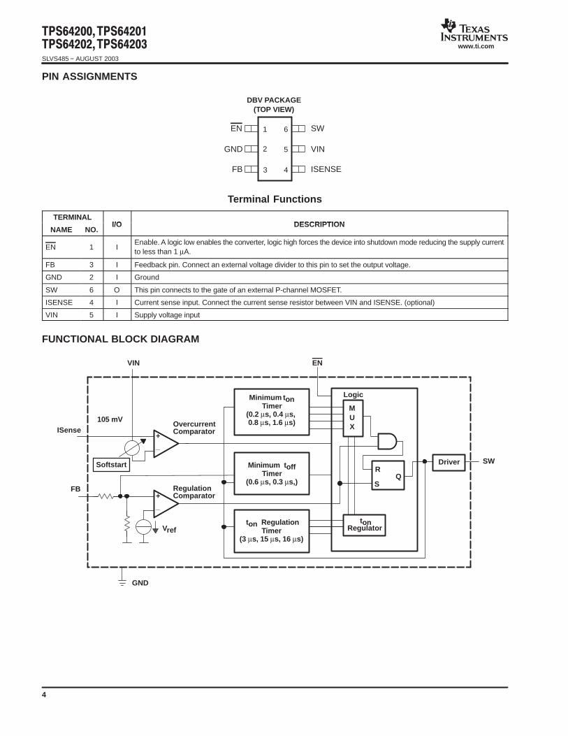
PIN ASSIGNMENTS
1
DBV PACKAGE(TOP VIEW)
EN
FB
VIN
3
5GND
SW
ISENSE
2
6
4
Terminal Functions
TERMINALI/O DESCRIPTION
NAME NO.I/O DESCRIPTION
EN 1 IEnable. A logic low enables the converter, logic high forces the device into shutdown mode reducing the supply currentto less than 1 µA.
FB 3 I Feedback pin. Connect an external voltage divider to this pin to set the output voltage.
GND 2 I Ground
SW 6 O This pin connects to the gate of an external P-channel MOSFET.
ISENSE 4 I Current sense input. Connect the current sense resistor between VIN and ISENSE. (optional)
VIN 5 I Supply voltage input
FUNCTIONAL BLOCK DIAGRAM
_+
Minimum t onTimer
(0.2 µs, 0.4 µs, 0.8 µs, 1.6 µs)
Minimum t offTimer
(0.6 µs, 0.3 µs,)
ton RegulationTimer
(3 µs, 15 µs, 16 µs)
Logic
_+
MUX
tonRegulator
R
SQ
Driver
OvercurrentComparator
RegulationComparator
Vref
Softstart
105 mV
GND
VIN EN
SW
ISense
FB
SLVS485 − AUGUST 2003
www.ti.com
5
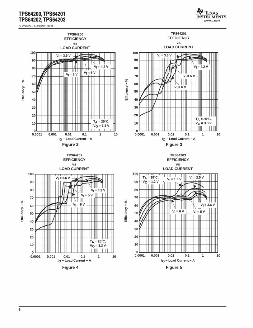
TYPICAL CHARACTERISTICS
All graphs were generated using the circuit as shown unless otherwise noted. For output voltages other than3.3 V, the output voltage divider was changed accordingly. Graphs for the TPS64203 were taken using theapplication circuit shown in Figure 25.
SW
CDRH103R−100
Si5447DC
MBRM120LT3
EN
GND
FB
VIN
ISENSE
VI
CI10 µF
X7R
TPS6420x
R(ISENSE) = 33 mΩ
R1620 kΩ
R2360 kΩ
Cff4.7 pF
Co47 µF PosCap6TPA47M
VO
1
2
3
6
5
4
10 µH
Figure 1. Basic Application Circuit For a 2-A Step-Down Converter
TABLE OF GRAPHS
FIGURE
η Efficiency vs Load current 2 − 5
Output voltage vs Output current 6 − 9
Switching frequency vs Output current 10 − 13
Operating quiescent current vs Input voltage 14
Output voltage ripple 15
Line transient response Using circuit according to Figure 1 16
Load transient response Using circuit according to Figure 1 17
Start-up timing Using circuit according to Figure 1 18
SLVS485 − AUGUST 2003
www.ti.com
6
Figure 2
0
10
20
30
40
50
60
70
80
90
100
0.0001 0.001 0.01 0.1 1 10
VI = 3.6 V
VI = 4.2 V
VI = 5 VVI = 6 V
TA = 25°C,VO = 3.3 V
TPS64200EFFICIENCY
vsLOAD CURRENT
IO − Load Current − A
Effi
cien
cy −
%
Figure 3
0
10
20
30
40
50
60
70
80
90
100
VI = 4.2 V
VI = 6 V
TA = 25°C,VO = 3.3 V
TPS64201EFFICIENCY
vsLOAD CURRENT
IO − Load Current − A
Effi
cien
cy −
%
VI = 3.6 V
VI = 5 V
0.0001 0.001 0.01 0.1 1 10
Figure 4
0
10
20
30
40
50
60
70
80
90
100
VI = 4.2 V
VI = 6 V
TA = 25°C,VO = 3.3 V
TPS64202EFFICIENCY
vsLOAD CURRENT
IO − Load Current − A
Effi
cien
cy −
%
VI = 3.6 V
VI = 5 V
0.0001 0.001 0.01 0.1 1 100
10
20
30
40
50
60
70
80
90
100
VI = 6 V
TA = 25°C,VO = 1.2 V
TPS64203EFFICIENCY
vsLOAD CURRENT
IO − Load Current − A
Effi
cien
cy −
%
VI = 1.8 V VI = 2.5 V
VI = 3.6 V
VI = 5 V
0.0001 0.001 0.01 0.1 1 10
Figure 5
SLVS485 − AUGUST 2003
www.ti.com
7
3.20
3.22
3.24
3.26
3.28
3.30
3.32
3.34
3.36
3.38
3.40
VI = 3.6 V
VI = 4.2 VVI = 6 V
TA = 25°C,VO = 3.3 V
VI = 5 V
TPS64200OUTPUT VOLTAGE
vsOUTPUT CURRENT
− O
utpu
t Vol
tage
− V
VO
IO − Output Current − A0.0001 0.001 0.01 0.1 1 10
Figure 6 Figure 7
3.20
3.22
3.24
3.26
3.28
3.30
3.32
3.34
3.36
3.38
3.40
VI = 3.6 V
VI = 4.2 V
TA = 25°C,VO = 3.3 V
VI = 5 V
TPS64201OUTPUT VOLTAGE
vsOUTPUT CURRENT
− O
utpu
t Vol
tage
− V
VO
IO − Output Current − A
VI = 6 V
0.0001 0.001 0.01 0.1 1 10
Figure 8
3.20
3.22
3.24
3.26
3.28
3.30
3.32
3.34
3.36
3.38
3.40
VI = 3.6 V
TA = 25°C,VO = 3.3 V VI = 5 V
TPS64202OUTPUT VOLTAGE
vsOUTPUT CURRENT
− O
utpu
t Vol
tage
− V
VO
IO − Output Current − A
VI = 6 V
VI = 4.2 V
0.0001 0.001 0.01 0.1 1 10
Figure 9
1.15
1.17
1.19
1.21
1.23
1.25
1.27
1.29 TA = 25°C,VO = 1.2 V
TPS64203OUTPUT VOLTAGE
vsOUTPUT CURRENT
− O
utpu
t Vol
tage
− V
VO
IO − Output Current − A
VI = 6 VVI = 5 VVI = 3.6 V
VI = 2.5 VVI = 1.8 V
0.0001 0.001 0.01 0.1 1 10
SLVS485 − AUGUST 2003
www.ti.com
8
Figure 10
0
50
100
150
200
250
300
350
400
0.001 0.01 0.1 1 10
f − F
requ
ency
− k
Hz
TPS64200SWITCHING FREQUENCY
vsOUTPUT CURRENT
IO − Output Current − A
VO = 3.3 V
VO = 1.2 V
VI = 5 V
Figure 11
0
50
100
150
200
250
300
350
400
450
500
0.001 0.01 0.1 1 10f −
Fre
quen
cy −
kH
z
TPS64201SWITCHING FREQUENCY
vsOUTPUT CURRENT
IO − Output Current − A
VO = 3.3 V
VO = 1.2 V
VI = 5 V
Figure 12
0
50
100
150
200
250
300
350
400
450
500
550
600
0.001 0.01 0.1 1 10
f − F
requ
ency
− k
Hz
TPS64202SWITCHING FREQUENCY
vsOUTPUT CURRENT
IO − Output Current − A
VI = 4.2 VVI = 3.8 V
VI = 3.8 V,Cff = 165 pF
VO = 3.3 V0
100
200
300
400
500
600
700
800
900
0.001 0.01 0.1 1 10
f − F
requ
ency
− k
Hz
TPS64203SWITCHING FREQUENCY
vsOUTPUT CURRENT
IO − Output Current − A
VO = 1.2 V
VO = 3.3 V,Cff = 165 pF
VI = 5 V
Figure 13
SLVS485 − AUGUST 2003
www.ti.com
9
Figure 14
0
5
10
15
20
25
30
35
40
0 0.5 1 1.5 2 2.5 3 3.5 4 4.5 5 5.5 6 6.5
− O
pera
ting
Qui
esce
nt C
urre
nt −
AµQI
TPS642000OPERATING QUIESCENT CURRENT
vsINPUT VOLTAGE
VI − Input Voltage − V
TA = 85°CTA = 25°C
TA = −40°C
TPS64200OUTPUT VOLTAGE RIPPLE
VI = 3.8 V,VO = 1.2 V,RL = 1.2 Ω,TA = 25°C
VO
I(coil)
IO = 1000 mA
Figure 15
200
mA
/Div
2 s/Div20
mV
/Div
Figure 16
VO
VI
VI = 3.8 V to 5 V,VO = 1.2 V,RL = 1.2 Ω,TA = 25°C
TPS64200LINE TRANSIENT RESPONSE
20 m
V/D
iv
40 s/Div
1 V
/Div
Figure 17
VO
IO
VI = 5 V,VO = 3.3 V,IL = 200 mA to 1800 mA,TA = 25°C
TPS64203LOAD TRANSIENT RESPONSE
50 m
V/D
iv
50 s/Div
1 A
/Div
SLVS485 − AUGUST 2003
www.ti.com
10
Figure 18
TPS64200STARTUP TIMING
EN
VO
II
I(Inductor)
VI = 3.8 V,VO = 3.3 V,RL = 1.66 Ω,TA = 25°C
100 s/Div
DETAILED DESCRIPTION
Operation
The TPS6420x is a nonsynchronous step-down controller which is operating with a minimum on-time/minimumoff-time control. An external PMOS is turned on until the output voltage reaches its nominal value or the currentlimit is exceeded. If the current limit is exceeded, the PMOS is switched off and stays off for the minimumoff-time. After that the PMOS is switched on again. When the nominal output voltage is reached, the PMOSis switched off and stays off until the output voltage dropped below its nominal value.
Operating Modes
When delivering low or medium output current, the TPS6420x operate in discontinuous mode. With everyswitching cycle, the current in the inductor starts at zero, rises to a maximum value and ramps down to zeroagain. As soon as the current in the inductor drops to zero, ringing occurs at the resonant frequency of theinductor and stray capacitance, due to residual energy in the inductor when the diode turns off. Ringing indiscontinuous mode is normal and does not have any influence on efficiency. The ringing does not contain muchenergy and can easily be damped by an RC snubber. See the application section for further details.
With high output current, the TPS6420x operate in continuous current mode. In this mode, the inductor currentdoes not drop to zero within one switching cycle. The output voltage in continuous mode is directly dependanton the duty cycle of the switch.
Variable Minimum On-Time (TPS64201 to TPS64202 Only)
The minimum on-time of the device is 1.6 µs. At light loads, this would cause a low switching frequency in theaudible range because the energy transferred to the output during the on-time would cause a higher rise in theoutput voltage than needed and therefore lead to a long off−time until the output voltage dropped again. To avoida switching frequency in the audible range the TPS64201 and TPS64202 can internally reduce the minimumon time in three steps from 1.6 µs to 800 ns, 400 ns and 200 ns. The on-time is reduced by one step if theswitching frequency dropped to a lower value than 50 kHz. This keeps the frequency above the audio frequencyover a wide load range and also keeps the output voltage ripple low.
SLVS485 − AUGUST 2003
www.ti.com
11
Soft Start
The TPS6420x has an internal soft start circuit that limits the inrush current during start up. This preventspossible voltage drops of the input voltage in case a battery or a high impedance power source is connectedto the input of the TPS6420x. During soft start the current limit is increased from 25% of its maximum to themaximum within about 250 µs.
100% Duty Cycle Low Dropout Operation
The TPS6420x offers the lowest possible input to output voltage difference while still maintaining regulation withthe use of the 100% duty cycle mode. In this mode the P-channel switch is constantly turned on. This isparticularly useful in battery powered applications to achieve longest operation time by taking full advantageof the whole battery voltage range.
Enable
A voltage higher than the EN trip point of 1.3 V up to the input voltage forces the TPS64200 into shutdown. Inshutdown, the power switch, drivers, voltage reference, oscillator, and all other functions are turned off. Thesupply current is reduced to less than 1 µA in shutdown. Pulling enable low starts up the TPS64200 with thesoftstart as described under the chapter softstart.
Undervoltage Lockout
The undervoltage lockout circuit prevents the device from misoperation at low input voltages. Basically, itprevents the converter from turning on the external PMOS under undefined conditions.
Current Limit
The ISENSE input is used to set the current limit for the external PMOS. The sense resistor must be connectedbetween VI and source of the external PMOS. The ISENSE pin is connected to the source of the externalPMOS. The maximum current is calculated by:
I(cur lim) V(ISENSE)
RS
(1)
For low cost solutions the rDS(on) of the external PMOS can also be used to set the current limit. In this casethe ISENSE pin is connected to the drain of the PMOS. The current in the PMOS is automatically sampled bythe TPS6420x some 10 ns after the PMOS is turned on. The ISENSE pin should always be connected to eitherthe source of the PMOS or the drain if an additional sense resistor is used. Otherwise there is no workingovercurrent protection and no soft start in the system. The maximum drain current if the rDS(on) is used as asense resistor is calculated by:
I(cur lim) V(ISENSE)
rDS(on)(2)
Short-Circuit Protection
With a controller only limited short circuit protection is possible because the temperature of the externalcomponents is not supervised. In an overload condition, the current in the external diode may exceed themaximum rating. To protect the diode against overcurrent, the off-time of the TPS6420x is increased when thevoltage at the feedback pin is lower than its nominal value. The off-time when the output is shorted (feedbackvoltage is zero) is about 4 µs. This allows the current in the external diode to drop until the PMOS is turned onagain and the overcurrent protection switches off the PMOS again. The off-time is directly proportional to thevoltage at feedback.
SLVS485 − AUGUST 2003
www.ti.com
12
THEORY OF OPERATIONThe basic application circuit for the TPS64200 is shown in Figure 1. External component selection is driven bythe load requirement. It begins with the selection of the current sense resistor R(ISENSE) followed by the outputdiode, the inductor L, and the output and input capacitors. The inductor is chosen based on the desired amountof ripple current and switching frequency. The output capacitor is chosen large enough to meet the requiredoutput ripple and transient requirements. The ESR of the output capacitor is needed for stability of the converter.Therefore, an output capacitor with a certain amount of ESR is needed for the standard application circuit. Seethe application information for more details. The input capacitor must be capable of handling the required RMSinput current.
Setting the Inductor Current LimitThe ISENSE pin is connected to an internal current comparator with a threshold of 120 mV/R(ISENSE). The currentcomparator sets the peak inductor current. As the current limit is intended to protect the external PMOS thelimit must not be reached in normal operation. Set the current limit to about 1.3 times the maximum outputcurrent or higher if desired. This takes into account a certain amount of inductor current ripple. The current limitmay also influence the start-up time when the current limit is exceeded during start up.
R(ISENSE) V(ISENSE) min
1.3 IO
IO — maximum output current in continuous conduction modeV(ISENSE), min = 90 mV
(3)
The current sense resistor’s power rating should be:
P(ISENSE)
V(ISENSE) max2
R(ISENSE)
V(ISENSE), max = 120 mV (4)
Setting the Output VoltageThe output voltage of the TPS64200 to TPS64202 can be set using an external resistor divider. The sum ofR1 and R2 should not exceed 1 MΩ to keep the influence of leakage current into the feedback pin low.
VO VFB
R1 R2R2
R1 R2
VOVFB R2 with VFB = 1.2 V (5)
In some applications, depending on the layout, the capacitance may be too high from FB to GND. In this case,the internal comparator may not switch fast enough to operate with the minimum on-time or the minimumoff-time given in this data sheet. For such applications a feedforward capacitor (Cff) in the range of 4.7 pF to47 pF (typical) is added in parallel with R1 to speed up the comparator. Choose a capacitor value that is highenough that the device turns on the PMOS for its minimum on-time with no load at the output.
Selecting the Input CapacitorThe input capacitor is used to reduce peak currents drawn from the power source and reduces noise and voltageripple on the input of the converter, caused by its switching action. Use low ESR tantalum capacitors orpreferably X5R or X7R ceramic capacitors with a voltage rating higher than the maximum supply voltage in theapplication. In continuous conduction mode, the input capacitor must handle an rms-current which is given by:
ICin(rms) IO
VOVI, min
(6)
Select the input capacitor according to the calculated rms-input current requirements and according to themaximum voltage ripple. Use a minimum value of 10 µF:
CI, min
12 L
IL
2
V(ripple) VI
12 L
0.3 IO
2
V(ripple) VI
with: V(ripple) − voltage ripple at CI ∆IL − inductor current ripple (7)
SLVS485 − AUGUST 2003
www.ti.com
13
For a first approximation use:
L = 10 µH
V(ripple) = 150 mV (verify in the application)
Selecting the Inductor Value
The main parameters when choosing the inductor are current rating and inductance. The inductance mainlydetermines the inductor current ripple. The TPS6420x operates with a wide range of inductor values. Valuesbetween 4.7 µH and 47 µH work in most applications. Select an inductor with a current rating exceeding thelimit set by R(ISENSE) or rDS(on). The first step in inductor design is to determine the operating mode of theTPS64200. The device can either work with minimum-on-time or minimum-off-time, depending on input voltageand output voltage.
The device works with minimum-on-time if:
VI VO IO rDS(on) RRL x IO
toff, min VO VSCHOTTKY RRL IO
ton, min
with RRL − inductor resistance
(8)
with L
V tI
For minimum-on-time:
L
VI–VO–IO rDS(on)–RRL IO ton, min
Iwith: ∆I ≤ 0.3 × IO (9)
For minimum-off-time:
L
VO VSCHOTTKY RRL IO toff, min
I(10)
Table 1. List of Inductors Tested With the TPS6420x
MANUFACTURER TYPE INDUCTANCE DC RESISTANCE SATURATION CURRENT
TDK SLF7032T−100M1R4 10 µH ±20% 53 mΩ ±20% 1.4 A
TDK SLF6025−150MR88 15 µH ±20% 85 mΩ ±20% 0.88 A
Sumida CDRH6D28−5R0 5 µH 23 mΩ 2.4 A
Sumida CDRH103R−100 10 µH 45 mΩ 2.4 A
Sumida CDRH4D28−100 10 µH 95 mΩ 1.0 A
Sumida CDRH5D18−6R2 6.2 µH 71 mΩ 1.4 A
Coilcraft DO3316P−472 4.7 µH 18 mΩ 5.4 A
Coilcraft DT3316P−153 15 µH 60 mΩ 1.8 A
Coilcraft DT3316P−223 22 µH 84 mΩ 1.5 A
Wurth 744 052 006 6.2 µH 80 mΩ 1.45 A
Wurth 74451115 15 µH 90 mΩ 0.8 A
SLVS485 − AUGUST 2003
www.ti.com
14
Selecting the External PMOS
An external PMOS must be used for a step-down converter with the TPS64200. The selection criteria for thePMOS are threshold voltage, rDS(on), gate charge and current and voltage rating. Since the TPS64200 canoperate down to 1.8 V, the external PMOS must have a VGS(th) much lower than that if it is operated with sucha low voltage. As the gate of the PMOS finds the full supply voltage applied to the TPS64200, the PMOS mustbe able to handle that voltage at the gate. The drain to source breakdown voltage rating should be at least afew volts higher than the supply voltage in the application. The rms-current in the PMOS assuming low inductorcurrent ripple and continuous conduction mode, is:
IPMOS(rms) IO D IO
VOVI
(11)
The power dissipated in the PMOS is comprised of conduction losses and switching losses. The conductionlosses are a function of the rms−current in the PMOS and the rDS(on) at a given temperature. They are calculatedusing:
P(cond) IO D
2 rDS(on) 1 TC TJ–25°C IO D
2 rDS(on)
with TC = 0.005/°C(12)
Table 2. PMOS Transistors Used in the Application Section
TYPE MANUFACTURER rDS(on) VDS ID PACKAGE
Si5447DC Vishay Siliconix 0.11 Ω at VGS = −2.5 V −20 V −3.5 A at 25°C 1206
Si5475DC Vishay Siliconix 0.041 Ω at VGS = −2.5 V −12 V −6.6 A at 25°C 1206
Si2301ADS Vishay Siliconix 0.19 Ω at VGS = −2.5 V −20 V −1.4 A at 25°C SOT23
Si2323DS Vishay Siliconix 0.41 Ω at VGS = −2.5 V −20 V −4.1 A at 25°C SOT23
FDG326P Fairchild 0.17 Ω at VGS = −2.5 V −20 V −1.5 A SC70
Selecting the Output Diode
The output diode conducts in the off phase of the PMOS and carries the full output current. The high switchingfrequency demands a high-speed rectifier. Schottky diodes are recommended for best performance. Make surethat the peak current rating of the diode exceeds the peak current limit set by the sense resistor R(ISENSE) orrDS(on). Select a Schottky diode with a low reverse leakage current to avoid an increased supply current. Theaverage current in the diode in continuous conduction mode, assuming low inductor current ripple, is:
I(diode)(Avg) IO(1–D) IO1–VOVI (13)
Table 3. Tested Diodes
TYPE MANUFACTURER VR IF PACKAGE
MBRM120LT3 On Semiconductor 20 V 1 A DO216AA
MBR0530T1 On Semiconductor 30 V 0.5 A SOD123
ZHCS2000TA Zetex 40 V 2 A SOT23−6
B320 Diodes Inc. 20 V 3 A SMA
SLVS485 − AUGUST 2003
www.ti.com
15
Selecting the Output CapacitorThe value of the output capacitor depends on the output voltage ripple requirements as well as the maximumvoltage deviation during a load transient. The TPS6420x require a certain ESR value for proper operation. LowESR tantalum capacitors or PosCap work best in the application. A ceramic capacitor with up 1 µF may be usedin parallel for filtering short spikes. The output voltage ripple is a function of both the output capacitance andthe ESR value of the capacitor. For a switching frequency which is used with the TPS6420x, the voltage rippleis typically between 90% and 95% due to the ESR value.
Vpp I ESR 1
8 CO ƒ 1.1 I ESR (14)
ESR, max
Vpp1.1 I
(15)
The output capacitance typically increases with load transient requirements. For a load step from zero outputcurrent to its maximum, the following equation can be used to calculate the output capacitance:
CO
L I 2O
(VI VO) x V (16)
Table 4. Capacitors Used in the Application
TYPE MANUFACTURER CAPACITANCE ESR VOLTAGE RATING
6TPB47M (PosCap) Sanyo 47 µF 0.1 Ω 6.3 V
T491D476M010AS Kemet 47 µF 0.8 Ω 10 V
B45197A Epcos 47 µF 0.175 Ω 16 V
B45294−R1107−M40 Epcos 100 µF 0.045 Ω 6.3 V
594D476X0016C2 Vishay 47 µF 0.11 Ω 16 V
Output Voltage RippleOutput voltage ripple causes the output voltage to be higher or lower than set by the resistor divider at thefeedback pin. If the application runs with minimum on-time, the ripple (half of the peak-to-peak value) adds tothe output voltage. In an application which runs with minimum off-time, the output voltage is lower by the amountof ripple (half of the peak-to-peak value) at the output.
Snubber DesignFor low output current, the TPS6420x work in discontinuous current mode. When the current in the inductordrops to zero, the inductor and parasitic capacitance form a resonant circuit, which causes oscillations whenboth, diode and PMOS do not conduct at the end of each switching cycle. The oscillation can easily be dampedby a RC-snubber. The first step in the snubber design is to measure the oscillation frequency of the sine wave.Then, a capacitor has to be connected in parallel to the Schottky diode which causes the frequency to drop tohalf of its original value. The resistor is selected for optimum transient response (aperiodic).
R 2fL f − measured resonant frequencyL − inductance used
(17)
Selecting the Right Device for the ApplicationThe TPS6420x step-down controllers either operate with a fixed on-time or a fixed off-time control. It mainlydepends on the input voltage to output voltage ratio if the switching frequency is determined by theminimum-on-time or the minimum-off-time. To select the right device for an application see the table below:
INPUT TO OUTPUT VOLTAGE RATIOSWITCHING FREQUENCY
DETERMINED BY
PROPOSED DEVICE FORHIGH SWITCHING
FREQUENCY
PROPOSED DEVICE FORLOW SWITCHING
FREQUENCY
VI >> VO (e.g. VI = 5 V VO = 1.5 V) Minimum on−time TPS64203 TPS64200, TPS64201
VI ≈ VO (e.g. VI = 3.8 V VO = 3.3 V) Minimum off−time TPS64202 TPS64200, TPS64201
SLVS485 − AUGUST 2003
www.ti.com
16
APPLICATION INFORMATION
SW
CDRH6D28-5R0
Si5475DC
MBRM120LT3
EN
GND
FB
VIN
ISENSE
Li-lon3.3 V to 4.2 V
CIN10 µF TPS64202
R(ISENSE) = 33 mΩ
R1620 kΩ
R2360 kΩ
Cff4.7 pF
Co47 F PosCap6TPA47M
3.3 V / 2 A
1
2
3
6
5
4
5 µH
Figure 19. Application For a Li-Ion to 3.3-V / 2-A Conversion
The TPS64202 was used for this application because for a low input to output voltage difference, the switchingfrequency is determined by the minimum off-time. The TPS64202 with its minimum off-time of 300 ns providesa higher switching frequency compared to the other members of the TPS6420x family.
SW
CDRH6D28-5R0
Si5475DC
MBRM120LT3
EN
GND
FB
VIN
ISENSE
Li-lon3.3 V to 4.2 V
CIN10 µF TPS64202
R1620 kΩ
R2360 kΩ
Cff4.7 pF
Co47 F PosCap6TPA47M
3.3 V / 2 A
R3150 Ω
C3470 pF
1
2
3
6
5
4
5 µH
Figure 20. Application For a Li-Ion to 3.3-V / 2-A Conversion Using r DS(on) Sense and RC SnubberNetwork For the Schottky Diode
SLVS485 − AUGUST 2003
www.ti.com
17
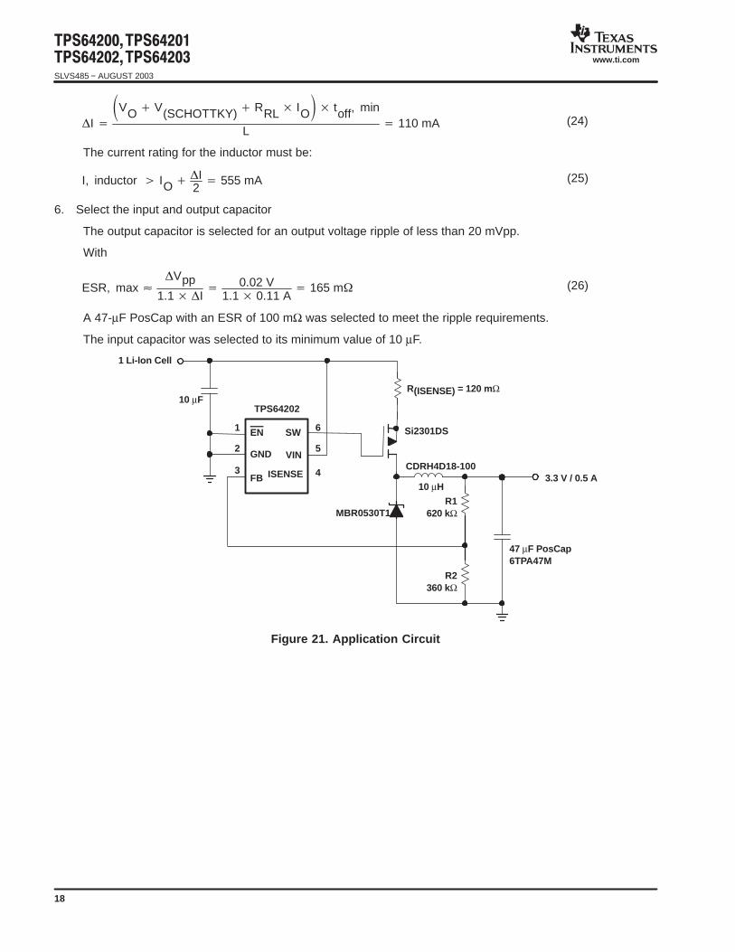
DESIGN EXAMPLE FOR AN APPLICATION USING A LI-ION CELL (3.3 V TO 4.2 V) TOGENERATE 3.3 V/500 mA
1. Calculate the sense resistor for the current limit:
R(ISENSE) V(ISENSE) min
1.3 IO
90 mV1.3 0.5 A
138 m (18)
Choose the next lower standard value : R(ISENSE) = 120 mΩ. Verify the inductor current ripple after the inductorhas been determined in step 5.
If the rDS(on) of the PMOS is used to sense the inductor current, a PMOS with less than 138 mΩ must be usedfor the application.
2. Calculate the resistors for the output voltage divider using VO = 3.3 V and VFB = 1.21 V
R1 R2
VOVFB–R2 1.72 R2 (19)
Choose R2 = 360 kΩ, and then get R1 = 619 kΩ. Select the next standard value: R1 = 620 kΩ
3. Select the external PMOS
For a Li-Ion to 3.3-V conversion, the minimum input voltage is 3.3 V. Therefore, the converter runs in 100%mode (duty cycle=1) and the maximum PMOS current is equal to the output current.
I(PMOS) IO 0.5 A (20)
The Si2301ADS is selected for this application because it meets the requirements when an external senseresistor is used. Otherwise a PMOS with less rDS(on) must be selected.
Verify the maximum power dissipation of the PMOS using:
P(cond) IO
2 rDS(on) (0.5 A)2
0.19 48 mW (21)
4. Select the external diode
For the Schottky diode, the worst case current is at high input voltage (4.2 V for a Li-Ion cell).
I(diode)(Avg) IO1–VOVI IO
1– 3.3 V4.2 V
0.11 A (22)
The MBR0530T1 is selected because it meets the voltage and current requirements. The forward voltage isabout 0.3 V. Do not use a Schottky diode which is much larger than required as it also typically has more leakagecurrent and capacitance which reduces efficiency.
5. Calculate the inductor value.
If the output voltage is close to the input voltage, the switching frequency is determined by the minimum off-time.Therefore, the TPS64202 is used for the maximum switching frequency possible. Allow an inductor ripplecurrent of 0.3 × IO for the application. For the inductor, a series resistance of 100 mΩ is assumed.
For minimum-off-time, the inductor value is:
L
VO V(SCHOTTKY) RRL IO toff, min
I
(3.3 V 0.3 V 0.05 V) 0.3 s0.3 0.5 A
7.3 H
(23)
For a low inductor current ripple, select the next available larger inductor with L = 10 µH. This provides aninductor ripple current of 110 mA (peak-to-peak).
SLVS485 − AUGUST 2003
www.ti.com
18
I VO V(SCHOTTKY) RRL IO
toff, min
L 110 mA (24)
The current rating for the inductor must be:
(25)I, inductor IO
I2
555 mA
6. Select the input and output capacitor
The output capacitor is selected for an output voltage ripple of less than 20 mVpp.
With
ESR, max
Vpp1.1 I
0.02 V1.1 0.11 A
165 m (26)
A 47-µF PosCap with an ESR of 100 mΩ was selected to meet the ripple requirements.
The input capacitor was selected to its minimum value of 10 µF.
SW
CDRH4D18-100
Si2301DS
MBR0530T1
EN
GND
FB
VIN
ISENSE
1 Li-lon Cell
10 µFTPS64202
R1620 kΩ
R2360 kΩ
47 µF PosCap6TPA47M
3.3 V / 0.5 A
R(ISENSE) = 120 mΩ
1
2
3
6
5
410 µH
Figure 21. Application Circuit
SLVS485 − AUGUST 2003
www.ti.com
19
SW
CDRH103R-100
Si5447DC
ZHCS200
EN
GND
FB
VIN
ISENSE
5 V
10 µFTPS64200
R1620 kΩ
R2360 kΩ
47 F PosCap6TPA47M
3.3 V / 2 A
R(ISENSE) = 33 mΩ
1
2
3
6
5
4
10 µH
Figure 22. Application For a 5-V to 3.3-V / 2-A Conversion
Inverter Using TPS64200
SW
MBR0530T1
Si2301DSEN
GND
FB
VIN
ISENSE
VI2.7 V to 4.2 V
10 µFTPS64200
R(ISENSE) = 33 mΩ
47 µFX7R
−5 V / 0.1 A
CDRH4D28-100
100 kΩ
R1
_
+
VI24 kΩ
R2
SW
OPA363
1
2
3
6
5
4
10 µH
Figure 23. Application For an Inverter Using TPS64200
SLVS485 − AUGUST 2003
www.ti.com
20
The TPS6420x can be used for an inverter. Only one additional operational amplifier is required for thisapplication. When the PMOS is switched on, the current in the inductor ramps up to its maximum, set by Rs.Then the PMOS is switched off, the energy stored in the inductor is transferred to the output. The output voltageand the maximum output current can be calculated using:
VO
R1R2
VFB IO max 0.8
VI–VO
V(ISENSE)2R(ISENSE)
(27)
OLED Power Supply
The TPS6420x can be combined with a TPS61045 boost converter for a OLED power supply.
SW
MBR0530T1
Si2301DSEN
GND
FB
VIN
ISENSE
VI1.8 V to 5.5 V
10 µFTPS64200
R(ISENSE) = 150 mΩ
47 µFX7R
−7 V / 50 mA
CDRH4D28-100
750 kΩ
R1
_
+
VI130 kΩ
R2
SW
OPA363
SWL
VIN
GND
DO
FBCTRL
PGND
4.7 µH
56 kΩ
12 kΩ
22 pF4.7 µF
TPS61045
7 V / 50 mA1 µFX7R
1
2
3
6
5
4
1
2
5
8
3
4
6 7
10 µH
Figure 24. Application For a OLED Power Supply
SLVS485 − AUGUST 2003
www.ti.com
21
SW
Wurth 744052006
Si2323DS
MBRM120LT3
EN
GND
FB
VIN
ISENSE
5 V
10 µFX5R TPS64203
100 µF/6.3 VB45294-R1107-M40
1.2 V / 1.2 A
1
2
3
6
5
4
6.2 µH
Figure 25. Application For a 5-V to 1.2-V / 1.2-A Conversion
SW
DO3316P−472
Si5475DC
B320
EN
GND
FB
VIN
ISENSE
5 V
CIN22 µF TPS64202
R1620 kΩ
R2360 kΩ
Cff4.7 pF
Co100 F PosCap6TPC100M
3.3 V / 3 A
1
2
3
6
5
4
4.7 µH
R(ISENSE) = 20 mΩ
Figure 26. Application For a 5-V to 3.3-V / 3-A Conversion
SLVS485 − AUGUST 2003
www.ti.com
22
Ceramic Output Capacitor
SW
CDRH6D28-100
Si5475DC
MBRM120LT3
EN
GND
FB
VIN
ISENSE
5 V
CI10 µF TPS64203
R1a680 kΩ
R2300 kΩ
Cff82 pF
Co22 µF X5R6.3 V
3.3 V / 2 A
R1b2.2 MΩ
R(ISENSE) = 33 mΩ
R(GATE)
10 Ω
1
2
3
6
5
4
10 µH
Figure 27. Application Using a Ceramic Output Capacitor
The control scheme of the TPS6420x usually requires an output capacitor with some tens of milliohms of ESRfor stability, which is usually the case for tantalum capacitors. This application circuit above also works withceramic capacitors. Resistor R1b is used to add an additional control signal to the feedback loop, which iscoupled into the FB pin. The circuit works best with R1b = 2 …4 x R1a. If the resistance of R1b is too lowcompared to R1a, the more load regulation the output voltage shows, but stability is best. The advantage ofthis circuit is a very low output voltage ripple and small size. The gate resistor shown can be used in everyapplication. It minimizes switching noise of the converter and, therefore, increases stability and provides loweroutput voltage ripple. However, it decreases efficiency slightly because the rise and fall time, and the associatedlosses are larger.
(28)R1
11
R1a
1R1b
R1b
11
R1– 1
R1a
Use the following equation to calculate R1a if R1b = 4R1a
R1a
54
R1 (29)
PACKAGE OPTION ADDENDUM
www.ti.com 11-Apr-2013
Addendum-Page 1
PACKAGING INFORMATION
Orderable Device Status(1)
Package Type PackageDrawing
Pins PackageQty
Eco Plan(2)
Lead/Ball Finish MSL Peak Temp(3)
Op Temp (°C) Top-Side Markings(4)
Samples
TPS64200DBVR ACTIVE SOT-23 DBV 6 3000 Green (RoHS& no Sb/Br)
CU NIPDAU Level-1-260C-UNLIM -40 to 85 PJAI
TPS64200DBVRG4 ACTIVE SOT-23 DBV 6 3000 Green (RoHS& no Sb/Br)
CU NIPDAU Level-1-260C-UNLIM -40 to 85 PJAI
TPS64200DBVT ACTIVE SOT-23 DBV 6 250 Green (RoHS& no Sb/Br)
CU NIPDAU Level-1-260C-UNLIM -40 to 85 PJAI
TPS64200DBVTG4 ACTIVE SOT-23 DBV 6 250 Green (RoHS& no Sb/Br)
CU NIPDAU Level-1-260C-UNLIM -40 to 85 PJAI
TPS64201DBVR ACTIVE SOT-23 DBV 6 3000 Green (RoHS& no Sb/Br)
CU NIPDAU Level-1-260C-UNLIM -40 to 85 PJBI
TPS64201DBVRG4 ACTIVE SOT-23 DBV 6 3000 Green (RoHS& no Sb/Br)
CU NIPDAU Level-1-260C-UNLIM -40 to 85 PJBI
TPS64201DBVT ACTIVE SOT-23 DBV 6 250 Green (RoHS& no Sb/Br)
CU NIPDAU Level-1-260C-UNLIM -40 to 85 PJBI
TPS64201DBVTG4 ACTIVE SOT-23 DBV 6 250 Green (RoHS& no Sb/Br)
CU NIPDAU Level-1-260C-UNLIM -40 to 85 PJBI
TPS64202DBVR ACTIVE SOT-23 DBV 6 3000 Green (RoHS& no Sb/Br)
CU NIPDAU Level-1-260C-UNLIM -40 to 85 PJCI
TPS64202DBVRG4 ACTIVE SOT-23 DBV 6 3000 Green (RoHS& no Sb/Br)
CU NIPDAU Level-1-260C-UNLIM -40 to 85 PJCI
TPS64202DBVT ACTIVE SOT-23 DBV 6 250 Green (RoHS& no Sb/Br)
CU NIPDAU Level-1-260C-UNLIM -40 to 85 PJCI
TPS64202DBVTG4 ACTIVE SOT-23 DBV 6 250 Green (RoHS& no Sb/Br)
CU NIPDAU Level-1-260C-UNLIM -40 to 85 PJCI
TPS64203DBVR ACTIVE SOT-23 DBV 6 3000 Green (RoHS& no Sb/Br)
CU NIPDAU Level-1-260C-UNLIM -40 to 85 PJDI
TPS64203DBVRG4 ACTIVE SOT-23 DBV 6 3000 Green (RoHS& no Sb/Br)
CU NIPDAU Level-1-260C-UNLIM -40 to 85 PJDI
TPS64203DBVT ACTIVE SOT-23 DBV 6 250 Green (RoHS& no Sb/Br)
CU NIPDAU Level-1-260C-UNLIM -40 to 85 PJDI
TPS64203DBVTG4 ACTIVE SOT-23 DBV 6 250 Green (RoHS& no Sb/Br)
CU NIPDAU Level-1-260C-UNLIM -40 to 85 PJDI
(1) The marketing status values are defined as follows:ACTIVE: Product device recommended for new designs.
LIFEBUY: TI has announced that the device will be discontinued, and a lifetime-buy period is in effect.NRND: Not recommended for new designs. Device is in production to support existing customers, but TI does not recommend using this part in a new design.PREVIEW: Device has been announced but is not in production. Samples may or may not be available.OBSOLETE: TI has discontinued the production of the device.
(2) Eco Plan - The planned eco-friendly classification: Pb-Free (RoHS), Pb-Free (RoHS Exempt), or Green (RoHS & no Sb/Br) - please check http://www.ti.com/productcontent for the latest availabilityinformation and additional product content details.TBD: The Pb-Free/Green conversion plan has not been defined.Pb-Free (RoHS): TI's terms "Lead-Free" or "Pb-Free" mean semiconductor products that are compatible with the current RoHS requirements for all 6 substances, including the requirement thatlead not exceed 0.1% by weight in homogeneous materials. Where designed to be soldered at high temperatures, TI Pb-Free products are suitable for use in specified lead-free processes.Pb-Free (RoHS Exempt): This component has a RoHS exemption for either 1) lead-based flip-chip solder bumps used between the die and package, or 2) lead-based die adhesive used betweenthe die and leadframe. The component is otherwise considered Pb-Free (RoHS compatible) as defined above.Green (RoHS & no Sb/Br): TI defines "Green" to mean Pb-Free (RoHS compatible), and free of Bromine (Br) and Antimony (Sb) based flame retardants (Br or Sb do not exceed 0.1% by weightin homogeneous material)
(3) MSL, Peak Temp. -- The Moisture Sensitivity Level rating according to the JEDEC industry standard classifications, and peak solder temperature.
(4) Multiple Top-Side Markings will be inside parentheses. Only one Top-Side Marking contained in parentheses and separated by a "~" will appear on a device. If a line is indented then it is acontinuation of the previous line and the two combined represent the entire Top-Side Marking for that device.
Important Information and Disclaimer:The information provided on this page represents TI's knowledge and belief as of the date that it is provided. TI bases its knowledge and belief on informationprovided by third parties, and makes no representation or warranty as to the accuracy of such information. Efforts are underway to better integrate information from third parties. TI has taken andcontinues to take reasonable steps to provide representative and accurate information but may not have conducted destructive testing or chemical analysis on incoming materials and chemicals.TI and TI suppliers consider certain information to be proprietary, and thus CAS numbers and other limited information may not be available for release.
In no event shall TI's liability arising out of such information exceed the total purchase price of the TI part(s) at issue in this document sold by TI to Customer on an annual basis.
Texas Instruments Incorporated (TI) reserves the right to make corrections, enhancements, improvements and other changes to itssemiconductor products and services per JESD46, latest issue, and to discontinue any product or service per JESD48, latest issue. Buyersshould obtain the latest relevant information before placing orders and should verify that such information is current and complete.TI’s published terms of sale for semiconductor products (http://www.ti.com/sc/docs/stdterms.htm) apply to the sale of packaged integratedcircuit products that TI has qualified and released to market. Additional terms may apply to the use or sale of other types of TI products andservices.Reproduction of significant portions of TI information in TI data sheets is permissible only if reproduction is without alteration and isaccompanied by all associated warranties, conditions, limitations, and notices. TI is not responsible or liable for such reproduceddocumentation. Information of third parties may be subject to additional restrictions. Resale of TI products or services with statementsdifferent from or beyond the parameters stated by TI for that product or service voids all express and any implied warranties for theassociated TI product or service and is an unfair and deceptive business practice. TI is not responsible or liable for any such statements.Buyers and others who are developing systems that incorporate TI products (collectively, “Designers”) understand and agree that Designersremain responsible for using their independent analysis, evaluation and judgment in designing their applications and that Designers havefull and exclusive responsibility to assure the safety of Designers' applications and compliance of their applications (and of all TI productsused in or for Designers’ applications) with all applicable regulations, laws and other applicable requirements. Designer represents that, withrespect to their applications, Designer has all the necessary expertise to create and implement safeguards that (1) anticipate dangerousconsequences of failures, (2) monitor failures and their consequences, and (3) lessen the likelihood of failures that might cause harm andtake appropriate actions. Designer agrees that prior to using or distributing any applications that include TI products, Designer willthoroughly test such applications and the functionality of such TI products as used in such applications.TI’s provision of technical, application or other design advice, quality characterization, reliability data or other services or information,including, but not limited to, reference designs and materials relating to evaluation modules, (collectively, “TI Resources”) are intended toassist designers who are developing applications that incorporate TI products; by downloading, accessing or using TI Resources in anyway, Designer (individually or, if Designer is acting on behalf of a company, Designer’s company) agrees to use any particular TI Resourcesolely for this purpose and subject to the terms of this Notice.TI’s provision of TI Resources does not expand or otherwise alter TI’s applicable published warranties or warranty disclaimers for TIproducts, and no additional obligations or liabilities arise from TI providing such TI Resources. TI reserves the right to make corrections,enhancements, improvements and other changes to its TI Resources. TI has not conducted any testing other than that specificallydescribed in the published documentation for a particular TI Resource.Designer is authorized to use, copy and modify any individual TI Resource only in connection with the development of applications thatinclude the TI product(s) identified in such TI Resource. NO OTHER LICENSE, EXPRESS OR IMPLIED, BY ESTOPPEL OR OTHERWISETO ANY OTHER TI INTELLECTUAL PROPERTY RIGHT, AND NO LICENSE TO ANY TECHNOLOGY OR INTELLECTUAL PROPERTYRIGHT OF TI OR ANY THIRD PARTY IS GRANTED HEREIN, including but not limited to any patent right, copyright, mask work right, orother intellectual property right relating to any combination, machine, or process in which TI products or services are used. Informationregarding or referencing third-party products or services does not constitute a license to use such products or services, or a warranty orendorsement thereof. Use of TI Resources may require a license from a third party under the patents or other intellectual property of thethird party, or a license from TI under the patents or other intellectual property of TI.TI RESOURCES ARE PROVIDED “AS IS” AND WITH ALL FAULTS. TI DISCLAIMS ALL OTHER WARRANTIES ORREPRESENTATIONS, EXPRESS OR IMPLIED, REGARDING RESOURCES OR USE THEREOF, INCLUDING BUT NOT LIMITED TOACCURACY OR COMPLETENESS, TITLE, ANY EPIDEMIC FAILURE WARRANTY AND ANY IMPLIED WARRANTIES OFMERCHANTABILITY, FITNESS FOR A PARTICULAR PURPOSE, AND NON-INFRINGEMENT OF ANY THIRD PARTY INTELLECTUALPROPERTY RIGHTS. TI SHALL NOT BE LIABLE FOR AND SHALL NOT DEFEND OR INDEMNIFY DESIGNER AGAINST ANY CLAIM,INCLUDING BUT NOT LIMITED TO ANY INFRINGEMENT CLAIM THAT RELATES TO OR IS BASED ON ANY COMBINATION OFPRODUCTS EVEN IF DESCRIBED IN TI RESOURCES OR OTHERWISE. IN NO EVENT SHALL TI BE LIABLE FOR ANY ACTUAL,DIRECT, SPECIAL, COLLATERAL, INDIRECT, PUNITIVE, INCIDENTAL, CONSEQUENTIAL OR EXEMPLARY DAMAGES INCONNECTION WITH OR ARISING OUT OF TI RESOURCES OR USE THEREOF, AND REGARDLESS OF WHETHER TI HAS BEENADVISED OF THE POSSIBILITY OF SUCH DAMAGES.Unless TI has explicitly designated an individual product as meeting the requirements of a particular industry standard (e.g., ISO/TS 16949and ISO 26262), TI is not responsible for any failure to meet such industry standard requirements.Where TI specifically promotes products as facilitating functional safety or as compliant with industry functional safety standards, suchproducts are intended to help enable customers to design and create their own applications that meet applicable functional safety standardsand requirements. Using products in an application does not by itself establish any safety features in the application. Designers mustensure compliance with safety-related requirements and standards applicable to their applications. Designer may not use any TI products inlife-critical medical equipment unless authorized officers of the parties have executed a special contract specifically governing such use.Life-critical medical equipment is medical equipment where failure of such equipment would cause serious bodily injury or death (e.g., lifesupport, pacemakers, defibrillators, heart pumps, neurostimulators, and implantables). Such equipment includes, without limitation, allmedical devices identified by the U.S. Food and Drug Administration as Class III devices and equivalent classifications outside the U.S.TI may expressly designate certain products as completing a particular qualification (e.g., Q100, Military Grade, or Enhanced Product).Designers agree that it has the necessary expertise to select the product with the appropriate qualification designation for their applicationsand that proper product selection is at Designers’ own risk. Designers are solely responsible for compliance with all legal and regulatoryrequirements in connection with such selection.Designer will fully indemnify TI and its representatives against any damages, costs, losses, and/or liabilities arising out of Designer’s non-compliance with the terms and provisions of this Notice.