An IMPORTANT NOTICE at the end of this data sheet addresses availability, warranty, changes, use in safety-critical applications,intellectual property matters and other important disclaimers. PRODUCTION DATA.
TPS65217SLVSB64I –NOVEMBER 2011–REVISED MARCH 2018
TPS65217x Single-Chip PMIC for Battery-Powered Systems
1
1 Features1• Charger and Power Path
– 2-A Output Current on Power Path– Linear Charger; 700-mA Maximum Charge
Current– 20-V Tolerant USB and AC Inputs– Thermal Regulation, Safety Timers– Temperature Sense Input
• Step-Down Converter (DCDC1, DCDC2,DCDC3)– Three Step-Down Converter With Integrated
Switching FETs– 2.25-MHz Fixed Frequency Operation– Power-Save Mode at Light-Load Current– Output Voltage Accuracy in PWM Mode ±2%– 100% Duty Cycle for Lowest Dropout– Typical 15-µA Quiescent per Converter– Passive Discharge to Ground When Disabled
• LDO Regulators (LDO1, LDO2)– Two Adjustable LDOs– LDO2 can be Configured to Track DCDC3– Typical 15-µA Quiescent Current
• Load Switches (LDO3, LDO4)– Two Independent Load Switches That Can Be
Configured as LDOs• WLED Driver
– Internally Generated PWM for DimmingControl
– 38-V Open-LED Protection– Supports Two Strings of up to 10 LEDs at
25 mA Each– Internal Low-Side Current Sinks
• Protection– Undervoltage Lockout and Battery Fault
3 DescriptionThe TPS65217x is a single-chip power managementIC (PMIC) specifically designed to power the AM335xARM® Cortex®-A8 processor in portable and 5-V line-powered applications. The PMIC device provides alinear battery charger for single-cell Li-ion and Li-polymer batteries, dual-input power path, three step-down converters, four low-dropout (LDO) regulators,and a high-efficiency boost converter to power twostrings of up to 10 LEDs each. The system can besupplied by any combination of USB port, 5-V ACadaptor, or Li-Ion battery. The device is characterizedacross a –40°C to +105°C temperature range whichmakes it suitable for industrial applications. Threehigh-efficiency 2.25-MHz step-down converters canproviding the core voltage, memory, and I/O voltagefor a system. The TPS65217x device comes in a 48-pin leadless package (6-mm × 6-mm VQFN) with a0.4-mm pitch.
Device Information(1)
PART NUMBER PACKAGE BODY SIZE (NOM)TPS65217A
VQFN (48) 6.00 mm × 6.00 mmTPS65217BTPS65217CTPS65217D
(1) For all available packages, see the orderable addendum atthe end of the data sheet.
10 Power Supply Recommendations ..................... 8111 Layout................................................................... 82
11.1 Layout Guidelines ................................................. 8211.2 Layout Example .................................................... 82
12 Device and Documentation Support ................. 8312.1 Device Support...................................................... 8312.2 Documentation Support ........................................ 8312.3 Receiving Notification of Documentation Updates 8312.4 Community Resources.......................................... 8312.5 Trademarks ........................................................... 8312.6 Electrostatic Discharge Caution............................ 8312.7 Glossary ................................................................ 83
13 Mechanical, Packaging, and OrderableInformation ........................................................... 84
4 Revision HistoryNOTE: Page numbers for previous revisions may differ from page numbers in the current version.
Changes from Revision H (June 2017) to Revision I Page
• Changed the diagram in the Description section.................................................................................................................... 1• Changed the lists in the Power-Up Sequencing section to logical sentences for simplicity ............................................... 20• Added a description of the always-on power supply in the Push-Button Monitor (PB_IN) section...................................... 23• Changed the Global State Diagram...................................................................................................................................... 39• Fixed typos in the Register Address Map section ................................................................................................................ 44• Changed the list of access types to be more simple and added a note for reserved bits in the Access Type Codes
table ...................................................................................................................................................................................... 44• Changed the first paragraph in the 5-V Operation Without a Battery section ...................................................................... 77• Added the Documentation Support section.......................................................................................................................... 83
Changes from Revision G (January 2015) to Revision H Page
• Added a Reference Design button to the top of the first page............................................................................................... 1• Revised Figure 4 ................................................................................................................................................................. 20• Reversed STROBE 14 and STROBE 15 in the second paragraph of Special Strobes (STROBE 14 and 15) .................. 22• Changed PFMENx bit value required to force PWM operation at light loads from 0 to 1.................................................... 34• Changed Figure 24 .............................................................................................................................................................. 39• Changed text in RESET paragraph...................................................................................................................................... 41• Added a row to Table 37 ...................................................................................................................................................... 78• Added Receiving Notification... and Community Resources sections.................................................................................. 83
(1) For more information, see RESET in the PMIC States section.(1) Strobe 15 (LDO1) is the first rail to be enabled in a sequence, followed by strobe 1 through strobe 7. For more information, see the
Wake-Up and Power-Up Sequencing section.
5 Device Comparison Table (1)
The device comparison table summarizes the default regulator output voltages and sequencing order settings forthe four available variants of the TPS65217 device. For details on the preprogrammed register map values thatdetermine these voltage and strobe sequence settings, refer to Register Maps. For details on specificapplications, refer to the Powering the AM335x with the TPS65217x user's guide.
RAIL
TPS65217A(TARGETED AT AM335x - ZCE)
TPS65217B(TARGETED AT AM335x - ZCZ)
TPS65217C(TARGETED AT AM335x - ZCZ)
TPS65217D(TARGETED AT AM335x - ZCZ)
VOLTAGE (V) SEQUENCE(STROBE) VOLTAGE (V) SEQUENCE
(STROBE) VOLTAGE (V) SEQUENCE(STROBE) VOLTAGE (V) SEQUENCE
I/O DESCRIPTIONNAME NO.AC 10 I AC-adapter input to power path. Connect this pin to an external dc supply.AGND 41 — Analog ground (GND). Connect the AGND pin to the ground plane.BAT 4, 5 I/O Battery charger output. Connect these pins to the battery.
BAT_SENSE 6 I Battery-voltage sense input. Connect the BAT_SENSE pin to the BAT pin directly at the batteryterminal.
BYPASS 47 O Internal bias voltage (2.25 V). TI does not recommend connecting any external load to this pin.
FB_WLED 38 I Feedback pin for the WLED boost converter. This pin is also connected to the anode of theWLED strings.
INT_LDO 48 O Internal bias voltage (2.3 V). TI does not recommend connecting any external load to this pin.
ISET1 35 I Low-level WLED current set. Connect this pin to a resistor to ground to set the WLED low-levelcurrent value.
ISET2 36 I High-level WLED current set. Connect this pin to a resistor to ground to set the WLED high-levelcurrent value.
ISINK1 34 IInput to the WLED current SINK1. Connect this pin to the cathode of the WLED string. Currentthrough the SINK1 pin equals current through the ISINK2 pin. If only one WLED string is used,short the ISINK1 and ISINK2 pins together.
ISINK2 33 IInput to the WLED current SINK2. Connect this pin to the cathode of the WLED string. Currentthrough the SINK1 pin equals current through the ISINK2 pin. If only one WLED string is used,short the ISINK1 and ISINK2 pins together.
L1 20 O Switch pin for DCDC1. Connect this pin to the respective inductor.L2 23 O Switch pin for DCDC2. Connect this pin to the respective inductor.L3 31 O Switch pin for DCDC3. Connect this pin to the respective inductor.L4 37 O Switch pin of the WLED boost converter. Connected this pin to the respective inductor.
LDO_PGOOD 46 O Power-good signal for the LDO regulator (LDO1 and LDO2 only). This pin is a push-pull output.This pin is pulled low when either the LDO1 or LDO2 regulator is out of regulation.
LS1_IN 39 I Input voltage pin for load switch 1 (LS1) or LDO3LS1_OUT 40 O Output voltage pin for load switch 1 (LS1) or LDO3LS2_IN 42 I Input voltage pin for load switch 2 (LS2) or LDO4LS2_OUT 43 O Output voltage pin for load switch 2 (LS2) or LDO4MUX_IN 14 O Input to analog multiplexerMUX_OUT 16 O Output pin of analog multiplexerNC 15, 17 Not used
nINT 45 O
Interrupt output. This pin is an active-low, open-drain output. This pin is pulled low if an interruptbit is set. The output goes high after the bit causing the interrupt in the INT register is read. Theinterrupt sources can be masked in the INT register, such that no interrupt is generated when thecorresponding interrupt bit is set.
nRESET 44 IReset pin. This pin is an active-low input. Pulling this pin low causes the PMIC to shut down.When this pin returns to a high voltage level, the PMIC powers up in its default state after a 1-sdelay.
nWAKEUP 13 O Signal to the host to indicate a power-on event. This pin is an active-low, open-drain output.
PB_IN 25 I Push-button monitor input. This pin is typically connected to a momentary switch to ground. Thispin is an active-low input.
PGND 30 Power ground. Connect this pin to the ground plane.
PGOOD 26 O Power-good output. This pin is a push-pull output. This pin is pulled low when any of the powerrails are out of regulation.
PWR_EN 9 I Enable input for the DCDC1, DCDC2, and DCDC3 converters, and the LDO1, LDO2, LDO3, andLDO4 regulators. Pull this pin high to start the power-up sequence.
SCL 28 I Clock input for the I2C interfaceSDA 27 I/O Data line for the I2C interface
SYS 7, 8 O System voltage pin and output of the power path. All voltage regulators are typically poweredfrom this output.
TS 11 ITemperature sense input. Connect this pin to the NTC thermistor to sense the batterytemperature. This pin works with 10-kΩ and 100-kΩ thermistors. For more information, see theBattery-Pack Temperature Monitoring section.
USB 12 I USB voltage input to power path. Connect this pin to an external voltage from a USB port.VDCDC1 19 I DCDC1 output and feedback voltage-sense inputVDCDC2 24 I DCDC2 output and feedback voltage-sense inputVDCDC3 29 I DCDC3 output and feedback voltage-sense inputVINLDO 2 I Input voltage for LDO1 and LDO2VIN_DCDC1 21 I Input voltage for DCDC1. This pin must be connected to the SYS pin.VIN_DCDC2 22 I Input voltage for DCDC2. This pin must be connected to the SYS pin.VIN_DCDC3 32 I Input voltage for DCDC3. This pin must be connected to the SYS pin.VIO 18 I Output-high supply for output buffersVLDO1 3 O Output voltage of LDO1
I/O DESCRIPTIONNAME NO.VLDO2 1 O Output voltage of LDO2Thermal pad — Power-ground connection for the PMIC. Connect the thermal pad to the ground plane.
(1) Stresses beyond those listed under Absolute Maximum Ratings may cause permanent damage to the device. These are stress ratingsonly, which do not imply functional operation of the device at these or any other conditions beyond those indicated under RecommendedOperating Conditions. Exposure to absolute-maximum-rated conditions for extended periods may affect device reliability.
(2) All voltage values are with respect to network ground terminal.
7 Specifications
7.1 Absolute Maximum Ratingsover operating ambient temperature range (unless otherwise noted) (1) (2)
MIN MAX UNIT
Supply voltage (with respect to PGND)BAT –0.3 7
VUSB, AC –0.3 20
Input/output voltage (with respect toPGND)
All pins unless specified separately –0.3 7VISINK –0.3 20
L4, FB_WLED –0.3 44Absolute voltage difference between SYS and any VIN_DCDCx pin or SYS and VINLDO 0.3 0.3 VTerminal current SYS, USB, BAT 3000 3000 mASource or Sink current PGOOD, LDO_PGOOD 6 6 mASink current nWAKEUP, nINT 2 2 mA
TJ Operating junction temperature 125 125 °CTA Operating ambient temperature –40 105 °CTstg Storage temperature –65 150 °C
(1) JEDEC document JEP155 states that 500-V HBM allows safe manufacturing with a standard ESD control process.(2) JEDEC document JEP157 states that 250-V CDM allows safe manufacturing with a standard ESD control process.
7.2 ESD RatingsVALUE UNIT
V(ESD)Electrostaticdischarge
Human-body model (HBM), per ANSI/ESDA/JEDEC JS-001 (1) ±2000V
Charged-device model (CDM), per JEDEC specification JESD22-C101 (2) ±500
7.3 Recommended Operating Conditionsover operating ambient temperature range (unless otherwise noted)
MIN NOM MAX UNITSupply voltage, USB, AC 4.3 5.8 VSupply voltage, BAT 2.75 5.5 VInput current from AC 2.5 AInput current from USB 1.3 ABattery current 2 AInput voltage range for DCDC1, DCDC2, and DCDC3 2.7 5.8 VInput voltage range for LDO1, LDO2 1.8 5.8 VInput voltage range for LS1 or LDO3, LS2, or LDO4 configured as LDOs 2.7 5.8 VInput voltage range for LS1 or LDO3, LS2, or LDO4 configured as load switches 1.8 5.8 VOutput voltage range for LDO1 1 3.3 VOutput voltage range for LDO2 0.9 3.3 VOutput voltage range for LS1 or LDO3, LS2, or LDO4 1.8 3.3 V
8.1 OverviewThe TPS65217x device has three step-down converters, two low-dropout (LDO) regulators, two load switches, alinear battery charger, a white LED driver, and a power path. The system can be supplied by any combination ofa USB port, 5-V AC adaptor, or Li-ion battery. The device is characterized across a temperature range from–40°C to +105°C, making it suitable for industrial applications where a 5-V power supply rail is available. Thedevice offers configurable power-up and power-down sequencing and several low-speed, system-level functionssuch as a power-good output, push-button monitor, hardware-reset function, and temperature sensor to protectthe battery.
The I2C interface has comprehensive features for using the TPS65217x device. All rails, load switches, and LDOregulators can be enabled or disabled. Power-up and power-down sequences, overtemperature thresholds, andovercurrent threshold can be programmed through the I2C interface. The I2C interface also monitors batterycharging and controls LED dimming parameters.
The three DC/DC step-down converters can each supply up to 1.2 A of current. The output voltages for eachconverter can be adjusted through the I2C interface in real time to support processor clock frequency changes.All three converters feature dynamic voltage positioning to decrease voltage undershoots and overshoots.Typically, the converters work at a fixed-frequency of 2.25 MHz, pulse-width modulation (PWM) at moderate-to-heavy load currents. At light load currents the converters automatically go to power save mode and operate inpulse-frequency modulation (PFM) for maximum efficiency across the widest possible range of load currents. Forlow-noise applications, each converter can be forced into fixed-frequency PWM using the I2C interface. The step-down converters allow the use of small inductors and capacitors to achieve a small solution size.
The device has two traditional LDO regulators: LDO1 and LDO2. The LDO1 and LDO2 regulators can support upto 100 mA each during normal operation, but in the SLEEP state they are limited to 1 mA to decrease quiescentcurrent while supporting system-standby mode. The TPS65217A variant of the device also has two loadswitches: LS1 and LS2. For all other TPS65217x variants, these two outputs are configured as LDO regulators:LDO3 and LDO4. The LDO3 and LDO4 regulators can support up to 200 mA (TPS65217B), or 400 mA(TPS65217C and TPS65217D). All four LDO regulators have a wide input voltage range that allows them to besupplied either from one of the DC/DC converters or directly from the system voltage node.
The device has two power-good logic signals. The primary power-good signal, PGOOD, monitors the DCDC1,DCDC2, and DCDC3 converters, and LS1 (or LDO3) and LS2 (or LDO4) configurable power outputs. This signalis high in the ACTIVE state, but low in the SLEEP, RESET, and OFF states. The secondary power-good signal,LDO_PGOOD, monitors LDO1 and LDO2; the signal is high in the ACTIVE and SLEEP states, but low in theRESET and OFF states. The PGOOD and LDO_PGOOD signals are both pulled low when all the monitored railsare pulled low, or when one or more of the monitored rails are enabled and have encountered a fault, typically anoutput short or overcurrent condition.
The highly-efficient boost converter has two current sinks that can drive two strings of up to 10 LEDs at 25 mAeach, or one string of 20 LEDs at 50 mA. An internal PWM signal and I2C control support brightness anddimming. Both current sources are controlled together and cannot operate independently.
The triple system power path lets simultaneous and independent powering of the system and battery chargingthrough the linear battery charger for single-cell Li-ion and Li-Polymer batteries. The AC input is prioritized overUSB input as the power source for charging the battery and powering the system. Both these sources areprioritized over the battery for powering the system to decrease the number of charge and discharge cycles onthe battery.
8.3.1 Wake-Up and Power-Up SequencingThe TPS65217x device has a predefined power-up–power-down sequence which, in a typical application, doesnot require changing. However, users can define custom sequences through I2C control. The power-up sequenceis defined by strobes and delay times. Each output rail is assigned to a strobe to determine the order in which therails are enabled. The delay times from one strobe to the next are programmable in a range from 1 ms to 10 ms.
NOTEAlthough the user can modify the power-up and power-down sequence through the SEQxregisters, those registers are reset to default values when the device goes to the SLEEP,OFF, or RESET state. In practice, this situation means that the power-up sequence isfixed and a custom power-down sequence must be written each time the device ispowered up.
Custom power-up and power-down sequences can be tested and verified in the ACTIVEstate (PWR_EN pin pulled high) by using I2C to toggle the SEQUP and SEQDWN bits.Permanent changes to the default power-up sequence timing require custom programmingat the TI factory.
8.3.1.1 Power-Up SequencingWhen the power-up sequence is initiated, STROBE1 occurs and any rail assigned to this strobe is enabled. Aftera delay time of DLY1, STROBE2 occurs and the rail assigned to this strobe is powered up. The sequencecontinues until all strobes have occurred and all DLYx times have been executed.
The power-up sequence is defined by strobes and delay times. In this example, push-button low is the power-upevent.
Figure 3. Power-Up Sequence
The default power-up sequence can be changed by writing to the SEQ1 through SEQ6 registers. Strobes areassigned to rails by writing to the SEQ1 through SEQ4 registers. A rail can be assigned to only one strobe butmultiple rails can be assigned to the same strobe. Delays between strobes are defined in the SEQ5 and SEQ6registers.
For default power-up sequences of the other TPS65217x family members, refer to the Powering the AM335x with theTPS65217x user's guide.
Figure 4. Default Power-Up Sequence for the TPS65217A Device
The power-up sequence is executed if the following events occurs:
From the OFF state (going to the ACTIVE state):• Push-button is pressed (falling edge on PB_IN) OR• USB voltage is asserted (rising edge on USB) OR• The AC adaptor is inserted (rising edge on the AC pin)
The PWR_EN pin is level-sensitive (opposed to edge-sensitive), and the pin can be asserted before or after thepreviously listed power-up events. However, the PWR_EN pin must be asserted within 5 s of the power-up event;otherwise, the power-down sequence is triggered and the device goes to the OFF state. If a fault occurs becausethe device is in undervoltage lockout (UVLO) or requires overtemperature shutdown (OTS), the device goes tothe OFF state.
From the SLEEP state (going to the ACTIVE state):• The push-button is pressed (falling edge on the PB_IN pin) OR• The USB voltage is asserted (rising edge on the USB pin) OR• The AC adaptor is inserted (rising edge on the AC pin) OR• The PWR_EN pin is asserted (pulled high).
In the SLEEP state, the power-up sequence can be triggered by asserting the PWR_EN pin only, and the push-button press or AC and USB assertion are not required. If a fault occurs because the device is in undervoltagelockout (UVLO) or requires overtemperature shutdown (OTS), the device goes to the OFF state.
Feature Description (continued)The sequencer can be triggered any time by setting the SEQUP bit in the SEQ6 register high. The SEQUP bit isautomatically cleared after the sequencer is complete.
Rails that are not assigned to a strobe (the SEQ bit set to 0000b) are not affected by power-up and power-downsequencing and stay in their current ON or OFF state regardless of the sequencer. Any rail can be enabled ordisabled at any time by setting the corresponding enable bit in the ENABLE register with the only exception thatthe ENABLE register cannot be accessed while the sequencer is active. Enable bits always reflect the currentenable state of the rail, that is, the sequencer sets or resets the enable bits for the rails under its control. Also,whenever faults occur which shut-down the power-rails, the corresponding enable bits are reset.
8.3.1.2 Power-Down SequencingBy default, power-down sequencing follows the reverse power-up sequence. When the power-down sequence istriggered, STROBE7 occurs first, and any rail assigned to STROBE7 is shut down. After a delay time of DLY6,STROBE6 occurs, and any rail assigned to STROBE6 is shut down. The sequence continues until all strobeshave occurred and all DLYx times have been executed.
In some applications, all rails may be required to shut down at the same time with no delay between rails. Set theINSTDWN bit in the SEQ6 register to bypass all delay times and shut-down all rails at the same time when thepower-down sequence is triggered.
A power-down sequence is executed if one of the following events occurs:• The SEQDWN bit is set.• The PWR_EN pin is pulled low.• The push-button is pressed for more than 8 s.• The nRESET pin is pulled low.• A fault occurs in the device (either an OTS, UVLO, or PGOOD failure).• The PWR_EN pin is not asserted (pulled high) within 5 s of a power-up event and the OFF bit is set to 1b.
When the device goes from the ACTIVE to the OFF state, any rail not controlled by the sequencer is shut downafter the power-down sequencer is complete. When the device goes from the ACTIVE to the SLEEP state, anyrail not controlled by the power-down sequencer stays in its present state.
Figure 5. Power-Down Sequence from ON State to OFF State (All Rails Turned OFF)
STROBE14 and STROBE15 are omitted to let the LDO1 or LDO2 regulators stay ON.
Figure 6. Power-Down Sequence from ON State to SLEEP State
Feature Description (continued)8.3.1.3 Special Strobes (STROBE 14 and 15)STROBE 14 and STROBE 15 are not assigned to the sequencer but used to control rails that are always-on, thatis, are powered up as soon as the device goes out of the OFF state and stay ON in the SLEEP state. STROBE14 and STROBE 15 options are available only for the LDO1 and LDO2 rails and not for any of the other rails.
STROBE 15 occurs as soon as the push-button is pressed or the USB or AC adaptor is connected to the device.STROBE 14 occurs after a delay time of DLY6. The LDO1 and LDO2 rails can be assigned to either strobe butby default only LDO1 is assigned to special STROBE 15 (default settings must be programmed by TI at thefactory because all registers are reset during transitions to the OFF or SLEEP states).
When a power-down sequence is initiated, STROBE 15 and STROBE 14 occur only if the OFF bit is set.Otherwise both strobes are omitted, and the LDO1 and LDO2 rails keep their state.
8.3.2 Power GoodThe power-good signals are used to indicate if an output rail is in regulation or at fault. Internally, all power-goodsignals of the enabled rails are monitored at all times and if any of the signals goes low, a fault is declared. Allpower-good signals are internally deglitched. When a fault occurs, all output rails are powered down and thedevice goes to the OFF state.
The TPS65217x device has two power-good output pins: one is dedicated to the LDO1 and LDO2 rails(LDO_PGOOD) and one for all other rails (PGOOD). The power-good signals that are indicated by the PGOODpin are programmable. The following rules apply to both output pins:• The power-up default state for the PGOOD pin and the LDO_PGOOD pin is low. When all rails are disabled,
the PGOOD and LDO_PGOOD pins are both low.• Only enabled rails are monitored. Disabled rails are ignored.• Power-good monitoring of a particular rail starts 5 ms after the rail has been enabled. The power-good signal
is continuously monitored after the 5-ms deglitch time expires.• The signals controlling the PGOOD and LDO_PGOOD pins are delayed by the PGDLY (20 ms default) after
the sequencer is done.• If a fault occurs on an enabled rail (such as a shorted output, OTS condition, or UVLO condition), the PGOOD
pin, LDO_PGOOD pin, or both pins are pulled low, and all rails are shut down.• If the user disables a rail (either manually or through the sequencer), this action has no effect on the PGOOD
or LDO_PGOOD pin.• If the user disables all rails (either manually or through the sequencer), the PGOOD pin, LDO_PGOOD pin, or
both pins are pulled low.
8.3.2.1 LDO1, LDO2 Power-Good (LDO_PGOOD)The LDO_PGOOD pin is a push-pull output that is driven to a high level when either the LDO1 regulator or theLDO2 regulator is enabled and in regulation. The LDO_PGOOD pin is pulled low when both LDO regulators aredisabled or one is enabled but has encountered a fault. A typical fault is an output short or overcurrent condition.In normal operation, the LDO_PGOOD pin is high in the ACTIVE and SLEEP states and low in the RESET andOFF states.
8.3.2.2 Primary Power-Good (PGOOD)The primary PGOOD pin has similar functionality to the LDO_PGOOD pin except that PGOOD monitors theDCDC1, DCDC2, and DCDC3 converters, and the LDO3 and LDO4 outputs configured as LDO regulators. Theuser can also choose to monitor the LDO1 and LDO2 regulators by setting the LDO1PGM and LDO2PGM maskbits low in the DEFPG register. By default, the power-good signal of the LDO1 and LDO2 regulators does notaffect the PGOOD pin (mask bits are set to 1b by default). In normal operation the PGOOD pin is high in theACTIVE state but low in the SLEEP, RESET, and OFF states.
In the SLEEP state and the WAIT PWR_EN state, the PGOOD pin is forced low. The PGOOD pin is set highafter the device goes to the ACTIVE state, the power sequencer is complete, and the PGDLY time is expired.
Feature Description (continued)8.3.2.3 Load Switch PGOODWhen either LS1 or LS2 is configured as a load switch, the device ignores the respective power-good signal. Anovercurrent or short condition present on the LS1 or LS2 load switch does not affect the PGOOD pin or any ofthe power rails unless the power dissipation leads to thermal shutdown.
This figure also shows the power-down sequence for the case of a short on the DCDC2 output.
Figure 7. Default Power-Up Sequence
8.3.3 Push-Button Monitor (PB_IN)The TPS65217x device has an active-low PB_IN input pin that is typically connected to ground through a push-button switch. The PB_IN input has a 50-ms deglitch time and an internal pull-up resistor that is connected to analways-on supply. The always-on supply is an unregulated internal power rail that is functionally equivalent to thepower path. The source of the always-on supply is the same as the source of the SYS pin. The push-buttonmonitor has two functions. The first is to power-up the device from the OFF or SLEEP state when a falling edgeis detected on the PB_IN pin. The second is to power cycle the device when the PB_IN pin is held low for morethan 8 s.
For a description of each function, see the Device Functional Modes section. A change in push-button status (thePB_IN pin goes from high to low or low to high) is signaled to the host through the PBI interrupt bit in the INTregister. The current status of the interrupt can be checked by reading the PB status bit in the STATUS register.Figure 8 shows a timing diagram for the push-button monitor.
Figure 8. Timing Diagram of the Push-Button Monitor Circuit
8.3.4 nWAKEUP Pin (nWAKEUP)The nWAKEUP pin is an open-drain, active-low output that is used to signal a wakeup event to the system host.This pin is pulled low whenever the device is in the OFF or SLEEP state and detects a wakeup event asdescribed in the Device Functional Modes section. The nWAKEUP pin is delayed for 50 ms over the power-upevent and stays low for 50 ms after the PWR_EN pin has been asserted. If the PWR_EN pin is not assertedwithin 5 s of the power-up event, the device shuts down and goes to the OFF state. In the ACTIVE state, thenWAKEUP pin is always high. Figure 9 shows the timing diagram for the nWAKEUP pin.
8.3.5 Power Enable Pin (PWR_EN)The PWR_EN pin is used to keep the device in the ACTIVE mode after it detects a wakeup event as describedin the Device Functional Modes section. If the PWR_EN pin is not asserted within 5 s of the nWAKEUP pin beingpulled low, the device shuts down the power and goes to either the OFF or SLEEP state, depending on the OFFbit in the STATUS register. The PWR_EN pin is level-sensitive, meaning that PWR_EN may be pulled highbefore the wake-up event.
The PWR_EN pin can also be used to toggle between the ACTIVE and SLEEP states. For more information, seeSLEEP in the PMIC States section.
In the example shown, the wakeup event is a falling edge on the PB_IN.(1) If the PWR_EN pin is not asserted within 5 s of the WAKEUP pin being pulled low, the device goes to the OFF or
SLEEP state
Figure 9. nWAKEUP Timing Diagram
8.3.6 Reset Pin (nRESET)When the nRESET pin is pulled low, all power rails, including LDO1 and LDO2, are powered down, and thedefault register settings are restored. The device stays powered down as long as the nRESET pin is held low,but for a minimum of 1 s. After the nRESET pin is pulled high, the device goes to the ACTIVE state, and thedefault power-up sequence executes. For more information, see RESET in the PMIC States section.
8.3.7 Interrupt Pin (nINT)The interrupt pin is used to signal any event or fault condition to the host processor. Whenever a fault or eventoccurs in the device, the corresponding interrupt bit is set in the INT register, and the open-drain output is pulledlow. The nINT pin is released (Hi-Z) and the fault bits are cleared when the INT register is read by the host.However, if a failure continues, the corresponding INT bit stays set and the nINT pin is pulled low again after amaximum of 32 µs.
Interrupt events include pushing or releasing the push-button and a change in the USB or AC voltage status.
The mask bits in the INT register are used to mask events from generating interrupts. The mask settings affectthe nINT pin only and have no impact on the protection and monitor circuits themselves.
NOTEContinuous event conditions such as an ISINK-enabled shutdown can cause the nINT pinto be pulled low for an extended period of time, which can keep the host in a loop trying toresolve the interrupt. If this behavior is not desired, set the corresponding mask bit afterreceiving the interrupt and poll the INT register to determine when the event conditionresolves and the corresponding interrupt bit is cleared. Then the interrupt that caused thenINT pin to stay low can be un-masked.
8.3.8 Analog MultiplexerThe TPS65217x device has an analog multiplexer (mux) that provides access to critical system voltages. Thevoltages that can be measured by an ADC at the MUX_OUT pin are as follows:• Battery voltage (VBAT)• System voltage (VSYS)
Feature Description (continued)• Temperature-sense voltage (VTS), and• VICHARGE, a voltage proportional to the charging current, and• MUX_IN, an external input pin to monitor an additional system voltage
In addition, one external input is available. The VBAT and VSYS voltages are divided by three (for example,MUX_OUT = VBAT / 3) to be compatible with the input-voltage range of the ADC that resides on the system-hostside. The output of the MUX is buffered and can drive a maximum of 1-mA load current.
Figure 10. Analog Multiplexer
8.3.9 Battery Charger and Power PathThe TPS65217x device has a linear charger for Li+ batteries and a triple system-power path targeted at space-limited portable applications. The power path lets simultaneous and independent charging of the battery andpowering of the system. This feature enables the system to run with a defective or absent battery pack and letsinstant system turnon even with a totally discharged battery. The input power source for charging the battery andrunning the system can be either an AC adapter or a USB port. The power path prioritizes the AC input over theUSB input, and both over the battery input, to decrease the number of charge and discharge cycles on thebattery. Charging current is automatically decreased when the system load increases to the point where the ACor USB power supply reach the maximum allowable current. If the AC or USB power supply cannot provideenough current to the system, the battery supplies the additional current required and the battery will dischargeuntil the system load is reduced. Figure 11 shows a block diagram of the power path. Figure 12 shows anexample of the power path management function.
In this example, the AC input current limit is set to 1300 mA, battery charge current is 500 mA, and system load is700 mA. As the system load increases to 1000 mA, the battery charging current is decreased to 300 mA to keep theAC input current of 1300 mA.
Figure 12. Power Path Management
The detection thresholds for AC and USB inputs are a function of the battery voltage, and three basic use casesmust be considered: shorted or absent battery, dead battery, and good battery.
8.3.9.1 Shorted or Absent Battery (VBAT < 1.5 V)The AC or USB inputs are valid and the device powers up if the AC or USB input voltage increases above 4.3 V.After powering up, the input voltage can decrease to a value of VUVLO + VOFFSET (for example, 3.3 V + 200 mV)before the device powers down.
The AC input is prioritized over the USB input; that is, if both inputs are valid, current is pulled from the AC inputand not the USB input. If both AC and USB supplies are available, the power-path switches to the USB input ifAC voltage decreases to less than 4.1 V (fixed threshold).
NOTEThe rise time of the AC and USB input voltage must be less than 50 ms for the detectioncircuits to operate correctly. If the rise time is longer than 50 ms, the device may fail topower up.
The linear charger periodically applies a 10-mA current source to the BAT pin to check for the presence of abattery. This applied current causes the BAT pin to float up to more than 3 V, which may interfere with ACremoval detection and prevent switching from the AC to the USB input. For this reason, TI does not recommendusing both the AC and USB inputs when the battery is absent.
8.3.9.2 Dead Battery (1.5 V < VBAT < VUVLO)Functionality for this case is the same as for the shorted battery case. The only difference is that after the ACinput is selected as the input, the power-path does not switch back to the USB input as AC input voltagedecreases to less than 4.1 V.
Feature Description (continued)8.3.9.3 Good Battery (VBAT > VUVLO)The AC and USB supplies are detected when the input is 190 mV above the battery voltage, and are consideredabsent when the voltage difference to the battery is less than 125 mV. This feature makes sure that the AC andUSB supplies are used whenever possible to save battery life. The USB and AC inputs are both current-limitedand controlled through the PPATH register.
In case AC or USB is not present or is blocked by the power path control logic (for example, in the OFF state),the battery voltage always supplies the system (SYS pin).
8.3.9.4 AC and USB Input DischargeThe AC and USB inputs have 90-µA internal current sinks which are used to discharge the input pins to avoidfalse detection of an input source. The AC sink is enabled when the USB input is a valid supply and the ACvoltage (VAC) is less than the detection threshold. Likewise, the USB sink is enabled when the AC input is a validsupply and the USB voltage (VUSB) is less than the detection limit. Both current sinks can be forced OFF bysetting the ACSINK and USBSINK bits to 11b. Both bits are located in the PPATH register (address 0x01).
NOTESetting the ACSINK or USBSINK bit to 01b and 10b is not recommended as thesesettings may cause unexpected enabling and disabling of the current sinks.
8.3.10 Battery ChargingWhen the charger is enabled (the CH_EN bit is set to 1b), it first checks for a short circuit on the BAT pin bysourcing a small current and monitoring the BAT voltage. If the voltage on the BAT pin increases to more thanthe BAT pin short-circuit detection threshold (VBAT(SC)), a battery is present and charging can start. The battery ischarged in three phases: precharge, constant-current fast charge (current regulation), and constant-voltage (CV)charge (voltage regulation). In all charge phases, an internal control loop monitors the device junctiontemperature and decreases the charge current if an internal temperature threshold is exceeded. Figure 13 showsa typical charging profile. Figure 14 shows a modified charging profile.
Figure 13. Charging Profiles—Typical Charge Current Profile With Termination Enabled
Figure 14. Charging Profiles—Modified Charging Profile With Thermal Regulation Loop Active andTermination Enabled
In the precharge phase, the battery is charged at the precharge current (IPRECHG), which is typically 10% of thefast-charge current rate. The battery voltage starts rising. After the battery voltage crosses the precharge-to-fast-charge transition threshold (VLOWV), the battery is charged at the fast charge current (ICHG). The battery voltagecontinues to rise. When the battery voltage reaches the battery charger voltage (VOREG), the battery is held at aconstant value of VOREG. The battery current now decreases as the battery approaches full charge. When thebattery current reaches the charge current for termination detection threshold (ITERM), the TERMI bit in theCHGCONFIG0 register is set to 1b. To avoid false termination when the charger goes to either the dynamicpower path management (DPPM) loop or thermal loop, termination is disabled when either loop is active.
The charge current cannot exceed the input current limit of the power path minus the load current on the SYS pinbecause the power-path manager decreases the charge current to support the system load if the input currentlimit is exceeded. Whenever the nominal charge current is decreased by action of the power-path manger, theDPPM loop, or the thermal loop, the safety timer is clocked with half the nominal frequency to extend thecharging time by a factor of 2.
8.3.11 PrechargeThe precharge current is preset to a factor of 10% of the fast-charge current (ICHRG[1:0]) and cannot bechanged by the user.
8.3.12 Charge TerminationWhen the charging current decreases to less than the termination current threshold, the charger is turned off.The value of the termination current threshold can be set in the CHGCONFIG3 register using the TERMIF[1:0]bits. The termination current has a default setting of 7.5% of the ICHRG[1:0] setting.
Feature Description (continued)Charge termination is enabled by default and can be disabled by setting the TERM bit of the CHGCONFIG1register to 1b. When termination is disabled, the device goes through the precharge, fast-charge, and CVphases, then stays in the CV phase. The charger behaves like an LDO regulator with an output voltage equal tothe battery charger voltage (VOREG) and can source current up to the fast charge current (ICHG) or maximum inputcurrent (IIN-MAX), whichever is less. Battery detection is not performed.
NOTEThe termination current threshold is not a tightly controlled parameter. Using the lowestsetting (2.5% of the nominal charge current) is not recommended because the minimumtermination current can be very close to 0. Any leakage on the battery side may cause thetermination not to trigger and charging to time out eventually.
8.3.13 Battery Detection and RechargeWhenever the battery voltage decreases to less than the recharge detection threshold (VRCH), the sink current forbattery detection (IBAT(DET)) is pulled from the battery for the battery detection time (tDET) to determine if thebattery was removed. The voltage on the BAT pin staying above VLOWV voltage indicates that the battery is stillconnected. If the charger is enabled (the CH_EN bit set to 1b), a new battery charging cycle starts.
When the BAT pin voltage is decreasing and less than the VLOWV voltage in the battery detection test, thisindicates that the battery was removed. The device then checks for battery insertion by turning on the chargingpath and sources the IPRECHG current out of the BAT pin for the tDET time. Failure of the voltage to increase togreater than the VRCH voltage indicates that a battery has been inserted, and a new charge cycle can start. If,however, the voltage is already greater than the VRCH voltage, a fully charged battery was possibly inserted. Tocheck for this case, the IBAT(DET) current is pulled from the battery for the tDET time and if the voltage falls belowthe VLOWV voltage, no battery is present. The battery detection cycle continues until the device detects a batteryor the charger is disabled.
When the battery is removed from the system, the charger also flags a BATTEMP error which indicates that theTS input is not connected to a thermistor.
8.3.14 Safety TimerThe TPS65217x device hosts an internal safety timer for the precharge and fast-charge phases to help preventpotential damage to either the battery or the system. The default fast-charge time can be changed in theCHGCONFIG1 register and the precharge time can be changed in the CHGCONFIG3 register. The timerfunctions can be disabled by resetting the TMR_EN bit of the CHGCONFIG1 register to 0b. Both timers aredisabled when the charge termination is disabled (the TERM bit is cleared to 0b).
8.3.14.1 Dynamic Timer FunctionUnder some circumstances, the charger current is decreased to ensure support when changes in the systemload or junction temperature occur. Two events can decrease the charging current. The first event is an increasein the system load current, which causes the DPPM loop to decrease the available charging current. The secondevent is when the junction temperature exceeds the temperature regulation limit (TJ(REG)), which causes thedevice to go to thermal regulation.
In each of these events, the timer is clocked with half-frequency to extend the charger time by a factor of 2, andcharger termination is disabled. Normal operation starts again after the device junction temperature decreases toless than (TJ(REG)) and the system load decreases to a level where enough current is available to charge thebattery at the desired charge rate. This feature is enabled by default and can be disabled by resetting theDYNTMR bit in the CHGCONFIG2 register to 0b. Figure 14 shows a modified charge cycle with the thermal loopactive.
8.3.14.2 Timer FaultA timer fault occurs if the battery voltage does not exceed the VLOWV voltage in the tPRECHG time duringprecharging. A timer fault also occurs if the battery current does not reach the ITERM current in fast charge beforethe safety timer expires. Fast-charge time is measured from the start of the fast-charge cycle.
Feature Description (continued)The fault status is indicated by the CHTOUT and PCHTOUT bits in the CHGCONFIG0 register. Time-out faultsare cleared and a new charge cycle is started when either the USB or AC supply is connected (rising edge ofVUSB or VAC), the charger RESET bit is set to 1b in the CHGCONFIG1 register, or the battery voltage decreasesto less than the recharge threshold (VRCH).
(1) TEMP FAULT = Battery HOT || Battery cold || Thermal shutdown(2) RESTART = VUSB (↑) || VAC (↑) || Charger RESET bit (↑) || VBAT < VRCH
Figure 15. State Diagram of Battery Charger
8.3.15 Battery-Pack Temperature MonitoringThe TS pin of the TPS65217x device connects to the NTC resistor in the battery pack. During charging, if theNTC resistance indicates that battery operation is less than or greater than the limits of normal operation,charging is suspended and the safety timer value is paused and held at the present value. When the batterypack temperature returns to within the limits of normal operation, charging resumes and the safety time is startedagain without resetting.
By default, the device supports a 10-kΩ NTC resistor with a B-value of 3480. The NTC resistor is biased througha 7.35-kΩ internal resistor connected to the BYPASS rail (2.25 V) and requires an external 75-kΩ resistor parallelto the NTC resistor to linearize the temperature response curve.
The TPS65217x device supports two different temperature ranges for charging: 0°C to 45°C and 0°C to 60°C.The temperature range is selected through the TRANGE bit in the CHCONFIG3 register.
NOTEThe device can be configured to support a 100-kΩ NTC resistor (with a B-value of 3960)by setting the NTC_TYPE bit to 1b in the CHGCONFIG1 register. However, TI does notrecommended this real-time manual configuration. In the SLEEP state, the chargercontinues charging the battery, but all register values are reset to default values, in whichcase the charger gets the wrong temperature information. If 100-kΩ NTC resistor supportis required, custom programming during production at the TI factory is required.
Figure 16. Charge Current as a Function of Battery Temperature
8.3.16.1 OperationThe TPS65217x step-down converters typically operate with 2.25-MHz fixed-frequency pulse-width modulation(PWM) at moderate-to-heavy load currents. At light load currents, the converter automatically goes to power-save mode and operates in pulse-frequency modulation (PFM).
During PWM operation, the converter uses a unique fast-response voltage-mode controller scheme with input-voltage feed-forward to achieve good line and load regulation. This controller scheme allows the use of smallceramic input and output capacitors. At the start of each clock cycle, the high-side MOSFET is turned on. Thecurrent flows from the input capacitor through the high-side MOSFET through the inductor to the output capacitorand load. During this phase, the current ramps up until the PWM comparator trips and the control logic turns offthe switch. The current-limit comparator also turns off the switch in case the current limit of the high-sideMOSFET switch is exceeded. After a dead time to prevent shoot-through current, the low-side MOSFET rectifieris turned on and the inductor current ramps down. The direction of current flow is now from the inductor to theoutput capacitor and to the load. The current returns back to the inductor through the low-side MOSFET rectifier.
The next cycle turns off the low-side MOSFET rectifier and turns on the on the high-side MOSFET.
The DC/DC converters operate in synchronization with each other, with converter 1 as the master. A 120° phaseshift between DCDC1 and DCDC2 and between DCDC2 and DCDC3 decreases the combined input root meansquare (RMS) current at the VIN_DCDCx pins. Therefore, smaller input capacitors can be used.
8.3.16.2 Output Voltage SettingThe setpoint of the output voltage for the DC/DC converters is determined in one of two different ways. The firstway is as a fixed-voltage converter where the voltage is defined in the DEFDCDCx register. The second way isan external resistor network. Set the XADJx bit in the DEFDCDCx register and use Equation 1 to calculate theoutput voltage.
where• VREF is the feedback voltage of 0.6 V (1)
TI recommends selecting values to keep the combined resistance of the R1 and R2 resistors less than 1 MΩ.Shield the VDCDC1, VDCDC2, and VDCDC3 lines from switching nodes and from the L1, L2, and L3 inductorsto prevent coupling of noise into the feedback pins.
DCDC1, DCDC2, and DCDC3 offer twomethods to adjust the output voltage.
Figure 18. Example for DCDC3—Fixed-VoltageOptions Programmable Through I2C (XADJ3 = 0b,
default)
DCDC1, DCDC2, and DCDC3 offer twomethods to adjust the output voltage.
Figure 19. Example for DCDC3—Voltage is Set byExternal Feedback Resistor Network (XADJ3 = 1b)
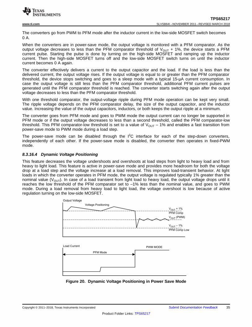
8.3.16.3 Power-Save Mode and Pulse-Frequency Modulation (PFM)By default, all three DC/DC converters go to pulse-frequency modulation (PFM) mode at light loads, and fixed-frequency pulse-width modulation (PWM) mode at heavy loads. In some applications, forcing PWM operationeven at light loads is required, which is done by setting the PFM_ENx bits in the DEFSLEW registers to 1b(default setting is 0b). In PFM mode, the converter skips switching cycles and operates with decreased frequencywith a minimum quiescent current to keep high efficiency. The converter positions the output voltage typically 1%above the nominal output voltage. This voltage-positioning feature minimizes the voltage drop caused by asudden load step.
The converters go from PWM to PFM mode after the inductor current in the low-side MOSFET switch becomes0 A.
When the converters are in power-save mode, the output voltage is monitored with a PFM comparator. As theoutput voltage decreases to less than the PFM comparator threshold of VOUT + 1%, the device starts a PFMcurrent pulse. Starting the pulse is done by turning on the high-side MOSFET and ramping up the inductorcurrent. Then the high-side MOSFET turns off and the low-side MOSFET switch turns on until the inductorcurrent becomes 0 A again.
The converter effectively delivers a current to the output capacitor and the load. If the load is less than thedelivered current, the output voltage rises. If the output voltage is equal to or greater than the PFM comparatorthreshold, the device stops switching and goes to a sleep mode with a typical 15-µA current consumption. Incase the output voltage is still less than the PFM comparator threshold, additional PFM current pulses aregenerated until the PFM comparator threshold is reached. The converter starts switching again after the outputvoltage decreases to less than the PFM comparator threshold.
With one threshold comparator, the output-voltage ripple during PFM mode operation can be kept very small.The ripple voltage depends on the PFM comparator delay, the size of the output capacitor, and the inductorvalue. Increasing the value of the output capacitors, inductors, or both keeps the output ripple at a minimum.
The converter goes from PFM mode and goes to PWM mode the output current can no longer be supported inPFM mode or if the output voltage decreases to less than a second threshold, called the PFM comparator-lowthreshold. This PFM comparator-low threshold is set to a value of VOUT – 1% and enables a fast transition frompower-save mode to PWM mode during a load step.
The power-save mode can be disabled through the I2C interface for each of the step-down converters,independently of each other. If the power-save mode is disabled, the converter then operates in fixed-PWMmode.
8.3.16.4 Dynamic Voltage PositioningThis feature decreases the voltage undershoots and overshoots at load steps from light to heavy load and fromheavy to light load. This feature is active in power-save mode and provides more headroom for both the voltagedrop at a load step and the voltage increase at a load removal. This improves load-transient behavior. At lightloads in which the converter operates in PFM mode, the output voltage is regulated typically 1% greater than thenominal value (VOUT). In case of a load transient from light load to heavy load, the output voltage drops until itreaches the low threshold of the PFM comparator set to –1% less than the nominal value, and goes to PWMmode. During a load removal from heavy load to light load, the voltage overshoot is low because of activeregulation turning on the low-side MOSFET.
Figure 20. Dynamic Voltage Positioning in Power Save Mode
8.3.16.5 100% Duty-Cycle Low-Dropout OperationThe converter starts to go to the 100% duty-cycle mode after the input voltage (VIN) comes close to the nominaloutput voltage. To keep the output voltage steady, the high-side MOSFET is turned on 100% for one or morecycles. As the VIN voltage decreases further, the high-side MOSFET is turned on completely. In this case, theconverter offers a low input-to-output voltage difference which is particularly useful in battery-poweredapplications to achieve longest operation time by taking full advantage of the whole battery voltage range.
Use Equation 2 to calculate the minimum input voltage to keep regulation (VIN,MIN) which depends on the loadcurrent and output voltage.
where• VOUT,MAX is the nominal output voltage plus the maximum output voltage tolerance.• IOUT,MAX the maximum output current plus the inductor ripple current.• RDSON,MAX is the maximum upper MOSFET switch RDSON resistance.• RL is the DC resistance of the inductor. (2)
8.3.16.6 Short-Circuit ProtectionHigh-side and low-side MOSFET switches are short-circuit protected. After the high-side MOSFET switchreaches its current limit, it is turned off and the low-side MOSFET switch is turned on. The high-side MOSFETswitch can only turn on again after the current in the low-side MOSFET switch decreases to less than its currentlimit.
8.3.16.7 Soft StartThe three step-down converters in the TPS65217x device have an internal soft-start circuit that controls theramp-up of the output voltage. The output voltage ramps up from 5% to 95% of its nominal value within 750 µs.This ramp up limits the inrush current in the converter during start-up and prevents possible input voltage dropswhen a battery or high-impedance power source is used. The soft-start circuit is enabled after the start-up time,tStart, expires.
Figure 21. Output of the DC/DC Converters is Ramped Up Within 750 µs
8.3.17 Standby LDO Regulators (LDO1, LDO2)The LDO1 and LDO2 regulators support up to 100 mA each, are internally current limited, and have a maximumdropout voltage of 200 mV at the rated output current. In SLEEP mode, however, the output current is limited to1 mA each. When disabled, both outputs are discharged to ground through a 430-Ω resistor.
The LDO1 regulator supports an output voltage range from 1 V to 1.8 V, which is controlled through theDEFLDO1 register. The LDO2 regulator supports an output voltage range from 0.9 V to 1.5 V, and is controlledthrough the DEFLDO2 register. By default, the LDO1 regulator is enabled immediately after a power-up event asdescribed in the PMIC States section and stays on in the SLEEP state to support system standby. Each LDOregulator has low standby current of less than 15 µA (typical).
The LDO2 regulator can be configured to track the output voltage of the DCDC3 converter (core voltage). Whenthe TRACK bit is set to 1b in the DEFLDO2 register, the output is determined by the DCDC3[5:0] bits of theDEFDCDC3 register and the LDO2[5:0] bits of the DEFLDO2 register are ignored.
The LDO1 and LDO2 regulators can be controlled through STROBE 1 through 6, special STROBES 14 and 15,or through the corresponding enable bits in the ENABLE register. By default, the LDO1 regulator is controlled bySTROBE 15, which keeps LDO1 on in the SLEEP state. The STROBE assignments can be changed by the userwhile the device is in the ACTIVE state, but all register settings are reset to the default values when the devicegoes to the SLEEP or OFF state. TI does not recommend real-time modification of the STROBE assignments ofthe LDO1 or LDO2 regulator. For permanent changes to the default STROBE assignments, custom programmingduring production at the TI factory is required.
8.3.18 Load Switches or LDO Regulators (LS1 or LDO3, LS2 or LDO4)The TPS65217x device has two general-purpose load switches that can also be configured as LDOs. As LDOs,they support up to 200 mA (TPS65217B) or 400 mA (TPS65217C and TPS65217D) each, are internally current-limited, and have a maximum dropout voltage of 200 mV at rated output current. These two outputs areconfigured as LS1 and LS2 load switched in the TPS65217A variant of the device. The on-off state of the loadswitches (LS1 and LS2) or the LDO regulators (LDO3 and LDO4) is controlled either through the sequencer orthe LS1_EN and LS2_EN bits of the ENABLE register. When disabled, both outputs are discharged to groundthrough a 375-Ω resistor.
Configured as load switches, LS1 and LS2 have a maximum impedance of 650 mΩ. Different from LDOoperation, load switches can stay in current limit indefinitely without affecting the internal power-good signal oraffecting the other rails.
NOTEExcessive power dissipation in the switches may cause thermal shutdown of the device.
Load switch and LDO modes are controlled by the LS1LDO3 and LS2LDO4 bits of the DEFLS1 and DEFLS2registers.
8.3.19 White LED DriverThe TPS65217x device has a boost converter and two current sinks capable of driving two strings containing upto 10 LEDs in each string (also known as a 2 × 10 matrix) LEDs at 25 mA or one string of up to 10 LEDs at 50mA of current. Use Equation 3 to calculate the current of each current sink.
(3)
Two different current levels can be programmed using two external RSET resistors. Only one current setting isactive at any given time, and both current sinks are always regulated to the same current. The active currentsetting is selected through the ISEL bit of the WLEDCTRL1 register.
An internal PWM signal and I2C control support brightness and dimming. Both current sources are controlledtogether and cannot operate independently. By default, the PWM frequency is set to 200 Hz, but can be changedto 100 Hz, 500 Hz, or 1000 Hz. The PWM duty cycle can be adjusted from 1% (default) to 100% in 1% stepsthrough the WLEDCTRL2 register.
When the ISINK_EN bit of WLEDCTRL1 register is set to 1b, both current sinks are enabled, and the boostoutput voltage at the FB_WLED pin is regulated to support the same sink current through each current sink. Theboost output voltage, however, is internally limited to 39 V.
If only one WLED string is required, short the ISINK1 and ISINK2 pins together and connect them to the cathodeof the diode string. In this case, the LED current two times the sink current. Figure 22 shows the basic schematicand internal circuitry of the WLED driver used to drive two strings. Figure 23 shows the basic schematic andinternal circuitry of the WLED driver used to one string. Table 33 and Table 34 list the recommended inductorsand output capacitors for the WLED boost converters.
Figure 22. Block Diagram of WLED Driver—Dual-String Operation
This operation has the same LED current as dual-string operation. For single-string operation, both ISINK pins areshorted together and the RSET resistor values (R1 and R2) are doubled to halve the current that each ISINKx pinpulls, resulting in the same current through the LEDs as in dual-string operation.
Figure 23. Block Diagram of WLED Driver—Single-String Operation
(1) Only if USB or AC supply is present(2) Rails are powered-down as controlled by the sequencer in default EEPROM settings(3) Battery voltage always supplies the system (from BAT pin to SYS pin)(4) LDO1 is assigned to STROBE15 in default EEPROM settings and this special strobe is not controlled by the
sequencer. LDO1 can only source 1 mA in the SLEEP state(5) The 9-MHz oscillator is enabled only when WLED or DCDC or PPATH or CHARGER is enabled.(6) The charger, auto-discharge, PPATH, and 9-MHz oscillator are ON in the SLEEP state if AC or USB is present and
the charger is enabled and not fully charged.(7) Any USB = 1(↑) or AC = 1 (↑) event in the WAIT MIN OFF TIME2 state makes the device go from the SLEEP state
when the timer expires. Any USB = 1(↑) or AC = 1 (↑) event in the WAIT MIN OFF TIME3 state makes the device gofrom the PRE-OFF state when the timer expires.
(8) All user registers are reset to default values each time the device goes to the SLEEP state.(9) UVLO and OTS are monitored in all the states except the OFF, POR, and WAIT DEGLITCH states.
Device Functional Modes (continued)8.4.1 PMIC States
8.4.1.1 OFF StateIn the OFF state, the PMIC is completely shut down with the exception of a few circuits to monitor the voltage onthe AC, USB, and PB_IN pins. All output power rails are turned off and the registers are reset to their defaultvalues. The I2C communication interface is turned off. The lowest amount of power is used in this state. To exitthe OFF state, one of the following wake-up events must occur:• The PB_IN pin is pulled low.• The USB supply is connected (positive edge).• The AC adapter is connected (positive edge).
To go to the OFF state, set the OFF bit in the STATUS register to 1b, and then pull the PWR_EN pin low. Innormal operation, the device can only go to the OFF state from the ACTIVE state. Whenever a fault occursduring operation, such as thermal shutdown, power-good fail, undervoltage lockout, or a PWR_EN pin timeout,all power rails are shut down and the device goes to the OFF state. The device stays in the OFF state until thefault is removed then a new power-up event occurs.
8.4.1.2 ACTIVE StateThis state is the typical mode of operation when the system is up and running. All DC/DC converters, LDOregulators, load switches, the WLED driver, and the battery charger are operational and can be controlledthrough the I2C interface.
After a wake-up event, the PMIC enables all rails not controlled by the sequencer and pulls the nWAKEUP pinlow to signal the event to the host processor. The device goes to the ACTIVE state only if the host asserts thePWR_EN pin within 5 s after the wake-up event. Otherwise, the device goes to the OFF state. In the ACTIVEstate, the sequencer is triggered to automatically enable the remaining power rails. The nWAKEUP pin returns tothe Hi-Z state after the PWR_EN pin has been asserted. Figure 3 shows a timing diagram. The device can alsogo directly to the ACTIVE state from the SLEEP state by pulling the PWR_EN pin high. For more information,see the description of the SLEEP State.
The PWR_EN pin must be pulled low for the device to go from ACTIVE state.
8.4.1.3 SLEEP StateThe SLEEP state is a low-power mode of operation intended to support system standby. Typically, all power railsare turned off with the exception of the LDO1 rail, and the registers are reset to their default values. The LDO1rail stays operational but can support only a limited amount of current (1 mA typical).
To go to the SLEEP state, set the OFF bit in the STATUS register to 0b (default), and then pull the PWR_EN pinlow. All power rails controlled by the power-down sequencer are shut down, and after 1 s the device goes to theSLEEP state. If the LDO1 rail was enabled in the ACTIVE state, the LDO1 rail stays enabled in the SLEEP sate.All rails not controlled by the power-down sequencer also keep state. The battery charger stays active for as longas either the USB or AC supply is connected to the device. All register values are reset when the device goes tothe SLEEP state, including charger parameters.
The device goes to the ACTIVE state after detecting a wake-up event as described in the previous sections. Inaddition, the device goes from the SLEEP to the ACTIVE state when the PWR_EN pin is pulled high. The systemhost can go between the ACTIVE and SLEEP states by control of the PWR_EN pin only. This feature bypassesthe requirement for a wake-up event from an external source to occur.
Device Functional Modes (continued)8.4.1.4 RESET StateThe TPS65217x device can be reset by either pulling the nRESET pin low or by holding the PB_IN pin low formore than 8 s. All rails are shut down by the sequencer and all register values are reset to their default values.Rails not controlled by the sequencer are shut down after the power-down sequencer is complete. The devicestays in the this state for as long as the reset pin is held low, and the nRESET pin must be high for the device togo from the RESET state. However, the device stays in the RESET state for a minimum of 1 s before going backto the ACTIVE state. As detailed in the description of the ACTIVE State, the PWR_EN pin must be assertedwithin 5 s of the nWAKEUP pin going low for the device to go to the ACTIVE state. The RESET function power-cycles the device and only shuts down the output rails temporarily. Resetting the device does put the device inthe OFF state.
If the PB_IN pin is kept low for an extended amount of time, the device continues to cycle between the ACTIVEand RESET states, and goes to the RESET state after each 8-s time period.
8.5 Programming
8.5.1 I2C Bus OperationThe TPS65217x device hosts a slave I2C interface that is compliant with I2C standard 3.0 and supports datarates up to 400 kbit/s and auto-increments addressing.
Figure 25. Subaddress in I2C Transmission
The I2C bus is a communications link between a controller and a series of slave terminals. The link is establishedusing a two-wire bus consisting of a serial clock signal (SCL) and a serial data signal (SDA). The serial clock issourced from the controller in all cases, where the serial data line is bidirectional for data communicationbetween the controller and the slave terminals. Each device has an open-drain output to transmit data on theserial data line. An external pullup resistor must be placed on the serial data line to pull the drain output highduring data transmission.
Data transmission is initiated with a start bit from the controller as shown in Figure 28. The start condition isrecognized when the SDA line goes from high to low during the high portion of the SCL signal. On reception of astart bit, the device receives serial data on the SDA input and checks for valid address and control information. Ifthe appropriate group and address bits are set for the device, then the device issues an acknowledge (ACK)pulse and prepares for the reception of subaddress data. Subaddress data is decoded and responded toaccording to the Register Maps. Data transmission is completed by either the reception of a stop condition or thereception of the data word sent to the device. A stop condition is recognized as a low-to-high transition of theSDA input during the high portion of the SCL signal. All other transitions of the SDA line must occur during thelow portion of the SCL signal. An acknowledge is issued after the reception of a valid address, subaddress, anddata words. The I2C interface auto-sequences through the register addresses, so that multiple data words can besent for a given I2C transmission. For details, see Figure 26, Figure 27, and Figure 28.
Programming (continued)8.5.2 Password ProtectionRegisters 0x0B through 0x1F, with the exception of the password register, are protected against accidentalwriting by an 8-bit password. The password must be written before writing to a protected register and isautomatically reset to 0x00 after the following I2C transaction, regardless of the register that was accessed andregardless of the transaction type (read or write). The password is required for write access only and is notrequired for read access.
8.5.2.1 Level1 ProtectionTo write to a Level1 protected register, follow these steps:1. Write the address of the destination register, XORed with the protection password (0x7D) to the
PASSWORD register.2. Write data to the password-protected register.3. Data is only transferred to the protected register if the content of the PASSWORD register XORed with the
address sent in Step 2 matches 0x7D. Otherwise, the transaction is ignored. The PASSWORD register isreset to 0x00 after the transaction regardless of whether the XOR logical function matched 0x7D or not.
The cycle must be repeated for any other register that is Level1 write protected.
8.5.2.2 Level2 ProtectionTo write to a Level2 protected register, follow these steps:1. Write the address of the destination register, XORed with the protection password (0x7D) to the
PASSWORD register.2. Write data to the password-protected register.3. The data is temporarily stored if the content of the PASSWORD register XORed with the address sent in
Step 2 matches 0x7D. The register value does not change at this point, but the PASSWORD register is resetto 0x00 after the transaction regardless of whether the XOR logical function matched 0x7D or not.
4. Write the address of the destination register, XORed with the protection password (0x7D) to thePASSWORD register.
5. Write the same data as in Step 2 to the password protected register.6. The content of the PASSWORD register is XORed again with the address sent in Step 5 must match 0x7D
for the data to be valid.7. The register is updated only if both data transfers in Step 2 and Step 5 were valid, and the transferred data
matched.
NOTENo other I2C transaction can occur between Step 2 and Step 5, and the register is notupdated if any other transaction occurs between Step 2 and Step 5. The cycle must berepeated for any other register that is Level2 write protected.
8.5.3 Resetting of Registers to Default ValuesAll registers are reset to default values when one or more of the following conditions occur:• The device goes from the ACTIVE state to the SLEEP state or OFF state.• The BAT or USB supply is applied from a power-less state (power-on reset).• The push-button input is pulled low for more than 8 s.• The nRESET pin is pulled low.• A fault occurs.
8.6.1 Register Address MapFigure 29 lists the memory-mapped registers for the device registers. All register offset addresses not listed inshould be considered as reserved locations and the register contents should not be modified.
Figure 29. Register Address Map
Address(Decimal)
Address(Hexadecimal) Name Password
Protection LevelDefaultValue Description Section
0 0x00 CHIPID None X Chip ID Go
1 0x01 PPATH None 0x3D Power path control Go
2 0x02 INT None 0x80 Interrupt flags and masks Go
3 0x03 CHGCONFIG0 None 0x00 Charger control register 0 Go
4 0x04 CHGCONFIG1 None 0xB1 Charger control register 1 Go
5 0x05 CHGCONFIG2 None 0x80 Charger control register 2 Go
6 0x06 CHGCONFIG3 None 0xB2 Charger control register 3 Go
7 0x07 WLEDCTRL1 None 0xB1 WLED control register Go
8 0x08 WLEDCTRL2 None 0x00 WLED PWM duty cycle Go
9 0x09 MUXCTRL None 0x00 Analog multiplexer control register Go
10 0x0A STATUS None 0x00 Status register Go
11 0x0B PASSWORD None 0x00 Write password Go
12 0x0C PGOOD None 0x00 Power good (PG) flags Go
13 0x0D DEFPG Level1 0x0C Power good (PG) delay Go
14 0x0E DEFDCDC1 Level2 X DCDC1 voltage adjustment Go
15 0x0F DEFDCDC2 Level2 X DCDC2 voltage adjustment Go
16 0x10 DEFDCDC3 Level2 0x08 DCDC3 voltage adjustment Go
17 0x11 DEFSLEW Level2 0x06 Slew control for DCDC1, DCDC2, DCDC3, andPFM mode enable Go
18 0x12 DEFLDO1 Level2 0x09 LDO1 voltage adjustment Go
19 0x13 DEFLDO2 Level2 0x38 LDO2 voltage adjustment Go
20 0x14 DEFLS1 Level2 X LS1 or LDO3 voltage adjustment Go
21 0x15 DEFLS2 Level2 X LS2 or LDO4 voltage adjustment Go
22 0x16 ENABLE Level1 0x00 Enable register Go
23 0x18 DEFUVLO Level1 0x03 UVLO control register Go
24 0x19 SEQ1 Level1 X Power-up STROBE definition Go
25 0x1A SEQ2 Level1 X Power-up STROBE definition Go
26 0x1B SEQ3 Level1 X Power-up STROBE definition Go
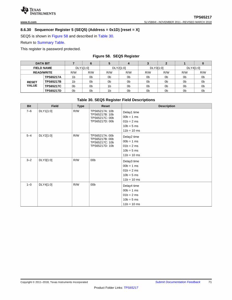
27 0x1C SEQ4 Level1 0x40 Power-up STROBE definition Go
28 0x1D SEQ5 Level1 X Power-up delay times Go
29 0x1E SEQ6 Level1 0x00 Power-up delay times Go
Bit access types are abbreviated to fit into small table cells. Table 1 shows the abbreviation codes that are usedfor access types in this section. Registers that are different for each TPS65217x variant will have differenthexadecimal reset values and are shown as X. The hexadecimal reset value can de determined by convertingthe binary reset value.
(1) Reserved bits can be R or R/W. Read-only (R) Reserved bits are not used and writing data to thesebits will have no effect on device operation. Read and Write (R/W) Reserved bits are settings thatcannot be modified. The reset value must always be written to these bits. Modifying a R/W Reservedbit will have an impact on device operation and can produce unwanted device behavior.
Table 1. Access Type CodesAccess Type (1) Code DescriptionRead R Read-onlyRead/Write R/W Read and Write
8.6.3 Power Path Control Register (PPATH) (Address = 0x01) [reset = 0x3D]PPATH is shown in Figure 31 and described in Table 3.
Return to Summary Table.
Figure 31. PPATH Register
DATA BIT 7 6 5 4 3 2 1 0FIELD NAME ACSINK USBSINK AC_EN USB_EN IAC[1:0] IUSB[1:0]READ/WRITE R/W R/W R/W R/W R/W R/W R/W R/W
RESET VALUE 0b 0b 1b 1b 1b 1b 0b 1b
Table 3. PPATH Register Field DescriptionsBit Field Type Reset Description7 ACSINK R/W 0b AC current-sink control
NOTE: [ACSINK, USBSINK] = 01b and 10b combinations arenot recommended, as these may lead to unexpected enablingand disabling of the current sinks.0b = AC sink is enabled when USB is a valid supply and VAC isless than the detection threshold1b = Set ACSINK and USBSINK to 1b at the same time to forceboth (AC and USB) current sinks OFF
6 USBSINK R/W 1b USB current-sink controlNOTE: [ACSINK, USBSINK] = 01b and 10b combinations arenot recommended, as these may lead to unexpected enablingand disabling of the current sinks.0b = USB sink is enabled when AC is a valid supply and VUSB isless than the detection threshold1b = Set ACSINK and USBSINK to 1b at the same time to forceboth (AC and USB) current sinks OFF
5 AC_EN R/W 1b AC power path enable0b = AC power input is turned off.1b = AC power input is turned on.
4 USB_EN R/W 1b USB power path enable0b = USB power input is turned off (USB suspend mode).1b = USB power input is turned on.
3–2 IAC[1:0] R/W 11b AC input-current limit00b = 100 mA01b = 500 mA10b = 1300 mA11b = 2500 mA
1–0 IUSB[1:0] R/W 01b USB input-current limit00b = 100 mA01b = 500 mA10b = 1300 mA11b = 1800 mA
8.6.4 Interrupt Register (INT) (Address = 0x02) [reset = 0x80]INT is shown in Figure 32 and described in Table 4.
Return to Summary Table.
Figure 32. INT Register
DATA BIT 7 6 5 4 3 2 1 0FIELD NAME Reserved PBM ACM USBM Reserved PBI ACI USBIREAD/WRITE R/W R/W R/W R/W R R R R
RESET VALUE 1b 0b 0b 0b 0b 0b 0b 0b
Table 4. INT Register Field DescriptionsBit Field Type Reset Description7 Reserved R/W 1b This bit is reserved6 PBM R/W 0b Push-button status change interrupt mask
0b = Interrupt is issued when PB status changes.1b = No interrupt is issued when PB status changes.
5 ACM R/W 0b AC interrupt mask0b = Interrupt is issued when power to the AC input is applied orremoved.1b = No interrupt is issued when power to the AC input isapplied or removed.
4 USBM R/W 0b USB power status change interrupt mask0b = Interrupt is issued when power to USB input is applied orremoved.1b = No interrupt is issued when power to USB input is appliedor removed.
3 Reserved R 0b This bit is reserved2 PBI R 0b Push-button status change interrupt
NOTE: Status information is available in the STATUS register.0b = No change in status1b = Push-button status change (PB_IN changed high to low orlow to high)
1 ACI R 0b AC power status change interruptNOTE: Status information is available in the STATUS register.0b = No change in status1b = AC power status change (power to the AC pin has eitherbeen applied or removed)
0 USBI R 0b USB power status change interruptNOTE: Status information is available in the STATUS register.0b = No change in status1b = USB power status change (power to the USB pin has eitherbeen applied or removed)
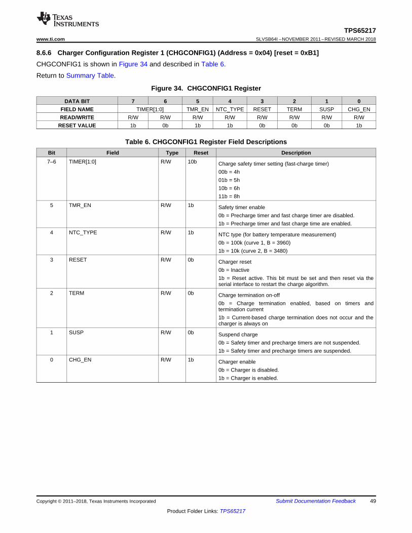
8.6.5 Charger Configuration Register 0 (CHGCONFIG0) (Address = 0x03) [reset = 0x00]CHGCONFIG0 is shown in Figure 33 and described in Table 5.
Return to Summary Table.
Figure 33. CHGCONFIG0 Register
DATA BIT 7 6 5 4 3 2 1 0FIELD NAME TREG DPPM TSUSP TERMI ACTIVE CHGTOUT PCHGTOUT BATTEMPREAD/WRITE R R R R R R R R
RESET VALUE 0b 0b 0b 0b 0b 0b 0b 0b
Table 5. CHGCONFIG0 Register Field DescriptionsBit Field Type Reset Description7 TREG R 0b Thermal regulation
0b = Charger is in normal operation.1b = Charge current is reduced because of high chiptemperature.
6 DPPM R 0b DPPM active0b = DPPM loop is not active.1b = DPPM loop is active; charge current is reduced to supportthe load with the current required.
5 TSUSP R 0b Thermal suspend0b = Charging is allowed.1b = Charging is temporarily suspended because batterytemperature is out of range.
4 TERMI R 0b Termination current detect0b = Charging, charge termination current threshold has notbeen crossed.1b = Charge termination current threshold has been crossed andcharging has been stopped. This can be from a battery reachingfull capacity or to a battery removal condition.
3 ACTIVE R 0b Charger active bit0b = Charger is not charging.1b = Charger is charging (DPPM or thermal regulation may beactive).
2 CHGTOUT R 0b Charge timer time-out0b = Charging, timers did not time out.1b = One of the timers has timed out and charging has beenterminated.
1 PCHGTOUT R 0b Precharge timer time-out0b = Charging, precharge timer did not time out.1b = Precharge timer has timed out and charging has beenterminated.
0 BATTEMP R 0b Battery temperature and NTC errorNOTE: This bit does not indicate that the battery temperature iswithin the valid range for charging.0b = Battery temperature is in the allowed range for charging.1b = No temperature sensor detected or battery temperatureoutside valid charging range
8.6.6 Charger Configuration Register 1 (CHGCONFIG1) (Address = 0x04) [reset = 0xB1]CHGCONFIG1 is shown in Figure 34 and described in Table 6.
Return to Summary Table.
Figure 34. CHGCONFIG1 Register
DATA BIT 7 6 5 4 3 2 1 0FIELD NAME TIMER[1:0] TMR_EN NTC_TYPE RESET TERM SUSP CHG_ENREAD/WRITE R/W R/W R/W R/W R/W R/W R/W R/W
RESET VALUE 1b 0b 1b 1b 0b 0b 0b 1b
Table 6. CHGCONFIG1 Register Field DescriptionsBit Field Type Reset Description7–6 TIMER[1:0] R/W 10b Charge safety timer setting (fast-charge timer)
00b = 4h01b = 5h10b = 6h11b = 8h
5 TMR_EN R/W 1b Safety timer enable0b = Precharge timer and fast charge timer are disabled.1b = Precharge timer and fast charge time are enabled.
4 NTC_TYPE R/W 1b NTC type (for battery temperature measurement)0b = 100k (curve 1, B = 3960)1b = 10k (curve 2, B = 3480)
3 RESET R/W 0b Charger reset0b = Inactive1b = Reset active. This bit must be set and then reset via theserial interface to restart the charge algorithm.
2 TERM R/W 0b Charge termination on-off0b = Charge termination enabled, based on timers andtermination current1b = Current-based charge termination does not occur and thecharger is always on
1 SUSP R/W 0b Suspend charge0b = Safety timer and precharge timers are not suspended.1b = Safety timer and precharge timers are suspended.
0 CHG_EN R/W 1b Charger enable0b = Charger is disabled.1b = Charger is enabled.
8.6.9 WLED Control Register 1 (WLEDCTRL1) (Address = 0x07) [reset = 0xB1]WLEDCTRL1 is shown in Figure 37 and described in Table 9.
Return to Summary Table.
Figure 37. WLEDCTRL1 Register
DATA BIT 7 6 5 4 3 2 1 0
FIELD NAME Reserved Reserved Reserved Reserved ISINK_EN ISEL FDIM[1:0]
READ/WRITE R R R R R/W R/W R/W R/W
RESET VALUE 0b 0b 0b 0b 0b 0b 0b 1b
Table 9. WLEDCTRL1 Register Field DescriptionsBit Field Type Reset Description7–4 Reserved R 0000b These bits are reserved3 ISINK_EN R/W 0b Current sink enable
NOTE: This bit enables both current sinks.0b = Current sink is disabled (OFF).1b = Current sink is enabled (ON).
2 ISEL R/W 0b ISET selection bit0b = Low-level (define by ISET1 pin)1b = High-level (defined by ISET2 pin)
8.6.11 MUX Control Register (MUXCTRL) (Address = 0x09) [reset = 0x00]MUXCTRL is shown in Figure 39 and described in Table 11.
Return to Summary Table.
Figure 39. MUXCTRL Register
DATA BIT 7 6 5 4 3 2 1 0FIELD NAME Reserved Reserved Reserved Reserved Reserved MUX[2:0]READ/WRITE R R R R R R/W R/W R/W
RESET VALUE 0b 0b 0b 0b 0b 0b 0b 0b
Table 11. MUXCTRL Register Field DescriptionsBit Field Type Reset Description7–3 Reserved R 00000b These bits are reserved2–0 MUX[2:0] R/W 000b Analog multiplexer selection
000b = MUX is disabled, output is Hi-Z.001b = VBAT010b = VSYS011b = VTS100b = VICHARGE101b = MUX_IN (external input)110b = MUX is disabled, output is Hi-Z.111b = MUX is disabled, output is Hi-Z.
8.6.12 Status Register (STATUS) (Address = 0x0A) [reset = 0x00]STATUS is shown in Figure 40 and described in Table 12.
Return to Summary Table.
Figure 40. STATUS Register
DATA BIT 7 6 5 4 3 2 1 0FIELD NAME OFF Reserved Reserved Reserved ACPWR USBPWR Reserved PBREAD/WRITE R/W R R R R R R R
RESET VALUE 0b 0b 0b 0b 0b 0b 0b 0b
Table 12. STATUS Register Field DescriptionsBit Field Type Reset Description7 OFF R/W 0b OFF bit. Set this bit to 1b to enter the OFF state when PWR_EN
pin is pulled low. The bit is automatically reset to 0b.6–4 Reserved R 000b These bits are reserved
3 ACPWR R 0b AC power status bit0b = AC power is not present and/or not in the range valid forcharging.1b = AC source is present and in the range valid for charging.
2 USBPWR R 0b USB power0b = USB power is not present and/or not in the range valid forcharging.1b = USB source is present and in the range valid for charging.
1 Reserved R 0b This bit is reserved0 PB R 0b Push Button status bit
0b = Push-button is inactive (PB_IN is pulled high).1b = Push-button is active (PB_IN is pulled low).
8.6.13 Password Register (PASSWORD) (Address = 0x0B) [reset = 0x00]PASSWORD is shown in Figure 41 and described in Table 13.
Return to Summary Table.
Figure 41. PASSWORD Register
DATA BIT 7 6 5 4 3 2 1 0FIELD NAME PWRD[7:0]READ/WRITE R/W R/W R/W R/W R/W R/W R/W R/W
RESET VALUE 0b 0b 0b 0b 0b 0b 0b 0b
Table 13. Password Register (PASSWORD) Field DescriptionsBit Field Type Reset Description7–0 PWRD[7:0] R/W 00000000b Password protection locking and unlocking
NOTE: Register is automatically reset to 0x00 after the following I2Ctransaction. See the Password Protection section for details.0000 0000b = Password-protected registers are locked for write access....0111 1100b = Password-protected registers are locked for write access.0111 1101b = Allows writing to a password-protected register in the nextwrite cycle0111 1110b = Password-protected registers are locked for write access....1111 1111b = Password-protected registers are locked for write access.
8.6.15 Power-Good Control Register (DEFPG) (Address = 0x0D) [reset = 0x0C]DEFPG is shown in Figure 43 and described in Table 15.
Return to Summary Table.
This register is password protected.
Figure 43. DEFPG Register
DATA BIT 7 6 5 4 3 2 1 0
FIELD NAME Reserved Reserved Reserved Reserved LDO1PGM LDO2PGM PGDLY[1:0]
READ/WRITE R R R R R/W R/W R/W R/W
RESET VALUE 0b 0b 0b 0b 1b 1b 0b 0b
Table 15. DEFPG Register Field DescriptionsBit Field Type Reset Description7–4 Reserved R 0000b These bits are reserved3 LDO1PGM R/W 1b LDO1 power-good masking bit
0b = PGOOD pin is pulled low if LDO1_PG is low1b = LDO1_PG status does not affect the status of the PGOODoutput pin.
2 LDO2PGM R/W 1b LDO2 power-good masking bit0b = PGOOD pin is pulled low if LDO2_PG is low1b = LDO2_PG status does not affect the status of the PGOODoutput pin.
1–0 PGDLY[1:0] R/W 00b Power-good delayNOTE: PGDLY applies to the PGOOD pin.00b = 20 ms01b = 100 ms10b = 200 ms11b = 400 ms
8.6.19 Slew-Rate Control Register (DEFSLEW) (Address = 0x11) [reset = 0x06]DEFSLEW is shown in Figure 47 and described in Table 19.
Return to Summary Table.
Slew-rate control applies to all three DC/DC converters.This register is password protected.
Figure 47. DEFSLEW Register
DATA BIT 7 6 5 4 3 2 1 0FIELD NAME GO GODSBL PFM_EN1 PFM_EN2 PFM_EN3 SLEW[2:0]READ/WRITE R/W R/W R/W R/W R/W R/W R/W R/W
RESET VALUE 0b 0b 0b 0b 0b 1b 1b 0b
Table 19. DEFSLEW Register Field DescriptionsBit Field Type Reset Description7 GO R/W 0b Go bit
NOTE: Bit is automatically reset at the end of the voltagetransition.0b = No change1b = Initiates the transition from the present state to the outputvoltage setting currently stored in the DEFDCDCx register
6 GODSBL R/W 0b Go Disable bit0b = Enabled1b = Disabled; DCDCx output voltage changes wheneversetpoint is updated in DEFDCDCx register without having towrite to the GO bit. SLEW[2:0] setting does apply.
5 PFM_EN1 R/W 0b PFM enable bit, DCDC10b = DC/DC converter operates in the PWM or PFM mode,depending on load.1b = DC/DC converter is forced into the fixed-frequency PWMmode.
4 PFM_EN2 R/W 0b PFM enable bit, DCDC20b = DC/DC converter operates in the PWM or PFM mode,depending on load.1b = DC/DC converter is forced into the fixed-frequency PWMmode.
3 PFM_EN3 R/W 0b PFM enable bit, DCDC30b = DC/DC converter operates in the PWM or PFM mode,depending on load.1b = DC/DC converter is forced into the fixed-frequency PWMmode.
2–0 SLEW[2:0] R/W 0110b Output slew-rate settingNOTE: The actual slew rate depends on the voltage step percode. See the DCDC1 and DCDC2 registers for details.000b = 224 µs/step (0.11 mV/µs at 25 mV per step)001b = 112 µs/step (0.22 mV/µs at 25 mV per step)010b = 56 µs/step (0.45 mV/µs at 25 mV per step)011b = 28 µs/step (0.90 mV/µs at 25 mV per step)100b = 14 µs/step (1.80 mV/µs at 25 mV per step)101b = 7 µs/step (3.60 mV/µs at 25 mV per step)110b = 3.5 µs/step (7.2 mV/µs at 25 mV per step)111b = Immediate; slew rate is only limited by the control loopresponse time.
8.6.20 LDO1 Control Register (DEFLDO1) (Address = 0x12) [reset = 0x09]DEFLDO1 is shown in Figure 48 and described in Table 20.
Return to Summary Table.
This register is password protected.
Figure 48. DEFLDO1 Register
DATA BIT 7 6 5 4 3 2 1 0FIELD NAME Reserved Reserved Reserved Reserved LDO1[3:0]READ/WRITE R R R R R/W R/W R/W R/W
RESET VALUE 0b 0b 0b 0b 1b 0b 0b 1b
Table 20. DEFLDO1 Register Field DescriptionsBit Field Type Reset Description7–4 Reserved R 0000b These bits are reserved3–0 LDO1[3:0] R/W 1001b LDO1 output voltage setting
8.6.24 Enable Register (ENABLE) (Address = 0x16) [reset = 0x00]ENABLE is shown in Figure 52 and described in Table 24.
Return to Summary Table.
This register is password protected.
Figure 52. ENABLE Register
DATA BIT 7 6 5 4 3 2 1 0FIELD NAME Reserved LS1_EN LS2_EN DC1_EN DC2_EN DC3_EN LDO1_EN LDO2_ENREAD/WRITE R R/W R/W R/W R/W R/W R/W R/W
RESET VALUE 0b 0b 0b 0b 0b 0b 0b 0b
Table 24. ENABLE Register Field DescriptionsBit Field Type Reset Description7 Reserved R 0b This bit is reserved6 LS1_EN R/W 0b LSW1 or LDO3 enable bit
NOTE: PWR_EN pin must be high to enable LS1 or LDO3.0b = Disabled1b = Enabled
5 LS2_EN R/W 0b LS2 or LDO4 enable bitNOTE: PWR_EN pin must be high to enable LS2 or LDO4.0b = Disabled1b = Enabled
4 DC1_EN R/W 0b DCDC1 enable bitNOTE: PWR_EN pin must be high to enable the DC/DCconverter.0b = DCDC1 is disabled.1b = DCDC1 is enabled.
3 DC2_EN R/W 0b DCDC2 enable bitNOTE: PWR_EN pin must be high to enable the DC/DCconverter.0b = DCDC2 is disabled.1b = DCDC2 is enabled.
2 DC3_EN R/W 0b DCDC3 enable bitNOTE: PWR_EN pin must be high to enable the DC/DCconverter.0b = DCDC3 is disabled.1b = DCDC3 is enabled.
8.6.25 UVLO Control Register (DEFUVLO) (Address = 0x18) [reset = 0x03]DEFUVLO is shown in Figure 53 and described in Table 25.
Return to Summary Table.
This register is password protected.
Figure 53. DEFUVLO Register
DATA BIT 7 6 5 4 3 2 1 0
FIELD NAME Reserved Reserved Reserved Reserved Reserved Reserved UVLO[1:0]
READ/WRITE R R R R R R/W R/W R/W
RESET VALUE 0b 0b 0b 0b 0b 0b 1b 1b
Table 25. DEFUVLO Register Field DescriptionsBit Field Type Reset Description7–3 Reserved R 00000b These bits are reserved2 Reserved R/W 0b This bit is reserved
DCDC1 enable STROBE0000b = Rail is not controlled by sequencer.0001b = Enable at STROBE10010b = Enable at STROBE20011b = Enable at STROBE30100b = Enable at STROBE40101b = Enable at STROBE50110b = Enable at STROBE60111b = Enable at STROBE7
3 Reserved R 0b This bit is reserved2–0 DC2_SEQ[3:0] R/W TPS65217A: 0010b
TPS65217B: 0101bTPS65217C: 0101bTPS65217D: 0101b
DCDC2 enable STROBE0000b = Rail is not controlled by sequencer.0001b = Enable at STROBE10010b = Enable at STROBE20011b = Enable at STROBE30100b = Enable at STROBE40101b = Enable at STROBE50110b = Enable at STROBE60111b = Enable at STROBE7
DCDC3 enable STROBE000b = Rail is not controlled by sequencer.001b = Enable at STROBE1010b = Enable at STROBE2011b = Enable at STROBE3100b = Enable at STROBE4101b = Enable at STROBE5110b = Enable at STROBE6111b = Enable at STROBE7
LDO1 enable state0000b = Rail is not controlled by sequencer.0001b = Enable at STROBE10010b = Enable at STROBE20011b = Enable at STROBE30100b = Enable at STROBE40101b = Enable at STROBE50110b = Enable at STROBE60111b = Enable at STROBE71000b = Rail is not controlled by sequencer1001b = Rail is not controlled by sequencer1010b to 1101b = Reserved1110b = Enable at STROBE141111b = Enabled at STROBE15 (with SYS)
Table 28. SEQ3 Register Field DescriptionsBit Field Type Reset Description7–4 LDO2_SEQ[3:0] R/W TPS65217A: 0010b
TPS65217B: 0010bTPS65217C: 0011bTPS65217D: 0011b
LDO2 enable STROBE0000b = Rail is not controlled by sequencer.0001b = Enable at STROBE10010b = Enable at STROBE20011b = Enable at STROBE30100b = Enable at STROBE40101b = Enable at STROBE50110b = Enable at STROBE60111b = Enable at STROBE71000b = Rail is not controlled by sequencer.1001b = Rail is not controlled by sequencer.1010b to 1101b = Reserved1110b = Enable at STROBE141111b = Enabled at STROBE15 (with SYS)
3 Reserved R 0b This bit is reserved2–0 LDO3_SEQ[2:0] R/W TPS65217A: 001b
TPS65217B: 011bTPS65217C: 010bTPS65217D: 010b
LS1 or LDO3 enable state000b = Rail is not controlled by sequencer001b = Enable at STROBE1010b = Enable at STROBE2011b = Enable at STROBE3100b = Enable at STROBE4101b = Enable at STROBE5110b = Enable at STROBE6111b = Enable at STROBE7
8.6.29 Sequencer Register 4 (SEQ4) (Address = 0x1C) [reset = 0x40]SEQ4 is shown in Figure 57 and described in Table 29.
Return to Summary Table.
This register is password protected.
Figure 57. SEQ4 Register
DATA BIT 7 6 5 4 3 2 1 0
FIELD NAME Reserved LDO4_SEQ[2:0] Reserved Reserved Reserved Reserved
READ/WRITE R R/W R/W R/W R R R R
RESET VALUE 0b 1b 0b 0b 0b 0b 0b 0b
Table 29. SEQ4 Register Field DescriptionsBit Field Type Reset Description7 Reserved R 0b This bit is reserved
6–4 LDO4_SEQ[2:0] R/W 100b LS2 or LDO4 enable state0000b = Rail is not controlled by sequencer.0001b = Enable at STROBE10010b = Enable at STROBE20011b = Enable at STROBE30100b = Enable at STROBE40101b = Enable at STROBE50110b = Enable at STROBE60111b = Enable at STROBE7
3 Reserved R 0b This bit is reserved2 SEQUP R/W 0b Set this bit to 1b to trigger a power-up sequence. This bit is
automatically reset to 0b.1 SEQDWN R/W 0b Set this bit to 1b to trigger a power-down sequence. This bit is
automatically reset to 0b.0 INSTDWN R/W 0b Instant shutdown bit
NOTE: Shutdown occurs when the PWR_EN pin is pulled low orthe SEQDWN bit is set. Only those rails controlled by thesequencer are shut down.0b = Shutdown follows reverse power-up sequence1b = All delays are bypassed and all rails are shut down at thesame time.
NOTEInformation in the following applications sections is not part of the TI componentspecification, and TI does not warrant its accuracy or completeness. TI’s customers areresponsible for determining suitability of components for their purposes. Customers shouldvalidate and test their design implementation to confirm system functionality.
9.1 Application InformationThe TPS65217x device is designed to pair with various application processors. For detailed information on usingthe TPS65217x device with Sitara AM335x processors, refer to the Powering the AM335x with the TPS65217xuser's guide.
Typical Application (continued)9.2.1 Design RequirementsFor this design example, use the parameters listed in Table 32.
Table 32. Design RequirementsRAIL VOLTAGE SEQUENCE
DCDC1 1.8 V 1DCDC2 3.3 V 2DCDC3 1.1 V 3LDO1 1.8 V 15LDO2 3.3 V 2
LS1 or LDO3 Load switch 1LS2 or LDO4 Load switch 4
9.2.2 Detailed Design ProcedureTable 33 lists the recommended inductors for the WLED boost converter. Table 34 lists the recommendedcapacitor for the WLED boost converter.
Table 33. Recommended Inductors for WLED Boost Converter
PART NUMBER SUPPLIER VALUE (µH) RDS (mΩ) MAX RATED CURRENT (A) DIMENSIONS(mm × mm × mm)
Table 34. Recommended Output Capacitor for WLED Boost ConverterPART NUMBER SUPPLIER VOLTAGE RATING (V) VALUE (µF) DIMENSIONS DIELECTRIC
UMK316BJ475ML-T Taiyo Yuden 50 4.7 1206 X5R
9.2.2.1 Output Filter Design (Inductor and Output Capacitor)
9.2.2.1.1 Inductor Selection for Buck Converters
The step-down converters operate typically with 2.2-µH output inductors. Larger or smaller inductor values canbe used to optimize the performance of the device for specific operation conditions. The selected inductor mustbe rated for its dc resistance and saturation current. The dc resistance of the inductance directly influences theefficiency of the converter. Therefore, an inductor with the lowest dc resistance should be selected for highestefficiency.
Use Equation 4 to calculate the maximum inductor current under static load conditions. The saturation current ofthe inductor should be rated higher than the maximum inductor current, because, during heavy load transients,the inductor current increases to a value greater than the calculated value.
where• ILmax is the maximum inductor current• IOUTmax is the maximum output current• ΔIL is the peak-to-peak inductor ripple current (see Equation 5) (4)
where• L is the inductor value.• f is the switching frequency (2.25 MHz typical). (5)
The highest inductor current occurs at maximum input voltage (VIN). Open-core inductors have a soft saturationcharacteristic and can usually support greater inductor currents than a comparable shielded inductor.
A more conservative approach is to select the inductor current rating just for the maximum switch current of thecorresponding converter. The core material must be considered because it differs from inductor to inductor andhas an impact on the efficiency, especially at high switching frequencies. Also, the resistance of the windingsgreatly affects the converter efficiency at high load. Table 35 lists the recommended inductors.
Table 35. Recommended Inductors for DCDC1, DCDC2, and DCDC3PART NUMBER SUPPLIER VALUE (µH) RDS (mΩ) MAX RATED CURRENT (A) DIMENSIONS (mm)
LQM2HPN2R2MG0L Murata 2.2 100 1.3 2 x 2.5 x 0.9VLCF4018T-2R2N1R4-2 TDK 2.2 60 1.44 3.9 x 4.7 x 1.8
9.2.2.1.2 Output Capacitor Selection
The advanced fast-response voltage-mode control scheme of the two converters lets the use of small ceramiccapacitors with a typical value of 10 µF, without having large output-voltage undershoots and overshoots duringheavy load transients. Ceramic capacitors having low ESR values result in the lowest output voltage ripple andare therefore recommended.
If ceramic output capacitors are used, the capacitor RMS ripple-current rating must always meet the applicationrequirements. Use Equation 6 to calculate the RMS ripple current (IRMSCout).
(6)
At the nominal load current, the inductive converters operate in PWM mode and the overall output voltage rippleis the sum of the voltage spike caused by the output capacitor ESR plus the voltage ripple caused by chargingand discharging the output capacitor as shown in Equation 7.
where• the highest output voltage ripple occurs at the highest input voltage (7)
At light-load currents, the converters operate in power-save mode, and the output-voltage ripple depends on theoutput capacitor value. The output-voltage ripple is set by the internal comparator delay and the externalcapacitor. The typical output-voltage ripple is less than 1% of the nominal output voltage.
9.2.2.1.3 Input Capacitor Selection
Because the buck converter has a pulsating input current, a low-ESR input capacitor is required for the best inputvoltage filtering and to minimize the interference with other circuits caused by high input-voltage spikes. Theconverters require a ceramic input capacitor of 10 µF. The input capacitor can be increased without any limit forbetter input voltage filtering. Table 36 lists the recommended ceramic capacitors.
9.2.2.2 5-V Operation Without a BatteryThe TPS65217x device has a linear charger for Li+ batteries, and TI recommends that a battery is included indesigns for ideal performance. However, the device can operate without a battery attached. Three basic usecases are available for operation without a battery:1. The system is designed for battery operation, but the battery is removable and the end user does not have
the battery inserted. The system can be powered by connecting an AC adaptor or USB supply.2. A nonportable system operates on a (regulated) 5-V supply, but the PMIC must provide protection against
input overvoltage up to 20 V. Electrically, this case is the same as the previous case where the device ispowered by an AC adaptor. The battery pins (BAT and BATSENSE) are shorted together and floating, thetemperature sensing pin (TS) is left floating, and power is provided through the AC pin. The DC/DCconverters, the WLED driver, and the LDO regulators connect to the overvoltage-protected SYS pins. Theload switches (or LDO3 and LDO4, depending on configuration) typically connect to one of the lower systemrails, but can also be connected to the SYS pin.
3. A nonportable system operates on a regulated 5-V supply that does not require input overvoltage protection.In this case, the 5-V power supply is connected through the BAT pins. The DC/DC converter inputs, WLEDdriver, LDO1, and LDO2 are connected directly to the 5-V supply. A standard, constant-value 10-kΩ resistoris connected from the TS pin to ground to simulate the NTC thermistor monitoring the battery. The loadswitches (or LDO3 and LDO4, depending on configuration) typically connect to one of the lower system rails,but can also be connected directly to the 5-V input supply.
Figure 61 shows the connection of the input power supply to the device for 5-V only operation, with 20-V inputovervoltage protection. Figure 62 shows the connection of the input power supply to the device for 5-V onlyoperation without 20-V input overvoltage protection. Table 37 lists the functional differences between bothsetups.
The SYS node and DC/DC converters areprotected against input overvoltage up to20 V.
Figure 61. Power Connection for 5-V OnlyOperation With OVP, Without a Battery
(1) The DC/DC converters are not protectedagainst input overvoltage.
Figure 62. Power Connection for 5-V OnlyOperation Directly Wired to BAT Instead of a
(1) If a battery is present in the system, the TPS65217x device automatically switches from using the AC pin as the power supply to usingBAT as the supply when the AC input exceeds 6.4 V. The device automatically switches back to supplying power from the AC pin whenthe AC input recovers and the voltages decreases to less than 5.8 V.
(2) As a workaround, supply power through the BAT input pin or change UVLO to 2.73 V by changing the UVLO[1:0] bits in register 0x18 to00b. This setting must be changed during initialization after the first power-on event of the device. The bits return to the default valuewhen all I2C registers reset. As a result, if a brownout condition can occur during the first power-on event, then external circuitry must beadded to prevent the TPS65217x device from being affected by the brownout condition.
Table 37. Functional Differences Between 5-V Only Operation Without a Battery and With and Without 20-V Input Overvoltage Protection
RESOURCE IMPACTED POWER SUPPLIED THROUGH AC PIN(CASE (1) AND (2))
POWER SUPPLIED THROUGH BAT PIN(CASE (3))
Input protectionThe maximum operating input voltage is 5.8 V,but the device is protected from inputovervoltage up to 20 V.
The maximum operating input voltage is 5.5 V.
Power efficiencyThe input current for DC/DC converters passesthrough AC-SYS power-path switch(approximately 150 mΩ).
The internal power path is bypassed to minimize I2Rlosses.
BATTEMP bitThe BATTEMP bit (bit 0 in register 0x03) alwaysreads 1, but has no effect on operation of thedevice.
The BATTEMP bit (bit 0 in register 0x03) alwaysreads 0.
Output rail status on initial powerconnection
The LDO1 regulator is automatically powered upwhen the AC pin is connected to the 5-V supply,and the device goes to the WAIT PWR_ENstate. If the PWR_EN pin is not asserted within 5s, the LDO1 regulator turns OFF.
The LDO1 regulator is OFF when the BAT pin isconnected to the 5-V supply. The PB_IN pin must bepulled low to go to the WAIT PWR_EN state. ThePB_IN pin cannot stay low for greater than 8 s or areset will occur.
Response to input overvoltage Device goes to the OFF state. (1) Not applicable
Power path
In an application with one source of input power,if the input power drops below UVLO andrecovers before reaching 100 mV, the risingedge may not be detected by the device. Thiscondition, known as a brownout, can cause alockup of the device in which the I2C isresponsive but SYS is not connected to the ACor USB through the power path. (2)
10 Power Supply RecommendationsThe device is designed to operate with an input voltage supply range from 2.75 V to 5.8 V. This input supply canbe from a single-cell Li-ion, Li-polymer batteries, dc supply, USB supply, or other externally regulated supply. Ifthe input supply is located more than a few inches from the TPS65217x device, additional bulk capacitance maybe required in addition to the ceramic bypass capacitors. An electrolytic capacitor with a value of 4.7 µF is atypical choice.
11.1 Layout GuidelinesAs for all switching power supplies, the layout is an important step in the design. Proper function of the devicerequires careful attention to printed circuit-board (PCB) layout. Care must be taken in board layout to get thespecified performance.• The VIN_DCDCx and VINLDO pins should be bypassed to ground with a low-ESR ceramic bypass capacitor.
The typical recommended bypass capacitance is 10 μF and 4.7 μF with a X5R or X7R dielectric, respectively.• The optimum placement of these bypass capacitors is close to the VIN_DCDCx and VINLDO pins of the
TPS65217x device. Care should be taken to minimize the loop area formed by the bypass capacitorconnection, the VIN_DCDCx and VINLDO pins, and the thermal pad of the device.
• The thermal pad should be tied to the PCB ground plane with multiple vias.• The inductor traces from the Lx pins to the VOUT node (VDCDCx) of each DCDCx converter should be kept
on the PCB top layer and free of any vias.• The VLDOx and VDCDCx pin (feedback pin labeled FB1 in Figure 78) traces should be routed away from any
potential noise source to avoid coupling.• The DCDCx output capacitance should be placed immediately at the DCDCx pin. Excessive distance
between the capacitance and DCDCx pin may cause poor converter performance.
12.1.1 Third-Party Products DisclaimerTI'S PUBLICATION OF INFORMATION REGARDING THIRD-PARTY PRODUCTS OR SERVICES DOES NOTCONSTITUTE AN ENDORSEMENT REGARDING THE SUITABILITY OF SUCH PRODUCTS OR SERVICESOR A WARRANTY, REPRESENTATION OR ENDORSEMENT OF SUCH PRODUCTS OR SERVICES, EITHERALONE OR IN COMBINATION WITH ANY TI PRODUCT OR SERVICE.
12.2 Documentation Support
12.2.1 Related DocumentationFor related documentation see the following:• Texas Instruments, Basic Calculation of a Buck Converter's Power Stage application report• Texas Instruments, Designing Robust TPS65217 Systems for VIN Brownout application report• Texas Instruments, Empowering Designs With Power Management IC (PMIC) for Processor Applications
application report• Texas Instruments, Evaluation Module for TPS65217 Power Management IC user's guide• Texas Instruments, Powering the AM335x with the TPS65217x user's guide• Texas Instruments, TPS65217x Schematic Checklist
12.3 Receiving Notification of Documentation UpdatesTo receive notification of documentation updates, navigate to the device product folder on ti.com. In the upperright corner, click on Alert me to register and receive a weekly digest of any product information that haschanged. For change details, review the revision history included in any revised document.
12.4 Community ResourcesThe following links connect to TI community resources. Linked contents are provided "AS IS" by the respectivecontributors. They do not constitute TI specifications and do not necessarily reflect TI's views; see TI's Terms ofUse.
TI E2E™ Online Community TI's Engineer-to-Engineer (E2E) Community. Created to foster collaborationamong engineers. At e2e.ti.com, you can ask questions, share knowledge, explore ideas and helpsolve problems with fellow engineers.
Design Support TI's Design Support Quickly find helpful E2E forums along with design support tools andcontact information for technical support.
12.5 TrademarksE2E is a trademark of Texas Instruments.Sitara is a trademark of Texas Instruments Incorporated.ARM, Cortex are registered trademarks of ARM Ltd.All other trademarks are the property of their respective owners.
12.6 Electrostatic Discharge CautionThis integrated circuit can be damaged by ESD. Texas Instruments recommends that all integrated circuits be handled withappropriate precautions. Failure to observe proper handling and installation procedures can cause damage.
ESD damage can range from subtle performance degradation to complete device failure. Precision integrated circuits may be moresusceptible to damage because very small parametric changes could cause the device not to meet its published specifications.
12.7 GlossarySLYZ022 — TI Glossary.
This glossary lists and explains terms, acronyms, and definitions.
13 Mechanical, Packaging, and Orderable InformationThe following pages include mechanical, packaging, and orderable information. This information is the most-current data available for the designated devices. This data is subject to change without notice and withoutrevision of this document. For browser-based versions of this data sheet, see the left-hand navigation pane.
TPS65217ARSLR ACTIVE VQFN RSL 48 2500 Green (RoHS& no Sb/Br)
CU NIPDAU Level-3-260C-168 HR -40 to 105 TPS65217A
TPS65217ARSLT ACTIVE VQFN RSL 48 250 Green (RoHS& no Sb/Br)
CU NIPDAU Level-3-260C-168 HR -40 to 105 TPS65217A
TPS65217BRSLR ACTIVE VQFN RSL 48 2500 Green (RoHS& no Sb/Br)
CU NIPDAU Level-3-260C-168 HR -40 to 105 TPS65217B
TPS65217BRSLT ACTIVE VQFN RSL 48 250 Green (RoHS& no Sb/Br)
CU NIPDAU Level-3-260C-168 HR -40 to 105 TPS65217B
TPS65217CRSLR ACTIVE VQFN RSL 48 2500 Green (RoHS& no Sb/Br)
CU NIPDAU Level-3-260C-168 HR -40 to 105 TPS65217C
TPS65217CRSLT ACTIVE VQFN RSL 48 250 Green (RoHS& no Sb/Br)
CU NIPDAU Level-3-260C-168 HR -40 to 105 TPS65217C
TPS65217DRSLR ACTIVE VQFN RSL 48 2500 Green (RoHS& no Sb/Br)
CU NIPDAU Level-3-260C-168 HR -40 to 105 TPS65217D
TPS65217DRSLT ACTIVE VQFN RSL 48 250 Green (RoHS& no Sb/Br)
CU NIPDAU Level-3-260C-168 HR -40 to 105 TPS65217D
(1) The marketing status values are defined as follows:ACTIVE: Product device recommended for new designs.LIFEBUY: TI has announced that the device will be discontinued, and a lifetime-buy period is in effect.NRND: Not recommended for new designs. Device is in production to support existing customers, but TI does not recommend using this part in a new design.PREVIEW: Device has been announced but is not in production. Samples may or may not be available.OBSOLETE: TI has discontinued the production of the device.
(2) RoHS: TI defines "RoHS" to mean semiconductor products that are compliant with the current EU RoHS requirements for all 10 RoHS substances, including the requirement that RoHS substancedo not exceed 0.1% by weight in homogeneous materials. Where designed to be soldered at high temperatures, "RoHS" products are suitable for use in specified lead-free processes. TI mayreference these types of products as "Pb-Free".RoHS Exempt: TI defines "RoHS Exempt" to mean products that contain lead but are compliant with EU RoHS pursuant to a specific EU RoHS exemption.Green: TI defines "Green" to mean the content of Chlorine (Cl) and Bromine (Br) based flame retardants meet JS709B low halogen requirements of <=1000ppm threshold. Antimony trioxide basedflame retardants must also meet the <=1000ppm threshold requirement.
(3) MSL, Peak Temp. - The Moisture Sensitivity Level rating according to the JEDEC industry standard classifications, and peak solder temperature.
(4) There may be additional marking, which relates to the logo, the lot trace code information, or the environmental category on the device.
(5) Multiple Device Markings will be inside parentheses. Only one Device Marking contained in parentheses and separated by a "~" will appear on a device. If a line is indented then it is a continuationof the previous line and the two combined represent the entire Device Marking for that device.
(6) Lead/Ball Finish - Orderable Devices may have multiple material finish options. Finish options are separated by a vertical ruled line. Lead/Ball Finish values may wrap to two lines if the finishvalue exceeds the maximum column width.
Important Information and Disclaimer:The information provided on this page represents TI's knowledge and belief as of the date that it is provided. TI bases its knowledge and belief on informationprovided by third parties, and makes no representation or warranty as to the accuracy of such information. Efforts are underway to better integrate information from third parties. TI has taken andcontinues to take reasonable steps to provide representative and accurate information but may not have conducted destructive testing or chemical analysis on incoming materials and chemicals.TI and TI suppliers consider certain information to be proprietary, and thus CAS numbers and other limited information may not be available for release.
In no event shall TI's liability arising out of such information exceed the total purchase price of the TI part(s) at issue in this document sold by TI to Customer on an annual basis.
Texas Instruments Incorporated (TI) reserves the right to make corrections, enhancements, improvements and other changes to itssemiconductor products and services per JESD46, latest issue, and to discontinue any product or service per JESD48, latest issue. Buyersshould obtain the latest relevant information before placing orders and should verify that such information is current and complete.TI’s published terms of sale for semiconductor products (http://www.ti.com/sc/docs/stdterms.htm) apply to the sale of packaged integratedcircuit products that TI has qualified and released to market. Additional terms may apply to the use or sale of other types of TI products andservices.Reproduction of significant portions of TI information in TI data sheets is permissible only if reproduction is without alteration and isaccompanied by all associated warranties, conditions, limitations, and notices. TI is not responsible or liable for such reproduceddocumentation. Information of third parties may be subject to additional restrictions. Resale of TI products or services with statementsdifferent from or beyond the parameters stated by TI for that product or service voids all express and any implied warranties for theassociated TI product or service and is an unfair and deceptive business practice. TI is not responsible or liable for any such statements.Buyers and others who are developing systems that incorporate TI products (collectively, “Designers”) understand and agree that Designersremain responsible for using their independent analysis, evaluation and judgment in designing their applications and that Designers havefull and exclusive responsibility to assure the safety of Designers' applications and compliance of their applications (and of all TI productsused in or for Designers’ applications) with all applicable regulations, laws and other applicable requirements. Designer represents that, withrespect to their applications, Designer has all the necessary expertise to create and implement safeguards that (1) anticipate dangerousconsequences of failures, (2) monitor failures and their consequences, and (3) lessen the likelihood of failures that might cause harm andtake appropriate actions. Designer agrees that prior to using or distributing any applications that include TI products, Designer willthoroughly test such applications and the functionality of such TI products as used in such applications.TI’s provision of technical, application or other design advice, quality characterization, reliability data or other services or information,including, but not limited to, reference designs and materials relating to evaluation modules, (collectively, “TI Resources”) are intended toassist designers who are developing applications that incorporate TI products; by downloading, accessing or using TI Resources in anyway, Designer (individually or, if Designer is acting on behalf of a company, Designer’s company) agrees to use any particular TI Resourcesolely for this purpose and subject to the terms of this Notice.TI’s provision of TI Resources does not expand or otherwise alter TI’s applicable published warranties or warranty disclaimers for TIproducts, and no additional obligations or liabilities arise from TI providing such TI Resources. TI reserves the right to make corrections,enhancements, improvements and other changes to its TI Resources. TI has not conducted any testing other than that specificallydescribed in the published documentation for a particular TI Resource.Designer is authorized to use, copy and modify any individual TI Resource only in connection with the development of applications thatinclude the TI product(s) identified in such TI Resource. NO OTHER LICENSE, EXPRESS OR IMPLIED, BY ESTOPPEL OR OTHERWISETO ANY OTHER TI INTELLECTUAL PROPERTY RIGHT, AND NO LICENSE TO ANY TECHNOLOGY OR INTELLECTUAL PROPERTYRIGHT OF TI OR ANY THIRD PARTY IS GRANTED HEREIN, including but not limited to any patent right, copyright, mask work right, orother intellectual property right relating to any combination, machine, or process in which TI products or services are used. Informationregarding or referencing third-party products or services does not constitute a license to use such products or services, or a warranty orendorsement thereof. Use of TI Resources may require a license from a third party under the patents or other intellectual property of thethird party, or a license from TI under the patents or other intellectual property of TI.TI RESOURCES ARE PROVIDED “AS IS” AND WITH ALL FAULTS. TI DISCLAIMS ALL OTHER WARRANTIES ORREPRESENTATIONS, EXPRESS OR IMPLIED, REGARDING RESOURCES OR USE THEREOF, INCLUDING BUT NOT LIMITED TOACCURACY OR COMPLETENESS, TITLE, ANY EPIDEMIC FAILURE WARRANTY AND ANY IMPLIED WARRANTIES OFMERCHANTABILITY, FITNESS FOR A PARTICULAR PURPOSE, AND NON-INFRINGEMENT OF ANY THIRD PARTY INTELLECTUALPROPERTY RIGHTS. TI SHALL NOT BE LIABLE FOR AND SHALL NOT DEFEND OR INDEMNIFY DESIGNER AGAINST ANY CLAIM,INCLUDING BUT NOT LIMITED TO ANY INFRINGEMENT CLAIM THAT RELATES TO OR IS BASED ON ANY COMBINATION OFPRODUCTS EVEN IF DESCRIBED IN TI RESOURCES OR OTHERWISE. IN NO EVENT SHALL TI BE LIABLE FOR ANY ACTUAL,DIRECT, SPECIAL, COLLATERAL, INDIRECT, PUNITIVE, INCIDENTAL, CONSEQUENTIAL OR EXEMPLARY DAMAGES INCONNECTION WITH OR ARISING OUT OF TI RESOURCES OR USE THEREOF, AND REGARDLESS OF WHETHER TI HAS BEENADVISED OF THE POSSIBILITY OF SUCH DAMAGES.Unless TI has explicitly designated an individual product as meeting the requirements of a particular industry standard (e.g., ISO/TS 16949and ISO 26262), TI is not responsible for any failure to meet such industry standard requirements.Where TI specifically promotes products as facilitating functional safety or as compliant with industry functional safety standards, suchproducts are intended to help enable customers to design and create their own applications that meet applicable functional safety standardsand requirements. Using products in an application does not by itself establish any safety features in the application. Designers mustensure compliance with safety-related requirements and standards applicable to their applications. Designer may not use any TI products inlife-critical medical equipment unless authorized officers of the parties have executed a special contract specifically governing such use.Life-critical medical equipment is medical equipment where failure of such equipment would cause serious bodily injury or death (e.g., lifesupport, pacemakers, defibrillators, heart pumps, neurostimulators, and implantables). Such equipment includes, without limitation, allmedical devices identified by the U.S. Food and Drug Administration as Class III devices and equivalent classifications outside the U.S.TI may expressly designate certain products as completing a particular qualification (e.g., Q100, Military Grade, or Enhanced Product).Designers agree that it has the necessary expertise to select the product with the appropriate qualification designation for their applicationsand that proper product selection is at Designers’ own risk. Designers are solely responsible for compliance with all legal and regulatoryrequirements in connection with such selection.Designer will fully indemnify TI and its representatives against any damages, costs, losses, and/or liabilities arising out of Designer’s non-compliance with the terms and provisions of this Notice.