Product Folder Order Now Technical Documents Tools & Software Support & Community An IMPORTANT NOTICE at the end of this data sheet addresses availability, warranty, changes, use in safety-critical applications, intellectual property matters and other important disclaimers. PRODUCTION DATA. TPS65381A-Q1 SLVSDJ1A – JULY 2016 – REVISED MAY 2017 TPS65381A-Q1 Multirail Power Supply for Microcontrollers in Safety-Relevant Applications 1 Device Overview 1 1.1 Features 1 • Qualified for Automotive Applications • AEC-Q100 Qualified With the Following Results: – Device Temperature Grade 1: –40°C to +125°C Ambient Operating Temperature – Device HBM ESD Classification Level H2 – Device CDM ESD Classification Level C3B • Multirail Power Supply Supporting Among Others – TI Hercules™ TMS570, C2000™, and Various Functional-Safety Architecture Microcontrollers • Supply Rails – Input voltage range: – 5.8 V to 36 V (CAN, I/O, MCU Core, and Sensor-Supply Regulators Functional) – 4.5 V to 5.8 V (3.3 V I/O and MCU Core Regulators Functional) – 6-V Asynchronous Switch Mode Preregulator With Internal FET, 1.3-A Output Current – 5-V (CAN) Supply Voltage, Linear Regulator With Internal FET, 300-mA Output Current – 3.3-V or 5-V (MCU I/O) Voltage, Linear Regulator With Internal FET, 300-mA Output Current – 0.8-V to 3.3-V Adjustable (MCU Core Voltage), Linear Regulator Controller With External FET – 3.3-V to 9.5-V Adjustable Sensor Supply: Linear Tracking Regulator With Internal FET, 100-mA Output Current, and Protection Against Short-to- Supply and Short-to-Ground – Charge Pump: Typically 12 V Above Battery Voltage • Power Supply and System Monitoring – Independent Undervoltage and Overvoltage Monitoring on All Regulator Outputs, Battery Voltage, and Internal Supplies – Independent Voltage References for Regulator References and Voltage Monitoring. Voltage- Monitoring Circuitry With Independent Bandgap Reference and Separate Supply Input Pin – Self-Check on all Voltage Monitoring (Automatic During Power-Up and After Power-Up Initiated by External MCU) – All Supplies With Internal FETs Protected With Current-Limit and Overtemperature Shutdown • Microcontroller (MCU) Interface – Watchdog: Trigger Mode (OPEN/CLOSE Window) or Question and Answer Mode – MCU Error-Signal Monitor For Lock-Step Dual- Core MCUs Including Hercules™ TMS570, C2000™, and Various Functional-Safety Architecture MCUs Using Pulse-Width Modulation (PWM) Error Output – DIAGNOSTIC State for Performing Device Self- Tests, Diagnostics, and External Interconnect Checks – SAFE State for Device and System Protection on Error Event Detection – Clock Monitor for Internal Oscillator – Self-Tests for Analog- and Digital-Critical Circuits Executed With Every Device Power Up or Activated by MCU in DIAGNOSTIC State – CRC on Nonvolatile Memory, Device and Configuration Registers – Reset Circuit and Output Pin for MCU – Diagnostic Output Pin Allowing MCU to Observe Through a Multiplexer Internal Analog and Digital Signals of the Device • Serial Peripheral Interface (SPI) – Configuration Registers – Watchdog Question and Answers – Diagnostic Status Readout – Compliant With 3.3-V and 5-V Logic Levels • Enable Drive Output for Disabling Safing-Path or External Power-Stages on Detected System- Failure • Wakeup Through IGNITION Pin or CAN WAKEUP Pin • Package: 32-Pin HTSSOP PowerPAD™ IC Package
Transcript
Product
Folder
Order
Now
Technical
Documents
Tools &
Software
Support &Community
An IMPORTANT NOTICE at the end of this data sheet addresses availability, warranty, changes, use in safety-critical applications,intellectual property matters and other important disclaimers. PRODUCTION DATA.
TPS65381A-Q1SLVSDJ1A –JULY 2016–REVISED MAY 2017
TPS65381A-Q1 Multirail Power Supply for Microcontrollers in Safety-RelevantApplications
1 Device Overview
1
1.1 Features1
• Qualified for Automotive Applications• AEC-Q100 Qualified With the Following
Results:– Device Temperature Grade 1: –40°C to +125°C
With Internal FET, 1.3-A Output Current– 5-V (CAN) Supply Voltage, Linear Regulator
With Internal FET, 300-mA Output Current– 3.3-V or 5-V (MCU I/O) Voltage, Linear
Regulator With Internal FET, 300-mA OutputCurrent
– 0.8-V to 3.3-V Adjustable (MCU Core Voltage),Linear Regulator Controller With External FET
– 3.3-V to 9.5-V Adjustable Sensor Supply: LinearTracking Regulator With Internal FET, 100-mAOutput Current, and Protection Against Short-to-Supply and Short-to-Ground
– Charge Pump: Typically 12 V Above BatteryVoltage
• Power Supply and System Monitoring– Independent Undervoltage and Overvoltage
Monitoring on All Regulator Outputs, BatteryVoltage, and Internal Supplies
– Independent Voltage References for RegulatorReferences and Voltage Monitoring. Voltage-Monitoring Circuitry With Independent BandgapReference and Separate Supply Input Pin
– Self-Check on all Voltage Monitoring (AutomaticDuring Power-Up and After Power-Up Initiatedby External MCU)
– All Supplies With Internal FETs Protected WithCurrent-Limit and Overtemperature Shutdown
Window) or Question and Answer Mode– MCU Error-Signal Monitor For Lock-Step Dual-
Core MCUs Including Hercules™ TMS570,C2000™, and Various Functional-SafetyArchitecture MCUs Using Pulse-WidthModulation (PWM) Error Output
– DIAGNOSTIC State for Performing Device Self-Tests, Diagnostics, and External InterconnectChecks
– SAFE State for Device and System Protectionon Error Event Detection
– Clock Monitor for Internal Oscillator– Self-Tests for Analog- and Digital-Critical
Circuits Executed With Every Device Power Upor Activated by MCU in DIAGNOSTIC State
– CRC on Nonvolatile Memory, Device andConfiguration Registers
– Reset Circuit and Output Pin for MCU– Diagnostic Output Pin Allowing MCU to Observe
Through a Multiplexer Internal Analog andDigital Signals of the Device
• Serial Peripheral Interface (SPI)– Configuration Registers– Watchdog Question and Answers– Diagnostic Status Readout– Compliant With 3.3-V and 5-V Logic Levels
• Enable Drive Output for Disabling Safing-Pathor External Power-Stages on Detected System-Failure
– Power Steering: Electrical Power Steering(EPS) and Electro Hydraulic Power Steering(EHPS)
– Braking: Anti-Lock Brake System (ABS),Electronic Stability Control (ESC), and ElectricParking Brake
– Advanced Driver Assistance Systems (ADAS)– Suspension
• Industrial Safety Applications– Safety Programmable-Logic Controllers (PLCs)– Safety I/O Control Modules– Test and Measurement– Railway and Subway Signal Control and
Safety Modules– Elevator and Escalator Safety Control– Wind Turbine Control
1.3 DescriptionThe TPS65381A-Q1 device is a multirail power supply designed to supply microcontrollers (MCUs) insafety-relevant applications, such as those found in automotive and industrial markets. The devicesupports Texas Instruments’ Hercules™ TMS570 MCU and C2000™ MCU families, and various otherMCUs with dual-core lockstep (LS) or loosely-coupled architectures (LC).
The TPS65381A-Q1 device integrates multiple supply rails to power the MCU, controller area network(CAN), or FlexRay, and an external sensor. An asynchronous-buck switch-mode power-supply converterwith an internal FET converts the input supply (battery) voltage to a 6-V preregulator output. This 6-Vpreregulator supplies the other regulators. The device supports wakeup from IGNITION or wakeup fromthe CAN transceiver.
The integrated, fixed 5-V linear regulator with internal FET can be used for a CAN or FlexRay transceiversupply for example. A second linear regulator, also with an internal FET, regulates to a selectable 5-V or3.3-V output which, for example, can be use for the MCU I/O voltage.
The TPS65381A-Q1 device includes an adjustable linear-regulator controller, requiring an external FETand resistor divider, that regulates to an adjustable voltage of between 0.8 V and 3.3 V which may beused for the MCU core supply.
The integrated sensor supply can be run in tracking mode or adjustable output mode and includes short-to-ground and short-to-battery protection. Therefore, this regulator can power a sensor outside the moduleor electronic control unit (ECU).
The integrated charge pump provides overdrive voltage for the internal regulators. The charge pump canalso be used in a reverse-battery protection circuit by using the charge-pump output to control an externalNMOS transistor. This solution allows for a lower minimum-battery-voltage operation compared to atraditional reverse-battery blocking diode when the device must be operational at the lowest possiblesupply voltages.
The device monitors undervoltage and overvoltage on all regulator outputs, battery voltage, and internalsupply rails. A second bandgap reference, independent from the main bandgap reference, is used for theundervoltage and overvoltage monitoring, to avoid any drifts in the main bandgap reference from beingundetected. In addition, regulator current-limits and temperature protections are implemented.
The TPS65381A-Q1 device has monitoring and protection functions, which include the following:watchdog with trigger and question and answer modes, MCU error-signal monitor, clock monitoring oninternal oscillators, self-check on the clock monitor, cyclic redundancy check (CRC) on nonvolatilememory, a diagnostic output pin allowing the MCU to observe internal analog and digital signals of thedevice, a reset circuit and output pin for the MCU, and an enable drive output to disable the safing-path orexternal-power stages on detected faults. A built-in self-test (BIST) monitors the device functionalityautomatically at power-up. A dedicated DIAGNOSTIC state allows the MCU to check TPS65381A-Q1monitoring and protection functions.
The TPS65381A-Q1 device is offered in a 32-pin HTSSOP PowerPAD package.
6 NRES O Cold reset output signal for the microcontroller (MCU) (active-low, internal pullup, open drainoutput)
7 DIAG_OUT O Diagnostic output pin for diagnostic MUX. Internal analog (AMUX) and digital (DMUX) signalconnection to MCU ADC and digital IO
8 NCS I SPI chip select (active-low, internal pullup)9 SDI I SPI serial data IN (internal pulldown)10 SDO O SPI serial data OUT11 SCLK I SPI clock (internal pull down)12 RSTEXT I Configuration pin to set reset extension time through a resistor to GND
13 ERROR/WDI IError input signal from the MCU while using the MCU ESM (with the watchdog in Q&AMode), trigger input for the watchdog in trigger mode (MCU ESM not used). This pin is edgetriggered.
14 CANWU I Wake-up input from CAN transceiver, other transceiver or other source. Wake-up requestlatched with CANWU_L. (internal pulldown)
15 VSFB1 I Feedback input reference for sensor supply regulator (VSOUT1)16 VSIN PWR Input supply voltage for the sensor-supply regulator (VSOUT1)17 VSOUT1 PWR Output voltage for the VSOUT1 sensor-supply regulator18 VTRACK1 I Tracking input reference for sensor-supply regulator (VSOUT1) (internal pulldown)19 GND GND Ground (analog)23 GND GND Ground (analog)20 VDD5 PWR VDD5 regulator output voltage21 VDD3/5 PWR VDD3/5 regulator output voltage22 VDDIO PWR I/O supply input for pins to and from the MCU
24 VDD1_SENSE I Reference input for VDD1 regulator (feedback) and input for UV/OV monitoring of VDD1regulator
25 PGND GND Ground (power)26 VDD1_G O Gate drive of external FET for VDD1 regulator
27 VDD6 PWR VDD6 switch mode regulator feedback input and supply input for integrated VDD5 andVDD3/5 regulators
28 SDN6 PWR Switching node for VDD6 switch mode regulator29 VBATP PWR Battery (supply) voltage (must be reverse protected), main power supply input for device30 IGN I Wake-up input from ignition (key) or other source (internal pulldown)
31 SEL_VDD3/5 I Input selects voltage level for VDD3/5 regulator (SEL_VDD3/5 pin open: 3.3-V regulationfrom VDD3/5; SEL_VDD3/5 pin to GND: 5-V regulation from VDD3/5)
32 ENDRV O Enable output signal for peripherals (for example, motor-driver IC), safing path output(internal pullup, open drain output)
— Thermal pad — Place thermal vias to large ground plane and connect to GND and PGND pins.
(1) Stresses beyond those listed under Absolute Maximum Ratings may cause permanent damage to the device. These are stress ratingsonly, which do not imply functional operation of the device at these or any other conditions beyond those indicated under RecommendedOperating Conditions. Exposure to absolute-maximum-rated conditions for extended periods may affect device reliability.
(2) All voltage values are with respect to the network ground pin unless otherwise noted.(3) VCP and CP1 are output pins, no external voltage should be applied to these pins. Absolute Maximum ratings for these pins are what
may appear on the pins.(4) VSOUT1 is connected to VSFB1 directly (for unity gain) or through resistor divider (tracking mode gain or non-tracking mode output
voltage adjusting). In case of a short to supply fault, the voltage on VSOUT1 is equal to the supply to the device (VBATP,VBAT_SAFING, and VSIN where VSIN is connected to VBATP as it's supply instead of VDD6) and VSFB1 voltage will follow VSOUT1based on the use case, directly (for unity gain) or via resistor divider (tracking mode gain or non-tracking mode output voltage adjusting).
4 Specifications
4.1 Absolute Maximum RatingsOver operating free-air temperature range (unless otherwise noted) (1) (2)
POS MIN MAX UNITM1.1 Protected-battery voltage VBATP, VBAT_SAFING, VSIN –0.3 40 V
M1.2 Charge-pump voltage VCP, CP1 (3) –0.3
lesserof
VBATP+ 16 or
52
V
M1.3 Charge-pump pumping capacitorvoltage CP2 –0.3 40 V
M1.3a Charge-pump overdrive voltage VCP (3)-VBATP –0.3 16 VM1.4 VDD6 switching-node voltage SDN6 –0.3 40 VM1.5 VDD6 output voltage VDD6 –0.3 40 VM1.6 VDD5 output voltage VDD5 –0.3 7 VM1.7 VDD3/5 output voltage VDD3/5 –0.3 7 VM1.8 VDD1_G voltage VDD1_G –0.3 15 VM1.10 VDD1_SENSE voltage VDD1_SENSE –0.3 7 VM1.11 Sensor supply tracking voltage VTRACK1 –0.3 40 V
M1.12 Sensor supply output andfeedback voltage VSOUT1, VSFB1 (4) –2 18 V
M1.14 Analog/digital reference outputvoltage DIAG_OUT –0.3 7 V
(1) VBATP should be connected to VBAT_SAFING.(2) VBAT_SAFING has a supply high enough to power the VMON block and internal rail AVDD_VMON above AVDD_VMON_UV.(3) The device may power up when VBATP is less than 5.8 V, but it will always power up when VBATP is 5.8V or greater, while
VBAT_SAFING has a supply high enough to power the VMON block and internal rail AVDD_VMON above AVDD_VMON_UV.(4) Under slow VBAT ramp-down and when VDD3/5 rail is configured as a 5-V rail, the NRES output can be pulled low when VBAT is at
approximately 6.3 V. This occurs because of an undervoltage transient on the VDD3/5 rail.Under slow VBAT ramp-up and when VDD3/5 rail is configured as a 5-V rail, the NRES output can be pulled low when VBAT is atapproximately 6.6 V. This occurs because of an undervoltage transient on VDD3/5 rail. Under similar conditions, undervoltage transientsare observed on VDD5 and VSOUT1 rails (refer to Device Behavior Under Slow VBAT Ramp-Up and Ramp-Down).
(5) The recommended maximum operating voltage for VBATP and VBAT_SAFING is listed as 34 V, just below the overvoltage detectionthresholds for VBATP, VBATP_OVrise and VBATP_OVfall. TI recommends enabling overvoltage detection on VBATP (default is enabled,MASK_VBATP_OV = 0). TI also recommends evaluating the thermal and power dissipation of the device in the application and ensurethe design has adequate thermal management for operation at the necessary supply voltage level.
(6) The device will remain on if VBATP drops from 5.8V down to VBATP_UVoff threshold or another voltage monitor detects anundervotlage on a specific rail and changes the device state. VBAT_UVoff can be detected at 4.5 V but could be detected as low as 4.2V. VBAT_SAFING has a supply high enough to power the VMON block and internal rail AVDD_VMON above AVDD_VMON_UV.
4.3 Recommended Operating ConditionsOver operating temperature range and with respect to the GND and PGND (GND = PGND) pins (unless otherwise noted)POS MIN MAX UNIT
M1.20a Operating ambient temperature, TA –40 125 °C
R1.1 Minimum input supply voltage on VBATP for initial power up (POS 6.2, VBATP_UVon) (1) (2) 5.8 (3) V
R1.2
Input supply voltage on VBATP (1) (2) (4)
• To support operation when VBATP is between 5.8 V and 7 V, the device remains functional. Some rails can be indropout or undervoltage depending on actual input supply and the configuration of the specific regulator.
• VDD6 can be in dropout mode (100% duty cycle)• VDD3/5 configured for 5-V output can be in dropout. If the output reaches VDD3/5_UV threshold, the device
transitions to the RESET state because of a VDD3/5 undervoltage event. If VDD3/5 is configured for 3.3-V outputit remains functional.
• VDD5 can be in dropout. If output reaches the VDD5_UV threshold, the device indicates the undervoltage eventthrough the VDD5_UV status bit.
• VSOUT1 can be in dropout depending on configuration. If output reaches VSOUT1_UV threshold, the deviceindicates the undervoltage event through the VSOUT1_UV status bit.
5.8 34 (5) V
R1.3
Input supply voltage on VBATP after initial power up, functional operation during low input supply voltage events, (POS6.1, VBATP_UVoff):(1) (6)
• The device remains functional. Some rails can be in dropout or undervoltage depending on actual input supplyand the configuration of the specific regulator.
• VDD6 is in dropout mode (100% duty cycle).• VDD3/5 configured for 5-V output can be in dropout. If the output reaches VDD3/5_UV threshold, the device
transitions to the RESET state because of a VDD3/5 undervoltage event. If VDD3/5 is configured for 3.3-V outputit remains functional.
• VDD5 can be in dropout. If the output reaches VDD5_UV threshold, the device indicates the undervoltage eventthrough the VDD5_UV status bit.
• VSOUT1 may be in dropout depending on configuration, if output reaches VSOUT1_UV threshold the deviceindicates the undervoltage event through the VSOUT1_UV status bit.
4.5 5.8 V
R1.4 VDDIO supply-voltage range 3.3 5 V
R1.5 Current consumption in standby mode (all regulator outputs disabled)IGN = 0 V, CANWU = 0 V, 5.8 V ≤ VBAT ≤ 20 V for TJ < 85°C or 5.8 V ≤ VBAT ≤ 14 V tor TJ = 125°C 75 µA
(1) In applications where high power dissipation and/or poor package thermal resistance is present, the maximum ambient temperaturemay have to be derated. Maximum ambient temperature (TAmax) is dependent on the maximum-operating junction temperature(TJmax), the maximum power dissipation of the device in the application (PDmax), and the junction-to-ambient thermal resistance ofthe part/package in the application (RθJA), as given by the following equation: TAmax = TJmax – (RθJA × PDmax).
(2) Maximum power dissipation is a function of TJmax, RθJA, and TA. The maximum-allowable power dissipation at any allowableambient temperature is PD = (TJmax – TA) / RθJA.
Figure 4-1. Derating Profile for Power Dissipation Based on High-K JEDEC PCB
(1) Capacitance is effective capacitance after derating for operating voltage, temperature, and lifetime.(2) ESR is total effective series resistance of the capacitors and if necessary added series resistor.(3) IVDD6 is the load current from VDD5, VDD3/5, VDD1 and VSOUT1 on VDD6 regulator; VDD6 is not recommended to be loaded directly
for applications or peripherals that cannot operate with wider tolerance and ripple since VDD6 is a pre-regulator. However, LDOs or DC-DC converters may be connected directly as along as the total load current on VDD6, IVDD6, does not exceed the specification for VDD6load current.
(4) VDD6 current limit is based on the peak current through SDN6 switch, it will not directly correspond to an average current limit.(5) Actual switching on SND6 depends on whether output voltage on VDD6 is above or below hysteretic PWM comparator threshold at the
moment of the rising edge of the Fclk_VDD6 clock. If no switching is needed when the risking edge of the Fclk_VDD6 clock occurs, SDN6will not switch on. SDN6 turn off is determined by the hysteretic PWM comparator threshold, when the actual VDD6 voltage is above thethreshold SDN6 will turn off.
(6) When the VDD6 control loop turns the SDN6 switch on at the rising edge of a fclk_VDD6 clock cycle, SDN6 will remain on with aminimum duty cycle of 7%. However, if the control loop skips a clock cycle the duty cycle will be 0% for that fclk_VDD6 clock cycle.
(7) Protection of VDD6, shared with VDD3/5 overtemperature protection.(8) VDD5 output regulation includes line and load regulation, temperature drift.(9) Protection of VDD5. In case of detected overtemperature, only VDD5 will be switched off.(10) IVDD5_limit current limit has snap back behavior. During a short circuit condition, a transient current higher than the maximum will occur
until the current limit snaps back into the specified range.
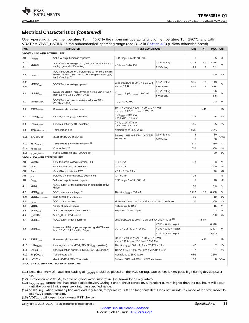
4.5 Electrical CharacteristicsOver operating ambient temperature TA = –40°C to the maximum-operating junction temperature TJ = 150°C, and withVBATP = VBAT_SAFING in the recommended operating range (see R1.2 in Section 4.3) (unless otherwise noted)POS PARAMETER TEST CONDITIONS MIN TYP MAX UNIT
VDD6-BUCK WITH INTERNAL FET
AN CVDD6 Value of output ceramic capacitor (1) ESR range 100 mΩ to 300 mΩ (2) 22 47 µF
AN LVDD6 Value of inductor 22 33 µH
1.1 VDD6 VDD6 output voltage
Average DC value excluding ripple and load transients, VBAT> 7 V, 0 < IVDD6 < 1.3 A, including dc line and load regulation,temperature drift, and long-term drift where VBAT = VBATP =VBAT_SAFING
5.4 6 6.6 V
1.1a VDD6ripple VDD6 ripple voltage Peak-to-peak, ensured by designVBATP = VBAT_SAFING = 14 V, L = 33 µH, C = 22 µF 200 mV
1.2 IVDD6 VDD6 output current IVDD5 + IVDD3/5 + IVDD1+ IVSOUT1(3) 1.3 A
1.3 Vdropout6VDD6 output dropout voltage Vdropout6 = (VBATP –SDN6)
IVDD6 = 1.3 A(example: RDS(on) = 0.46 Ω) 0.6 V
1.4 IVDD6_limit Peak current out of SDN6 pin(4) 1.5 2.5 A
Electrical Characteristics (continued)Over operating ambient temperature TA = –40°C to the maximum-operating junction temperature TJ = 150°C, and withVBATP = VBAT_SAFING in the recommended operating range (see R1.2 in Section 4.3) (unless otherwise noted)POS PARAMETER TEST CONDITIONS MIN TYP MAX UNIT
(11) Less than 50% of maximum loading of IVDD3/5 should be placed on the VDD3/5 regulator before NRES goes high during device powerup.
(12) Protection of VDD3/5, treated as global overtemperature (shutdown for all regulators).(13) IVDD3/5_limit current limit has snap back behavior. During a short circuit condition, a transient current higher than the maximum will occur
until the current limit snaps back into the specified range.(14) VDD1 regulation including line and load regulation, temperature drift and long-term drift. Does not include tolerance of resistor divider to
set VDD1 output voltage.(15) VDD1dyn will depend on external FET choice
VDD3/5 – LDO WITH INTERNAL FET
AN CVDD3/5 Value of output ceramic capacitor ESR range 0 mΩ to 100 mΩ 1 5 µF
3.1aVDD3/5 VDD3/5 output voltage, SEL_VDD3/5 pin: open = 3.3 V
Electrical Characteristics (continued)Over operating ambient temperature TA = –40°C to the maximum-operating junction temperature TJ = 150°C, and withVBATP = VBAT_SAFING in the recommended operating range (see R1.2 in Section 4.3) (unless otherwise noted)POS PARAMETER TEST CONDITIONS MIN TYP MAX UNIT
(16) Referenced to VTRACK1 input, including long-term and temperature drift.(17) VSOUT1 including line and load regulation, temperature drift and long-term drift.(18) VSOUT1 maximum power dissipation for the internal FET must not exceed 0.6 W to avoid overtemperature. Special consideration must
be taken for output voltages greater than 5 V and when VBATP is used to supply VSIN instead of VDD6.(19) VSOUT1 is connected to VSFB1 directly (for unity gain) or through resistor divider (tracking mode gain or non-tracking mode output
voltage adjusting). In case of a short to supply fault, the voltage on VSOUT1 is equal to the supply to the device (VBATP,VBAT_SAFING, and VSIN where VSIN is connected to VBATP as it's supply instead of VDD6) and VSFB1 voltage will follow VSOUT1based on the use case, directly (for unity gain) or via resistor divider (tracking mode gain or non-tracking mode output voltage adjusting).
(20) Protection of VSOUT1 Sensor Supply. Only VSOUT1 switch-offs off.(21) VBATP_UVoff and VBATP_UVon are the threshold levels for VBATP where UV will be indicated by the VBAT_UV bit in VMON_STAT_1
register. The VBATP level that will allow device power up is outlined by R1.1.(22) Brings device into the RESET state and sets flag in SPI(23) Clears flag in SPI
AN CVSOUT1 Value of output ceramic capacitor ESR range 0 mΩ to 100 mΩ 0.5 10 µF
5.1 VSOUT1 VSOUT1 output voltage, depends on external resistivedivider and tracking or non-tracking mode 3.3 9.5 V
5.2 MVVSOUT1
For tracking mode:Matching output error MVVSOUT1 =(VTRACK1 – VSFB1)(16)
0 < IVSOUT1 < 100 mA –35 35 mV
5.3 VSFB1 For non-tracking mode: VSOUT1 reference voltage (17) 10 mA < IVSOUT1 < 100 mA 2.45 2.5 2.55 V
5.3a VTRACK1th
Threshold for selecting tracking/non-tracking mode(VTRACK1 > VTRACK1th_max V for tracking mode,VTRACK1 < VTRACK1th_min V non-tracking mode)
1.1 1.2 1.3 V
5.3b VTRACK1pd Internal pulldown resistance on VTRACK1 pin 100 kΩ
5.4 IVSOUT1VSOUT1 output current, including internal resistor todissipate minimum current (18) 100 mA
5.5 VdrS1 VSOUT1 dropout voltage VdrS1 = (VSIN-VSOUT1) 0 < IVSOUT1 < 100 mA 0.75 V
Electrical Characteristics (continued)Over operating ambient temperature TA = –40°C to the maximum-operating junction temperature TJ = 150°C, and withVBATP = VBAT_SAFING in the recommended operating range (see R1.2 in Section 4.3) (unless otherwise noted)POS PARAMETER TEST CONDITIONS MIN TYP MAX UNIT
(24) Information in SPI register only(25) For device wake up, VBATP and VBAT_SAFING must be operating range, Recommended Operating Conditions R1.1 and R1.3a, and
then a level on either IGN or CANWU to allow the device to start up, especially when VBATP and VBAT_SAFING are ramping.(26) The maximum resistance recommend for RSTEXT to ground is 120 kΩ.
Electrical Characteristics (continued)Over operating ambient temperature TA = –40°C to the maximum-operating junction temperature TJ = 150°C, and withVBATP = VBAT_SAFING in the recommended operating range (see R1.2 in Section 4.3) (unless otherwise noted)POS PARAMETER TEST CONDITIONS MIN TYP MAX UNIT
(27) SEL_VDD3/5 is sampled and latched at device power up hysteresis, VDIGIN_HYST , does not apply.(28) For pins SDO and DIAG_OUT in DMUX mode.
9.5 VENDRV_NRES_TH ENDRV and NRES input readback logic 1 threshold Read-back muxed to DIAG_OUT pin 350 400 450 mV
DIGITAL INPUT / OUTPUT
10.1 VDIGIN_HIGHDigital input, high level for NCS, SDI, SCLK,ERROR/WDI and SEL_VDD3/5 2 V
10.2 VDIGIN_LOWDigital input, low level for NCS, SDI, SCLK,ERROR/WDI and SEL_VDD3/5 0.8 V
10.3 VDIGIN_HYSTDigital input hysteresis for NCS, SCI, SCLK andERROR/WDI (27) 0.1 V
10.4 RDIAGOUT_AMUX Output resistance at DIAG_OUT pin in AMUX mode BG1 selected on AMUX, < 200 nA current in or out ofDIAG_OUT pin 15 kΩ
10.5 VDIGOUT_HIGH Digital output, high level (28) IOUT = –2 mA (out of pin) VDDIO –0.2 V
10.6 VDIGOUT_LOW Digital output, low level(28) IOUT = 2 mA (into pin) 0.2 V
13.13 RPULL_DOWN Internal pulldown resistor on SDI and SCLK input pins 40 70 100 kΩ
(1) 240 µs for VBAT-UV deglitch and 260 µs for VBAT-OV deglitch(2) The system clock is also used to derive the clock for the watchdog timer, so the system clock tolerance also impacts the watchdog-timer
tolerance.(3) Capacitance at CSDO = 100 pF(4) MAX SPI Clock tolerance is ±10%
4.6 Timing RequirementsOver operating ambient temperature TA = –40°C to the maximum-operating junction temperature TJ = 150°C, and VBATP =VBAT_SAFING in the recommended operating range (see R1.2 in the Section 4.3) (unless otherwise noted)POS MIN NOM MAX UNIT
VDD5 – LDO WITH INTERNAL FET
2.12 tdelayVDD5 VDD5 voltage stabilization delayMaximum delay between rising edge onCANWU pin until VDD5 reaches the end-valuewithin 2%
5 ms
VDD3/5 – LDO WITH INTERNAL FET
3.12 tVDD3/5 VDD3/5 voltage stabilization delay Maximum delay after CANWU wakeup forVDD3/5 output to settle 5 ms
VDD1 – LDO WITH EXTERNAL FET
4.15 tdelayVDD1 VDD1 voltage stabilization delay Maximum delay after CANWU wakeup forVDD1 output to settle 5 ms
Timing Requirements (continued)Over operating ambient temperature TA = –40°C to the maximum-operating junction temperature TJ = 150°C, and VBATP =VBAT_SAFING in the recommended operating range (see R1.2 in the Section 4.3) (unless otherwise noted)POS MIN NOM MAX UNIT
13.2 tSPI SPI clock periodVDDIO = 3.3 V 200
nsVDDIO = 5 V 167
13.3 thigh High time: SCLK logic high duration
See Figure 4-2
85.7 ns
13.4 tlow Low time: SCLK logic low duration 45 ns
13.5 tsucsSetup time NCS: time between falling edge of NCS andrising edge of SCLK 45 ns
13.7 tsusiSetup time at SDI: setup time of SDI before the fallingedge of SCLK 15 ns
13.9 thcsHold time: time between the falling edge of SCLK andrising edge of NCS 45 ns
13.10 thlcsSPI transfer inactive time (time between two transfers)during which NCS must remain high 788 ns
(1) Capacitance at CSDO = 100 pF
4.7 Switching CharacteristicsOver operating ambient temperature TA = –40°C to the maximum-operating junction temperature TJ = 150°C, and VBATP =VBAT_SAFING in the recommended operating range (see R1.2 in Section 4.3) (unless otherwise noted)POS PARAMETER TEST CONDITIONS MIN TYP MAX UNITSerial Peripheral Interface Timing (1)
13.6 td1Delay time: time delay from falling edge of NCS to SDOtransitioning from tri-state to 0
See Figure 4-2
53.3 ns
13.8 td2Delay time: time delay from rising edge of SCLK to data validat SDO 0 85.7 ns
13.11 ttriTri-state delay time: time between rising edge of NCS andSDO in tri-state 53.3 ns
5.1 OverviewThe device integrates an asynchronous-buck switch mode power-supply converter with an internal FETthat converts the input battery voltage to a 6-V preregulator output, which supplies the integratedregulators.
A fixed 5-V linear regulator with an internal FET is integrated to be used as, for example, a CAN supply. Asecond linear regulator, also with an internal FET, regulates the 6 V to a selectable 5-V or 3.3-V MCU I/Ovoltage. A linear regulator controller with an external FET and resistor-divider regulates the 6 V to anexternally adjustable core voltage of between 0.8 V and 3.3 V. A linear regulator with two different modesof operation (tracking mode and non-tracking mode) with adjustable voltage between 3.3 V and 9.5 V canbe used as a supply for external sensor.
The device monitors undervoltage and overvoltage on all regulator outputs, battery voltage, and internalsupply rails. A second band-gap reference, independent from the main band-gap reference used forregulation circuit, is used for undervoltage and overvoltage monitoring. In addition, regulator current-limitsand temperature protections are implemented.
The device supports wakeup from IGNITION or wakeup from a CAN transceiver.
5.3.1 VDD6 Buck Switch-Mode Power SupplyThe purpose of the VDD6 buck switch-mode power supply is to reduce the power dissipation inside thedevice as a preregulator. The VDD6 supply regulates from the battery voltage (main supply) range to 6 V.The VDD6 output is used as the input voltage for the VDD5, VDD3/5, VDD1, and can also be used forVSOUT1 regulator depending on the required VSOUT1 output voltage. The VDD6 supply is intended as apreregulator, therefore the output accuracy of VDD6 is less than the other integrated regulators. TheVDD6 current capability is set to supply the VDD5, VDD3/5, VDD1, and VSOUT1 regulators at theirrespective maximum output currents. Power dissipation and thermal analysis should be performed toensure the PCB design and thermal management can support the required power dissipation in theapplication.
This switch-mode power supply operates with fixed-frequency adaptive on-time control PWM. The controlloop is based on a hysteretic comparator. The internal N-channel MOSFET is turned on at the beginningof each cycle if the sensed voltage on the VDD6 pin is below the hysteretic comparator threshold. Whenthe MOSFET is turned on, it is on for a minimum of 7% duty cycle (7% of fclk_VDD6). This MOSFET isturned off when the hysteretic comparator detects a voltage on the VDD6 pin above the threshold. TheVDD6 regulator may skip pulses if the output voltage remains above the hysteretic comparator when theclock edge occurs. When the MOSFET is turned off, the external Schottky diode recirculates the energystored in the inductor for the remainder of the switching period. The VDD6 regulator enters dropout mode(100% duty cycle) for a supply voltage below approximately 7 V on the VBATP pin.
The internal MOSFET is protected from excessive power dissipation by a current-limit circuit. The VDD6regulator also shares an overtemperature protection circuit with the VDD3/5 regulator. Whenovertemperature is detected by this circuit, the device transitions to the STANDBY state (all regulatorsswitched off).
Because the control loop of the VDD6 regulator is based on a hysteretic comparator, the effectivecapacitance on the output, and effective series resistance (ESR) of the output capacitance must beconsidered. The effective capacitance of the output capacitors at the operating voltage (6 V, DC biasderating), tolerance, temperature range, and lifetime must meet the effective capacitance range for VDD6(CVDD6). The capacitor supplier should provide the necessary derating data to calculate the effectivecapacitance. The hysteretic comparator also requires a specified ESR to ensure balanced operation.Typically low-ESR ceramic capacitors are used for the output, so an external resistor is required to bringthe total ESR into the specified ESR range for the CVDD6. A general guideline to achieve balancedoperation is RESR = L / (15 × CEffective). Using a higher-effective output capacitance allows for a lower ESR,which leads to lower-voltage ripple. Additionally, the inductance influences the system: using a lowerinductance value allows for lower ESR, however, the peak inductor current will be higher.
5.3.2 VDD5 Linear RegulatorThe VDD5 pin is a regulated supply of 5 V ±2% overtemperature and battery supply range. A low-ESRceramic capacitor is required for loop stabilization. This capacitor must be placed close to the pin of thedevice. This output is protected against shorts to ground by a current-limit. This output also limits output-voltage overshoot during power up and during line or load transients.
On an initial IGN or CANWU power cycle, the soft-start circuit on this regulator is initiated, which istypically from 1 ms to 2 ms. This output can require a larger output capacitor to ensure that during loadtransients the output does not drop below the required regulation specifications.
The internal MOSFET is protected from excess power dissipation with junction-overtemperatureprotection. In case of an overtemperature condition in the VDD5 pin, only the VDD5 regulator switches offby clearing bit D4 in the SENS_CTRL register. To re-enable the VDD5 pin, bit D4 in the SENS_CTRLregister must be set again.
5.3.3 VDD3/5 Linear RegulatorThe VDD3/5 pin is a regulated supply of 3.3 V or 5 V ±2% overtemperature and battery supply range. Theoutput voltage level is selected with the SEL_VDD3/5 pin (open pin selects 3.3 V, grounded pin selects5 V). The state of this selection pin is sampled and latched directly at the first initial IGN or CANWU powercycle. When latched, any change in the state of this selection pin after the first initial IGN or CANWUpower cycle does not change the initially selected state of the VDD3/5 regulator.
A low-ESR ceramic capacitor is required for loop stabilization. This capacitor must be placed close to thepin of the device. This output is protected against shorts to ground by a current-limit. This output alsolimits output-voltage overshoot during power up or during line or load transients.
On an initial IGN or CANWU power cycle, the soft-start circuit on this regulator is initiated, which istypically from 1 ms to 2 ms. This output may require a larger output capacitor to ensure that during loadtransients the output does NOT drop below the required regulation specifications.
The internal MOSFET is protected from excess power dissipation with a current-limit circuit and junctionovertemperature protection. In case of an overtemperature in the VDD3/5 pin, the TPS65381A-Q1 deviceenters the STANDBY state (all regulators switched-off).
5.3.4 VDD1 Linear RegulatorThe VDD1 pin is an adjustable regulated supply from 0.8 V to 3.3 V. This regulator uses a ±2% reference(VDD1SENSE). The tolerance of the external feedback resistor divider resistors have an impact to theoverall VDD1 regulation tolerance. To reduce on-chip power consumption, an external power NMOS isused. The regulation loop and the command gate drive are integrated. TI recommends applying a resistorwith a value of 100 kΩ to 1 MΩ between the gate and source of the external power NMOS. The VDD1gate output is limited to prevent gate-source overvoltage stress during power up or during line or loadtransients.
On an initial IGN or CANWU power cycle, the soft-start circuit on this regulator is initiated, which istypically from 1 ms to 2 ms. This soft-start is meant to prevent any voltage overshoot at start-up. TheVDD1 output may require larger output capacitor to ensure that during load transients the output does notdrop below the required regulation specifications.
The VDD1 LDO has no current-limit and no overtemperature protection for the external NMOS FET.Therefore, supplying the VDD1 pin from the VDD6 pin is recommended (see Section 5.2). In this way, theVDD6 pin current-limit acts as current-limit for the VDD1 pin and the power dissipation is limited also. Toavoid damage in the external NMOS FET, selecting the current rating of the VDD1 pin well above themaximum-specified VDD6 current-limit is recommended.
If the VDD1 regulator is not used, leave the VDD1_G and VDD1_SENSE pins open. An internal pullupdevice on the VDD1_SENSE pin detects the open connection and pulls up the VDD1_SENSE pin. Thisforces the regulation loop to bring the VDD1_G output down. This mechanism also masks the VDD1_OVflag in VMON_STAT_2 register and therefore the ENDRV pin action from a VDD1 overvoltage (OV)condition is also masked. These actions are equivalent to clearing the NMASK_VDD1_UV_OV bit in theDEV_CFG1 register to 0. This internal pullup device on the VDD1_SENSE pin also prevents a real VDD1overvoltage on the MCU core supply in case of an open connection to the VDD1_SENSE pin, as it bringsthe VDD1_G pin down. Therefore, in this situation, the VDD1 output voltage is 0 V.
By default, VDD1 monitoring is disabled. If the VDD1 pin is used in the application, TI recommends to setthe NMASK_VDD1_UV_OV bit in the DEV_CFG1 register to 1 when the device is in the DIAGNOSTICstate. This setting enables driving and extending the reset to the external MCU when a VDD1undervoltage event is detected.
5.3.5 VSOUT1 Linear RegulatorThe VSOUT1 regulator is a regulated supply with two separate modes: tracking mode and non-trackingmode. The mode selection occurs with the VTRACK1 pin. When the voltage applied on the VTRACK1 pinis above 1.2 V, the VSOUT1 pin is in tracking mode. When the VTRACK1 pin is shorted to ground, theVSOUT1 regulator is in non-tracking mode. This mode selection occurs during the first ramp-up of theVDDx rails and is latched after the first VDDx ramp-up is complete. Therefore, after completion of theVDDx ramp-up, any change on the VTRACK1 pin no longer affects the selected tracking or non-trackingmode.
In tracking mode, the VSOUT1 regulator tracks the input reference voltage on the VTRACK1 pin with again factor determined by the external resistive divider. The tracking offset between the VTRACK1 andVSFB1 pins is ±35 mV. This mode allows, for instance, the VSOUT1 output voltage to be 5 V whiletracking the VDD3 (3.3-V) supply. In unity-gain feedback, the VSOUT1 output voltage can directly followthe VDD5 pin or the VDD3 pin.
In non-tracking mode, the VSOUT1 output voltage is proportional to a fixed reference voltage of 2.5 V atthe VSFB1 pin, with a gain factor determined by the external resistive divider. This mode allows theVSOUT1 pin to be any factor of the internal reference voltage.
Both in tracking and non-tracking mode, the VSOUT1 output voltage must be 3.3 V or higher. TheVSOUT1 regulator can track the VDD3/5 pin in 3.3-V setting within the specified limits.
The VSOUT1 regulator has a separate input supply to reduce the internal power dissipation. For an outputvoltage of 3.3 V or 5 V, for instance, the VDD6 supply can be used as the input supply. For an outputvoltage greater than 5 V, the VBATP pin can be used as the input supply. The maximum powerdissipation for the internal FET must not exceed 0.6 W to avoid overtemperature (thermal shutdown).
A low-ESR ceramic capacitor is required for loop stabilization; this capacitor must be placed close to thepin of the device. This supply limits output-voltage overshoot during power up or during line or loadtransients.
This supply rail is intended for going outside the ECU and therefore is protected against shorts to externalchassis ground by a current-limit. The supply rail can be shorted externally within the specified short circuitvoltages, VSOUT1SH. If the output can be shorted to voltages outside the specified short circuit voltagerange, additional external protection is required.
The VSOUT1 regulator is disabled by default on start-up. After the NRES pin release, the MCU canenable the VSOUT1 regulator through a SPI command by setting bit D0 in the SENS_CTRL register. Afterthis SPI command, the soft-start circuit on this regulator is initiated, which is typically from 1 ms to 2 ms.This output may require a larger output capacitor to ensure that during load transients the output doesNOT drop below the required regulation specifications. Regardless of tracking or non-tracking mode, theVSFB1 pin is ramped to the desired value after completion of the soft start.
The internal MOSFET is protected from excess power dissipation with a current-limit circuit and junction-overtemperature protection. In case of an overtemperature condition in the VSOUT1 pin, only theVSOUT1 regulator is switched off by clearing bit 0 in the SENS_CTRL register. To re-enable the VSOUT1pin, first bit 2 in the SAFETY_STAT 1 register must be cleared on read-out, and afterwards bit 0 in theSENS_CTRL register must be set again.
The VSOUT1 pin voltage can be observed by the ADC input of the MCU through the DIAG_OUT pin (seeSection 5.4.9), which allows the detection of a short to any other supply prior to enabling the VSOUT1LDO.
NOTEThe VSOUT1_EN bit is in the SENS_CTRL register which is only reinitialized by a power-onreset (NPOR) event and not a transition through the RESET state. If the VSOUT1_EN bitwas previously set to 1, it remains set to 1 and the VSOUT1 regulator remains enabled afterevents that cause a transition to the RESET state. In a fault case that would cause anundervoltage or overvoltage on the VSOUT1 pin, when a BIST runs automatically on thetransition from the RESET to the DIAGNOSTIC state, the VSOUT1_UV or VSOUT1_OVcondition during the BIST run would cause the device to go to the SAFE state because of thedetected ABIST_ERR.
5.3.6 Charge PumpThe charge pump is used to generate an overdrive voltage from the VBATP supply that is used for drivingthe gates of the internal NMOS FETs in the VDDx and VSOUT1 supply rails. The charge pump is ahysteretic architecture, when the VCP voltage is high enough, the CP_OV bit sets and the charge pumpstops pumping until the VCP voltage drops below the threshold, the CP_OV bit clears and the chargepump starts pumping again. The charge pump overdrive is provided internally to the device through thelinear regulators, VCP12 and VCP17. Furthermore, this overdrive voltage can drive the gate of an externalNMOS FET acting as reverse-battery protection. Such reverse-battery protection allows for lower batteryvoltage operation compared to a traditional reverse battery-blocking diode. When using the charge pump(VCP) to drive the gate of an NMOS for reverse battery protection, a series resistance of about 10 kΩmust be connected between the VCP pin and the gate of the NMOS FET (see Section 5.2). This seriesresistance is required to limit any current out of the VCP pin when the gate of the NMOS FET is driven toa negative voltage, because the absolute maximum rating of the VCP pin is limited to –0.3 V because of aparasitic reverse diode to the substrate (ground).
The charge pump requires two external capacitors, one pumping capacitor (Cpump) and one storagecapacitor (Cstore). To have sufficient overdrive voltage out of the charge pump even at low battery voltage,the external load current on the VCP pin must be less than 100 µA.
5.3.7 Wake-UpThe TPS65381A-Q1 device has two wake-up pins: IGN and CANWU. Both pins have a wake-up thresholdlevel from 2 V to 3 V, and a hysteresis from 50 mV to 200 mV.
The IGN wake-up pin is level-sensitive and is deglitched with the IGN_deg deglitch (filter) time. TheTPS65381A-Q1 device provides a power-latch function (POST_RUN) for this IGN pin, allowing the MCUto decide when to power down the TPS65381A-Q1 device through SPI command. For this, the MCU mustset the IGN power-latch bit 4 (IGN_PWRL) in the SPI SAFETY_FUNC_CFG register, and read theunlatched status of the deglitched (filtered) IGN pin on the SPI register, DEV_STAT, bit 0 (IGN). To enterthe STANDBY state, the MCU must clear the IGN_PWRL bit. For this, the TPS65381A-Q1 device must bein the DIAGNOSTIC state because this SPI register is only writable in the DIAGNOSTIC state. TheIGN_PWRL bit is also cleared after a detected CANWU wake-up event. Furthermore, the TPS65381A-Q1device provides an optional transition to the RESET state after a detected IGN wake-up duringPOST_RUN (see Figure 5-2).
The CANWU pin is level sensitive and is deglitched with CANWU_deg (filter) time. The deglitched (filtered)CANWU wake-up signal is latched, into CANWU_L, allowing the MCU to decide when to power down theTPS65381A-Q1 device through the WR_CAN_STBY SPI command.
NOTEThe WR_CAN_STBY command should not be written to the device while the CANWU pin orIGN pin is still high. The device starts to transition to the STANDBY state and immediatelytransitions to the RESET state because of the wake-up request received on the CANWU orIGN pin. The registers are reinitialization according to post LBIST (because of a RESETtransition) or according to NPOR (because of a STANDBY transition).
Both the IGN and CANWU pins are high voltage pins. If the pins are connected to lines with transients, theapplication should provide proper filtering and protection to ensure the pins stay within the specifiedvoltage range.
NOTEIf the application does not require wake up from IGN (ignition or KL15) or wake up fromCANWU (a CAN or other transceiver), but the device should wake up any time power issupplied, one method is to connect the IGN pin to the VBATP pin (and VBAT_SAFING)through a 10-kΩ or greater series resistor. When the VBATP supply is turned on, the IGN pinalso goes high and allows the device to wake up (power up) as soon as the voltage levelsallow the release of NPOR circuits for the VBATP and VBAT_SAFING pins, and the IGN pinis high.
5.3.8 Reset ExtensionDuring a power-up event, the TPS65381A-Q1 device releases the reset to the external MCU through theNRES pin with a certain delay time (reset extension time) after the VDD3/5 and VDD1 pins have crossedthe respective undervoltage thresholds.
This reset extension time is externally configurable with a resistor between the RESEXT pin and ground.When shorting the RESEXT pin to ground, the minimum reset extension time is typically 1.4 ms. For a 22-kΩ external resistor, the typical reset extension time is 4.5 ms.
5.4.1 Power-Up and Power-Down BehaviorFigure 5-1 shows the power-up and power-down behavior.
(1) During a power-up event, the analog BIST (ABIST) begins automatically after the VDD6 rail ramps above the UV threshold. If theABIST fails, the device transitions to the SAFE state.
(2) The device may not be able to respond to MCU SPI communication during a BIST, so if the MCU boots faster than the BIST, itshould wait until the BIST is complete to use SPI communication. If the ABIST, LBIST, or both fail, the device transitions to the SAFEstate.
(3) The level of the ENDRV pin depends on the watchdog failure counter, WD_FAIL_CNT[2:0], the ENABLE_DRV bit, and the signalsshown in Figure 5-14. The MCU should only set the ENABLE_DRV bit when the WD_FAIL_CNT[2:0] counter is below 5.
MCU sets IGN_PWRL bitNote: MCU can set this bit only when the device is in DIAGNOSTIC state
IGN going low ignored because IGN_PWRL bit is set
When POST_RUN_RST is set to 1, a re-cranking on IGN pin will put the device in RESET State
DIAGNOSTIC State
Note:Device turns off all internal biasing for low-Iq after internal reference ramp-down time <1 ms. The actual rampdown time of VDD5/3/1 depends on external load conditions
POST_RUN_RST bit cleared when all internal biasing turned-off
IGN_PWRL bit is located in SAFETY_FUNC_CFG SPI registerPOST_RUN_RST bit is located in DEV_CFG2 SPI register
7.5-ms (min) to 22-ms (max) deglitch time
24
TPS65381A-Q1SLVSDJ1A –JULY 2016–REVISED MAY 2017 www.ti.com
(1) Under slow VBAT ramp-down and when the VDD3/5 rail is configured as a 5-V rail, the NRES output can be pulled low when VBATis at approximately 6.3 V. This occurs because of an undervoltage transient on VDD3/5 rail.
(2) Under slow VBAT ramp-up and when the VDD3/5 rail is configured as a 5-V rail, the NRES output can be pulled low when VBAT isat approximately 6.6 V. This occurs because of an undervoltage transient on VDD3/5 rail.
(3) Under similar conditions, undervoltage transients are observed on VDD5 and VSOUT1 rails.
5.4.2 Safety Functions and Diagnostics OverviewThe TPS65381A-Q1 device is intended for use in automotive and industrial safety-relevant applications.The following list of monitoring and protection blocks are those that improve the diagnostic coverage anddecrease the undetected fault rate:• Voltage monitor (VMON)• Analog built-in self-test (ABIST) diagnostics for safety analog blocks• Logic built-in self-test (LBIST) for safety controller functions• Loss-of-clock monitor (LCMON)• Junction temperature monitoring for all power supplies with internal FET• Current-limit for all power supplies• Analog MUX (AMUX) for externally monitored diagnostics and debug• Digital MUX (DMUX) for externally monitored diagnostics and debug• Watchdog configurable for trigger mode (open and close window) or question and answer mode• MCU error signal monitor (ESM) for monitoring the error output from functional safety architecture
MCUs• Controlled and protected enable output (ENDRV) for external power stages or peripheral wakeup• Device configuration register CRC protection• SPI command decoder with parity check• SPI data output feedback check• Reset circuit for initializing external MCU• EEPROM analog trim content CRC protection• Device state controller with SAFE state in case of detected error event
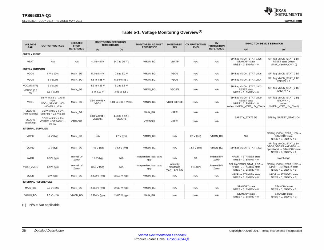
5.4.3 Voltage Monitor (VMON)The VBAT supply voltage, all regulator outputs, and internally generated voltages are supervised by avoltage monitor module (VMON). An undervoltage or overvoltage condition is indicated by thecorresponding VMON register status flag bits:• VMON flag bit cleared to 0 when power supply is within specification• VMON flag bit set to 1 when power supply is outside tolerance band
The monitoring occurs by undervoltage and overvoltage comparators. The reference voltage(BANDGAP_REF2) for the VMON module is independent of the system reference voltage(BANDGAP_REF1) used by the regulators. A glitch-filtering function ensures reliable monitoring withoutfalse setting of the VMON status flag bits. The complete VMON block is supplied by a separate supply pin,VBAT_SAFING.
The VMON comparator diagnostics are covered by the ABIST executed during device startup and powerup or activated with the SPI command by the external MCU SPI request when the device is in theDIAGNOSTIC or ACTIVE state. Each monitored voltage rail is emulated for undervoltage and overvoltageconditions on the corresponding comparator inputs, therefore forcing the corresponding comparator totoggle multiple times (in a toggling pattern observed and checked by the ABIST controller). The monitoredvoltage rails themselves are not affected during this self-test, so no real undervoltage or overvoltage eventoccurs on any of these rails because of this self-test.
Table 5-1 lists an overview of the performed voltage monitoring. As listed in this table, an overvoltageprotection is implemented for some of the internal supply rails.
TPS65381A-Q1www.ti.com SLVSDJ1A –JULY 2016–REVISED MAY 2017
5.4.4 TPS65381A-Q1 Internal Error SignalsTable 5-2 lists a useful overview of the TPS65381A-Q1 device internal error signals and the impact of the signals on the device behavior.
Table 5-2. Internal Error Signals
DETECTIVE CONDITION (THRESHOLD LEVEL) DEGLITCH TIME TO SET FLAG (µs) DEVICE STATE WHEN FLAG IS SET
DMUXPOS. NO. SIGNAL NAME DESCRIPTION MIN TYP MAX UNIT
5.4.5 Loss-of-Clock Monitor (LCMON)The LCMON detects internal oscillator failures including:• Oscillator clock stuck high or stuck low• Reduced clock frequency
The LCMON is enabled during a power-up event after the power-on reset (NPOR) is released. The clockmonitor remains active during device normal operation (STANDBY, RESET, DIAGNOSTIC, ACTIVE, andSAFE states). In case of a clock failure:• The device transitions to the STANDBY state.• All regulators are disabled.• The digital core is reinitialized.• The reset to the external MCU is asserted low.• The failure condition is indicated by the LOCLK bit in the SAFETY_STAT_4 register.
The LCMON has a self-test structure that is activated and monitored by an analog BIST (ABIST). Theexternal MCU can recheck the LCMON any time when the device is in the DIAGNOSTIC state or ACTIVEstate. The enabled diagnostics emulate a clock failure that causes the clock-monitor output to toggle. Theclock-monitor toggling pattern is checked by the ABIST, while the external MCU can check that the loss-of-clock status bit is being set during active test. During this self-test, the actual oscillator frequency (4MHz) is not changed because of this self-test.
5.4.6 Analog Built-In Self-Test (ABIST)The ABIST is the controller and monitor circuit for performing self-checking diagnostics on critical analogfunctions:• VMON undervoltage and overvoltage comparators• Clock monitor (LCMON)• EEPROM analog-trim content check (CRC protection)
During the self-test on the VMON undervoltage and overvoltage comparators, the monitored voltage railsare left unchanged, so no real undervoltage or overvoltage event occurs on any of these rails because ofthese self-tests. Furthermore, also during the self-check on the clock monitor, the actual oscillatorfrequency (4 MHz) is not changed because of this self-test.
(1) For impact to the device state if any ABIST function has a FAIL, see Section 5.4.19.
Figure 5-3. Analog BIST Run States
The ABIST is activated with every device power-up event or any transition to the RESET state. The ABISTcan also be run by the external MCU by setting the ABIST_EN bit in the SAFETY_BIST_CTRL register.During an ABIST run, the device cannot monitor the state of the regulated supplies, and the ENDRV pin ispulled low. The ABIST run time is approximately 300 µs. The ABIST can be performed in the ACTIVEstate on an MCU request, depending on system safety requirements (such as a system-fault responsetime), ENDRV pin will be low during ABIST run.
A running ABIST is indicated in the ABIST_RUN bit (bit D0) in the SAFETY_STAT_3 register. This bit isset to 1 during the ABIST run and is cleared to 0 when the ABIST is complete. In case of an ABIST failurewhile in the DIAGNOSTIC state, including power-up event, the device enters the SAFE state withoutasserting a reset to the external MCU and the ABIST_ERR status flag remains latched in the digital coreuntil a successful ABIST run. This allows the external MCU to detect the ABIST failure by reading theABIST_ERR bits in the SAFETY_STAT_3 register. In case of an ABIST failure while in the ACTIVE state,the device sets the ABIST_ERR status flag, but no state transition occurs.
5.4.7 Logic Built-In Self-Test (LBIST)The logic BIST (LBIST) tests the digital-core safety functions. The LBIST has these characteristics:• An application-controllable logic BIST engine, which applies test vectors to the digital core.• The LBIST engine provides stuck-at fault test coverage to logic blocks under test.• The LBIST run time is typically 4.2 ms (±5%). After the LBIST, a 16-ms (typical) wait period occurs to
fill the digital filters covered by the LBIST. During this time, the ABIST runs. The total BIST time isapproximately 21 ms. The SPI registers may be unavailable during a BIST, so no SPI reads or writesshould be made while the BIST is running.
• The LBIST engine has a time-out counter as a fail-safe feature.
The BIST (LBIST with ABIST) is activated and run in the DIAGNOSTIC state with any transition out of theRESET state during power-up events. The BIST is also activated with any other transition out of theRESET state unless the AUTO_BIST_DIS bit in the SAFETY_BIST_CTRL register is set.
The MCU can run the LBIST (BIST) by setting the LBIST_EN bit in the SAFETY_BIST_CTRL register.
NOTEIn the ACTIVE state the following considerations must be considered if a manual run of theLBIST is initiated by setting the LBIST_EN bit to 1. The LBIST should only be run in theACTIVE state if the system-safety timing requirements can allow the total 21-ms BIST timeand ENDRV being low for the 21-ms time.
NOTEIn the ACTIVE or DIAGNOSTIC or SAFE state the following considerations must beconsidered if a manual run of the LBIST is initiated by setting the LBIST_EN bit to 1. Afterthe LBIST is complete the WD_FAIL_CNT[2:0] counter is re-initialized to 5. The MCU shouldresynchronize to the TPS65381A-Q1 watchdog by writing to the WD_WIN1_CFG orWD_WIN2_CFG register or by immediately causing a bad event. Both of theseresynchronization options start a new watchdog sequence and increment theWD_FAIL_CNT[2:0] counter. If the WD_RST_EN bit is set to 1 (enabled), the watchdogservice routine in the MCU must ensure good events are sent to the watchdog to startdecrementing the WD_FAIL_CNT[2:0] counter before it reaches 7 +1 which cause atransition to the RESET state. After the LBIST is complete some of the registers arereinitialized. If the these configuration registers change from the initialized values, theseregisters must be reconfigured to the required setting for the application.
NOTEIn the DIAGNOSTIC state the following considerations must be taken into account if amanual run of the LBIST is initiated by setting the LBIST_EN bit to 1. Setting the LBIST_ENbit to 1 clears the DIAG_EXIT_MASK bit to 0. If the DIAG_EXIT_MASK bit is being used tohold the device in the DIAGNOSTIC state for software debug, it must be set again to 1 afterLBIST completion to stay in the DIAGNOSTIC state. The DIAGNOSTIC state time-outcounter stops only during the running of the LBIST. After the LBIST is complete, the time-outcounter continues from the last value. For a transition from the DIAGNOSTIC state to theACTIVE state, the DIAG_EXIT bit must be set to 1.
During the BIST run, the device cannot monitor the state of regulated supplies and cannot respond to anySPI command, and therefore cannot monitor the state of the MCU through the watchdog timer. During theBIST run, the ENDRV pin is pulled low and the watchdog fail counter reinitializes to 5. After the BIST iscomplete, the following functions and registers reinitialize:• DEV_STAT• SAFETY_STAT_2• SAFETY_STAT_4• SAFETY_STAT_5 (but FSM[2:0] will immediately update to reflect the current device state)• WD_TOKEN_VALUE• WD_STATUS• SAFETY_CHECK_CTRL• DIAG_CFG_CTRL• DIAG_MUX_SEL
A running LBIST is indicated in the LBIST_RUN bit (bit D1) in the SAFETY_STAT_3 register. This bit isset to 1 while the LBIST is running and is cleared to 0 when the LBIST is complete. After the LBIST run,completion of the whole BIST is confirmed by the MCU by reading 0 for both the LBIST_RUN andABIST_RUN bits.
In case of an LBIST failure in the DIAGNOSTIC state, the device enters the SAFE state. The externalMCU can detect the LBIST failure by reading the LBIST_ERR bit in the SAFETY_STAT_3 register. Incase of an LBIST failure while in the ACTIVE state, the device sets the LBIST_ERR status flag, but nostate transition occurs. Because the ABIST is run during the LBIST, the ABIST_ERR bit can also bemonitored by the MCU.
5.4.8 Junction Temperature Monitoring and Current LimitingEach LDO with an internal power FET has junction temperature monitoring with overtemperatureprotection (thermal shutdown). In case of an overtemperature condition, a regulated supply can re-enableonly after the overtemperature condition is removed.
For the VSOUT1 regulator, the overtemperature condition disables the regulator and clears the enable bit(VSOUT1_EN), while all other regulators remain enabled. When the VSOUT1 overtemperature conditionis gone, the external MCU must set the enable control bit again to re-enable the regulator.
The VDD3/5 and VDD6 regulators share an overtemperature protection circuit. A overtemperature eventdisables the VDD3/5 regulator. If the NMASK_VDD3/5_OT is set to 1 (default), the device transitions tothe STANDBY state. If the NMASK_VDD3/5_OT bit is cleared to 0, the device transitions to the RESETstate when the VDD3/5 output reaches the UV level for the VDD3/5 regulator. In both cases the NRES pingoes low and resets the external MCU and the ENDRV pin is low. TI recommends using the device withthe NMASK_VDD3/5_OT bit set to 1.
For the VDD5 regulator, the overtemperature condition clears the VDD5_EN enable bit and transitions tothe RESET state. NRES pin goes low and resets the MCU and the ENDRV pin is low. All other regulatorsremain enabled. When the VDD5 overtemperature condition is gone, the MCU must set the enable controlbit again to re-enable the regulator.
The VDD6, VDD3/5, VDD5, and VSOUT1 regulators include a current-limit circuit for protection againstexcessive power consumption and thermal overstress.
5.4.9 Diagnostic MUX and Diagnostic Output Pin (DIAG_OUT)Analog and digital critical signals, which are not directly connected to the MCU, are switched by amultiplexer to the external DIAG_OUT pin. The programming of the multiplexer is done with theDIAG_MUX_SEL register. The digital signals are buffered to have sufficient drive capabilities.
This multiplexer facilitates external pin-interconnect tests by feeding back the input pin state or feedingback internal module self-test status or safety comparator outputs.
A. These analog signals are multiplexed out with a divide ratioB. If the application must measure analog signals with an MCU ADC and monitor digital signals with an MCU GPIO, the
application design must assure the GPIO input stage does not affect the ADC measurements. If isolating the MCUGPIO is not possible within the MCU, the application design must achieve the necessary isolation externally.
Figure 5-4. Diagnostic Output Pin, DIAG_OUT
In case the DIAG_OUT pin is connected to a mixed analog or digital input pin of the MCU, TI recommendsconfiguring this MCU input pin and the DIAG_OUT pin simultaneously in accordance with the desired typeof signal (analog or digital). The type of signal (analog or digital) on the DIAG_OUT pin can be configuredwith the MUX_CFG[1:0] bits in the DIAG_CFG_CTRL register. The DIAG_OUT multiplexer can be globallyenabled and disabled with bit 7 in the DIAG_CFG_CTRL register. When disabled, the DIAG_OUT pin is inthe high-ohmic state (tri-state).
NOTEWhen enabling the DIAG_OUT MUX while using SPI communication, the SDO pin is not inthe high impedance state while the NCS pin is high and the DIAG_OUT MUX is enabled.Software or hardware modification may be required in the application. For hardwaremodifications check the SDO threshold level and drive capability if resistors are used toadjust the voltage level of the SDO pin on the SPI bus or use a buffer gate with an enableand tri-state output such as the SN74AHC1G125 to allow the downstream SDO signal to bein the high impedance state if required in the application while the NCS pin is high even if theDIAG_OUT MUX is enabled.
(1) The supply range is the input supply range for VBATP and VBAT_SAFING (VBATP = VBAT_SAFING).(2) The given accuracies are without the DC load-current drawn from the DIAG_OUT pin. For overall accuracy calculation, the divide ratio
accuracy and the drop voltage caused by IDIAG_OUT × output resistance must be considered.
5.4.9.1 Analog MUX (AMUX)
Table 5-4 lists the selectable-analog internal signals on the DIAG_OUT pin. In the DIAG_CFG_CTRLregister, the MUX_CFG[1:0] bits must be set to 10b for the analog MUX mode.
Table 5-4. Analog MUX Selection Table
SIGNALNUMBER
VOLTAGERAIL
orSIGNALNAME
DESCRIPTION SUPPLYRANGE (1)
DIVIDERATIO
DIVIDE RATIOACCURACY (2)
OUTPUT RESISTANCE(kΩ) DIAG_MUX_SEL[7:
0]MINIMUM MAXIMUM MINIMUM MAXIMUM
A.1 VDD5 Linear VDD5regulator output 5.8 to 34 V 2 –2.25 % 0.75 % 20 50 0x01
A.2 VDD6 Switch modepreregulator 5.8 to 34 V 3 –3.75% 0.5 % 30 100 0x02
A.3 VCP Charge pump5.8 to 18V
13.5–6.25 % 2.25 %
90 200 0x045.8 to 34 V –6.25% 4.75 %
A.4 VSOUT1 Sensor supplyvoltage 5.8 to 34 V 4 –0.5 % 1.2 % 40 100 0x08
A.5 VBAT_SAFING
Battery (supply)input for monitoring(VMON) and BG2functions
5.8 to 18 V
10
–5 % 0 %
125 200 0x105.8 to 34 V –5 % 5.5 %
A.6 VBATP Battery (supply),main power supply
5.8 to 18V10
–5 % 0 %125 200 0x20
5.8 to 34 V –5 % 5.5 %
A.7 MAIN_BG Regulators band-gap reference 5.8 to 34 V 1 NA 3 15 0x40
A.8 VMON_BG Voltage-monitorband gap 5.8 to 34 V 1 NA 3 15 0x80
In case one of the AMUX signals after the divide ratio is at a voltage above the VDDIO voltage, a clampbecomes active to avoid any voltage level higher than the VDDIO voltage on the DIAG_OUT pin.
To achieve the fastest stabilization of the signal switched to the DIAG_OUT pin, following the AMUXswitching order from A.1 up to A.8 is not recommended.
The recommendation is to switch the order from high-to-low voltage, starting with A.8. For example: A.8 –A.7 – A.1 – A.2 – A.3 – A.5 – A.6 – A.4.
NOTEThe sensor-supply output voltage (VSOUT1) is 0 V in this example. If the VSOUT1 voltage ishigher, then the switching order described in the previous example must be changed.
NOTEIn the application, a series resistance of at least 100 kΩ is required on the input capacitorfilter of the ADC input of the MCU.
5.4.9.2 Digital MUX (DMUX)
The following tables list the selectable digital internal signals on the DIAG_OUT pin. In theDIAG_CFG_CTRL register, the MUX_CFG[1:0] bits must be cleared to 01b for the digital MUX mode.
Most of these signals are internal error signals that influence the device state and behavior of the NRESpin and the ENDRV pin. See Table 5-2 for a more detailed table listing the internal error signals and theirimpact on the device behavior.
D1.1 RSV Reserved, logic 0 000b 0000bD1.2 NAVDD_UV AVDD undervoltage comparator output (inverted) 000b 0001bD1.3 BG_ERR1 VMON or main band gap is OFF 000b 0010bD1.4 BG_ERR2 VMON or main band gap is OFF 000b 0011b
D5.1 RSV Reserved, logic 0 111b 0000bD5.2 TI_TEST_MODE TI production test mode indication 111b 0001bD5.3-16 DFT Signal reserved for production test 111b 0010b-1111b
A diagnostic check at the SDO digital-output pin is also possible in DMUX mode. For this diagnosticcheck, the following sequence is required:1. The MUX_CFG[1:0] configuration must be set to 01b for DIGITAL MUX mode.2. The SPI NCS must be kept HIGH.3. The state of the SDO pin is controlled by the SPI_SDO bit (bit D6 in the DIAG_CFG_CTRL register).
During this SDO check at the SDO pin, the DIAG_OUT pin is kept low if no signal from the Digital MUXSelection table is selected.
5.4.9.3 Diagnostic MUX Output State (by MUX_OUT bit)
For a diagnostic interconnect check between the DIAG_OUT pin and the MCU analog-digital input pin, thestate of the DIAG_OUT pin is controlled with the SPI bit, MUX_OUT, in the DIAG_CFG_CTRL register. Touse this mode, the MUX_CFG[1:0] bits must be set to 00b in the DIAG_CFG_CTRL register.
5.4.9.4 MUX Interconnect Check
For performing a diagnostic interconnect check at the digital input pins (ERROR/WDI, NCS, SDI, andSCLK), the MUX_CFG[1:0] bits in the DIAG_CFG_CTRL register must be set to 11b. The INT_CON[2:0]bits in the DIAG_CFG_CTRL register can select which of these digital inputs to be multiplexed to theDIAG_OUT pin (see the description of DIAG_CFG_CTRL register in Section 5.5.1).
5.4.10 Watchdog Timer (WD)The watchdog monitors the correct operation of the MCU. This watchdog requires specific triggers, ormessages, from the MCU in specific time intervals to detect correct operation of the MCU. The MCU cancontrol the logic level of the ENDRV pin with the ENABLE_DRV bit when the watchdog detects correctoperation of the MCU. When the watchdog detects incorrect operation of the MCU, the device pulls theENDRV pin low. This ENDRV pin can be used in the application as a control signal to deactivate thepower output stages, for example a motor driver, in case of incorrect operation of the MCU. This functionis consequently referred to as the watchdog-enabled function.
The watchdog has two different modes, which are defined as follows:Trigger mode: In trigger mode, the MCU applies a trigger (pulse) on the ERROR/WDI pin to send the
required watchdog event for trigger mode. The watchdog operates in trigger mode as thedefault mode when the device goes from the RESET state to the DIAGNOSTIC state. TheMCU error signal monitor (ESM) should not be used when the watchdog operates in triggermode.
Question-answer mode (Q&A mode): In Q&A mode, the MCU sends watchdog answers through SPI.
To select the Q&A mode, the MCU must set the WD_CFG bit (bit 5) in the safety-function configurationregister (SAFETY_FUNC_CFG) while in the DIAGNOSTIC state. When the watchdog operates in Q&Amode, the MCU error signal monitor (ESM) may be used.
5.4.11 Watchdog Fail Counter, Status, and Fail EventThe watchdog includes a watchdog fail counter (WD_FAIL_CNT[2:0]) which increments because of badevents or decrements because of good events. When the value of the watchdog fail counter is 5 or more,the watchdog status is out-of-range and the ENDRV pin is low (the watchdog-enabled function isdisabled).
When the watchdog fail counter is 4 or less, the watchdog status is in-range and the watchdog no longerdisables the watchdog-enabled function. In this case, the device pulls up the ENDRV pin when theENABLE_DRV control bit (in the SAFETY_CHECK_CTRL register) is set and when the device detects noother errors that impact the level of the ENDRV pin.
The watchdog fail counter operates independently of the state of the watchdog reset configuration bit (bit3), WD_RST_EN, in the SAFETY_FUNC_CFG register.
The watchdog fail counter responds as follows:• A good event decrements the fail counter by one, down to the minimum of zero.• A bad event increments the fail counter by one, up to the maximum of seven.• A time-out event increases the fail counter by one, up to the maximum of seven, and sets the
TIME_OUT flag (WD_STATUS register, bit 1).
The definitions of good event, bad event and time-out event are listed Section 5.4.14 and Section 5.4.15.
Figure 5-5. Watchdog Impact on ENDRV and RESET
Table 5-10. Watchdog Status for Range of the Watchdog Fail Counter Value
WATCHDOG FAILCOUNTER
WD_FAIL_CNT[2:0]000b THROUGH 100b 101b THROUGH 111b 111b
The watchdog status is basedon the WD_FAIL_CNT[2:0]value.
Watchdog in-range Watchdog is out-of-range
If the WD_RST_ENbit is set to 1, theNRES pin is pulledlow, the device is inthe RESET state onnext "bad" or "time-out" event to thewatchdog
The watchdog fail counter is initialized to a count of 5 when the device enters the DIAGNOSTIC state(after going through the RESET state) and when the device transitions from the DIAGNOSTIC state to theACTIVE state.
When the watchdog fail counter reaches a count of 7, another bad event does not change the counter: thecounter remains at 7. However, if the watchdog reset is enabled (WD_RST_EN bit in theSAFETY_FUNC_CFG register is set to 1), on the next bad event or time-out event (7 + 1) the deviceenters the RESET state and resets the MCU by pulling the NRES pin low. In the RESET state, thewatchdog fail counter reinitializes to 5. If the watchdog fail counter is at seven when the WD_RST_EN bitis set to 1, the device immediately enters the RESET state without requiring another bad event or time-outevent.
5.4.12 Watchdog SequenceEach watchdog sequence begins with a Window 1 followed by a Window 2. The MCU can program thetime periods of Window 1 (tWIN1) and Window 2 (tWIN2) with the WD_WIN1_CFG and WD_WIN2_CFGregisters respectively when the device is in the DIAGNOSTIC state. When the device goes from theRESET state to the DIAGNOSTIC state, the watchdog sequence begins with the default tWIN1 and tWIN2time periods.
Use Equation 1 and Equation 2 to calculate the minimum and maximum values for the tWIN1 time period.Use Equation 3 and Equation 4 to calculate the minimum and maximum values for the tWIN2 time period.
tWIN1_MIN = [(RT[6:0] – 1) × 0.55 × 0.95] ms
where• The bits RT[6:0] are located in the WD_WIN1_CFG SPI register.
(1)tWIN1_MAX = (RT [6:0] × 0.55 × 1.05) ms
where• The bits RT[6:0] are located in the WD_WIN1_CFG SPI register.
(2)tWIN2_MIN = [(RW[4:0] + 1) × 0.55 × 0.95] ms
where• The bits RW[4:0] are located in the WD_WIN2_CFG SPI register.
(3)tWIN2_MAX = [(RW[4:0] + 1) × 0.55 × 1.05] ms
where• The bits RW[4:0] are located in the WD_WIN2_CFG SPI register.
(4)
If the MCU stops sending events, or stops feeding the watchdog during the watchdog sequence, thewatchdog considers this lack of response from the MCU a time-out event (no response event). This setsthe TIME_OUT status bit (bit 1 in the WD_STATUS register) and increments the watchdog fail counter.Immediately following a time-out event the next watchdog sequence is started.
Based on the Window 1 and Window 2 time periods, the watchdog sequence and time-out time periodsare calculated as follows:
The watchdog uses the internal system clock of the device (±5% accuracy) as a time reference forcreating the 0.55-ms watchdog time step. WINDOW 1 may be up to one 0.55-ms watchdog time stepshorter than programmed as indicated by Equation 1.
NOTEBecause of the uncertainty in the Window 1 and Window 2 time periods, TI recommendsusing settings for Window 1 and Window 2 of two or higher. Window 2 could be set as lowas one, assuming Window 1 is set to six or lower. The response from the MCU should betargeted to the mid point of known timing for Window 2. As Window 1 setting is increasedabove six, the device system-clock tolerance (±5%) becomes large compared to a setting ofone in Window 2 not allowing for a known time range for a response in Window 2, soWindow 2 setting must be scaled with Window 1 to allow timing margin.
5.4.13 MCU to Watchdog SynchronizationTo synchronize the MCU with the watchdog sequence, the MCU can write to either the WIN1_CFG orWIN2_CFG registers to start a new watchdog sequence. After a write access to the WIN1_CFG orWIN2_CFG register by the MCU (even when these registers are locked or when the device is in theACTIVE or the SAFE state), the device immediately starts a new watchdog sequence and increments thewatchdog fail counter. Therefore a write access to the WD_WIN1_CFG or WD_WIN2_CFG register onlytakes effect in this new watchdog sequence.
When the MCU is synchronized with the watchdog sequence, a good event from the MCU immediatelystarts a new watchdog sequence. In this way, the MCU stays synchronized with the watchdog sequence.
See Figure 6-11 for an example software flowchart of how to synchronize the MCU with the TPS65381A-Q1 watchdog.
5.4.14 Trigger Mode (Default Mode)When the device goes from the RESET state to the DIAGNOSTIC state, the watchdog operates in triggermode (default). The first watchdog sequence begins with the default tWIN1 and tWIN2 time periods. Thewatchdog receives the triggers from the MCU on the ERROR/WDI pin. A rising edge on the ERROR/WDIpin, followed by a falling edge on the ERROR/WDI pin after more than the required pulse time,tWD_pulse(max) (32 μs), is a trigger. Even a waveform with a longer duration high than low is counted as atrigger if the rising and falling edges meet this requirement.
Window 1, called a CLOSE window, is the first window in the watchdog sequence. A trigger received inWindow 1 is a bad event and ends Window 1, starts a new watchdog sequence and setsANSWER_EARLY flag.
Window 2, called an OPEN window, follows Window 1. At a minimum, Window 2 lasts until a trigger isreceived. At a maximum, Window 2 lasts until the programmed tWIN2 time. A trigger received in Window 2(OPEN) is a good event. A new watchdog sequence begins immediately after the watchdog receives atrigger in Window 2.
If the MCU stops sending triggers during the watchdog sequence, the watchdog considers this lack ofresponse from the MCU a time-out event (no response event). This sets the TIME_OUT status bit (bit 1 inthe WD_STATUS register) and increments the watchdog fail counter. Immediately following a time-outevent a new watchdog sequence is started.
The TIME_OUT flag can be useful for the MCU software to resynchronize the watchdog trigger pulseevents to the required device watchdog timing. When resynchronizing in this way, the MCU detects theTIME_OUT flag being set. The TIME_OUT flag being set indicates the time-out event and the start of anew watchdog sequence. The MCU should send the trigger with timing so the trigger is in Window 2(OPEN) of this new watchdog sequence.
NOTEIf an active SPI frame (nCS is low) is present when the time-out event occurs, theTIME_OUT flag is not latched (set) in the WD_STATUS register, but the watchdog failcounter still increments. Because the TIME_OUT flag is not latched, this impacts theresynchronization ability of the MCU and status monitoring. It is recommended to use thesynchronization procedure outlined in section Section 5.4.13.
In trigger mode, the watchdog uses a deglitch filter with the tWD_pulse filter time and an internal systemclock to create the internally generated watchdog pulse (see Figure 5-6 and Figure 5-7).
The rising edge of the trigger on the ERROR/WDI pin must occur at least the tWD_pulse(max) time before theend of Window 2 (OPEN) to generate a good event.
The window duration times of Window 1 (CLOSE) and Window 2 (OPEN) are programmed through theWD_WIN1_CFG and WD_WIN2_CFG registers when the device is in the DIAGNOSTIC state. In triggermode, the window duration time are as follows:
tWCW_MIN (Trigger mode) = tWIN1_MIN
where• WCW is a watchdog CLOSE window
(7)tWCW_MAX (Trigger mode) = tWIN1_MAX
where• WCW is a watchdog CLOSE window
(8)tWOW_MIN (Trigger mode) = tWIN2_MIN
where• WOW is a watchdog OPEN window
(9)tWOW_MIN (Trigger mode) = tWIN2_MIN
where• WOW is a watchdog OPEN window
(10)
Use Equation 1 and Equation 2 to calculate the minimum and maximum values for the tWIN1 = tWCW timeperiod. Use Equation 3 and Equation 4 to calculate the minimum and maximum values for the tWIN2 = tWOWtime period.
Writing a new Window 1 or Window 2 time to the WD_WIN1_CFG or WD_WIN2_CFG registerimmediately begins a new watchdog sequence and increments the watchdog fail counter. A new watchdogsequence is started by a write even when WD_WIN1_CFG register and the WD_WIN2_CFG SPI registerare locked because the device is not in DIAGOSTIC state or the SPI command SW_LOCK is blocking awrite update to the register values.
The watchdog trigger event is considered a good-event if received during a Window 2 (OPEN) window,and is considered a bad-event if received during Window 1 (CLOSE) window. A good-event ends thecurrent watchdog sequence and starts a new watchdog sequence, therefore the MCU and devicewatchdog timing stay synchronized.
A good-event, bad-event, time-out event, power-up event, or power-down event ends the currentwatchdog sequence and starts a new watchdog sequence.
Note: The deglitch time of the WD trigger on ERROR/WDI is tWD_pulse. tWD_pulse (min) = 28 µs and tWD_pulse (max) = 32 µs The rising edge of the external trigger signal must be no later than 32 µs before WINDOW 2 ends to ensure the deglitched signal occurs within WINDOW 2.
Note: The external trigger signal may start in WINDOW 1, as long as the rising edge of the internally generated watchdog pulse (derived from the deglitched trigger on ERROR/WDI pin) is in WINDOW 2.
A A
Decrement WD_FAIL_CNT[2:0]WD_FAIL_CNT[2:0]=4
BIST Run Time
WD_FAIL_CNT[2:0]=5
Decrement WD_FAIL_CNT[2:0]WD_FAIL_CNT[2:0]=3
t > tWD_pulse
tWD_pulsetWD_pulse
tWD_pulse tWD_pulse
Start New Watchdog Sequence Start New Watchdog Sequence
TPS65381A-Q1www.ti.com SLVSDJ1A –JULY 2016–REVISED MAY 2017
A. When a good event is received in Window 2, 1 system clock-cycle (250 ns, typical) later the next watchdog sequence begins. Therefore the actual length of Window 2depends on when the MCU sends the good event.
Figure 5-6. Example Cases for Good-Events in Trigger Mode
WD_FAIL_CNT[2:0] remains at 7 while WD_RST_EN = 0B
WD_FAIL_CNT[2:0]=7
Start New Watchdog Sequence
NRES = HIGH When WD_FAIL_CNT[2:0] = 7 + 1
AND WD_RST_EN = 0B
WINDOW 1 (CLOSE)
t > tWD_pulse
C A A
A
Note: The deglitch time of the WD trigger on ERROR/WDI is tWD_pulse. tWD_pulse (min) = 28 µs and tWD_pulse (max) = 32 µs Any external trigger signal that his high longer than 32 µs will be deglitched and propagate into the watchdog as the Internally Generated Watchdog Pulse.
TPS65381A-Q1SLVSDJ1A –JULY 2016–REVISED MAY 2017 www.ti.com
A. When a time-out event occurs, 1 system clock-cycle (250 ns, typical) later, the next watchdog sequence begins.B. WD_RST_EN = 0 per default. To enable a reset from the watchdog once WD_FAIL_CNT[2:0] = 7 +1, WD_RST_EN must be set to 1. The notation WD_FAIL_CNT[2:0]
= 7 +1 means the next (+ 1) bad event or time-out event if WD_FAIL_CNT[2:0] = 7 while WD_RST_EN = 1 will cause a transition to the RESET state. However, whenWD_RST_EN = 0, the WD_FAIL_CNT[2:0] counter does not increment past 7 and the watchdog does not cause a transition to the RESET state.
C. When a bad event is received in Window 1, 1 system clock-cycle (250 ns, typical) later the next watchdog sequence begins. Therefore the actual length of Window 1depends on when the MCU sends the bad event.
Figure 5-7. Example Cases for Bad-Event and Time-out Events in Trigger Mode
5.4.15 Q&A ModeSetting the WD_CFG bit in the SAFETY_FUNC_REG register to 1 when the device is in the DIAGNOSTICstate configures the watchdog for Q&A (question and answer) mode. In Q&A mode, the device provides aquestion (or TOKEN) for the MCU in the WD_TOKEN_VALUE register. The MCU performs a fixed seriesof arithmetic operations on the question to calculate the required 32-bit answer. This answer is split intofour answer bytes or responses. The MCU writes these answer bytes through SPI one byte at a time intothe WD_ANSWER register. The device verifies that the MCU returned the answer bytes within thespecified timing windows, and that the answer bytes are correct.
A good event occurs when the MCU sends the correct answer bytes calculated for the current questionwithin the correct watchdog window and in the correct order.
A bad event occurs when one of the events that follows occur:• The MCU sends the correct answer bytes, but not in the correct watchdog window.• The MCU sends incorrectly calculated answer bytes.• The MCU returns correct answer bytes in the wrong order (sequence).
If the MCU stops sending answer bytes during the watchdog sequence, the watchdog considers this lackof response from the MCU a time-out event (no response event). This sets the TIME_OUT status bit (bit 1in the WD_STATUS register) and increments the watchdog fail counter. Immediately following a time-outevent a new watchdog sequence is started.
The TIME_OUT flag can be useful for the MCU software to resynchronize the watchdog answer timing tothe required device watchdog timing. When resynchronizing in this way, the MCU detects the TIME_OUTflag being set. The TIME_OUT flag being set indicates the time-out event and the start of a new watchdogsequence. The MCU should send the answer bytes with timing so they will be in the correct windows ofthe new watchdog sequence.
NOTEIf an active SPI frame (nCS is low) is present when the time-out event occurs, theTIME_OUT flag is not latched (set) in the WD_STATUS register, but the watchdog failcounter is still incremented. Because the TIME_OUT flag is not latched this impacts theresynchronization ability of the MCU and status monitoring. It is recommended to use thesynchronization procedure outlined in section Section 5.4.13.
NOTEIn Q&A mode, each watchdog sequence starts with Window 1 (OPEN) followed by Window 2(CLOSE). The OPEN and CLOSE references for Q&A mode are reversed with respect tothose of trigger mode, but the order of the Window 1 and Window 2 is the same as are theregisters containing the setting for each window, WD_WIN1_CFG and WD_WIN2_CFG.
5.4.15.1 Watchdog Q&A Related Definitions
The Q&A mode definitions are:Question (Token) The question (token) is a 4-bit word (see Section 5.4.15.3).
The watchdog provides the question (token) to the MCU when the MCU reads the question(TOKEN[3:0]) from the WD_TOKEN_VALUE register.The MCU can request each new question (token) at the start of the watchdog sequence, butthis is not required to calculate the answer. The MCU can also generate the question byimplementing the question generation circuit as shown in Figure 5-9. Nevertheless, theanswer and, therefore the answer bytes, are always based on the question generated insidethe watchdog of the device. So, if the MCU generates a wrong question and gives answerbytes calculated from a wrong question, the watchdog detects a bad event.A new question (token) is generated only when a good event occurred in the previouswatchdog sequence causing the token counter (internal counter) to increment and generate
a new question (token) as shown in figure Figure 5-9.Answer (Response) The answer (response) is a 32-bit word that is split into four answer bytes or
responses: Answer-3 (WD_TOKEN_RESP_3), Answer-2 (WD_TOKEN_RESP_2), Answer-1(WD_TOKEN_RESP_1), and Answer-0 (WD_TOKEN_RESP_0).The watchdog receives an answer byte when the MCU writes to the watchdog answerregister (the WD_ANSW[7:0] bits in the WD_ANSWER register).For each question, the watchdog requires four correct answer bytes from the MCU in thecorrect timing and order (sequence). Answer-3, Answer-2, and Answer-1 can be in Window1 or Window 2 in the correct order, and Answer-0 must be in Window 2 to be detected as agood event.
5.4.15.2 Watchdog Sequence in Q&A Mode
The watchdog sequence in Q&A mode ends after the MCU writes the fourth answer byte, Answer-0(WD_TOKEN_RESP_0), or after a time-out event. A new watchdog sequence starts after the previouswatchdog sequence ends.
The window duration times of Window 1 (OPEN) and Window 2 (CLOSE) are programmed through theWD_WIN1_CFG and WD_WIN2_CFG registers when the device is in the DIAGNOSTIC state. In Q&Amode, the window duration time are as follows:
tWOW_MIN (Q&A mode) = tWIN1_MIN
where• WOW is a watchdog OPEN window
(11)tWOW_MAX (Q&A mode) = tWIN1_MAX
where• WOW is a watchdog OPEN window
(12)tWCW_MIN (Q&A mode) = tWIN2_MIN
where• WCW is a watchdog CLOSE window
(13)tWCW_MIN (Q&A mode) = tWIN2_MIN
where• WCW is a watchdog CLOSE window
(14)
Use Equation 1 and Equation 2 to calculate the minimum and maximum values for the tWIN1 = tWOW timeperiod. Use Equation 3 and Equation 4 to calculate the minimum and maximum values for the tWIN2 = tWCWtime period.
Writing a new Window 1 or Window 2 time to the WD_WIN1_CFG or WD_WIN2_CFG registerimmediately begins a new watchdog sequence and increments the watchdog fail counter. A new watchdogsequence is started by a write even when WD_WIN1_CFG register and the WD_WIN2_CFG SPI registerare locked because the device is not in DIAGOSTIC state or the SPI command SW_LOCK is blocking awrite update to the register values.
The first three correct answer bytes (responses) may be scheduled in WINDOW 1 or WINDOW 2. The first three answer bytes must be in the correct order (sequence):
x� Answer-3 (WD_TOKEN_RESP_3) followed byx� Answer-2 (WD_TOKEN_RESP_2) followed byx� Answer-1 (WD_TOKEN_RESP_1)
After WINDOW 1 time elapses, WINDOW 2 begins.
The MCU needs to write the answer bytes (responses) to WD_ANSWER register.
The fourth answer byte, Answer-0 (WD_TOKEN_RESP_0) must be provided in WINDOW 2.
After the MCU writes the fourth answer byte (Answer-0) to the WD_ANSWER register, the watchdog generates the next question (token) after which next watchdog sequence begins.
MCU Provides Answer(2)
AnswerQuestion
MCU Reads Question(1)
SPI Commands
NCS pin
1 Internal Clock Cycle (250 ns)to Generate New Question for (Q&A [n + 1])
Q&A [n] Q&A [n + 1]
Q* = RD_WD_TOKEN_VALUE3* = Answer-3 to WR_WD_ANSWER2* = Answer-2 to WR_WD_ANSWER1* = Answer-2 to WR_WD_ANSWER0* = Answer-0 to WR_WD_ANSWER
Q* 3* 2* 1* 0*
47
TPS65381A-Q1www.ti.com SLVSDJ1A –JULY 2016–REVISED MAY 2017
(1) The MCU is not required to read the question (token). The MCU can begin giving the correct answer bytes Answer-3, Answer-2,Answer-1, anywhere in Window 1 or Window 2. The new question (token) is generated and a new watchdog sequence started within1 system clock cycle after the final Answer-0 as long as the answer was a good event. A bad event or time-out event causes a newwatchdog sequence to start, however a new question (token) is not generated.
(2) The MCU can put other SPI commands in-between the WR_WD_ANSWER commands (even rerequesting the question). These SPIcommands have no influence on the detection of a good event, as long as the four correct answer bytes are in the correct order, andthe fourth correct answer byte is provided in Window 2.
Figure 5-8. Watchdog Sequence in Q&A Mode
5.4.15.3 Question (Token) Generation
The watchdog uses a 4-bit token counter (TOKEN_CNT[3:0] bits in Figure 5-9), and a 4-bit Markov chainto generate a 4-bit question (token). The MCU can read this question in the WD_TOKEN_VALUE register,TOKEN[3:0] bits. The watchdog generates a new question when the token counter increments, which onlyoccurs when the watchdog detects a good event. The watchdog does not generate a new question whenit detects a bad event or a time-out event. The watchdog does not generate a new question for awatchdog sequence that starts after the MCU writes to the WD_WIN1_CFG or WD_WIN2_CFG registers.
The token counter provides a clock pulse to the Markov chain when it transitions from 1111b to 0000b.The question counter and the Markov chain are set to the singular default value of 0000b when the devicecompletes the LBIST (either a manual LBIST run or the automotive LBIST run initiated on the transitionfrom the RESET to DIAGNOSTIC state). To leave the singular point, the feedback logic combination isimplemented.
Figure 5-9 shows the logic combination for the question (token) generation. The question is in theWD_TOKEN_VALUE register, TOKEN[3:0] bits.
The logic combination of the token counter with the WD_ANSW_CNT[1:0] status bits (in the WD_STATUSregister) generates the reference answer bytes as shown in Figure 5-9.
The 2-bit, watchdog-answer counter, WD_ANSW_CNT[1:0], in the WD_STATUS register counts thenumber of received answer bytes and controls the generation of the reference Answer-x byte as shown inFigure 5-10. At the start of each watchdog sequence, the default value of the WD_ANSW_CNT[1:0] is 11bto indicate that the watchdog expects the MCU to write Answer-3 (WD_RESP_3) in the WD_ANSWERregister.
5.4.15.4.1 Sequence of the 2-bit Watchdog Answer Counter
The sequence of the 2-bit, watchdog answer counter, WD_ANSW[1:0], is as follows for each countervalue:• WD_ANSW_CNT[1:0] = 11b:
– The watchdog calculates reference Answer-3– A write access occurs: the MCU writes Answer-3 (WD_TOKEN_RESP_3) byte in the
WD_ANSWER register.– The watchdog compares the reference Answer-3 with the Answer-3 byte in the WD_ANSWER
register.– The watchdog decrements the WD_ANSW_CNT[1:0] bits to 10b and updates the ANSWER_ERR
flag bit.• WD_ANSW_CNT[1:0] = 10b:
– The watchdog calculates reference Answer-2– A write access occurs: the MCU writes Answer-2 (WD_TOKEN_RESP_2) byte in the
WD_ANSWER register.– The watchdog compares the reference Answer-2 with the Answer-2 byte in the WD_ANSWER
register.– The watchdog decrements the WD_ANSW_CNT[1:0] bits to 01b and updates the ANSWER_ERR
flag bit.• WD_ANSW_CNT[1:0] = 01b:
– The watchdog calculates reference Answer-1– A write access occurs: the MCU writes Answer-1 (WD_TOKEN_RESP_1) byte in the
WD_ANSWER register.– The watchdog compares the reference Answer-1 with the Answer-1 byte in the WD_ANSWER
register.– The watchdog decrements the WD_ANSW_CNT[1:0] bits to 00b and updates the ANSWER_ERR
flag bit.• WD_ANSW_CNT[1:0] = 00b:
– The watchdog calculates reference Answer-0– A write access occurs: the MCU writes Answer-0 (WD_TOKEN_RESP_0) byte in the
WD_ANSWER register.– The watchdog compares the reference Answer-0 with the Answer-0 byte in the WD_ANSWER
register.– The watchdog updates the ANSWER_ERR flag bit.– The watchdog starts a new watchdog sequence and sets the WD_ANSW_CNT[1:0] to 11b.
5.4.15.5 Watchdog Q&A Mode Sequence Events and WD_STATUS Register Updates
The watchdog sequence events are as follows for the different scenarios listed:• A good event occurs when all answer bytes are correct in value (the ANSWER_ERR bit is cleared to
0) and timing. For such a good event, then the events that follow occur:– The watchdog fail counter, WD_FAIL_CNT[2:0], decrements by one.– The token counter increments by one, causing a new question (token) to be generated.– The SEQ_ERR bit resets.– The ANSWER_EARLY bit resets.
• A bad event occurs when all answer bytes are correct in value (the ANSWER_ERR bit is cleared to 0)but not in correct timing. For such a bad event, then the events that follow occur:– The watchdog fail counter, WD_FAIL_CNT[2:0], increments by one.– The token counter does not change, thus the question (token) does not change.– The SEQ_ERR bit is set.– The ANSWER_EARLY bit is set.
• A bad event occurs when one or more of the answer bytes are not correct in value (theANSWER_ERR bit is set to 1) but in correct timing. For such a bad event, then the events that followoccur:– The watchdog fail counter, WD_FAIL_CNT[2:0], increments by one.– The token counter does not change, thus the question (token) does not change.– The SEQ_ERR bit is set– The ANSWER_EARLY bit is reset
• A bad event occurs when one or more of the answer bytes are not correct in value (theANSWER_ERR status bit is set to 1) and not in correct timing. For such a bad event, then the eventsthat follow occur:– The watchdog fail counter, WD_FAIL_CNT[2:0], increments by one– The token counter does not change, thus the question (token) does not change.– The SEQ_ERR bit is set.– The ANSWER_EARLY bit is set.
• In case a time-out event occurs, then the events that follow occur:– The watchdog fail counter, WD_FAIL_CNT[2:0], increments by one.– The token counter does not change, thus the question (token) does not change.– The TIME_OUT bit is set.
• In case the MCU writes to registers WD_WIN1_CFG or WD_WIN2_CFG, the events that follow occur:– The watchdog fail counter, WD_FAIL_CNT[2:0], increments by one.– The WD_CFG_CHG bit is set.
Table 5-12. WD_STATUS Bits Versus Possible Watchdog Sequence EventsWATCHDOG SEQUENCE EVENTS WD_STATUS REGISTER BITS
5.4.16 MCU Error Signal Monitor (MCU ESM)This block monitors the external MCU error conditions signaled from the MCU to the device through theERROR/WDI input pin. The MCU ESM is configurable to monitor two different signaling options dependingwhich functional safety architecture MCU family is being monitored and how the specific MCU familyindicates on the error or fault output pin improper operation. The MCU ESM mode is selected through theERROR_CFG bit in the SAFETY_FUNC_CFG register.
In TMS570 mode the ESM detects a low-pulse signal with a programmable low-pulse duration threshold(see Section 5.4.16.1). This mode is selected when the ERROR_CFG bit is set to 1. In PWM mode theESM detecting a PWM signal with a programmable frequency and duty cycle (see Section 5.4.16.2). Thismode is selected when the ERROR_CFG bit is cleared to 0 (default). PWM mode can be used as anexternal clock-monitor function.
The MCU ESM is deactivated by default. To activate it, clear the NO_ERROR bit to 0 in theSAFETY_CHECK_CTRL register.
NOTEActivating the MCU ESM is only recommended when the watchdog is configured in Q&Amode, otherwise the ERROR/WDI pin is used both for watchdog trigger input and MCU errorsignaling.
The low-signaling duration threshold (for TMS570 mode) or the expected PWM low-pulse duration (forPWM mode) is set through the SAFETY_ERR_PWM_L register. The expected PWM high-pulse duration(for PWM mode) is set through the SAFETY_ERR_PWM_H register. A detected MCU signaling error isindicated when the ERROR_PIN_FAIL bit in the SAFETY_ERR_STAT register is set to 1.
NOTEAn update to a SAFETY_ERR_PWM_x register (only possible in the DIAGNOSTIC state)has an immediate effect. Therefore, if the MCU writes a new value to theSAFETY_ERR_PWM_x register which is less than the value of the current pulse-durationcounter value, the MCU ESM immediately detects an error condition on the ERROR/WDIpin. The pulse duration counter then reinitializes to 0 and sets the ERROR_PIN_FAIL bit to1.
When the TPS65381A-Q1 device is in the DIAGNOSTIC state, the MCU can emulate a signaling error(emulated fault-injection) for a diagnostic check of the error-signal monitor by checking the status of theERROR_PIN_FAIL bit while the NO_ERROR bit is cleard to 0 (MCU ESM enabled) without a transition tothe SAFE state.
NOTETo perform an MCU ESM diagnostic check of the pin while in the DIAGNOSTIC state thefollowing procedure can be used. The ERROR/WDI pin is edge triggered.1. Clear the ERROR_PIN_FAIL bit by clearing it to 0 in the SAFETY_ERR_STAT register.2. Verify the ERROR_PIN_FAIL bit is not reset to 1 when the MCU ESM is enabled.3. Inject a failure on the ERROR/WDI pin specific to the MCU ESM mode of operation.4. Verify the ERROR_PIN_FAIL bit is set to 1 and the ENDRV pin is low even if the
ENABLE_DRV bit is set to 1.5. Remove the injected failure.6. Write 0 to clear the ERROR_PIN_FAIL bit.7. Confirm the ERROR_PIN_FAIL bit was cleared by reading back the
SAFETY_ERR_STAT register.8. Confirm the ENDRV pin returned HIGH when the ENABLE_DRV bit is set to 1, assuming
no other conditions exist that block ENDRV from being HIGH (see Figure 5-14).
When the TPS65381A-Q1 device is in the ACTIVE state, a detected MCU signaling error causes atransition to the SAFE state. A dedicated 4-bit error counter, the DEV_ERR_CNT[3:0] bits in theSAFETY_ERR_STAT register, counts the transitions from the ACTIVE state to the SAFE state.
The module is covered by the logic BIST (LBIST).
5.4.16.1 TMS570 Mode
An error condition is detected when the ERROR/WDI pin remains low longer than the programmedamount of time set by the SAFETY_ERR_PWM_L register. The programmable time range is 5 µs to 1.28ms (typical), with 5-µs steps (±5%).
The SAFETY_ERR_PWM_L register must be set to the desired value based on the maximum requiredtime for the TMS570 MCU to detect an error or fault and to potentially recover from or correct the error orfault.
The LOW duration time is as follows:tTMS570_LOW_MIN = (PWML[7:0]) × 5 µs × 0.95 (15)tTMS570_LOW_MAX= (PWML[7:0] + 1) × 5 µs × 1.05 (16)
Use Equation 15 and Equation 16 to calculate the minimum and maximum values for the LOW duration,tTMS570_LOW. Figure 5-11 shows the error-detection case scenarios.
NOTEThe SAFETY_ERR_PWM_L register (PWML[7:0]) should be configured with a minimum of 1(01h) in the register.
The low-pulse monitoring on the ERROR/WDI pin is implemented as follows:• When the NO_ERROR bit is cleared to 0, every falling edge on the ERROR/WDI pin reinitializes the
low-pulse duration counter to 0 within one system clock-cycle (250 ns ±5%).• After reinitialization, the low-pulse counter restarts one system clock-cycle (250 ns ±5%).• The low-pulse duration counter increases every 5 µs (with ±5% accuracy) as long as the ERROR/WDI
pin is low. A rising edge on the ERROR/WDI pin stops the low-pulse duration counter.• When low-pulse duration counter is equal to the SAFETY_ERR_PWM_L register setting, an error is
detected.
The ERROR_PIN_FAIL bit in the SAFETY_ERR_STAT register is set within one system clock cycle (250ns ± 5%) after detecting an MCU signaling error. When the device is in the ACTIVE state, a transition tothe SAFE state occurs after one more system clock-cycle.
Case No. 1: Error event occurred, but MCU recovered or corrected the failure in the allowed time interval by sending ERROR pin reset request which returned the input to ERROR/WDI high.
Case No. 2: Error event occurred and MCU did NOT recover and/or was not able to correct the problem within the allowed time interval
MCU ERROR Pin Reset Request
tTMS570_LOW
SAFETY_PWM_ERR_L(PWML[7:0])
t0
Low-Pulse Counter Started
Internal Error Event
Trigger
ACTIVE SAFEDeviceState
DeviceState
ACTIVE
TMS570 ERROR
Pin Output to ERROR/WDI
Allowed MCU Response Time to ERROR Event
MCU Issues ERROR Pin Reset Request When Recovers From Detected Failure or After
Correcting Detected Failure
TMS570 ERROR
Pin Output to ERROR/WDI
55
TPS65381A-Q1www.ti.com SLVSDJ1A –JULY 2016–REVISED MAY 2017
An error condition is detected when one of the following occurs on the ERROR/WDI pin:• The ERROR/WDI pin high-pulse duration exceeds the threshold value programmed by the PWM_H
register.• The ERROR/WDI pin low-pulse duration exceeds the threshold value programmed by the PWM_L
register.
The MCU ESM does NOT detect an MCU signaling error on the ERROR/WDI pin if both of the followingoccurs:• The ERROR pin high-pulse duration is less than the threshold value programmed by the PWM_H
register.• The ERROR pin low-pulse duration is less than the threshold value programmed by the PWM_L
register.
The programmable time range for the expected HIGH and LOW pulse duration is 15 µs to 3.8 ms (typical),with 15-µs resolution steps (±5%). The HIGH and LOW pulse duration times are programmed through theSAFETY_ERR_PWM_H and SAFETY_ERR_PWM_L registers when the device is in the DIAGNOSTICstate. The pulse duration time are as follows:
Use Equation 17 and Equation 18 to calculate the minimum and maximum values for the HIGH pulseduration, tPWM_HIGH. Use Equation 19 and Equation 20 to calculate the minimum and maximum values forthe LOW pulse duration, tPWM_LOW.
NOTEThe SAFETY_ERR_PWM_H (PWMH[7:0]) and SAFETY_ERR_PWM_L (PWML[7:0]) registershould be configured with a minimum of 1 (01h) in the registers.
The monitoring of the high-pulse duration and low-pulse duration is implemented as follows:
LOW pulse monitoring:• Every falling edge on the ERROR/WDI pin, or setting the NO_ERROR bit from 1 to 0 when the
ERROR/WDI pin is low, reinitializes the low-pulse duration counter to 0 within one system clock-cycle(250 ns ±5%).
• After reinitialization, the low-pulse counter restarts after one system clock-cycle (250 ns ±5%).• The low-pulse duration counter increases every 15 µs (±5%) while the ERROR/WDI pin remains low.• When the low-pulse duration counter is equal to the SAFETY_ERR_PWM_L register setting, an error
is detected.
HIGH pulse monitoring:• Every rising edge on the ERROR/WDI pin, or setting the NO_ERROR bit from 1 to 0 when the
ERROR/WDI pin is high, reinitializes the high-pulse duration counter to 0 within one system clock-cycle(250 ns ±5%).
• After reinitialization, the high-pulse counter restarts after one system clock-cycle (250 ns ±5%).• The high-pulse duration counter increases every 15 µs (with ± 5% accuracy) while the ERROR/WDI
pin remains high.• When the high-pulse duration counter is equal to the SAFETY_ERR_PWM_H register setting, an error
NOTEThe ERROR/WDI pin is edge triggered, to synchronize the MCU to the MCU ESM module,while in the DIAGNOSTIC state the MCU should start sending the desired PWM signal. Onthe first falling or rising edge the MCU ESM detects the edge and starts the internal timers insync with the edge so the MCU and MCU ESM are synchronized. The MCU ESMresynchronizes to the MCU on every rising and falling edge. While in the DIAGNOSTICstate, when synchronization has occurred the ERROR_PIN_FAIL flag should be cleared.
The ERROR_PIN_FAIL bit in the SAFETY_ERR_STAT register is set within one system clock cycle (250ns ±5%) after detecting an MCU signaling error. When the device is in the ACTIVE state, a transition tothe SAFE state occurs after one more system clock-cycle.
5.4.17 Device Configuration Register ProtectionThis function offers a mechanism to help protect safety SPI-mapped registers by means of SPI write-access protection and CRC check.
The register access protection includes two distinctive features:• A register cannot be written after write-access lock protection is set. The lock is cleared by software or
by a power-on reset.• CRC protection for configuration registers.
A CRC occurs on safety data after a SPI write updates to verify the SPI register contents are correctlyprogrammed. The CRC controller is a diagnostic module, which performs the CRC to verify the integrity ofthe SPI-mapped register space. A signature representing the content of the safety registers is obtainedwhen the content is read into the CRC controller. The responsibility of the CRC controller is to calculatethe signature for a set of data and then compare the calculated signature value against a predeterminedgood-signature value. The predetermined CRC signature value is stored in the SAFETY_CFG_CRCregister. The external MCU uses the SAFETY_CHECK_CTRL register to enable a CRC check and theSAFETY_STAT_2 register to monitor the status. When enabled, a CRC check on the configurationregisters is performed. In case of a detected signature error, the CFG_CRC_ERR flag is set in theSAFETY_STAT_2 SPI register. The device state and the ENDRV pin state remain unchanged. In case ofa detected checksum error with the TPS65381A-Q1 device in the DIAGNOSTIC state, clearing theCFG_CRC_EN bit to 0 brings the TPS65381A-Q1 device into the SAFE state (the ENDRV pin is pulledlow).
A standard CRC-8 polynomial is used: X8 + X2 + X1 + 1
The CRC monitor test is covered by a logic BIST.
A 64-bit string is protected by CRC. The following registers are protected:• SAFETY_FUNC_CFG• DEV_REV• SAFETY_PWD_THR_CFG• SAFETY_ERR_CFG• WD_TOKEN_FDBK• WD_WIN2_CFG• WD_WIN1_CFG• SAFETY_ERR_PWM_L• DEV_CFG2• DEV_CFG1 (only bit number 6)
In the external MCU, the CRC calculation must be performed byte-wise, starting with the lowest byte ofthe 64-bit bus ordering value. The most significant bit is first in the bit order. The resulting CRC of onecalculation is the seed value for the next calculation. The initial seed value is FFh. The CRC result of theeighth byte-wise calculation is the CRC signature value, which must be stored in the SAFETY_CFG_CRCregister (see Figure 5-13).
Figure 5-13. CRC Calculation Logic
Table 5-14 lists some CRC calculation examples.
Table 5-14. CRC Calculation Examples
64-BIT BUS ORDERING VALUE CRC-8 RESULT0000 0000 0000 0000h DBh
In case the CRC controller detects a signature error on the configuration registers, care must be usedwhen performing an EEPROM CRC afterwards. In case of a detected signature error in the configurationregisters, the device reports an EEPROM signature error when the CFG_CRC_EN bit in theSAFETY_CHECK_CTRL register is cleared to 0 first before performing the EEPROM CRC by setting theEE_CRC_CHK bit in the SAFETY_BIST_CTRL register to 1, even when the EEPROM bits do not have anerror. Therefore, when performing an EEPROM CRC after a CRC on the configuration registers, the stepsmust always occur in the following order:1. Calculate CRC8 in the MCU and store it in the SAFETY_CFG_CRC register.2. Set the CFG_CRC_EN bit in the SAFETY_CHECK_CTRL register to 1 to perform a CRC on the
configuration registers.3. After the SPI command sets the CFG_CRC_EN bit to 1 (for example, after rising edge on NCS), wait
at least 2.1 µs for the configuration register to complete the CRC.4. Read the results of the configuration register CRC in the SAFETY_STAT_2 register, bit
CFG_CRC_ERR. If continuous CRC on the configuration register must be performed, clear theCFG_CRC_EN bit in the SAFETY_CHECK_CTRL register to 0 and repeat beginning with Step 1. If theCRC on the EEPROM registers must be performed, proceed to Step 5.
NOTEA correct EEPROM CRC afterwards (as described in Step 5) clears this CFG_CRC_ERR bit.Therefore, TI recommends reading out this CFG_CRC_ERR bit before performing theEEPROM CRC.
5. Set the EE_CRC_CHK bit in the SAFETY_BIST_CTRL register to 1 to perform the CRC on theEEPROM registers.
6. After the SPI command sets the EE_CRC_CHK bit to 1 (for example, after rising edge on NCS), waitat least 811 µs for the EEPROM CRC to finish.
7. Completion of the EERPOM CRC is observed by reading the EE_CRC_CHK bit. When the EEPROMCRC is complete, this EE_CRC_CHK bit is cleared to 0.
8. Clear the CFG_CRC_EN bit in the SAFETY_CHECK_CTRL register to 09. Read the results of the EEPROM CRC in the SAFETY_STAT_2 register, bit EE_CRC_ERR.10. Go back to Step 1.
NOTEReturning to Step 1 is not required; returning to Step 2 is also an option.
NOTEWhile in the DIAGNOSTIC state, a check can be performed to confirm the CFG_CRC_ERRbit is set to 1 on a mismatch between the value stored in the SAFETY_CFG_CRC registerand the value that is calculated from the configuration registers covered by the CRC8. If theCFG_CRC_EN is cleared while the CFG_CRC_ERR bit is set to 1, then the devicetransitions to the SAFE state, set the EE_CRC_ERR bit and clear the CFG_CRC_EN bit. Toavoid this transition to the SAFE state, the CFG_CRC_ERR bit must be cleared by runningthe EEPROM CRC by setting the EE_CRC_CHK bit. While the EPPROM CRC is running,the EE_CRC_ERR bit is set. Assuming the EEPROM CRC was good, both theEE_CRC_ERR and CFG_CRC_ERR bits are cleared. To check if the CFG_CRC_ERR bit is0 for a matching CRC, the matching CRC value should be stored in the SAFETY_CFG_CRCregister. Then the CFG_CRC_EN bit must be cleared to 0 and set again to 1 which rerunsthe CRC on the configuration registers, resulting in the CFG_CRC_ERR bit being 0.
5.4.18 Enable and Reset Driver CircuitFigure 5-14 shows the reset and enable circuit.
Figure 5-14. Reset and Enable Circuit
The ENDRV pin features a read-back circuit to compare the external ENDRV level with the internallyapplied ENDRV level. This feature detects any possible failure in the ENDRV pullup or pulldowncomponents. A failure is detected by the MCU through the ENDRV_ERR bit (bit 1 in theSAFETY_STAT_4 register).
The ENDRV pin is pulled low for the ABIST duration time (approximately 300 µs) when activating theABIST function after the ENDRV output is turned on and driven high. This is part of ENDRV diagnostics tovalidate all monitoring functions that disable the ENDDRV output and confirm that the ENDRV output iscontrollable by using the ENDRV read-back path.
The NRES pin features a readback of the external NRES level. The value is read on the DIAG_OUT pinand NRES_ERR bit (bit 5 in the SAFETY_STAT_3 register)..
For both the ENDRV pin and the NRES pin, the logic read-back threshold level is typically 400 mV.
Figure 5-15 shows the timing-response diagram for the NRES and ENDRV pins to any VDDxundervoltage or overvoltage condition.
(1) The signal deglitch time is defined for each undervoltage or overvoltage condition as given in Section 4.(2) The NRES extension time is defined by the external resistor value as given in Section 4.
Figure 5-15. Timing-Response Diagram for NRES and ENDRV Pins to any VDDx Undervoltage orOvervoltage Condition
(VDD1_UV & NMASK_VDD1_UV_OV = 1) or (VBAT_OV & MASK_VBATP_OV = 0) or
(WD_FAIL_CNT=7+1 & WD_RST_EN=1) or (POST_RUN_RST = 1 & IGN_PWRL = 1 & Re-cranking on IGN
ACTIVE3
NRES = HIGHENDRV = L or H5
VDDx = ON6
RESET1
NRES = LOWENDRV = LOW
VDDx = Ramping
SAFE4
NRES = HIGHENDRV = LOW
VDDx = ON6
DIAGNOSTIC2
NRES = HIGHENDRV = L or H5
VDDx = ON6
STANDBYNRES = LOW
ENDRV = LOWVDDx = OFF
CANWU_L = 1 or IGN = 1
( NO_SAFE_TO = 1 AND DEV_ERR_CNT[3:0] <
SAFE_LOCK_THR[3:0] + 1 AND SAFE STATE
TIME-OUT) or ( NO_SAFE_TO = 0 AND SAFE
STATE TIME-OUT)
NPOR = 0 orVBATP_UV or
(IGN = 0 & IGN_PWRL=0 & CANWU_L = 0) or
LOCLK or VCP12_OV or VCP17_OV or BG_ERR1 or BG_ERR2 or
AVDD_VMON_ERR or(VDD3/5_OT & NMASK_VDD3/5_OT) or
DVDD_OV or (EE_CRC_ERR when EE_CRC_CHK is run on exit from NPOR)
MCU Clears W
D_FAIL bit and ERROR_PIN_FAIL bit,
Then Sets DIAG_EXIT bit Before DIAGNOSTIC STATE
TIME-OUT
ERROR_PIN
_FAIL
=1 O
R
(NRES_E
RR=1 A
ND
DIS_N
RES_MON=0
)DEV_ERR_CNT[3:0] ���3:
'_THR[3:0]
Global STANDBY Conditions Regardless of Device Current State
Global RESET Conditions Regardless of Device Current State Except STANDBY State
TO SUPPORT MCU SOFTWARE DEBUG: ¾� DIAGNOSTIC STATE TIME-OUT can be disabled to keep
the device in DIAGNOSTIC state. Set DIAG_EXIT_MASK bit while in DIAGNOSTIC state before DIAGNOSTIC state time-out to remain in DIAGNOSTIC state.
¾� SAFE STATE TIME-OUT can be disabled to keep the device in SAFE state if a transition to SAFE state has occurred. To stay in SAFE state set NO_SAFE_TO bit and SAFE_LOCK_THR[3:0] for system requirements.
¾� MCU ESM monitoring of the ERROR/WDI pin may be disabled by setting NO_ERROR bit (set to 1 by default)
¾� RESET due to watchdog may be disabled by clearing WD_RST_EN bit (cleared to 0 default)
NOTE: ¾� NRES pin is the RESET output¾� ENDRV pin is the Safing Path output for the Power Stages
PRIORITY I
PRIO
RITY II
PRIORIT
Y III
PRIORITY I / II / III: Gives the Priority of State Transitions. The Lower the Priority Number, the Higher the Priority. State Transitions Without Priority Number Have Lower Priority
TPS65381A-Q1SLVSDJ1A –JULY 2016–REVISED MAY 2017 www.ti.com
5.4.19 Device Operating States
(1) RESET State: SPI, Watchdog and MCU ESM are in reset; see Section 5.4.21 section for conditions that prevent the wake up from the STANDBY state to the RESET state.(2) DIAGNOSTIC State: BIST (LBIST with ABIST) is initiated on the transition into the DIAGNOSTIC state. See Section 5.4.22 for options to disable automatic BIST run, the DIAGNOSTIC
state time-out and diagnostics the MCU may perform on safety functions. WD_FAIL_CNT reinitializes to 5 on transition into the DIAGNOSTIC state.(3) ACTIVE State: WD_FAIL_CNT reinitializes to 5 during transition into the ACTIVE state. During the ACTIVE state the MCU may perform diagnostics of some safety functions, see
Section 5.4.23 for more details.(4) SAFE State: DEV_ERR_CNT[3:0] increments on any transition to the SAFE state. See Section 5.4.24 for details on SAFE state time-out.(5) The ENDRV pin level is dependent on the ENABLE_DRV bit, WD_FAIL_CNT[2:0] counter value, and VDDx_OV as shown in Figure 5-14 in the DIAGNOSTIC and ACTIVE states.(6) The VDD5 and VSOUT1 regulators may be enabled or disabled in the DIAGNOSTIC, ACTIVE, and SAFE states.
5.4.20 STANDBY StateThe STANDBY state is the default state when the device is supplied by the VBATP and VBAT_SAFINGsupplies. This state has the characteristics that follow:• All regulators are disabled• The NRES and ENDRV pins are low.• The device transitions to the STANDBY state from any state because of the following:
– Internal power-on reset event (NPOR = 0)– VBATP undervoltage event (VBATP_UV)– Deglitched IGN = 0 and IGN_PWRL = 0 (cleared IGN power-latch control bit) and CANWU_L = 0– Loss-of-clock detection (LOCLK)– VDD3/5 overtemperature event (VDD3/5_OT) while NMASK_VDD3/5_OT = 1– DVDD undervoltage event (DVDD_UV)– DVDD overvoltage event (DVDD_OV)– AVDD_VMON overvoltage or undervoltage event (AVDD_VMON_ERR)– VCP12 overvoltage event (VCP12_OV)– VCP17 overvoltage event (VCP17_OV)– Error with band gaps: BG_ERR1 or BG_ERR2– EEPROM check fails during run after exit from NPOR event (EE_CRC_ERR = 1 when
EE_CRC_CHK is run on exit from NPOR)– The device error count (DEV_ERR_CNT[3:0]) is greater than or equal to the programmed power-
down threshold, PWD_THR[3:0]
5.4.21 RESET StateThe RESET state has the characteristics that follow:• This state is entered from the STANDBY state after a wake-up request from ignition (IGN pin = high,
deglitched IGN bit = 1) or CANWU pin (CANWU pin = high, deglitched and latched CANWU_L bit = 1).The following conditions would prevent the transition from the STANDBY state to the RESET stateeven if a wake-up request occurred:– BG_ERR1– BG_ERR2– VCP17_OV– VCP12_OV– AVDD_VMON_ERR– EE_CRC_CHK fails
• This state is entered from the SAFE state after a SAFE state time-out occurs and theDEV_ERR_CNT[3:0] counter is less than the programmed SAFE_LOCK_THR[3:0] + 1. SeeSection 5.4.24 for details on the SAFE state time-out duration which is set by the SAFE_TO[2:0] andNO_SAFE_TO bits.
• The device transitions to the RESET state from any other state because of the following:– VDD3/5 undervoltage event (VDD3/5_UV)– VDD5 overtemperature event (VDD5_OT) when NMASK_VDD5_OT = 1– VDD1 undervoltage event (VDD1_UV) when NMASK_VDD1_UV_OV = 1 (not default)– VBATP overvoltage event (VBATP_OV) when MASK_VBATP_OV = 0 (default)– Watchdog reset. A watchdog reset occurs after the watchdog fail counter (WD_FAIL_CNT[2:0]) has
reached a value of 7 and another bad event occurs (7+1) which sets the WD_FAIL flag whenWD_RST_EN = 1 (not default)
– POST_RUN_RST = 1 and IGN_PWRL = 1 and a recrank (LOW followed by a valid HIGH) on IGNpin
• The NRES and ENDRV pins are low.• The SPI, watchdog, and MCU ESM are in reset.
5.4.22 DIAGNOSTIC StateThe DIAGNOSTIC state has the characteristics that follow:• The DIAGNOSTIC state is entered from the RESET state after the VDDx regulators have ramped-up
and the reset extension is complete• The VDD5 (enabled by default) regulator can be disabled by the VDD5_EN bit, and the VSOUT1
regulator can be enabled (disabled by default) by the VSOUT1_EN bit.• The NRES pin is HIGH.• The state of the ENDRV pin is determined by the ENABLE_DRV bit, WD_FAIL_CNT[2:0] counter
value, and the overvoltage monitoring for the VDDx regulators (VDDx_OV) as shown in Figure 5-14.• The watchdog and MCU error signal monitoring (ESM) functions can be configured and operated. The
MCU ESM module does not cause a transition to the SAFE state from the DIAGNOSTIC state whenan emulated failure on the ERROR/WDI pin is detected. This allows the MCU to run diagnostics on theMCU ESM and ERROR/WDI pin during the DIAGNOSTIC state.
• This state is where the MCU should perform all device self-tests and diagnostics (failures are inducedto emulate internal failures and confirm detection).
• Upon entry of the DIAGNOSTIC state, the watchdog fail counter is reinitialized to 5.• The BIST (LBIST with ABIST) is activated with the transition out of the RESET state into the
DIAGNOSTIC including a power up event from the STANDBY state. This automatic BIST run can bedisabled with the AUTO_BIST_DIS bit for cases when the RESET state was entered from theDIAGNOSTIC, ACTIVE, or SAFE state, but cannot be disabled when the RESET state was enteredfrom the STANDBY state at power up.
• The BIST (LBIST with ABIST) is initiated on the transition to the DIAGNOSTIC state.• During the DIAGNOSTIC state, the MCU can perform diagnostics of any safety function such as
watchdog, MCU ESM, ERROR/WDI pin, DIAG_MUX pin, and CRC on registers. Ti recommendsrunning diagnostic checks at least every power-up cycle while in the DIAGNOSTIC state.
NOTEDIAGNOSTIC state time-out: When the DIAGNOSTIC state is entered, if theDIAG_EXIT_MASK or DIAG_EXIT bit is not set to 1 within 512 ms (typical), theDIAGNOSTIC state time-out interval expires, causing a transition to the SAFE state. Thisalso sets both the ERROR_PIN_FAIL and WD_FAIL bits in the SAFETY_ERR_STATregister and sets the mirror bits, MCU_ERR and WD_ERR, in the SAFETY_STAT_4 register.The device error count (DEV_ERR_CNT[3:0]) is incremented. Only the DIAG_EXIT_MASKor DIAG_EXIT bit should be set in a single SPI write command to theSAFETY_CHECK_CTRL register. Setting the DIAG_EXIT bit to 1 causes a transition to theACTIVE state. Setting the DIAG_EXIT_MASK bit to 1 causes the device to remain in theDIAGNOSTIC state (only recommended for software debug).
NOTEDIAG_EXIT_MASK for software debug: When the DIAG_EXIT_MASK bit is set to 1 beforethe DIAGNOSTIC state time-out interval expires, the device stays in the DIAGNOSTIC stateuntil the bit is cleared. The DIAGNOSTIC state time-out timer remains free running in thebackground, but does not cause a state transition. When the DIAGNOSTIC state time-outinterval has expired, the DIAG_EXIT bit is set automatically (in addition to theDIAG_EXIT_MASK bit remaining set) and the device remains in the DIAGNOSTIC state. Fora controlled transition to the ACTIVE state, TI recommends clearing the DIAG_EXIT_MASKbit and setting the DIAG_EXIT bit with a single SPI write command to theSAFETY_CHECK_CTRL register. If both the DIAG_EXIT_MASK bit and DIAG_EXIT bits arecleared at the same time, the device remains in the DIAGNOSTIC state until either the nextDIAGNOSTIC state time-out interval expires causing a transition to the SAFE state or if theDIAG_EXIT bit is set to 1, prior to the DIAGNOSTIC state time-out, transitioning the deviceto ACTIVE state.
NOTEIn the DIAGNOSTIC state the following considerations must be considered if a manual run ofthe LBIST is initiated by setting the LBIST_EN bit to 1. Setting the LBIST_EN bit to 1 clearsthe DIAG_EXIT_MASK bit to 0. If the DIAG_EXIT_MASK bit is being used to hold the devicein the DIAGNOSTIC state for software debug, it must be set again to 1 after LBISTcompletion to stay in the DIAGNOSTIC state. The DIAGNOSTIC state time-out counter stopsonly during the running of LBIST. After the LBIST completes, the time-out counter continuesfrom the last value. For a transition from the DIAGNOSTIC state to the ACTIVE state, theDIAG_EXIT bit must be set to 1.
5.4.23 ACTIVE StateThe ACTIVE state has the characteristics that follow:• The device enters from the DIAGNOSTIC state after the MCU sets the DIAG_EXIT bit after clearing
the ERROR_PIN_FAIL and WD_FAIL bits.
NOTEWhile in the DIAGNOSTIC state, the MCU must clear by writing a 0 to theERROR_PIN_FAIL bit and the WD_FAIL bit in the SAFETY_ERR_STAT register beforesetting the DIAG_EXIT bit. Clearing these bits also clears their mirror bits, MCU_ERR andWD_ERR. Otherwise, a transition to the SAFE state occurs.
• The NRES pin is high.• The state of the ENDRV pin is determined by the ENABLE_DRV bit, WD_FAIL_CNT[2:0] counter
value, and and the overvoltage monitoring for the VDDx regulators (VDDx_OV) as shown in Figure 5-14;
• The VDDx regulators are on, the VDD5 regulator can be enabled or disabled through the VDD5_ENbit. The VSOUT1 regulator can be enabled or disabled through the VSOUT1_EN bit.
• The WD_FAIL_CNT[2:0] counter reinitializes to 5 during a transition from the DIAGNOSTIC state to theACTIVE state.
• The watchdog and MCU ESM monitoring functions are operated as configured but cannot bereconfigured.
• During the ACTIVE state, the MCU can perform diagnostics of some safety function such as watchdog,DIAG_MUX pin, ABIST (approximately 300 µs, ENDRV pin will be low), LBIST (approximately 21 ms,ENDRV pin will be low), and CRC on registers depending on the system safety requirements.
NOTEIn the ACTIVE state the following considerations must be considered if a manual run of theLBIST is initiated by setting the LBIST_EN bit to 1. The LBIST should only be run in theACTIVE state if the system-safety timing requirements can allow the total 21-ms BIST timeand the ENDRV pin being low for the 21-ms.
See Section 5.4.7 for additional system considerations if LBIST is run in the ACTIVE state.
5.4.24 SAFE StateThe SAFE state has the characteristics that follow:• The SAFE state is entered from:
– The ACTIVE state by:• An error in the signal on the ERROR/WDI pin detected by the MCU ESM while enabled.. This
transition is because of an error in the MCU and sets the ERROR_PIN_FAIL flag.• A detected read-back error on the NRES pin which sets the NRES_ERR flag while
DIS_NRES_MON is cleared to 0 (1 in default state).– The DIAGNOSTIC state by:
• After a DIAGNOSTIC state time-out event happens before the DIAG_EXIT_MASK bit is set to 1,keeping the device in the DIAGNOSTIC state or before the DIAG_EXIT bit is set to 1transitioning the device to ACTIVE.
– CFG_CRC_ERR = 1 AND CFG_CRC_EN is cleared to 0– An EE_CRC_ERR is detected in the DIAGNOSTIC state.– An ABIST_ERR or LBIST_ERR is detected in the DIAGNOSTIC state.– The WD_FAIL and ERROR_PIN_FAIL flags were not cleared to 0 before setting the DIAG_EXIT bit
while exiting the DIAGNOSTIC state.• Every transition to the SAFE state increments the device error count, DEV_ERR_CNT[3:0].• The device stays in the SAFE state when the NO_SAFE_TO bit is set to 1 (default state) and
DEV_ERR_CNT[3:0] = SAFE_LOCK_THR[3:0] + 1. This allows for programming the MCU withoutcausing a reset and transition to the RESET state because of the SAFE state time-out.
• The NRES pin is high.• The ENDRV pin is low.• The VDDx regulators are on, the VDD5 regulator can be enabled or disabled with the VDD5_EN bit.
The VSOUT1 regulator can be enabled or disabled with the VSOUT1_EN bit.
NOTEThe SAFE state time-out and device configuration settings are used by the device statemachine to determine what the device does after a transition to the SAFE state. Dependingon the NO_SAFE_TO, PWD_THR[3:0], SAFE_LOCK_THR[3:0], and DEV_ERR_CNT[3:0]bits, the device stays locked in the SAFE state, transitions to the RESET state, or transitionsto STANDBY state. The SAFE state time-out duration is programable throughSAFE_TO[2:0].
NO_SAFE_TO = 1 (Default)• While DEV_ERR_CNT[3:0] < (SAFE_LOCK_THR[3:0] + 1) the time delay for the SAFE
state time-out is programmed by the SAFE_TO[2:0] bit. The delay is calculated by[(SAFE_TO[2:0] × 2) + 1] × 22 ms.
• The device remains locked in the SAFE state when DEV_ERR_CNT[3:0] ≥SAFE_LOCK_THR[3:0] + 1.
NO_SAFE_TO = 0• While DEV_ERR_CNT[3:0] < (SAFE_LOCK_THR[3:0] + 1) the time delay for the SAFE
state time-out is programmed by the SAFE_TO[2:0] bits. The delay is calculated by[(SAFE_TO[2:0] × 2) + 1] × 22 ms.
• When DEV_ERR_CNT[3:0] ≥ SAFE_LOCK_THR[3:0] + 1, the SAFE state time-outduration changes and the device transitions to the RESET state after approximately 680ms.
If the PWD_THR[3:0] threshold is used, the device transitions from the SAFE state to theSTANDBY state when DEV_ERR_CNT[3:0] ≥ PWD_THR[3:0]. This transition has higherpriority (PRIORITY I) than the path from the SAFE state to the RESET state (PRIORITY II)so if PWD_THR[3:0] = SAFE_LOCK_THR[3:0] + 1 the device transitions to the STANDBYstate not the RESET state.
5.4.25 State Transition PrioritiesFor all global or possible double-state transitions, the following priorities hold true:1. Priority I: all conditions for STANDBY state transition2. Priority II: all conditions for RESET state transition3. Priority III: all conditions for SAFE state transition
All other state transitions have a lower priority compared to any of the state transitions listed with prioritynumbers.
5.4.26 Power on Reset (NPOR)The device goes through a power on reset (NPOR) which reinitializes all registers. The events that causean NPOR are:• Analog power on reset:
• Digital power on reset. These errors can cause a NPOR. If the detected fault duration is less than 6ms, an NPOR may not occur. When the CANWU or IGN state is kept high, the device transitions to theRESET state because of the wake-up request. The registers on the post-BIST reinitialization list arereinitialized after BIST runs on the transition from the RESET state to the DIAGNOSTIC state (unlessAUTO_BIST_DIS = 1, not default).– VBATP undervoltage event (VBATP_UV)– VDD3/5 overtemperature event (VDD3/5_OT) while NMASK_VDD3/5_OT = 1– AVDD undervoltage event (AVDD_UV)– Error with the device VMON trim settings (VMON_TRIM_ERROR)– Error with band gaps: BG_ERR1 or BG_ERR2– VCP12 overvoltage event (VCP12_OV)– VCP17 overvoltage event (VCP17_OV)
5.5 Register Maps
5.5.1 Serial Peripheral Interface (SPI)The primary communication between the device and the external the MCU is through a SPI bus whichprovides full-duplex communications in a master-slave configuration. The external MCU is always a SPImaster, which sends command requests on the SDI pin and receives device responses on the SDO pin.The TPS65381A-Q1 device is always a SPI slave device, which receives command requests and sendsresponses (status, measured values) to the external MCU over the SDO line.• The SPI is a 4-pin interface.
– NCS—SPI chip select (active-low)– SCLK—SPI clock– SDI—SPI slave-in and master-out (SIMO)– SDO—SPI slave-out and master-in (SOMI, three-state output)
• The SPI frame size is 16 bits.• Speed is up to 6 Mbit/s.• Commands and data are shifted MSB first, LSB last.• The SDI line is sampled on the falling edge of SCLK.• The SDO line is shifted out on the rising edge of SCLK.
The SPI communication starts with the NCS falling edge, and ends with the NCS rising edge. The NCShigh level keeps the SPI slave interface in the reset state, and the SDO output is in the tri-state.
5.5.1.1 SPI Command Transfer Phase
Table 5-15 shows the transfer frame format of SPI data during a command (write or read command)..
FUNCTION CMD6 CMD5 CMD4 CMD3 CMD2 CMD1 CMD0 PARITYCMD[6:0] Register write (WR) or read (RD) commandPARITY Parity bit for 7-bit command field
The SPI does not support back-to-back SPI frame operation. After each SPI command or read access, theNCS pin must transition from low-to-high before the next SPI transfer can start. The minimum time (thlcs)between two SPI commands during which the NCS pin must remain high is 788 ns.
5.5.1.2 SPI Data-Transfer Phase
Table 5-16 shows the transfer frame format of SPI data during a write access.
FUNCTION DATA7 DATA6 DATA5 DATA4 DATA3 DATA2 DATA1 DATA0DATA[7:0] Data value for write access (8-bit)
The SPI does not support back-to-back SPI frame operation. After each SPI transfer, the NCS pin must gofrom low to high before the next SPI transfer can start. The minimum time (thlcs) between two SPIcommands during which the NCS pin must remain high is 788 ns.
5.5.1.3 Device Status Flag Byte Response
Table 5-17 shows the response frame format of the SPI data status during a command (write or readaccess).
Table 5-17. Device Status Flag Byte ResponseBIT R7 R6 R5 R4 R3 R2 R1 R0
FUNCTION STAT[7] STAT[6] STAT[5] STAT[4] STAT[3] STAT[2] STAT[1] STAT[0]STAT[7] 1STAT[6] 0STAT[5] 1STAT[4] 0STAT[3] SPI WR access (during previous SPI frame-command phase)STAT[2] SPI SDO error (during previous SPI frame)STAT[1] 0STAT[0] SPI errors including truncated SPI frames, SPI transfers with more than 16 bits, SPI
transfers with undefined commands or SPI transfers with incorrect command parity (duringprevious SPI frame)
The status bits sent during the current SPI command are reflecting the status of the previous SPIcommand.
NOTEIf a reset to the MCU is asserted during a SPI frame transfer (causing a truncated SPIframe), these SPI error status bits are not cleared, but maintain the status according to thetruncated previous SPI frame until a SPI read access.
NOTEThe SPI SDO error bit, STAT[2], may be inadvertently set when the NCS pin is high, theSDO pin is high, and a falling edge occurs on the SPICLK pin. This combination occurs mostoften when the device is used in a SPI bus with multiple SPI slaves. If all three of theseconditions are met, the SDO error flag is set to 1 in the second SPI flag byte response of thefollowing SPI communication with the TPS65381A-Q1. The application software should maskout the SDO error flag if the device is used under these conditions. If a SPI SDO error isdetected, the device accepts the SPI transfer because the detected error is on the output notthe input for the SPI.
NOTEFor additional diagnostic coverage for SPI write transfers, the system software could performa read of the register written and compare the returned value to the value that is expectedafter the write. Be aware some bits in some registers are not writable.
FUNCTION R7 R6 R5 R4 R3 R2 R1 R0R[7:0] Internal register value. All unused bits are cleared to 0.
5.5.1.5 SPI Frame Overview
Figure 5-17 shows an overview of a complete 16-bit SPI Frame:
The SPI master (MCU) and SPI slave (TPS65381A-Q1) sample receive data on the falling SCLK edge and transmitdata on the rising SCLK edge.
Figure 5-17. 16-Bit SPI Frame
5.5.2 SPI Register Write Access Lock (SW_LOCK command)The SW_LOCK command protects the SPI registers against write update access through MCU control.When the SW_LOCK command with data AAh is sent to the device, the listed registers are locked fromupdates through a write access. To unlock the SPI registers, the SW_UNLOCK command with data 55h issent to the device.
NOTEThe SW_LOCK command is in addition to the automatic locking of specific SPI registersagainst write update access except while the device is in DIAGNOSTIC state. Please see theSPI Command Table and the register descriptions to determine if SW_LOCK and automaticlocking except in DIAGNOSTIC state apply to specific write access registers.
5.5.3 SPI Registers (SPI Mapped Response)The following sections list the SPI registers. For each SPI register, the bit names are given along with theinitialized values (values after internal logic reset).
The values are initialized after each wake-up from the STANDBY state or after any other power-on reset(NPOR) event.
After a LBIST run is complete, including the LBIST run on the transition out of RESET state, the followingfunctions and registers re-initialize:• DEV_STAT• SAFETY_STAT_2• SAFETY_STAT_4• SAFETY_STAT_5 (but FSM[2:0] immediately updates to reflect the current device state)• WD_TOKEN_VALUE
The initialized value of the reserved bits (RSV) is indicated, however some of these bits are used forinternal device operation and the application software should mask them as they may not remain at theirinitialized value.
The following sections also list an explanation of each bit function.
Table 5-19. SPI Command Table
8-BIT HEXCOMMAND
CODE(WITH
PARITY)
7-BIT HEXCOMMAND
CODE(WITHOUTPARITY)
7-BITBINARY
COMMANDCODE
(WITHOUTPARITY)
PARITYWR SWLOCK
PROTECTREGISTER COMMAND NAME (1)
BDh 5Eh 1011 110b 1 N/A SW_LOCK with data AAh (to lock SPI WR access to listed registers)
BBh 5Dh 1011 101b 1 N/A SW_UNLOCK with data 55h (to unlock SPI WR access to listedregisters)
RSV RSV RSV RSV RSV RSV CANWU_L IGN0b 0b 0b 0b 0b 0b X X
D[7:2] RSVD[1] CANWU_L: Latched CAN wake-up event
– The initialized value depends on whether a device wake-up event occurrs through the CANWU or IGN pin.– This bit clears to 0 when a device wake-up occurrs through a CANWU, only a WR_CAN_STBY command, or any other global
– The initialized value depends on whether a device wake-up event occurrs through the CANWU or IGN pin. This bit follows thedeglitched IGN signal, and therefore is only cleared to 0 when the deglitched IGN is low or by any other global STANDBYcondition.
X 0b 0b 0b 0b 0b 0b 0bD[7] VDD_3_5_SEL: Status bit of VDD3/VDD5 selection at power up
– SEL_VDD3/5 input pin is sampled and latched at power up● 0b = 5-V setting (SEL_VDD3/5 pin to ground)● 1b = 3.3-V setting (SEL_VDD3/5 pin not connected)● Value in the RESET state depends on state of SEL_VDD3/5 pin at first power up
– This bit is read onlyNote: This bit is the same as the SAFETY_FUNC_CFG bit, D0)
D[6] NMASK_VDD1_UV_OV– Cleared to 0 by default:
● Masked VDD1_OV does not impact the ENDRV pin state● Masked VDD1_UV does not impact the NRES pin state
– The default setting (0, masked) can be used in case the VDD1 regulator is not used in an application and the external powerFET is not populated.Note: If the VDD1 regulator is used in an application, TI recommends setting this bit to 1 when the device is in theDIAGNOSTIC state after the first start-up or power-up event.Note: Even if this bit is set to 1, but the VDD1_SENSE pin is externally floating, the pin is pulled up. The pullup condition isdetected but the VDD1_OV condition is masked and the ENDRV pin state is not impacted.
– When set to 1 (default), an overtemperature event on the VDD3/5 or VDD6 regulator disables the VDD3/5 regulator and thedevice goes to the STANDBY state. The VDD3/5_OT flag sets in the SAFETY_STAT_1 register while an overtemperatureevent is detected.
– When cleared to 0, an overtemperature event on the VDD3/5 or VDD6 regulator disables the VDD3/5 regulator. When theVDD3/5 regulator reaches the UV level, the device goes to the RESET state. The VDD3/5_OT flag is still set in theSAFETY_STAT_1 register while an overtemperature event is detected.
D[6] NMASK_VDD5_OT– When set to 1 (default), an overtemperature event on the VDD5 regulator disables the VDD5 regulator and the device goes to
the RESET state. The VDD5_OT flag is set in the SAFETY_STAT_1 register while an overtemperature event is detected.– When cleared to 0 the VDD5 overtemperature shutdown is disabled and the VDD5 regulator remains enabled. The VDD5_OT
flag is still set in the SAFETY_STAT_1 register while an overtemperature event is detected.D[5] MASK_VBATP_OV
– Cleared to 0 by default.– When set to 1, the VBATP_OV bit is masked from the RESET condition.
D[4] POST_RUN_RST:– Cleared to 0 per default.– When set to 1, while using the IGN_PWRL function, a recracking on the IGN pin causes the device to go to the RESET state.
D[3:0] RSV (bits are readable and writable in the DIAGNOSTIC state with no impact to device state or the ENDRV and NRES output)
0b 0b 0b 0b 0b 0b 0b 0bD[7] VBATP_OV: VBATP overvoltage status bit
– Set to 1 when a VBATP overvoltage condition is detected– Cleared to 0 if an overvoltage condition is no longer present
D[6] VBATP_UV: VBATP undervoltage status bit– Set to 1 when a VBATP undervoltage condition is detected– Cleared to 0 if an undervoltage condition is no longer present
D[5] VCP17_OV: VCP17 overvoltage status bit– Set to 1 when a VCP17 overvoltage condition is detected– Cleared to 0 if an overvoltage condition is no longer present
D[4] VCP12_OV: VCP12 overvoltage status bit– Set to 1 when a VCP12 overvoltage condition is detected– Cleared to 0 if an overvoltage condition is no longer present
D[3] VCP12_UV: VCP12 undervoltage status bit– Set to 1 when a VCP12 undervoltage condition is detected– Cleared to 0 if an undervoltage condition is no longer present
D[2] AVDD_VMON_ERR: voltage-monitor power-supply power-good status– Set to 1 when voltage-monitor power supply is not OK.– Cleared to 0 if an error condition is no longer present
D[1] BG_ERR2: Reference band-gap 2 error– Set to 1 when the voltage monitor is less than the main band gap– Cleared to 0 if an error condition is no longer present
D[0] BG_ERR1: Reference band-gap 1 error– Set to 1 when the voltage monitor is greater than the main band gap– Cleared to 0 if an error condition is no longer present
D[7] VDD6_OV: VDD6 overvoltage status bit– Set to 1 when a VDD6 overvoltage condition is detected– Cleared to 0 if an overvoltage condition is no longer present
D[6] VDD6_UV: VDD6 undervoltage status bit– Set to 1 when a VDD6 undervoltage condition is detected– Cleared to 0 if an undervoltage condition is no longer present
D[5] VDD5_OV: VDD5 overvoltage status bit– Set to 1 when a VDD5 overvoltage condition is detected– Cleared to 0 if an overvoltage condition is no longer present
D[4] VDD5_UV: VDD5 undervoltage status bit– Set to 1 when a VDD5 undervoltage condition is detected.– Cleared to 0 if an undervoltage condition is no longer present
Note: This status bit reflects the undervoltage status even if the VDD5_EN bit in the SENS_CTRL register has been cleared to0. If the VDD5 regulator is disabled, when the VDD5 regulator discharges and an undervoltage condition is detected, theVDD5_UV bit is set to 1.
D[3] VDD3/5_OV: VDD3/5 overvoltage status bit– Set to 1 when a VDD3/5 overvoltage condition is detected– Cleared to 0 if an overvoltage condition is no longer present
D[2] VDD3/5_UV: VDD3/5 undervoltage status bit– Set to 1 when a VDD3/5 undervoltage condition is detected– Cleared to 0 if an undervoltage condition is no longer present
D[1] VDD1_OV: VDD1 overvoltage status bit– Set to 1 when a VDD1 overvoltage condition is detected– Cleared to 0 if an overvoltage condition is no longer present
D[0] VDD1_UV: VDD1 undervoltage status bit– Set to 1 when a VDD1 undervoltage condition is detected– Cleared to 0 if an undervoltage condition is no longer present
D[7] VDD5_ILIM: VDD5 current-limit status bit– Set to 1 when a VDD5 current-limit condition is exceeded– Cleared to 0 if a current-limit condition is no longer present
Note: This status bit is valid only when the VDD5_EN bit in SENS_CTRL register is set to 1. When the VDD5_EN bit iscleared to 0, this bit will be 1.
D[6] VDD3/5_ILIM: VDD3 current-limit status bit– Set to 1 when a VDD3 current-limit condition is exceeded– Cleared to 0 if a current-limit condition is no longer present
D[5] VSOUT1_UV: Sensor-supply undervoltage status bit– Set to 1 when a VSOUT1 undervoltage condition is detected– Cleared to 0 if an undervoltage condition is no longer present
D[4] VSOUT1_OV: Sensor-supply overvoltage status bit– Set to 1 when a VSOUT1 overvoltage condition is detected– Cleared to 0 if an overvoltage condition is no longer present
D[3] RSVD[2] VSOUT1_OT: Sensor-supply overtemperature status bit
– Set to 1 when the VSOUT1 overtemperature condition is exceeded. This bit keeps the VSOUT1 regulator disabled as long asthis bit is set.
– Cleared to 0 if an overtemperature condition is no longer presentD[1] VDD5_OT: VDD5 overtemperature status bit
– Set to 1 when the VDD5 overtemperature condition is exceeded. When the NMASK_VDD5_OT bit is set 1, an overtemperatureevent disables the VDD5 regulator and clears the VDD5_EN bit to 0 (SENS_CTRL register). When the NMASK_VDD5_OT bit is0, an overtemperature event sets the VDD5_OT bit to 1 but no other device action is taken.
– Cleared to 0 if an overtemperature condition is no longer presentD[0] VDD_3_5_OT: VDD3/5 overtemperature status bit
– Set to 1 when the VDD3/5 overtemperature condition is exceeded. This bit keeps VDD3/5 regulator disabled as long as this bitis set to 1.
– Cleared to 0 if an overtemperature condition is no longer present
D[7:6] RSVD[5] CFG_CRC_ERR: CRC error status bit for the safety configuration registers
– Safety configuration registers are protected by CRC8.– This bit is set to 1 when the calculated CRC8 value for the safety configuration registers does not match the expected CRC8
value stored in the SAFETY_CFG register.– Cleared to 0 when a CRC8 mismatch is no longer present.– Cleared to 0 when the EEPROM CRC performs without error (regardless of CFG_CRC check result)
D[4] EE_CRC_ERR: EPROM CRC error status bit– EEPROM content is protected by CRC8.– This bit is set to 1 when the calculated CRC8 value does not match the expected CRC8 value stored in the EEPROM DFT
register. When this bit is set to 1 and device is in the DIAGNOSTIC state, the device transitions to the SAFE state.– Cleared to 0 when a CRC8 mismatch is no longer present.
– The default value is 5, and is initialized to this value upon entering the DIAGNOSTIC and ACTIVE state– Watchdog fail counter increments every time the device watchdog detects a bad or time-out event and decrements each time a
good event is received.– Watchdog fail counter must decrease below 5 to enable the ENDRV pin.– Watchdog fail is detected on the next bad or time-out event after the watchdog fail counter reached the count of 7 (that is 7+1)
while the WD_RST_EN bit is set to 1. The WD_FAIL status bit is set to 1 in the SAFETY_ERR_STAT register (setting theWD_FAIL bit to 1 in the SAFETY_ERR_STAT register).
– This bit is set to 1 when a mismatch between the NRES pin output HIGH and the NRES pin input readback LOW is detected,regardless of the value of the DIS_RES_MON bit. Depending on the external RC loading of this pin and the timing to read thisbit, it may be set to 1 briefly if the external RC delay slows a change in level that is longer than the internal deglitch time (120µs typical).
– Cleared to 0 if no failure is present anymore.– The DIS_NRES_MON bit in the SAFETY_FUNC_CFG register determines if this error causes a state transition from the
ACTIVE state to the SAFE state.D[4] LBIST_ERR: Logic BIST (LBIST) error-status bit
– This bit is set to 1 when the LBIST fails– Cleared to 0 after a LBIST run is complete without failure– Only valid when the LBIST_RUN bit is 0
D[3] ABIST_ERR: Analog BIST (ABIST) error-status bit– This bit is set to 1 when the ABIST fails. If this bit is set to 1 and the device is in the DIAGNOSTIC state, the device transitions
to the SAFE state.– Cleared to 0 after a ABIST run is complete without failure– Only valid when the ABIST_RUN bit is 0 (ABIST is not running)
D[2] ABIST_ERR: Analog BIST (ABIST) error-status bit (identical to D3)– This bit is set to 1 when the ABIST fails. If this bit is set to 1 and device is in the DIAGNOSTIC state, the device transitions to
the SAFE state.– Cleared to 0 after a ABIST run is complete without failure– Only valid when the ABIST_RUN bit is 0 (ABIST is not running)
D[1] LBIST_RUN: Logic BIST (LBIST) run status bit– This bit is set to 1 when a LBIST is running.– Cleared to 0 when the LBIST is not running.
D[0] ABIST_RUN: Analog BIST (ABIST) run status bit– This bit is set to 1 when the ABIST is running.– Cleared to 0 when the ABIST is not running.
00b = No error01b = SPI SDO error (mismatch on SDO output)If both a SPI SDO error and another SPI error occur during the same SPI frame, 01b is shown in the SPI_ERR[1:0] bitbecause the SPI SDO error has priority.10b = Reserved11b = SPI errors including truncated SPI frames, SPI transfers with more than 16 bits, SPI transfers with undefined commandsor SPI transfers with incorrect command parity
– Cleared to 0 after a SPI read access or any SPI frame with no errors.Note: If a reset to the MCU is asserted during a SPI frame transfer (causing a truncated SPI frame), these SPI error statusbits are not cleared, but maintain the status according to the truncated previous SPI frame until SPI read access
D[5] LOCLK: Loss of clock-detection status bit– Set when a loss-of-clock failure is detected and also set after the ABIST is complete– Cleared to 0 after internal NPOR and clear on read (after ABIST)
D[4] RSVD[3] MCU_ERR: MCU error signal monitor (MCU ESM) status bit
– This bit is set to 1 when the MCU ESM module detects an error on the ERROR/WDI pin while MCU ESM monitoring isenabled.
– This bit mirrors the ERROR_PIN_FAIL bit in the SAFETY_ERR_STAT registerD[2] WD_ERR: Watchdog error-status bit
– This bit is set to 1 on the next bad or time-out event when the WD_FAIL_CNT[2:0] counter reaches a count of 7 (that is 7+1)when the WD_RST_EN bit (bit 3 in the SAFETY_FUNC_CFG) is set to 1. Also set to 1 when the DIAGNOSTIC state time-outoccurs.
– This bit mirrors the WD_FAIL bit in the SAFETY_ERR_STAT registerD[1] ENDRV_ERR: Enable driver error
– This bit is set to 1 when a mismatch between the ENDRV pin output and the ENDRV input feedback is detected. Depending onthe external RC loading of this pin and the timing to read this bit, it may be set to 1 briefly if the external RC delay slows achange in level that is longer than the internal deglitch time (32 µs typical).
– Cleared to 0 if the failure is no longer presentD[0] TRIM_ERR_VMON: VMON trimming error-status bit
– This bit is set to 1 when mismatch voltage-monitor trim error is detected.– Cleared to 0 after an internal NPOR and if failure is not present anymore.
D[2:0] FSM[2:0]: Current device state– Reflects the current device state (the bits will immediately update to reflect the current device state after an NPOR or post
Initialization source: NPORController access: Read (RD_SAFETY_ERR_CFG)Write (WR_SAFETY_ERR_CFG). Write update can only occur in the DIAGNOSTIC state. Write accesslocked through SW_LOCK command.
– Duration of the SAFE state is time-limited to protect against potential MCU locked state.– Time-out duration = (2 × SAFE_TO[2:0] + 1) × 22 ms– Minimum duration is 22 ms– Maximum duration is 330 ms– 22-ms time reference has 5% accuracy coming from 4-MHz internal oscillator)
D[4:1] SAFE_LOCK_THR[3:0]– Sets the corresponding device DEV_ERR_CNT[3:0] threshold at which device remains in the SAFE state regardless of SAFE
state time-out event– When the NO_SAFE_TO bit (SAFETY_FUNC_CFG register, bit 7) is set to 1:
● While DEV_ERR_CNT[3:0] < SAFE_LOCK_THR[3:0] + 1, SAFE state time-out transition time from the SAFE-to-RESETstate is controlled through the SAFE_TO[2:0] bit settings. SAFE state time-out duration is calculated (SAFE_TO[2:0] × 2 +1) × 22 ms
● Device remains locked in the SAFE state when the DEV_ERR_CNT[3:0] counter reaches SAFE_LOCK_THR[3:0] + 1value.
– When the NO_SAFE_TO bit (SAFETY_FUNC_CFG register, bit 7) is cleared to 0:● While DEV_ERR_CNT[3:0] < SAFE_LOCK_THR[3:0] + 1, time-out transition time from the SAFE-to-RESET state is
controlled through the SAFE_TO[2:0] bit settings. Time-delay duration is calculated (SAFE_TO[2:0] × 2 + 1) × 22 ms● When the DEV_ERR_CNT[3:0] counter reaches SAFE_LOCK_THR[3:0] + 1 value, the device transitions to the RESET
state after 680 ms.– Intended to support software debug and development and is NOT recommended for normal functional operation.– The 0000b setting is the default setting, and has same effect as the 1111b setting. Both settings give the minimum threshold.
D[0] CFG_LOCK– Register lock access control– When set to 1, the register content cannot be updated by SPI WR access.
0b 0b 0b 0b 0b 0b 0b 0bD[7:6] BIST_DEG_CNT[1:0]: Deglitch filter duration setting during an active ABIST
– This bit controls the deglitch filter duration for every safety monitored voltage.– Resolution is 15 µs (with the minimum setting at 15 µs and the maximum setting at 60 µs): bist_deglitch =
(BIST_DEG_CNT[1:0] + 1) × 15 µs)– 15-µs time reference has 5% accuracy coming from 4-MHz internal oscillator.– When the ABIST is run in the ACTIVE state, TI recommends to set this to the maximum deglitch time
D[5] AUTO_BIST_DIS– This bit controls the automatic BIST run on the transition from the RESET to the DIAGNOSTIC state ONLY when the device
enters the RESET sate from the DIAGNOSTIC, ACTIVE, or SAFE state.– When set to 1, automatic BIST run is, except for the automatic BIST run on power up from the STANDBY state
D[4] EE_CRC_CHK: Recalculate EEPROM CRC8– This bit controls the EEPROM CRC8 check function– When set to 1, the EEPROM content is reloaded and CRC8 re-calculated and compared against expected value stored in
EEPROM DFT register.Note: With every power-up event, EEPROM content is reloaded and its CRC8 recalculated.
– The self-test status is checked through bit 4 in the SAFETY_STAT_2 register.D[3] RSV, readable and writable without effectD[2] LBIST_EN: Enables LBIST run
– This bit controls the LBIST run (which also runs the ABIST)– The self-test status is monitored through the D1 and D4 bits in the SAFETY_STAT_3 register.– The LBIST_EN bit clears the DIAG_EXIT_MASK bit to 0. The DIAGNOSTIC state time-out counter only stops during the
running of the LBIST. After the LBIST is complete, the time-out counter continues from the last value. To stay in theDIAGNOSTIC state, the DIAG_EXIT_MASK bit must be set to 1 after LBIST completion. For a transition from theDIAGNOSTIC state to the ACTIVE state, the DIAG_EXIT bit must be set to 1.
D[1] ABIST_EN: Enable ABIST run (same as D[0])– This bit controls the analog UV,OV and LOC BIST run.– The self-test status is monitored through the D0, D2, and D3 bits in the SAFETY_STAT_3 register, and the D5 bit in the
SAFETY_STAT4 register.D[0] ABIST _EN: Enable analog BIST run (same as D[1])
– The bit controls the analog UV, OV, and LOC BIST run.– The self-test status is monitored through the D0, D2, and D3 bits in the SAFETY_STAT_3 register, and the D5 bit in the
– This bit controls the enabling of CRC8 protection for the device configuration registers.– When set to 1, the CRC8 is calculated for all device configuration registers and compared with the CRC8 value stored in the
SAFETY_CFG_CRC register.– TI recommends to first set the desired device configuration, followed by updating the SAFTY_CFG_CRC register before setting
this bit to 1.– The following registers are protected:
D[6] RSV, readable and writeable with no impact to device state or the ENDRV, and NRES outputD[5] ENABLE_DRV
– Controls the enabling of the ENDRV output– In addition to setting this bit to 1, the watchdog fail counter must be decremented below the default count value of 5 to enable
the ENDRV output.D[4:3] RSV, readable and writeable with no impact to device state or the ENDRV, and NRES outputD[2] NO_ERROR
– This bit enables MCU ESM monitoring of the ERROR/WDI pin. When enabled the MCU ESM transitions the device from theACTIVE state to the SAFE state when an error is detected.●0b = MCU ESM is enabled and the ERROR/WDI pin is monitored. A detected failure in the ACTIVE state causes a transition
to the SAFE state, a detected failure in the DIAGNOSTIC state does not cause a transition to the SAFE state.●1b = MCU ESM is not enabled and the ERROR/WDI pin is not monitored and a failure in the ACTIVE state does not cause
a transition to the SAFE state.– If a failure is detected when NO_ERROR = 0 (MCU ESM is enabled).
●The ERROR_PIN_FAIL status bit in the SAFETY_ERR_STAT register is set●The MCU_ERR status bit in the SAFETY_STAT_4 register is set
D[1] DIAG_EXIT_MASK– Controls the exit from the DIAGNOSTIC state– When set to 1, exit from the DIAGNOSTIC state is disabled regardless if a DIAGNOSTIC state time-out event occurs or if the
DIAG_EXIT bit is set.– This feature is only recommended for software debug and development and must not be activated in functional mode.
D[0] DIAG_EXIT– Controls exit from the DIAGNOSTIC state to the ACTIVE state– When set to 1 and the DIAG_EXIT_MASK bit is 0, the device transitions from the DIAGNOSTIC to the ACTIVE state.
Initialization source: NPORController access: Read (RD_SAFETY_FUNC_CFG)Write (WR_SAFETY_FUNC_CFG). Write update can only occur in the DIAGNOSTIC state. Write accesslocked through SW_LOCK command.
– Controls the enabling and disabling of the SAFE state time-out function– When set to 1: The SAFE state time-out is disabled. The device remains locked in the SAFE state when theDEV_ERR_CNT[3:0] counter reaches the SAFE_LOCK_THR[3:0] + 1 value.– When cleared to 0: The SAFE state time-out is enabled. The device transitions to the RESET state after 680 ms when theDEV_ERR_CNT[3:0] counter reaches the SAFE_LOCK_THR[3:0] + 1 value.
D[6] ERROR_CFG: MCU ESM configuration bit– When cleared to 0: PWM Mode is selected (can be used as an external clock monitor). The expected ERROR/WDI pin LOW
and HIGH durations are controlled by the SAFETY_ERR_PWM_H and SAFETY_ERR_PWM_L registers (see Section 5.5.4.13and Section 5.5.4.14, respectively).
– When set to 1: The TMS570 mode is selected. The ERROR pin low-duration threshold is set by the SAFETY_ERR_PWM_Lregister.
– Use the NO_ERROR bit in the SAFETY_CHECK_CTRL register to enable the MCU ESM functionD[5] WD_CFG: Watchdog function configuration bit
– When cleared to 0: Trigger mode (default) – watchdog trigger input through the ERROR/WDI pin– When set to 1: Q&A mode – watchdog answers input through SPI
D[4] IGN_PWRL: Ignition-power latch control bit– Controls the enabling of the ignition-power latch
Note: This bit can only be changed when the device is in the DIAGNOSTIC state– When cleared to 0: With the IGN pin LOW, the device enters the STANDBY state. Cleared by a CANWU event– When set to 1: The IGN pin can be pulled LOW, but the device remains powered up.
D[3] WD_RST_EN– 1b = Enables a transition to the RESET state when a Watchdog failure is detected (the WD_FAIL_CNT[2:0] counter reaches
the count of 7+1).– 0b (default) = Disables a transition to the RESET state when watchdog failure events are detected (the WD_FAIL_CNT[2:0]
counter reaches the count of 7 + 1).D[2] DIS_NRES_MON
– When cleared to 0: In the ACTIVE state, a difference between the read-back level on the NRES pin and the NRES pin outputdriver state causes a transition to the SAFE state and the NRES_ERR bit is set.
– When set to 1 (default state): State transition because of a difference between the read-back NRES pin level and the NRESdriver state is disabled. (default state) Note: The NRES_ERR bit is still set if a difference between the read-back NRES pinlevel and the NRES driver state is detected.
D[1] RSV, readable and writeable in the DIAGNOSTIC state with no impact to the device state or the ENDRV and NRES outputD[0] VDD_3_5_SEL: Status bit of VDD3/VDD5 selection at power up
– The SEL_VDD3/5 input pin is sampled and latched at power up●0b = 5-V setting (pin SEL_VDD3/5 connected to ground)●1b = 3.3-V setting (the SEL_VDD3/5 pin is not connected)●Value in the RESET state depends on the state of the SEL_VDD3/5 pin at first power up
– This bit is read onlyNote: This bit is the same as the DEV_CFG1 bit, D7
Initialization source: NPORController access: Read (RD_SAFETY_ERR_STAT)Write (WR_SAFETY_ERR_STAT). Write update can only occur in the DIAGNOSTIC state. Write accesslocked through SW_LOCK command.
– Set to 1 when the MCU ESM Module detects a failure on the ERROR/WDI pin, only if NO_ERROR = 0 (bit D2 inSAFETY_CHECK_CTRL register). The device enters the SAFE state when this ERROR_PIN_FAIL bit is set to 1 while thedevice is in the ACTIVE state and NO_ERROR = 0. Also set to 1 when a DIAGNOSTIC state time-out occurs.
– Cleared by using SPI to write a 0 to the bit or cleared to 0 during reset event. Note: in the DIAGNOSTIC state it is alsopossible to write this bit to 1, leaving it set at 1 will have the same device level impact as a detected failure on the ERROR/WDIpin.
D[4] WD_FAIL– This bit is set to 1 on the next bad event when the watchdog fail counter reaches a count of 7 (that is 7 + 1) (the
WD_FAIL_CNT[2:0] bits in the SAFETY_STAT_2 register) when the WD_RST_EN bit (bit 3 in SAFETY_FUNC_CFG) is set to1. Also set to 1 when the DIAGNOSTIC state time-out occurs.
– Cleared by using the SPI to write a 0 to the bit when the watchdog fail counter is less than 7 or cleared to 0 during a resetevent. Note: in the DIAGNOSTIC state, writing this bit to 1 is also possible, leaving it set at 1 when exiting the DIAGNOSTICstate causes a transition to the SAFE state.
D[3:0] DEV_ERR_CNT[3:0]– Tracks the current device error count.– Overwritten by SPI WR access, but ONLY in the DIAGNOSTIC mode.
5.5.4.13 SAFETY_ERR_PWM_H Register
Initialization source: NPORController access: Read (RD_SAFETY_ERR_PWM_H)Write (WR_SAFETY_ERR_PWM_H). Write update can only occur in the DIAGNOSTIC state. Writeaccess locked through SW_LOCK command.
D[7:0] PWMH[7:0]: The ERROR/WDI pin high-phase duration in PWM mode (15-µs resolution)– Controls the expected high-phase duration with 15-µs resolution
Use Equation 17 and Equation 18 to calculate the minimum and maximum values for the HIGH pulse duration, tPWM_HIGH.(15-µs time reference has 5% accuracy coming from 4-MHz internal oscillator)
Initialization source: NPORController access: Read (RD_SAFETY_ERR_PWM_L)Write (WR_SAFETY_ERR_PWM_L). Write update can only occur in the DIAGNOSTIC state. Write accesslocked through SW_LOCK command.
●When the ERR_CFG bit is 0 (in PWM mode): PWM low-phase duration with 15-µs resolutionUse Equation 19 and Equation 20 to calculate the minimum and maximum values for the LOW pulse duration, tPWM_LOW.(15-µs time reference has 5% accuracy coming from 4-MHz internal oscillator)
●When ERR_CFG bit is 1 (TMS570 mode): error low duration with 5-µs resolutionUse Equation 15 and Equation 16 to calculate the minimum and maximum values for the LOW duration, tTMS570_LOW.(5-µs time reference has 5% accuracy coming from 4-MHz internal oscillator)
5.5.4.15 SAFETY_PWD_THR_CFG Register
Initialization source: NPORController access: Read (RD_SAFETY_PWD_THR_CFG)Write (WR_SAFETY_PWD_THR_CFG). Write update can only occur in the DIAGNOSTIC state. Writeaccess locked through SW_LOCK command.
D[7:4] RSVD[3:0] PWD_THR[3:0]: Device error-count threshold to power down the device
– When the DEV_ERR_CNT[3:0] counter reaches the programmed threshold, the device powers down.– The device recovers with a new wake-up or ignition event.
5.5.4.16 SAFETY_CFG_CRC Register
Initialization source: NPORController access: Read (RD_SAFETY_CFG_CRC)Write (WR_SAFETY_CFG_CRC). Write update can only occur in the DIAGNOSTIC state. Write accesslocked through SW_LOCK command.
D[6] SPI_SDO: To control the SPI_SDO output-buffer state during an interconnect testTo check the SDO diagnostics use the following sequence:
●MUX_CFG[1:0] configuration must be 01b (Digital MUX Mode)●SPI NCS must be kept HIGH●The state of the SDO pin is controlled by the SPI_SDO bit
D[5] MUX_OUT: Diagnostic MUX output-state control bitNote: When the MUX_CFG bits are set to 00b and the MUX_EN bit is set to 1
D[4:2] INT_CON[2:0]: Device interconnect-test configuration bits000b = No active interconnect test001b = ERR input state observed on the diagnostic MUX output010b = SPI_NCS input state observed on the diagnostic MUX output011b = SPI_SDI input state observed on the diagnostic MUX output100b = SPI_SCLK input observed on the diagnostic MUX output101b = Not applicable110b = Not applicable111b = Not applicable
D[1:0] MUX_CFG[1:0]: Diagnostic MUX configuration00b = The MUX output is controlled by MUX_OUT bit (bit 5 in DIAG_CFG_CTRL register)01b = Digital MUX mode10b = Analog MUX mode11b = Device interconnect mode (input-pins interconnect test)
D[7:0] MUX_SEL[7:0]: Diagnostic MUX channel selectNote: The MUX channel table is dependent on the MUX_CFG[1:0] bit settings in the DIAG_CFG_CTRL register (seeSection 5.5.4.17.1)
Initialization source: NPORController access: Read (RD_WD_TOKEN_FDBK)Write (WR_WD_TOKEN_FDBK). Write update can only occur in the DIAGNOSTIC state. Write accesslocked through SW_LOCK command.
– FDBK [3:0] bits control the sequence of generated questions and Markov chain polynomial– The device has a set of 16 generated questions, repetition or sequence ordering can be adjusted by the FDBK[3:0] bits– FDBK[3:2] controls the question (TOKEN) generation for the watchdog in Q&A mode– FDBK[2:1] controls the LFSR configuration for the watchdog question (TOKEN) generation– FDBK[0] RSV
D[3:0] TOKEN_SEED[3:0]: Watchdog token seed value, used to generate a set of new questions (tokens)– The token seed value can be updated by the MCU only after watchdog is reinitialization in the DIAGNOSTIC state after
RESET. The new TOKEN_SEED[3:0] value takes effect after another transition through the RESET state withAUTO_BIST_DIS = 1:
– Only for Q&A Mode
5.5.5.2 WD_WIN1_CFG Register
Initialization source: NPORController access: Read (RD_WD_WIN1_CFG)Write (WR_WD_WIN1_CFG). Write update can only occur in the DIAGNOSTIC state. Write access lockedthrough SW_LOCK command.
– Only for Q&A modeD[5] ANSWER_ERR: Watchdog error-status bit to show the incorrect Answer-x byte (formerly TOKEN_ERR)
– This bit is set to 1 as soon as an Answer-x byte (WD_TOKEN_RESPx) is not correct. This flag is cleared if the followinganswer is correct again or at the beginning of a new watchdog sequence. This bit is not cleared on SPI read-out.
– Only for Q&A modeD[4] WD_WRONG_CFG
– Set to 1 when either the WD_WIN1_CFG or WD_WIN2_CFG bits are set to 00h.D[3] WD_CFG_CHG: Watchdog configuration-change status bit
– This bit is set to 1 when WD_WIN1_CFG or WD_WIN2_CFG setting is changed. This bit is cleared at the beginning of a newwatchdog sequence.
D[2] SEQ_ERR: Any of the answer bytes are wrong– Incorrect timing or wrong answer– Only for Q&A mode
D[1] TIME_OUT: No watchdog event (trigger or four answer-x bytes) received within the watchdog sequence (time-out event)– In trigger mode (default): set to 1 when no trigger has been received on the ERROR/WDI pin during the watchdog sequence– In Q&A mode: set to 1 when less than four Answer-x bytes have been received during the watchdog sequence– This flag can be used to resynchronize the MCU timing to the device watchdog.– Cleared to 0 by SPI read access, cleared to 0 after a watchdog good event or bad event, or cleared to 0 during reset event.
Note: In the DIAGNOSTIC state, writing this bit to 1 is possible, leaving it set at 1 has the same device level impact as adetected failure on the ERROR/WDI pin.
D[0] ANSWER_EARLY: Answer-x bytes completed too early or trigger too early (formerly TOKEN_EARLY)– Set to 1 if the four answer bytes are returned during Window 1 or the trigger occurs in Window 1
D[7:5] RSVD[4] VDD5_EN: If cleared to 0, the VDD5 regulator turns off.
– This bit is set to 1 by default, and is cleared in case of the VDD5 over temperature condition (indicated by the VDD5_OT bit D1in the SAFETY_STAT1 register).Note: When the VDD5 regulator is disabled, the VDD5_ILIM bit (bit D7 in the SAFETY_STAT_1 register) is set to 1 andremains set to 1 as long as the VDD5 regulator is disabled (or the VDD5_EN bit is 0). However, the VDD5_OV and VDD5_UVbits reflect an overvoltage or undervoltage condition on the VDD5 regulator.
D[3:1] RSVD[0] VSOUT1_EN: Sensor-supply enable bit (set this bit to 1 to enable the VSOUT1 sensor supply)
– This bit is cleared to 0 by default, and must be set to 1 by the MCU to enable the VSOUT1 sensor supply. In case of aVSOUT1 overtemperature condition (indicated by the VSOUT1_OT bit D2 in the SAFETY_STAT1 regulator), the VSOUT1regulator is disabled and this bit, VSOUT1_EN, is cleared to 0. When the overtemperature condition in the VSOUT1 sensorsupply is no longer present, the VSOUT1 sensor supply must be reenabled.
NOTEInformation in the following applications sections is not part of the TI componentspecification, and TI does not warrant its accuracy or completeness. TI’s customers areresponsible for determining suitability of components for their purposes. Customers shouldvalidate and test their design implementation to confirm system functionality.
6.1 Application InformationThe TPS65381A-Q1 device is a multirail power supply including one buck preregulator, one linearcontroller, one 5-V linear regulator, one programmable 3.3-V or 5-V linear regulator, and one lineartracking regulator with protection against short to battery and ground. The device has many diagnostic andmonitoring functions. This device provides a power-management basis for many different applications.
6.2 Typical ApplicationThe following design requirements and design procedure are an example of how to select componentvalues for the TPS65381A-Q1 device for a typical application. Because many of the regulators areadjustable, the equations should be used to calculate the component values for the specific application.For additional reference, also refer to the design checklist and application notes listed in Section 9.1.1.
TPS65381A-Q1www.ti.com SLVSDJ1A –JULY 2016–REVISED MAY 2017
Example components:• Q1: BUK9213-30A• D1: Vishay SS3H09/10, OnSemi MBRS340T3• D2: ROHM UDZSTE-176.2B• L1: TDK CLF10060NIT-330M-D or COILCRAFT MSS1246T-333ML
NOTE:1. 43.2 Ω for 1.23-V output voltage (Recommended for TI TMS570 MCU). Change this resistor to obtain different VDD1 output voltage, VDD1_SENSE = 800 mV. The
tolerance of the resistors in this resistor divider will impact VDD1 regulation and voltage monitoring tolerance. Resistors with 0.1% tolerance are recommended.2. RVSFB1 and RVSFB2 configure the VSOUT1 voltage
– Pin 16 (VSIN) to be connected either to pin 27 (VDD6) for VSOUT1 ≤ 5 V or to pin 29 (VBATP) for 5 V < VSOUT1 < 9.5 V– Pin 18 (VTRACK1) to be connected to GND for non-tracking mode, or a reference voltage (for example VDD5 or VDD3/5) for tracking mode.– The tolerance of the resistors in this resistor divider will impact VSOUT1 regulation and voltage monitoring tolerance. Resistors with 0.1% tolerance are
recommended.– See Section 5.3.5 for details.
3. RRSEXT configures the Reset Extension time. See the Reset and Enable outputs section of Section 4.5
6.2.1 Design RequirementsWhile selecting capacitors for the application consider the following characteristics:• The effective capacitance at the operating voltage must be used when selecting the proper capacitor.
Capacitors derate with operating voltage, sometimes as much as 70%. Therefore the capacitance ofthe circuit could be outside of the specified value for the capacitor as listed in Section 4.
• The temperature and lifetime of the capacitor can also impact the effective capacitance and should beconsidered.
• The voltage ratings of the capacitor should be considered, especially on the high-voltage input circuitsthat can also experience transient voltages.
These impacts must all be considered when selecting a capacitor so that the circuit has the specifiedcapacitance required for this device at the application operating conditions of the capacitor such astemperature, voltage, and lifetime.
The VBATP and VBAT_SAFING pins are the supply inputs to the device. These supplies must be reverse-battery protected. The supplies should also be adequately protected against transients and have sufficientnoise filtering for the intended application. If the application has noisy and high-current output drives thatare connected to either the VBATP pin, VBAT_SAFING pin, or both, additional filtering may be necessarybetween the output drive and the device.
The IGN pin is a wake-up input to the device. This input provides up to –7 V of protection. Beyond thisvoltage, the IGN pin must be reverse protected. If the noise can occur longer than the specified deglitchtime, the IGN pin should also be adequately protected against transients and have sufficient noise filteringfor the intended application.
6.2.2 Detailed Design Procedure
6.2.2.1 VDD6 Preregulator
The inductor, output capacitor, and total effective series resistance (ESR) of the output capacitance mustbe considered to achieve balanced operation of the VDD6 preregulator.
The output inductor must be greater than or equal to the minimum 22-μH inductance. The typical specifiedinductance is 33 μH, which was selected for this design.
The effective output capacitance for the VDD6 preregulator is specified from 22 μF to 47 μF. An effectivecapacitance of 22 μF at the 6-V DC operating point was selected for this design. This value allows foradditional downstream input capacitance on voltage regulator inputs. To filter high frequencies, use 10-nFand 0.1-μF capacitors in parallel. If higher effective capacitance is used, the voltage ripple is reduced andlowers the required ESR. The effective capacitance of a capacitor should be provided by the capacitorsupplier and must be derated for tolerance, lifetime, temperature, and operating voltage.
Because the VDD6 preregulator is a hysteretic architecture, controlled ESR is required with the outputcapacitance. The specified ESR range is from 100 mΩ to 300 mΩ. Use Equation 21 to calculate theminimum total ESR to achieve balanced operation.
As an example, the data sheet for the capacitor states that the ESR of the capacitor is 4 mΩ and theparasitic extraction of the PCB design is 6 mΩ. An ESR resistor of 100 mΩ can still be used, or thediscrete ESR resistor can be sized to 90 mΩ resulting in a total effective ESR of at least 100 mΩ. If alarger effective capacitance is used, the equation may result in an ESR value below 100 mΩ. In this case,the total ESR should still be brought up to 100-mΩ total ESR minimum to meet the specification.
A high-voltage surface-mount Schottky-rectifier diode, such as SS3H9/10 or MBRS340T3, should be used.
The microprocessor used with the TPS65381A-Q1 device requires a core voltage of 1.23 V.
The output voltage of the VDD1 linear controller is set by a resistor divider from the VDD1 output toground with the divided voltage connected to the VDD1_SENSE pin, which must be set to 800 mV. Toensure sufficient bias current through the resistor divider, select a value of R1 as 80.6 Ω. Use Equation 22to calculate the resistance of R2.
NOTEThe tolerance of the R1 and R2 resistors in this resistor divider will impact the VDD1regulation and voltage monitoring tolerance. Resistors with 0.1% tolerance arerecommended.
Select an output FET for the VDD1 linear controller that meets the requirements in the VDD1 – LDO WithExternal FET specifications in Section 4.5. An example output FET is BUK9213-30A. The gate of theoutput FET is connected to the VDD1_G pin. A 100-kΩ resistor is connected between the gate and sourceof the FET. The drain of the FET is connected to the VDD6 preregulator output, which is used as thesupply input for the VDD1 linear controller.
A low-ESR ceramic output capacitor with 22-μF effective capacitance at 1.23 V is used to meet therequirements for the output capacitor that is listed in this data sheet. Depending on the application, thisoutput may require a larger output capacitor to ensure the output does not drop below the requiredregulation specification during load transients. The VDD1 output capacitance is specified up to 40 μF.
6.2.2.3 VSOUT1 Tracking Linear Regulator, Configured to Track VDD5
The system has a sensor that requires a 5-V supply that must track the VDD5 supply. The configurationshould be set up for higher efficiency.
The VDD5 output is connected to the VTRACK1 pin, which configures the regulator for tracking mode.Because the output must track the input, unity gain feedback is used on the VSFB1 pin by connecting it tothe VSOUT1 pin.
For efficiency, use the VDD6 preregulator as the supply. Therefore, the VDD6 output is connected toVSIN. A local, low-ESR 100-nF ceramic capacitor is used on the VSIN pin to stabilize the input.
A local, low-ESR 4.7-μF ceramic capacitor is used on the VSOUT1 output for loop stabilization. Dependingon the application, this output may require a larger output capacitor to ensure that the output does notdrop below the required regulation specification during load transients. The VSOUT1 output capacitance isspecified up to 10 μF.
6.2.2.4 Alternative Use for VSOUT1 Tracking Linear Regulator, Configured for 6-V Output TrackingVDD3/5 In 3.3-V Mode
The system has a sensor that requires a 6-V supply that must track the VDD3/5 supply operating at 3.3 V.
The VDD3/5 supply, operating in 3.3-V mode, is connected to the VTRACK1 pin, which configures theregulator for tracking mode. Because the output must have gain to make the 6-V output track a 3.3-Vsupply, gain feedback is used on the VSFB1 pin. To achieve the required gain, connect a resistor dividerthe VSOUT1 and VSFB1 pins. Select a value of 3.3 kΩ for the RVSFB1 resistor to balance the currentthrough the resistor divider for reasonable bias current and reasonable losses. Use Equation 23 tocalculate the resistance of RVSFB2.
NOTEThe tolerance of the RVSFB1 and RVSFB2 resistors in this resistor divider will impact theVSOUT1 regulation and voltage monitoring tolerance. Resistors with 0.1% tolerance arerecommended.
Because the desired VSOUT1 output is greater than 5 V, the VBATP supply must be used for the trackingsupply. Therefore, connect the VBATP supply to the VSIN pin. A local, low-ESR 100-nF ceramic capacitoris used on the VSIN pin to stabilize the input.
A local, low-ESR 4.7-μF ceramic capacitor is used on the VSOUT1 pin for loop stabilization. Depending onthe application, this output may require a larger output capacitor to ensure that the output does not dropbelow the required regulation specification during load transients. The VSOUT1 output capacitance isspecified up to 10 μF.
Figure 6-5 shows this configuration.
Figure 6-5. VSOUT1 Design—Tracking, With Gain (VDD3/5)
6.2.2.5 Alternative Use for VSOUT1 Tracking Linear Regulator, Configured for 9-V Output Tracking to 5-V Input from VDD5
The system has a sensor that requires a 9-V supply that must track the VDD5 supply operating at 5 V.
The VDD5 supply is connected to VTRACK1, which configures the regulator for tracking mode. Becausethe output must have gain to make the 9-V output track a 5-V supply, gain feedback is used on the VSFB1pin. To achieve the required gain, connect a resistor divider between the VSOUT1 and VSFB1 pins.Select a value of 3.3 kΩ for the RVSFB1 resistor to balance the current through the resistor divider forreasonable bias current and reasonable losses. Use Equation 24 to calculate the resistance of RVSFB2.
NOTEThe tolerance of the RVSFB1 and RVSFB2 resistors in this resistor divider will impact theVSOUT1 regulation and voltage monitoring tolerance. Resistors with 0.1% tolerance arerecommended.
Because the desired VSOUT1 output is greater than 5-V, the VBATP supply must be used as the trackingsupply. Therefore, connect the VBATP supply to the VSIN pin. A local, low-ESR 100-nF ceramic capacitoris used on the VSIN pin to stabilize the input.
A local, low-ESR 4.7-μF ceramic capacitor is used on the VSOUT1 pin for loop stabilization. Depending onthe application, this output may require a larger output capacitor to ensure that the output does not dropbelow the required regulation specification during load transients. The VSOUT1 output capacitance isspecified up to 10 μF.
Figure 6-6 shows this configuration.
Figure 6-6. VSOUT1 Design—Tracking, With Gain (VDD5)
6.2.2.6 Alternative Use for VSOUT1 Tracking Linear Regulator, Configured in Non-tracking ModeProviding a 4.5-V Output
If the system requires a 4.5-V supply that does not track any other supply, the VTRACK1 pin is connectedto ground (GND), which configures the regulator for non-tracking mode. The output is now proportional toa fixed reference voltage (Vref) of 2.5 V on the VSFB1 pin. Because the output must have gain to result ina 4.5-V output, gain feedback will be used on the VSFB1 pin. To achieve the required gain, connect aresistor divider between the VSOUT1 and VSFB1 pins. Select a value of 3.3 kΩ for the RVSFB1 resistorto balance the current through the resistor divider for reasonable bias current and reasonable losses. UseEquation 25 to calculate the resistance of RVSFB2.
NOTEThe tolerance of the RVSFB1 and RVSFB2 resistors in this resistor divider will impact theVSOUT1 regulation and voltage monitoring tolerance. Resistors with 0.1% tolerance arerecommended.
For efficiency, the VDD6 preregulator is the supply and therefore the VDD6 output is connected to theVSIN pin. A local, low-ESR 100-nF ceramic capacitor is used on the VSIN pin to stabilize the input.
A local, low-ESR 4.7-μF ceramic capacitor is used on the VSOUT1 pin for loop stabilization. Depending onthe application, this output may require a larger output capacitor to ensure that the output does not dropbelow the required regulation specification during load transients. The VSOUT1 output capacitance isspecified up to 10 μF.
Figure 6-7 shows this configuration.
Figure 6-7. VSOUT1 Design—Non-Tracking
6.2.3 Application CurvesFor the application curves, see the figures listed in Table 6-1.
Table 6-1. Table of Graphs
FIGURE TITLE FIGURE NUMBERSPI SDO Buffer Source and Sink Current Figure 4-3
A. The ERROR/WDI pin can be configured as an input for the MCU ERROR signal monitor (ESM) (TMS570 dual core orother safety architecture MCU) or as a window watchdog input (TMS470 or other single core MCU).
Figure 6-10. Example TPS65381A-Q1 With TI's TMS470 (Using an Internal MCU Core Supply)
Configure TPS65381 for desired settings including watchdog configuration:x� Set Watchdog to desired mode (Trigger or Q&A Mode, this example, set to Q&A Mode)x� Set desired WINDOW 1 and WINDOW 2 time periodsx� Configure MCU-timer to be enabled when the watchdog time-out event is detected (if re-
synchronizing on a watchdog time-out event is desired)x� Configured MCU-timer: set timer(s) and software to support:
x� Within WINDOW 1 or WINDOW 2: read (or calculate) the question, calculate and send the first three Answer-x bytes
x� Within WINDOW 2: calculate and send the fourth Answer-0 byte
RESET State(power-up process)
YES
NO
DIAGNOSTIC State(initialize device)
NO
YES
Start WD Synchronization
(DIAGNOSTIC state)
Confirm WD Function(DIAGNOSTIC state)
Confirm the responses from the expected watchdog service routine:x� Read watchdog questionx� Respond with correct answers (with correct sequence and timing)
x�Observe watchdog status bits in WD_STATUS register are not set (bits D5:D0)x�Observe corresponding WD_ANSW_CNT [1:0] update after each answer-byte x�Observe WD_FAIL_CNT[2:0] (in SAFETY_STAT_2 register) are decremented
x� Read watchdog questionx� Respond with watchdog in-correct answers (wrong sequence or wrong timing or wrong
answer)x�Observe corresponding WD status bits in WD_STATUS register is set (bits D5:D0)x�Observe corresponding WD_ANSW_CNT[1:0] update after each answer x�Observe WD_FAIL_CNT[2:0] (in the SAFETY_STAT_2 register) are incremented
Set DIAG_EXIT bit
YES
DIAG_EXIT[0], in the SAFETY_CHECK_CTRL register
ACTIVE State Service Watchdog function to decrement WD_FAIL_CNT[2:0] below 5. When the MCU sends correct answer-bytes in correct timing (the MCU watchdog servicefunction), the watchdog function decrements the WD_FAIL_CNT[2:0] below 5.NOTE: WD_FAIL_CNT[2:0] is initialized to 5 when device enters ACTIVE State
NO
Enable ENDRV(ACTIVE state)
YES
The MCU service watchdog function must maintain the WD_FAIL_CN[2:0]T between any of the following:x� Count 3 and count 4x� Count 2 and count 3x� Count 1 and count 2x� Count 0 and Count 1
Maintaining the WD_FAIL_CNT[2:0] range depends on the system requirements (such as how quickly system safing paths must be disabled in case of a detected watchdog failure):x� Disabling the safing path when the WD_FAIL_CNT[2:0] reaches a count of 5 (ENDRV
low)x� Entering the RESET state when the WD_FAIL_CNT[2:0] reaches a count of 7 and the
WD_RST_EN[3] bit is set to 1 (in the SAFETY_FUNC_CFG register; the default state of this bit is 0)
Check ENDRV_ERR bit(ACTIVE state)
Read Pending WD Question (Token)
Send First Three Answer Bytes
(DIAGNOSTIC state)
NO
YES
Send last Answer Byte (Answer-0)
(DIAGNOSTIC state)
Write to WD_ANSWER register
NO
YES
NO
Place the device in theSAFE or DIAGNOSTIC state by
forcing ESM failure (ERROR monitoring pin failure) or
watchdog failure
NO
Continue to monitor and control main safing function
YES
Observe the watchdog status bits in the WD_STATUS register, the bits D5, D4, D2 and D0 are not set. Bits D3 and D1 should clear as the configuration is stable and the watchdog is being serviced. Observe WD_ANSW_CNT[1:0] to make sure it updates after each answer Observe WD_FAIL_CNT[2:0] (in SAFETY_STAT_5 register) is decremented
The schedule SPI transfers to send the first three answer bytes (SPI write access to the WD_ANSWER register)After each sent answer byte, confirm that the response was correct by reading the WD_STATUS register to confirm the following:x� None of the status bits mapped to bits D5, D4, D2, or D0 should be set. Bit D3,
WD_CFG_CHG, is set when WIN1 or WIN2 timing is changed. Bit D1, TIME_OUT, is likely set due to no watchdog service at this point in time.
x� WD_ANSW_CNT[1:0] bits should be updated with each provided answer-byte
Synchronize the MCU to the TPS65381 watchdog: Write to WD_WIN1_CFG or WD_WIN2_CFG register ensuring the setting is the desired time period for watchdog operation. This write to WD_WINx_CFG will start a new watchdog sequence (and increment the watchdog fail counter. The MCU timer should start in sync with this write so the MCU timer and the device watchdog timer are synchronized.
STANDBY State
Supply VBAT, VBATP
Start
NO
YES
Initial Watchdog Synchronization Routine
IGN or CAN_WU Asserted?
VDD3/5Powered Up?
RESETExtensionComplete?
Timer IRQ Event?
WD AnswerSequence and
TimingCorrect?
WD Service Routine correct?
WD_FAIL_CNT[2:0] is decremented
below 5?
ENDRV_ERR bit is 0?
Watchdog Function in Q&A ModeSoftware Implementation Example
(according to implementation on TMS570 MCU)
If required, set WD_RST_EN bit
WD_RST_EN[3] in the register SAFETY_FUNC_CFG. Do not set this bit untilWD_FAIL_CNT[2:0] < 5 and correct operation of the watchdog has been confirmed in previoussteps
105
TPS65381A-Q1www.ti.com SLVSDJ1A –JULY 2016–REVISED MAY 2017
Configure TPS65381 for desired settings including watchdog configuration:x� Set Watchdog to desired mode (Trigger or Q&A Mode, this example, set to Trigger Mode)x� Set desired WINDOW 1 and WINDOW 2 time periodsx� Configure MCU-timer to be enabled when the watchdog time-out event is detected (if re-
synchronizing on a watchdog time-out event is desired)x� Configured MCU-timer: set timer to expire in the middle of WINDOW 2 (OPEN) to generate a
software interrupt event so the trigger pulse will be in the correct window
RESET State(power-up process)
YES
NO
DIAGNOSTIC State
(initialize device)
NO
YES
Start WD Synchronization
(DIAGNOSTIC state)
Confirm WD Function(DIAGNOSTIC state)
Confirm the responses from the expected watchdog service routine:x� Respond with correct triggers (good events)
x�Observe watchdog status bits in WD_STATUS register are not set (bits D5:D0)x�Observe WD_FAIL_CNT[2:0] (in SAFETY_STAT_2 register) are decremented
x� Respond with bad triggers (bad events) x�Observe corresponding WD status bits in WD_STATUS register is set (bits D5:D0)x�Observe WD_FAIL_CNT[2:0] bits (in the SAFETY_STAT_2 register) are incremented
Set DIAG_EXIT bit
YES
DIAG_EXIT, bit D0 in the SAFETY_CHECK_CTRL register
ACTIVE State Service Watchdog function to decrement WD_FAIL_CNT below 5. When the MCU sends good event triggers, the watchdog function decrements the WD_FAIL_CNT[2:0] below 5.NOTE: WD_FAIL_CNT is initialized to 5 when device enters ACTIVE State
NO
Set ENABLE_DRV(ACTIVE state)
YES The MCU service watchdog function must maintain the WD_FAIL_CN[2:0]T between any of the following:x� Count 3 and count 4x� Count 2 and count 3x� Count 1 and count 2x� Count 0 and Count 1
Maintaining the WD_FAIL_CNT[2:0] range depends on the system requirements (such as how quickly system safing paths must be disabled in case of a detected watchdog failure):x� Disabling the safing path when the WD_FAIL_CNT[2:0] reaches a count of 5 (ENDRV low)x� Entering the RESET state when the WD_FAIL_CNT[2:0] reaches a count of 7 and the
WD_RST_EN bit is set to 1 (bit 3 in the SAFETY_FUNC_CFG register; the default state of this bit is 0)
Check ENDRV_ERR bit(ACTIVE state)
NO
YES
Send trigger pulse (DIAGNOSTIC state)
MCU provides trigger pulse on ERROR/WDI pin within WINDOW 2 (OPEN)
NO
YES
NO
Place the device in theSAFE or DIAGNOSTIC state by
forcing ESM failure (ERROR monitoring pin failure) or
watchdog failure
NO
Continue to monitor and control main safing function
YES
Observe the watchdog status bits in the WD_STATUS register are not set (bits D5:D0, D3, and D1 should clear as the configuration is stable and the watchdog is being serviced)Observe WD_FAIL_CNT[2:0] (in the SAFETY_STAT_5 register) are decremented
The schedule the trigger pulse for WINDOW 2 (OPEN) Monitor WD_STATUS register to confirm the following:x� None of the status bits mapped to bits D5, D4, D2, or D0 should be set. Bit D3, WD_CFG_CHG, is
set due to WIN1 or WIN2 timing change. Bit D1, TIME_OUT, is likely set due to no watchdog service at this point in time.
Synchronize the MCU to the TPS65381 watchdog: Write to WD_WIN1_CFG or WD_WIN2_CFG register ensuring the setting is the desired time period for watchdog operation. This write to WD_WINx_CFG will start a new watchdog sequence (and increment the watchdog fail counter. The MCU timer should start in sync with this write so the MCU timer and the device watchdog timer are synchronized.
STANDBY State
Supply VBAT, VBATP
Start
NO
Initial Watchdog Synchronization Routine
IGN or CAN_WU Asserted?
VDD3/5Powered Up?
RESETExtensionComplete?
Timer IRQ Event?
Trigger pulseCorrect?
WD Service Routine correct?
WD_FAIL_CNT[2:0]
is decremented below 5?
ENDRV_ERR bit is 0?
Watchdog Function in Trigger ModeSoftware Implementation Example
If required, set WD_RST_EN bit
WD_RST_EN, (bit D3) in the register SAFETY_FUNC_CFG. Do not set this bit untilWD_FAIL_CNT[2:0] < 5 and correct operation of the watchdog has been confirmed in abovesteps
106
TPS65381A-Q1SLVSDJ1A –JULY 2016–REVISED MAY 2017 www.ti.com
The TPS65381A-Q1 device is designed to operate using an input supply voltage range from 5.8 V to 36 V(CAN, I/O, MCU core, and functional sensor-supply regulators) or 4.5 V to 5.8 V (3.3-V I/O and functionalMCU-core voltage). The device has two supply pins: VBATP and VBAT_SAFING. The VBATP pin is themain supply pin for the device. The VBAT_SAFING supply pin is for monitoring (VMON) and BG2functions. Both the VBATP and VBAT_SAFING supplies must be reverse protected. The VBAT_SAFINGpin should be connected to the VBATP pin with a low impedance connection to minimize voltagedifferences between the device supply pins. For additional power supply recommendations, refer to theTPS65381EVM User's Guide.
8 Layout
8.1 Layout Guidelines
8.1.1 VDD6 Buck Preregulator• Minimize the loop area for the switching loop of the inductor, ESR resistor, output capacitor, and diode.• Minimize the parasitic trace impedance by using traces that are as wide as possible.• Minimize the parasitic via impedance by using multiple vias, especially on high current and switching
nodes.• Connect the inductor and diode to SDN6 as close as possible to the pin.• Connect the diode to PGND (ground plane).• Connect the ESR resistor and output capacitor in series between VDD6 output (inductor output) and
PGND.• Connect the EMC filter capacitor between VDD6 output and PGND.• Connect the VDD6 output to the VDD6 pin with routing to avoid coupling switching noise. Trace length
should be minimized and as wide a trace as possible. This trace is the supply input to the downstreamregulators using VDD6 as a preregulator, parasitic impedance should be minimized.
Additional consideration: add a footprint for a RC snubber circuit if one is required for the application. TheRC connects in-series between the SDN6 and PGND pins.
8.1.2 VDD1 Linear Regulator Controller• Connect the drain of the external FET to VDD6 node, the trace should be minimized so that additional
downstream buffering capacitors are not needed.• Connect the output capacitor to the source of the external FET, the length of this trace should be
minimized. Connect the output capacitor to the ground plane.• Connect the gate drive, VDD1_G, to the gate of the FET. Connect the resistor between the gate of the
FET and the source of the FET, minimize the trace length.• The resistor divider for sensing and setting the output voltage connects between the source of the FET
(VDD1 output) and GND (device signal ground). Do not locate these components and their traces nearthe switching nodes or high-current traces.
8.1.3 VDD5 and VDD3/5 Linear RegulatorsConnect the output capacitor as close as possible between the VDDx output and GND.
8.1.4 VSOUT1 Tracking Linear Regulator• Connect the output capacitor as close as possible between the VSOUT1 output and GND.• The resistor divider for sensing and setting the output voltage connects between the VSOUT1 and
GND (device signal ground). Do not locate these components and their traces near the switchingnodes or high-current traces.
• Connect the local decoupling capacitor between the VSIN and PGND pins. Minimize trace length.• Route the tracking supply signal, connected to VTRACK1, away from switching nodes or high-current
traces.
8.1.5 Charge Pump• Connect the capacitor as close as possible between the CP1 and CP2 pins.• Connect the capacitor between the VCP pin and VBATP (reverse protected and filtered) supply.
8.1.6 Other Considerations• Use ground planes. TI recommends having a solid ground plane and connect GND and PGND with as
low impendence paths as possible to the ground plane.• Minimize parasitic impedance on the critical switching and high current paths.• Short PGNDx and GND to the thermal pad.• Use a star ground configuration if connecting to a non-ground plane system. Use tie-ins for the
voltage-sense feedback ground and local biasing bypass capacitor ground networks to this starground.
• Connect the local decoupling capacitor between VBATP and PGND. Minimize trace length.
8.3 Power Dissipation and Thermal ConsiderationsThe power dissipation of the device in the application has significant impact on the necessary layout andthermal management strategy of the application.
Use the following equations to calculate the estimated power dissipation in the device:PVDD6 = (1 – effVDD6) × 6 V × IVDD6
where• PVDD6 is a conservative estimation of the power dissipation of VDD6 in the device because some of the
efficiency loss is externally in the diode and inductor. A more accurate power estimator is available inthe TPS65381-Q1 and TPS65381A-Q1 Power Estimator.
• effVDD6 is the efficiency of VDD6 buck preregulator according to Figure 8-2 .• IVDD6 is the total load current from VDD5, VDD3/5, VDD1, VSOUT1 and any external load connected to
VDD6. (26)
PVDD5 = (6 V – 5 V) × IVDD5 = 1 V × IVDD5
where• IVDD5 is the load current on VDD5. (27)
PVDD3/5 = (6 V – VVDD3/5) × IVDD3/5
where• VVDD3/5 is either 3.3 V or 5 V.• IVDD3/5 is the load current on VDD3/5. (28)
PVSOUT1 = (VVSIN – VVSOUT1) × IVSOUT1
where• VVSIN is either 6 V (VDD6) or VBATP.• VVSOUT1 is the programmed output voltage of VSOUT1.• IVSOUT1 is the load current on VSOUT1 (29)
PTOT = PVDD6 + PVDD5 + PVDD3/5 + PVSOUT1
where• PTOT is the total power dissipation in the device. (30)
Figure 8-2. Typical VDD6 BUCK Efficiency
The useful range of device operation is affected by the supply voltage, application load-currentrequirements, and the thermal characteristics of the package and printed circuit board (PCB). For thedevice to be useful over a wide temperature range, the package, PCB and thermal management strategymust allow for the effective removal of the produce heat to keep junction temperature of the device withinrated limits.
Use Equation 26 to Equation 30 to calculate the estimated power dissipation. As shown by the equationfor VDD6 power dissipation (PVDD6), Equation 27, a large portion of the power dissipation is determinedby the efficiency of the VDD6 supply. The efficiency of the VDD6 supply depends on load current andsupply voltage as shown in Equation 27.
The 32-pin HTSSOP PowerPAD (DAP) offers an effective means of removing heat from the devicejunction. As described in PowerPad™ Thermally Enhanced Package, the PowerPAD package offers alead-frame die pad that is exposed at the base of the package. This thermal pad must be soldered to thecopper on the PCB directly underneath the package to create an effective path for removal of heat fromthe device, and, therefore, to reduce the RθJC. The PCB must be designed with thermal lands and thermalvias to complete the heat removal subsystem, as summarized in PowerPAD™ Made Easy and A Guide toBoard Layout for Best Thermal Resistance for Exposed Packages.
Figure 8-3 shows the thermal derating profile of the 32-pin HTSSOP (DCA) Package With PowerPADaccording to RθJA as specified in Section 4.4.
A. In applications where high power dissipation and/or poor package thermal resistance is present, the maximumambient temperature may have to be derated. Maximum ambient temperature (TAmax) is dependent on themaximum-operating junction temperature (TJmax), the maximum power dissipation of the device in the application(PDmax), and the junction-to-ambient thermal resistance of the part/package in the application (RθJA), as given by thefollowing equation: TAmax = TJmax – (RθJA × PDmax).
B. Maximum power dissipation is a function of TJmax, RθJA, and TA. The maximum-allowable power dissipation at anyallowable ambient temperature is PD = (TJmax – TA) / RθJA.
Figure 8-3. Derating Profile for Power Dissipation Based on High-K JEDEC PCB
Considering the power dissipation of the device in the specific application is important, which is highlydependent on the supply voltage and load currents, the ambient and board temperatures, and anyadditional heat sink or cooling strategies necessary to maintain the junction temperature of the devicebelow the maximum junction temperature of 150°C.
NOTEThe VDD1 regulator may have significant power dissipation in the external FET dependingon the VDD1 voltage and load current. The external FET power dissipation for the VDD1regulator must be considered in system-level thermal analysis. If better efficiency or thermalperformance is needed, a DC-DC regulator could be used instead of the linear regulatorcontroller with external FET. The output voltage of the DC-DC regulator can still bemonitored by the VDD1_SENSE pin similar to the VDD1 output voltage when the VDD1linear regulator controller is used with an external FET.
NOTEThe PowerPAD thermal pad is not directly connected to any leads of the package. However,it is electrically and thermally connected to the substrate, which is the ground (GND) andpower ground (PGND) of the device.
NOTEAdditional information about thermal analysis and design can be found on www.ti.com in theWEBENCH® Design Center thermal analysis section.
9 Device and Documentation Support
9.1 Documentation Support
9.1.1 Related DocumentationFor related documentation, see the following:• Device Behavior Under Slow VBAT Ramp-Up and Ramp-Down• DPI Evaluation TPS65381-Q1• Efficiency Evaluation TPS65381-Q1• Safety Manual for TPS65381-Q1 and TPS65381A-Q1 Multirail Power Supply• TPS65381EVM User's Guide• TPS65381-Q1 and TPS65381A-Q1 Design Checklist• TPS65381-Q1 and TPS65381A-Q1 Power Estimator
9.2 Receiving Notification of Documentation UpdatesTo receive notification of documentation updates, navigate to the device product folder on ti.com. In theupper right corner, click on Alert me to register and receive a weekly digest of any product information thathas changed. For change details, review the revision history included in any revised document.
9.3 Community ResourcesThe following links connect to TI community resources. Linked contents are provided "AS IS" by therespective contributors. They do not constitute TI specifications and do not necessarily reflect TI's views;see TI's Terms of Use.TI E2E™ Online Community The TI engineer-to-engineer (E2E) community was created to foster
collaboration among engineers. At e2e.ti.com, you can ask questions, share knowledge,explore ideas and help solve problems with fellow engineers.
Design Support TI's Design Support Quickly find helpful E2E forums along with design support toolsand contact information for technical support.
9.4 TrademarksHercules, C2000, PowerPAD, E2E are trademarks of Texas Instruments.All other trademarks are the property of their respective owners.
9.5 Electrostatic Discharge CautionThis integrated circuit can be damaged by ESD. Texas Instruments recommends that all integrated circuits be handled withappropriate precautions. Failure to observe proper handling and installation procedures can cause damage.
ESD damage can range from subtle performance degradation to complete device failure. Precision integrated circuits may be moresusceptible to damage because very small parametric changes could cause the device not to meet its published specifications.
9.6 GlossaryTI Glossary This glossary lists and explains terms, acronyms, and definitions.
10 Mechanical, Packaging, and Orderable Information
The following pages include mechanical packaging and orderable information. This information is the mostcurrent data available for the designated devices. This data is subject to change without notice andrevision of this document. For browser-based versions of this data sheet, refer to the left-hand navigation.
TPS65381AQDAPRQ1 ACTIVE HTSSOP DAP 32 2000 RoHS & Green NIPDAU Level-3-260C-168 HR -40 to 125 TPS65381A
TPS65381AQDAPTQ1 ACTIVE HTSSOP DAP 32 250 RoHS & Green NIPDAU Level-3-260C-168 HR -40 to 125 TPS65381A
(1) The marketing status values are defined as follows:ACTIVE: Product device recommended for new designs.LIFEBUY: TI has announced that the device will be discontinued, and a lifetime-buy period is in effect.NRND: Not recommended for new designs. Device is in production to support existing customers, but TI does not recommend using this part in a new design.PREVIEW: Device has been announced but is not in production. Samples may or may not be available.OBSOLETE: TI has discontinued the production of the device.
(2) RoHS: TI defines "RoHS" to mean semiconductor products that are compliant with the current EU RoHS requirements for all 10 RoHS substances, including the requirement that RoHS substancedo not exceed 0.1% by weight in homogeneous materials. Where designed to be soldered at high temperatures, "RoHS" products are suitable for use in specified lead-free processes. TI mayreference these types of products as "Pb-Free".RoHS Exempt: TI defines "RoHS Exempt" to mean products that contain lead but are compliant with EU RoHS pursuant to a specific EU RoHS exemption.Green: TI defines "Green" to mean the content of Chlorine (Cl) and Bromine (Br) based flame retardants meet JS709B low halogen requirements of <=1000ppm threshold. Antimony trioxide basedflame retardants must also meet the <=1000ppm threshold requirement.
(3) MSL, Peak Temp. - The Moisture Sensitivity Level rating according to the JEDEC industry standard classifications, and peak solder temperature.
(4) There may be additional marking, which relates to the logo, the lot trace code information, or the environmental category on the device.
(5) Multiple Device Markings will be inside parentheses. Only one Device Marking contained in parentheses and separated by a "~" will appear on a device. If a line is indented then it is a continuationof the previous line and the two combined represent the entire Device Marking for that device.
(6) Lead finish/Ball material - Orderable Devices may have multiple material finish options. Finish options are separated by a vertical ruled line. Lead finish/Ball material values may wrap to twolines if the finish value exceeds the maximum column width.
Important Information and Disclaimer:The information provided on this page represents TI's knowledge and belief as of the date that it is provided. TI bases its knowledge and belief on informationprovided by third parties, and makes no representation or warranty as to the accuracy of such information. Efforts are underway to better integrate information from third parties. TI has taken andcontinues to take reasonable steps to provide representative and accurate information but may not have conducted destructive testing or chemical analysis on incoming materials and chemicals.TI and TI suppliers consider certain information to be proprietary, and thus CAS numbers and other limited information may not be available for release.
In no event shall TI's liability arising out of such information exceed the total purchase price of the TI part(s) at issue in this document sold by TI to Customer on an annual basis.
This image is a representation of the package family, actual package may vary.Refer to the product data sheet for package details.
TSSOP - 1.2 mm max heightTMPowerPADDAP 32PLASTIC SMALL OUTLINE8.1 x 11, 0.65 mm pitch
4225303/A
www.ti.com
PACKAGE OUTLINE
C
TYP8.37.9
30X 0.65
32X 0.300.19
2X9.75
(0.15) TYP
0 - 80.150.05
1.2 MAX
4.163.32
5.724.88
0.25GAGE PLANE
0.750.50
A
NOTE 3
11.110.9
B 6.26.0
2X (0.7)NOTE 5
2X (0.15)NOTE 5
PowerPAD TSSOP - 1.2 mm max heightDAP0032BPLASTIC SMALL OUTLINE
4222438/A 11/2015
NOTES: 1. All linear dimensions are in millimeters. Any dimensions in parenthesis are for reference only. Dimensioning and tolerancing per ASME Y14.5M. 2. This drawing is subject to change without notice. 3. This dimension does not include mold flash, protrusions, or gate burrs. Mold flash, protrusions, or gate burrs shall not exceed 0.15 mm per side.4. Reference JEDEC registration MO-153, variation DCT.5. Features may not present.
PowerPAD is a trademark of Texas Instruments.
TM
132
0.1 C A B
1716
PIN 1 ID AREA
SEATING PLANE
0.1 C
SEE DETAIL A
DETAIL ATYPICAL
SCALE 1.500
EXPOSEDTHERMAL PAD
www.ti.com
EXAMPLE BOARD LAYOUT
(7.5)
0.05 MAXAROUND
0.05 MINAROUND
32X (1.5)
32X (0.45)
30X (0.65)
(R ) TYP0.05
(4.16)
(5.72)
(5.2)NOTE 9
(11)NOTE 9
( ) TYPVIA
0.2
(0.65) TYP
(1.3) TYP
(0.65) TYP
(1.3) TYP
PowerPAD TSSOP - 1.2 mm max heightDAP0032BPLASTIC SMALL OUTLINE
4222438/A 11/2015
SYMM
SYMM
SEE DETAILS
LAND PATTERN EXAMPLESCALE:8X
1
16 17
32
METAL COVEREDBY SOLDER MASK
SOLDER MASKDEFINED PAD
NOTES: (continued) 6. Publication IPC-7351 may have alternate designs. 7. Solder mask tolerances between and around signal pads can vary based on board fabrication site.8. This package is designed to be soldered to a thermal pad on the board. For more information, see Texas Instruments literature numbers SLMA002 (www.ti.com/lit/slma002) and SLMA004 (www.ti.com/lit/slma004). 9. Size of metal pad may vary due to creepage requirement.
TM
METALSOLDER MASKOPENING
NON SOLDER MASKDEFINED
SOLDER MASK DETAILSNOT TO SCALE
OPENINGSOLDER MASK METAL UNDER
SOLDER MASK
SOLDER MASKDEFINED
www.ti.com
EXAMPLE STENCIL DESIGN
32X (1.5)
32X (0.45)
(4.16)
(5.72)BASED ON
0.125 THICKSTENCIL
(7.5)
30X (0.65)
PowerPAD TSSOP - 1.2 mm max heightDAP0032BPLASTIC SMALL OUTLINE
4222438/A 11/2015
3.52 X 4.830.1753.8 X 5.220.15
4.16 X 5.72 (SHOWN)0.1254.65 X 6.40.1
SOLDER STENCILOPENING
STENCILTHICKNESS
NOTES: (continued) 10. Laser cutting apertures with trapezoidal walls and rounded corners may offer better paste release. IPC-7525 may have alternate design recommendations. 11. Board assembly site may have different recommendations for stencil design.
TM
SOLDER PASTE EXAMPLEEXPOSED PAD
100% PRINTED SOLDER COVERAGE BY AREASCALE:8X
SYMM
SYMM
1
16 17
32
BASED ON0.125 THICK
STENCIL
BY SOLDER MASKMETAL COVERED
SEE TABLE FORDIFFERENT OPENINGSFOR OTHER STENCILTHICKNESSES
IMPORTANT NOTICE AND DISCLAIMERTI PROVIDES TECHNICAL AND RELIABILITY DATA (INCLUDING DATASHEETS), DESIGN RESOURCES (INCLUDING REFERENCEDESIGNS), APPLICATION OR OTHER DESIGN ADVICE, WEB TOOLS, SAFETY INFORMATION, AND OTHER RESOURCES “AS IS”AND WITH ALL FAULTS, AND DISCLAIMS ALL WARRANTIES, EXPRESS AND IMPLIED, INCLUDING WITHOUT LIMITATION ANYIMPLIED WARRANTIES OF MERCHANTABILITY, FITNESS FOR A PARTICULAR PURPOSE OR NON-INFRINGEMENT OF THIRDPARTY INTELLECTUAL PROPERTY RIGHTS.These resources are intended for skilled developers designing with TI products. You are solely responsible for (1) selecting the appropriateTI products for your application, (2) designing, validating and testing your application, and (3) ensuring your application meets applicablestandards, and any other safety, security, or other requirements. These resources are subject to change without notice. TI grants youpermission to use these resources only for development of an application that uses the TI products described in the resource. Otherreproduction and display of these resources is prohibited. No license is granted to any other TI intellectual property right or to any third partyintellectual property right. TI disclaims responsibility for, and you will fully indemnify TI and its representatives against, any claims, damages,costs, losses, and liabilities arising out of your use of these resources.TI’s products are provided subject to TI’s Terms of Sale (https:www.ti.com/legal/termsofsale.html) or other applicable terms available eitheron ti.com or provided in conjunction with such TI products. TI’s provision of these resources does not expand or otherwise alter TI’sapplicable warranties or warranty disclaimers for TI products.IMPORTANT NOTICE