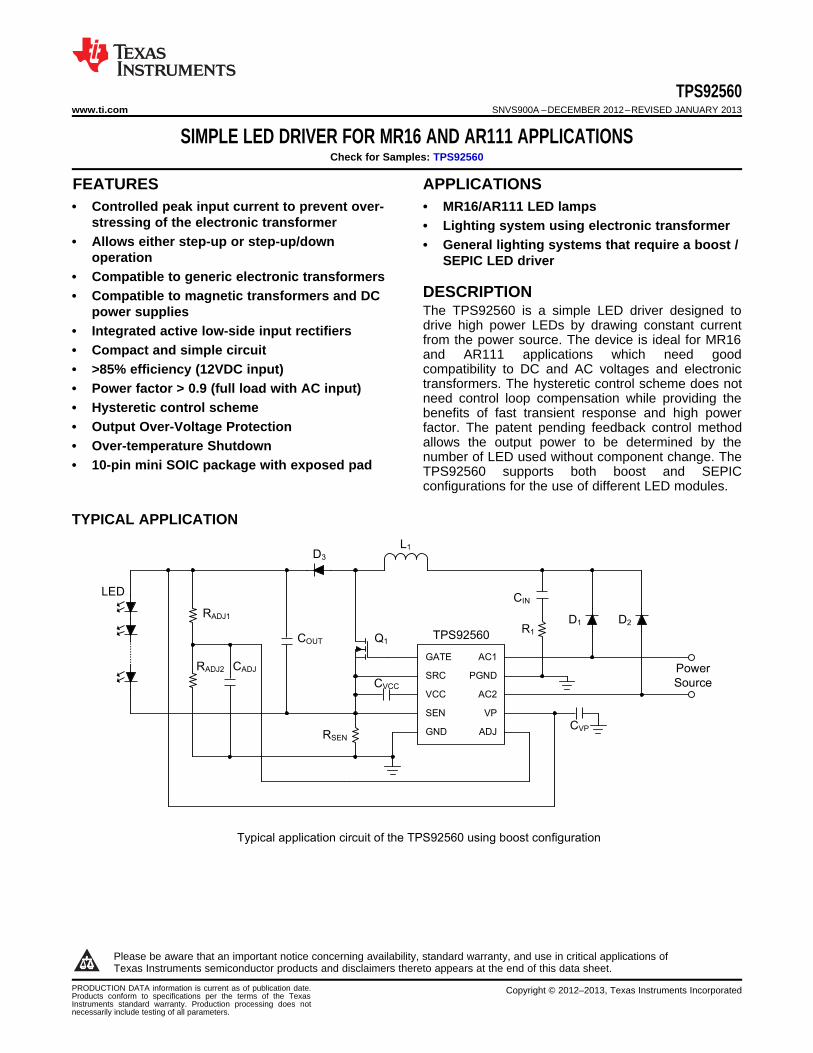
Typical application circuit of the TPS92560 using boost configuration
TPS92560www.ti.com SNVS900A –DECEMBER 2012–REVISED JANUARY 2013
SIMPLE LED DRIVER FOR MR16 AND AR111 APPLICATIONSCheck for Samples: TPS92560
1FEATURES APPLICATIONS• Controlled peak input current to prevent over- • MR16/AR111 LED lamps
stressing of the electronic transformer • Lighting system using electronic transformer• Allows either step-up or step-up/down • General lighting systems that require a boost /
operation SEPIC LED driver• Compatible to generic electronic transformers
DESCRIPTION• Compatible to magnetic transformers and DCThe TPS92560 is a simple LED driver designed topower suppliesdrive high power LEDs by drawing constant current• Integrated active low-side input rectifiersfrom the power source. The device is ideal for MR16
• Compact and simple circuit and AR111 applications which need goodcompatibility to DC and AC voltages and electronic• >85% efficiency (12VDC input)transformers. The hysteretic control scheme does not• Power factor > 0.9 (full load with AC input)need control loop compensation while providing the
• Hysteretic control scheme benefits of fast transient response and high power• Output Over-Voltage Protection factor. The patent pending feedback control method
allows the output power to be determined by the• Over-temperature Shutdownnumber of LED used without component change. The
• 10-pin mini SOIC package with exposed pad TPS92560 supports both boost and SEPICconfigurations for the use of different LED modules.
TYPICAL APPLICATION
1
Please be aware that an important notice concerning availability, standard warranty, and use in critical applications ofTexas Instruments semiconductor products and disclaimers thereto appears at the end of this data sheet.
TPS92560www.ti.com SNVS900A –DECEMBER 2012–REVISED JANUARY 2013
These devices have limited built-in ESD protection. The leads should be shorted together or the device placed in conductive foamduring storage or handling to prevent electrostatic damage to the MOS gates.
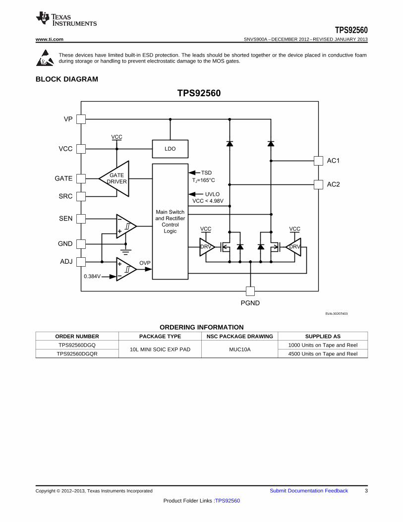
BLOCK DIAGRAM
ORDERING INFORMATIONORDER NUMBER PACKAGE TYPE NSC PACKAGE DRAWING SUPPLIED AS
TPS92560DGQ 1000 Units on Tape and Reel10L MINI SOIC EXP PAD MUC10A
TPS92560SNVS900A –DECEMBER 2012–REVISED JANUARY 2013 www.ti.com
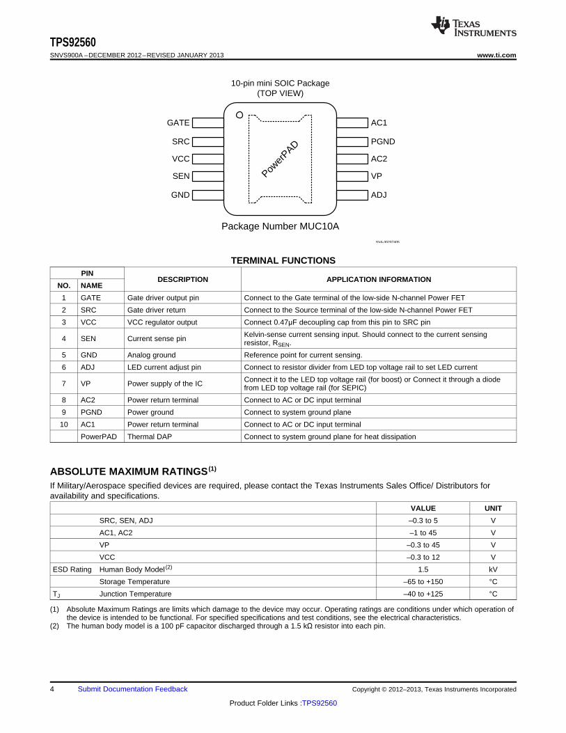
TERMINAL FUNCTIONSPIN
DESCRIPTION APPLICATION INFORMATIONNO. NAME
1 GATE Gate driver output pin Connect to the Gate terminal of the low-side N-channel Power FET
2 SRC Gate driver return Connect to the Source terminal of the low-side N-channel Power FET
3 VCC VCC regulator output Connect 0.47μF decoupling cap from this pin to SRC pin
Kelvin-sense current sensing input. Should connect to the current sensing4 SEN Current sense pin resistor, RSEN.
5 GND Analog ground Reference point for current sensing.
6 ADJ LED current adjust pin Connect to resistor divider from LED top voltage rail to set LED current
Connect it to the LED top voltage rail (for boost) or Connect it through a diode7 VP Power supply of the IC from LED top voltage rail (for SEPIC)
8 AC2 Power return terminal Connect to AC or DC input terminal
9 PGND Power ground Connect to system ground plane
10 AC1 Power return terminal Connect to AC or DC input terminal
PowerPAD Thermal DAP Connect to system ground plane for heat dissipation
ABSOLUTE MAXIMUM RATINGS (1)
If Military/Aerospace specified devices are required, please contact the Texas Instruments Sales Office/ Distributors foravailability and specifications.
VALUE UNIT
SRC, SEN, ADJ –0.3 to 5 V
AC1, AC2 –1 to 45 V
VP –0.3 to 45 V
VCC –0.3 to 12 V
ESD Rating Human Body Model (2) 1.5 kV
Storage Temperature –65 to +150 °C
TJ Junction Temperature –40 to +125 °C
(1) Absolute Maximum Ratings are limits which damage to the device may occur. Operating ratings are conditions under which operation ofthe device is intended to be functional. For specified specifications and test conditions, see the electrical characteristics.
(2) The human body model is a 100 pF capacitor discharged through a 1.5 kΩ resistor into each pin.
TPS92560www.ti.com SNVS900A –DECEMBER 2012–REVISED JANUARY 2013
RECOMMENDED OPERATING CONDITIONSover operating free-air temperature range (unless otherwise noted)
MIN NOM MAX UNIT
VP Supply voltage range 6.5 42 V
TJ Junction temperature range –40 125 °C
θJA(1) Thermal resistance, Junction to Ambient, 0 LFPM Air Flow 48 °C/W
θJC(1) Thermal resistance, Junction to Case 10 °C/W
(1) θJA and θJC measurements are performed on JEDEC boards in accordance with JESD 51-5 and JESD 51-7
ELECTRICAL CHARACTERISTICSSpecification with standard type are for TA=TJ= 25°C only; limits in boldface type apply over the full Operating JunctionTemperature (TJ) range. Minimum and Maximum are specified through test, design or statistical correlation. Typical valuesrepresent the most likely parametric norm at TJ= 25°C, and are provided for reference purposes only. Unless otherwise statedthe following conditions apply: VVP = 12V
PARAMETER TEST CONDITIONS MIN TYP MAX UNIT
SUPPLY
IIN VIN Operating current 6.5 V < VVP < 42 V 0.7 1.4 1.95 mA
VCC REGULATOR
ICC ≤ 10mA, CVCC =0.47µF7.82 8.45 9.08
12V < VVP < 42VVCC VCC Regulated Voltage (1) V
ICC = 10mA, CVCC =0.47µF VVP = 6.5V 5.22 5.8 6.18
ICC = 0mA, CVCC =0.47µF VVP = 2V 1.96 2.0
ICC-LIM VCC Current Limit VCC = 0V 6.5V < VVP < 42V 21 30 39 mA
VCC-UVLO-UPTH VCC UVLO Upper Threshold 5.0 5.38 5.76 V
VCC-UVLO-LOTH VCC UVLO Lower Threshold 4.63 4.98 5.33 V
VCC-UVLO-HYS VCC UVLO Hysteresis 190 400 640 mV
MOSFET GATE DRIVER
w.r.t. SRCVGATE-HIGH Gate Driver Output High Sinking 100mA from GATE 7.61 8.1 8.5 V
TPS92560SNVS900A –DECEMBER 2012–REVISED JANUARY 2013 www.ti.com
ELECTRICAL CHARACTERISTICS (continued)Specification with standard type are for TA=TJ= 25°C only; limits in boldface type apply over the full Operating JunctionTemperature (TJ) range. Minimum and Maximum are specified through test, design or statistical correlation. Typical valuesrepresent the most likely parametric norm at TJ= 25°C, and are provided for reference purposes only. Unless otherwise statedthe following conditions apply: VVP = 12V
PARAMETER TEST CONDITIONS MIN TYP MAX UNIT
Turn ON Voltage Threshold of AC1 andVACn-ON-TH VACn Decreasing 36 52 67 mVAC2
Turn OFF Voltage Threshold of AC1VACn-OFF-TH VACn Increasing 77 90 104 mVand AC2
VACn-TH-HYS Hysteresis Voltage of AC1 and AC2 VACn-OFF-TH - VACn-ON-TH 39 mV
IACn-OFF Off Current of AC1 and AC2 VACn = 45V 21 32 µA
TPS92560SNVS900A –DECEMBER 2012–REVISED JANUARY 2013 www.ti.com
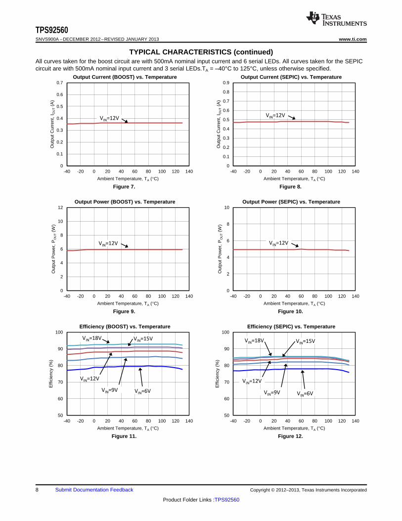
TYPICAL CHARACTERISTICS (continued)All curves taken for the boost circuit are with 500mA nominal input current and 6 serial LEDs. All curves taken for the SEPICcircuit are with 500mA nominal input current and 3 serial LEDs.TA = –40°C to 125°C, unless otherwise specified.
Output Current (BOOST) vs. Temperature Output Current (SEPIC) vs. Temperature
Figure 7. Figure 8.
Output Power (BOOST) vs. Temperature Output Power (SEPIC) vs. Temperature
Figure 9. Figure 10.
Efficiency (BOOST) vs. Temperature Efficiency (SEPIC) vs. Temperature
TPS92560www.ti.com SNVS900A –DECEMBER 2012–REVISED JANUARY 2013
OVERVIEW
The TPS92560 is a simple hysteretic control switching LED driver for MR16 or AR111 lighting applications. Thedevice accepts DC voltage, AC voltage and electronic transformer as an input power source. The compactapplication circuit can fit into a generic case of MR16 lamps easily. The hysteretic inductor current controlscheme requires no small signal control loop compensation and maintains constant average input current tosecure high compatibility to different kinds of input power source. The TPS92560 can be configured to either astep-up or step-up/down LED driver for the use of different number of LEDs. The patent pending current controlmechanism allows the use of a single set of component and PCB layout for serving different output powerrequirements by changing the number of LEDs. The integrating of the active low-side input rectifiers reduces thepower loss for voltage rectification and saves two external diodes of a generic bridge rectifier to aim for a simpleend application circuit. When the driver is used with an AC voltage source or electronic transformer, the currentregulation level increases accordingly to maintain an output current close to the level that when it is used with aDC voltage source. With the output over-voltage protection and over-temperature shutdown functions, theTPS92560 is specifically suitable for the applications that are space limited and need wide acceptance todifferent power sources.
VCC REGULATOR
The VCC pin is the output of the internal linear regulator for providing an 8.45V typical supply voltage to theMOSFET driver and internal circuits. The output current of the VCC pin is limited to 30mA typical. A low ESRceramic capacitor of 0.47μF or higher capacitance should be connected across the VCC and SRC pins to supplytransient current to the MOSFET driver.
MOSFET DRIVER
The GATE pin is the output of the gate driver which referenced to the SRC pin. The gate driver is powereddirectly by the VCC regulator which the maximum gate driving current is limited to 30mA typical. To preventhitting the VCC current limit, it is suggested to use a low gate charge MOSFET when high switching frequency isneeded.
THE ADJ PIN
The voltage on the ADJ pin determines the reference voltage for the input current regulation. Typically, the ADJpin voltage is divided from the output voltage of the circuit by a voltage divider, thus the average input current isadjusted with respect to the number of LEDs used. The voltage of the ADJ pin determines the input currentfollowing the expression:
(1)
Output Over-Voltage-Protection
In the TPS92560, a function of output Over-Voltage Protection (OVP) is provided to prevent damaging of thecircuit due to an open circuit of the LED. The OVP function is implemented to the ADJ pin. When the voltage ofthe ADJ pin exceeds 0.384V typical, the OVP circuit disables the MOSFET driver and turns off the main switch toallow the output capacitor to discharge. As the voltage of the ADJ pin decreases to below 0.353V typical, theMOSFET driver is enabled and the TPS92560 returns to normal operation. The triggering threshold of the outputvoltage is determined by the value of the resistors RADJ1 and RADJ2, which can be calculated using the followingequation:
(2)
When defining the OVP threshold voltage, it is necessary to certain that the OVP threshold voltage does notexceed the rated voltage of the output rectifier and capacitor to avoid damaging of the circuit.
TPS92560SNVS900A –DECEMBER 2012–REVISED JANUARY 2013 www.ti.com
THE AC1 AND AC2 PINS
The TPS92560 provides two internal active rectifiers for input voltage rectification. Each internal rectifier connectsacross the ACn pin to GND. These internal active rectifiers function as the low-side diode rectifiers of a genericbridge rectifier. The integrating of the active rectifiers helps in saving two external diodes of a bridge rectifieralong with an improvement of power efficiency. For high power applications, for instance, 12W output power,external diode rectifiers can be added across the ACn pin to GND to reduce heat dissipation on the TPS92560.
DETECTION OF POWER SOURCE
Figure 13. The inherent dead time of the output voltage of an electronic transformer
Both the voltages of a generic AC source (50/60Hz) and an electronic transformer carry certain amount of deadtime inherently, as shown in Figure 13. The existing of the dead time leads to a drop of the RMS input power tothe driver circuit. In order to compensate the drop of the RMS input power, the ADJ pin sources current to theresistor, RADJ2 to increase the reference voltage for the current regulation loop and in turn increase the RMSinput power accordingly when an AC voltage source or electronic transformer is detected. The output current ofthe ADJ pin for an AC input voltage and electronic transformer are 9.5μA and 11.5μA typical respectively.Practically the amount of the power for compensating the dead time of the input power source differs case tocase depending on the characteristics of the power source, the value of the RADJ1 and RADJ2 might need a fineadjustment in accordance to the characteristics of the power source. The additional output power forcompensating the dead time of the power sources (ΔPLED) are calculated using the following equations:
For 50/60Hz AC power source:
(3)
For electronic transformer:
(4)
CURRENT REGULATION
In the TPS92560, the input current regulation is attained by limiting the peak and valley of the inductor current.Practically the inductor current sensing is facilitated by detecting the voltage on the resistor, RSEN. Because thecurrent flows through the RSEN is a sum total of the currents of the main switch and LEDs, the voltage drop onthe RSEN reflects the current of the inductor that is identical to the input current to the LED driver circuit.Figure 14 shows the waveform of the inductor current ripple with the peak and valley values controlled.
TPS92560www.ti.com SNVS900A –DECEMBER 2012–REVISED JANUARY 2013
Figure 14. Inductor Current Ripple in Steady State
The voltage of the ADJ pin is determined by the forward voltage of the LED and divided from the VVP by aresistor divider. The equation for calculating the VADJ as shown in the following expression:
(5)
In steady state, the voltage drop on the RADJ1 is identical to the forward voltage of the LED (VLED) and the voltageacross the RADJ2 is identical to the voltage across the RSEN. The LED current, ILED is then calculated following theequations:
In steady state:
(6)
(7)
(8)
Since
(9)
Thus,
(10)
Put the expressions (2) to (4) into (5):
(11)
Due to the high input impedance of the ADJ pin, the current flows into the ADJ pin can be neglected and thusIRADJ1 equals IRADJ2. The LED current is then calculated following the expressions below:
(12)
Practically, the conversion efficiency of a boost circuit is almost a constant around 85%. Being assumed that theefficiency term in the ILED expression is a constant, the LED current depends solely on the magnitude of the inputvoltage, VIN. Without changing a component, the output power of the typical application circuits of the TPS92560is adjustable by using different number of LEDs.
The output power is calculated by following the expression:
[VIN - VD - IIN(nom) x (RL + RDS(ON) +RSEN + RAC-FET)] x tON
mV8.29)R1(IV1VV
1
)R1(IV5.0V
1
Rns304f
1
L
SEN)nom(ININLEDSEN)nom(ININ
SENSW
×
+×−−−
+
+×−−
×
−
=
SW
ON OFF
1f
t t=
+
x14.9mV x L
RSEN x [VLED - VIN - 1V - IIN(nom) x (1 + RSEN)]tOFF 2+ 68ns≈
x14.9mV x L
RSEN x [VIN – 0.5V - IIN(nom) x (1 + RSEN)]tON ≈ 2+ 84ns
xVSEN-LOWER-TH x L
RSEN x [VLED - VIN - 2VD - IIN(nom) x (RL +RSEN + RAC-FET)]tOFF = 2+ tRISE-PG-DELAY
xVSEN-UPPER-TH x L
RSEN x [VIN - VD - IIN(nom) x (RL + RDS(ON) +RSEN + RAC-FET)]tON = 2+ tFALL-PG-DELAY
TPS92560SNVS900A –DECEMBER 2012–REVISED JANUARY 2013 www.ti.com
SWITCHING FREQUENCY (Boost Configuration)
In the following sections, the equations and calculations are limited to the boost configuration only (i.e. the LEDforward voltage higher than the input voltage), unless otherwise specified. The application information for theSEPIC and other circuit topologies are available in separate application notes and reference designs. In theboost configuration, including the propagation delay of the control circuit, the ON and OFF times of the mainswitch are calculated following the expressions:
(14)
(15)
In the above equations, the VD is the forward voltage of D3, RL is the DC resistance of L1, RDS(ON) is the ONresistance of Q1 and RAC-FET is the turn ON resistance of the internal active rectifier with respect to the typicalapplication circuit diagram.
Practically the resistance of the RL, RDS(on) and RAC-FET is in the order if serveral tenth of mΩ, by assuming a 0.5Vdiode forward voltage and the sum total of the RL, RDS(ON) and RAC-FET is close to 1Ω, the on and off times of Q1can be approximated using the following equations:
(16)
(17)
With the switching on and OF times determined, the switching frequency can be calculated using the followingequation:
(18)
Because of the using of hysteretic control scheme, the switching frequency of the TPS92560 in steady state isdependent on the input voltage, output voltage and inductance of the inductor. Generally a 1 MHz to 1.5 MHzswitching frequency is suggested for applications using an electronic transformer as the power source.
INDUCTOR SELECTION (Boost Configuration)
Because of the using of the hysteretic control scheme, the switching frequency of the TPS92560 in a boostconfiguration can be adjusted in accordance to the value of the inductor being used. Derived from the equations(12) and (13), the value of the inductor can be determined base on the desired switching frequence by using thefollowing equation:
(19)
When selecting the inductor, it is essential to ensure the peak inductor current does not exceed the the factorysuggested saturation current of the inductor. The values of the peak and valley inductor current are calculatedusing the following equations:
[VLED - VIN - 2VD - IIN(nom) x (RL +RSEN + RAC-FET)] x tOFF
TPS92560www.ti.com SNVS900A –DECEMBER 2012–REVISED JANUARY 2013
(21)
Assume the total resistance of the RL, RDS(on) and RAC-FET is 1Ω and the diode drop, VD equal to 1V, the peakand valley currents of the inductor can be approximated using the following equations:
(22)
(23)
In order not to saturate the inductor, an inductor with a factory guranteed saturation current (ISAT) 20% higherthan the IL(peak) is suggested. Thus the ISAT of the inductor should fulfill the following requirement:
(24)
THERMAL SHUTDOWN
The TPS92560 includes a thermal shutdown circuitry that ceases the operation of the device to avoid permanentdamage. The threshold for thermal shutdown is 165°C with a 30°C hysteresis typical. During thermal shutdownthe VCC regulator is disabled and the MOSFET is turned off.
INPUT SURGE VOLTAGE PROTECTION
When use with an electronic transformer, the surge voltage across the input terminals can be sufficiently high todamage the TPS92560 depending on the charactistics of the electronic transformer. To against potentialdamaging due to the input surge voltage, a 36V zener diode can be connected across the input bridge rectifier asshown in Figure 15.
Figure 15. Input surge voltage protection using an external zener diode
TPS92560SNVS900A –DECEMBER 2012–REVISED JANUARY 2013 www.ti.com
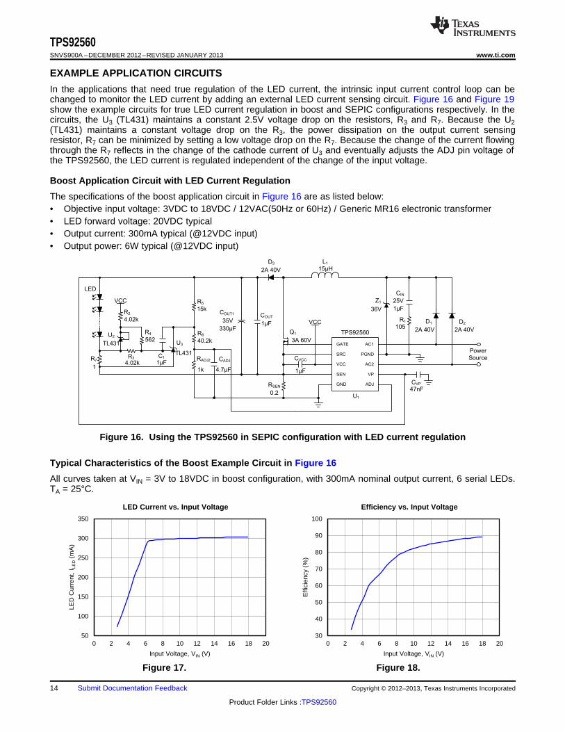
EXAMPLE APPLICATION CIRCUITS
In the applications that need true regulation of the LED current, the intrinsic input current control loop can bechanged to monitor the LED current by adding an external LED current sensing circuit. Figure 16 and Figure 19show the example circuits for true LED current regulation in boost and SEPIC configurations respectively. In thecircuits, the U3 (TL431) maintains a constant 2.5V voltage drop on the resistors, R3 and R7. Because the U2(TL431) maintains a constant voltage drop on the R3, the power dissipation on the output current sensingresistor, R7 can be minimized by setting a low voltage drop on the R7. Because the change of the current flowingthrough the R7 reflects in the change of the cathode current of U3 and eventually adjusts the ADJ pin voltage ofthe TPS92560, the LED current is regulated independent of the change of the input voltage.
Boost Application Circuit with LED Current Regulation
The specifications of the boost application circuit in Figure 16 are as listed below:• Objective input voltage: 3VDC to 18VDC / 12VAC(50Hz or 60Hz) / Generic MR16 electronic transformer• LED forward voltage: 20VDC typical• Output current: 300mA typical (@12VDC input)• Output power: 6W typical (@12VDC input)
Figure 16. Using the TPS92560 in SEPIC configuration with LED current regulation
Typical Characteristics of the Boost Example Circuit in Figure 16
All curves taken at VIN = 3V to 18VDC in boost configuration, with 300mA nominal output current, 6 serial LEDs.TA = 25°C.
LED Current vs. Input Voltage Efficiency vs. Input Voltage
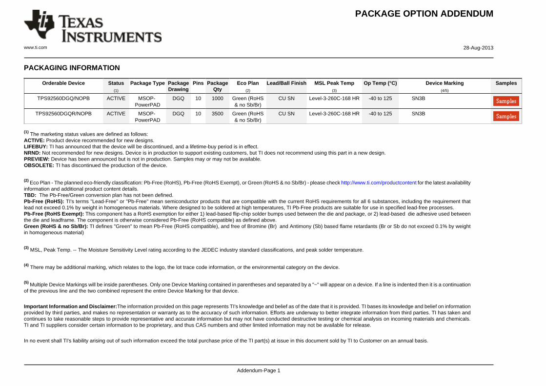
(1) The marketing status values are defined as follows:ACTIVE: Product device recommended for new designs.LIFEBUY: TI has announced that the device will be discontinued, and a lifetime-buy period is in effect.NRND: Not recommended for new designs. Device is in production to support existing customers, but TI does not recommend using this part in a new design.PREVIEW: Device has been announced but is not in production. Samples may or may not be available.OBSOLETE: TI has discontinued the production of the device.
(2) Eco Plan - The planned eco-friendly classification: Pb-Free (RoHS), Pb-Free (RoHS Exempt), or Green (RoHS & no Sb/Br) - please check http://www.ti.com/productcontent for the latest availabilityinformation and additional product content details.TBD: The Pb-Free/Green conversion plan has not been defined.Pb-Free (RoHS): TI's terms "Lead-Free" or "Pb-Free" mean semiconductor products that are compatible with the current RoHS requirements for all 6 substances, including the requirement thatlead not exceed 0.1% by weight in homogeneous materials. Where designed to be soldered at high temperatures, TI Pb-Free products are suitable for use in specified lead-free processes.Pb-Free (RoHS Exempt): This component has a RoHS exemption for either 1) lead-based flip-chip solder bumps used between the die and package, or 2) lead-based die adhesive used betweenthe die and leadframe. The component is otherwise considered Pb-Free (RoHS compatible) as defined above.Green (RoHS & no Sb/Br): TI defines "Green" to mean Pb-Free (RoHS compatible), and free of Bromine (Br) and Antimony (Sb) based flame retardants (Br or Sb do not exceed 0.1% by weightin homogeneous material)
(3) MSL, Peak Temp. -- The Moisture Sensitivity Level rating according to the JEDEC industry standard classifications, and peak solder temperature.
(4) There may be additional marking, which relates to the logo, the lot trace code information, or the environmental category on the device.
(5) Multiple Device Markings will be inside parentheses. Only one Device Marking contained in parentheses and separated by a "~" will appear on a device. If a line is indented then it is a continuationof the previous line and the two combined represent the entire Device Marking for that device.
Important Information and Disclaimer:The information provided on this page represents TI's knowledge and belief as of the date that it is provided. TI bases its knowledge and belief on informationprovided by third parties, and makes no representation or warranty as to the accuracy of such information. Efforts are underway to better integrate information from third parties. TI has taken andcontinues to take reasonable steps to provide representative and accurate information but may not have conducted destructive testing or chemical analysis on incoming materials and chemicals.TI and TI suppliers consider certain information to be proprietary, and thus CAS numbers and other limited information may not be available for release.
In no event shall TI's liability arising out of such information exceed the total purchase price of the TI part(s) at issue in this document sold by TI to Customer on an annual basis.
Texas Instruments Incorporated and its subsidiaries (TI) reserve the right to make corrections, enhancements, improvements and otherchanges to its semiconductor products and services per JESD46, latest issue, and to discontinue any product or service per JESD48, latestissue. Buyers should obtain the latest relevant information before placing orders and should verify that such information is current andcomplete. All semiconductor products (also referred to herein as “components”) are sold subject to TI’s terms and conditions of salesupplied at the time of order acknowledgment.
TI warrants performance of its components to the specifications applicable at the time of sale, in accordance with the warranty in TI’s termsand conditions of sale of semiconductor products. Testing and other quality control techniques are used to the extent TI deems necessaryto support this warranty. Except where mandated by applicable law, testing of all parameters of each component is not necessarilyperformed.
TI assumes no liability for applications assistance or the design of Buyers’ products. Buyers are responsible for their products andapplications using TI components. To minimize the risks associated with Buyers’ products and applications, Buyers should provideadequate design and operating safeguards.
TI does not warrant or represent that any license, either express or implied, is granted under any patent right, copyright, mask work right, orother intellectual property right relating to any combination, machine, or process in which TI components or services are used. Informationpublished by TI regarding third-party products or services does not constitute a license to use such products or services or a warranty orendorsement thereof. Use of such information may require a license from a third party under the patents or other intellectual property of thethird party, or a license from TI under the patents or other intellectual property of TI.
Reproduction of significant portions of TI information in TI data books or data sheets is permissible only if reproduction is without alterationand is accompanied by all associated warranties, conditions, limitations, and notices. TI is not responsible or liable for such altereddocumentation. Information of third parties may be subject to additional restrictions.
Resale of TI components or services with statements different from or beyond the parameters stated by TI for that component or servicevoids all express and any implied warranties for the associated TI component or service and is an unfair and deceptive business practice.TI is not responsible or liable for any such statements.
Buyer acknowledges and agrees that it is solely responsible for compliance with all legal, regulatory and safety-related requirementsconcerning its products, and any use of TI components in its applications, notwithstanding any applications-related information or supportthat may be provided by TI. Buyer represents and agrees that it has all the necessary expertise to create and implement safeguards whichanticipate dangerous consequences of failures, monitor failures and their consequences, lessen the likelihood of failures that might causeharm and take appropriate remedial actions. Buyer will fully indemnify TI and its representatives against any damages arising out of the useof any TI components in safety-critical applications.
In some cases, TI components may be promoted specifically to facilitate safety-related applications. With such components, TI’s goal is tohelp enable customers to design and create their own end-product solutions that meet applicable functional safety standards andrequirements. Nonetheless, such components are subject to these terms.
No TI components are authorized for use in FDA Class III (or similar life-critical medical equipment) unless authorized officers of the partieshave executed a special agreement specifically governing such use.
Only those TI components which TI has specifically designated as military grade or “enhanced plastic” are designed and intended for use inmilitary/aerospace applications or environments. Buyer acknowledges and agrees that any military or aerospace use of TI componentswhich have not been so designated is solely at the Buyer's risk, and that Buyer is solely responsible for compliance with all legal andregulatory requirements in connection with such use.
TI has specifically designated certain components as meeting ISO/TS16949 requirements, mainly for automotive use. In any case of use ofnon-designated products, TI will not be responsible for any failure to meet ISO/TS16949.
Products Applications
Audio www.ti.com/audio Automotive and Transportation www.ti.com/automotive
Amplifiers amplifier.ti.com Communications and Telecom www.ti.com/communications
Data Converters dataconverter.ti.com Computers and Peripherals www.ti.com/computers