An IMPORTANT NOTICE at the end of this data sheet addresses availability, warranty, changes, use in safety-critical applications,intellectual property matters and other important disclaimers. PRODUCTION DATA.
TPSM84203, TPSM84205, TPSM84212SLUSCV7A –JULY 2017–REVISED AUGUST 2017
TPSM84203, TPSM84205, TPSM84212 1.5-A, 28-V Input, TO-220 Power Module
1
1 Features1• Complete Integrated Power Solution• 3-Pin TO-220 Footprint• Efficiencies up to 95%• Fixed Output Voltage Options:
3.3 V, 5 V, and 12 V• 400-kHz Switching Frequency• Advanced Eco-mode™ Pulse Skip• Pre-bias Output Start-up• Over-Current Protection• Output Over-Voltage Protection• Thermal Shutdown• Operating Junction Range: –40°C to +125°C• Operating Ambient Range: –40°C to +85°C• Meets EN55022 Class B Emissions• Create a Custom Design Using the TPSM84203
3 DescriptionThe TPSM842xx power module is an easy-to-useintegrated power solution that combines a 1.5-ADC/DC converter with power MOSFETs, an inductor,and passives into a 3-pin, through-hole package. Thistotal power solution requires adding only input andoutput capacitors and eliminates the loopcompensation and magnetics part selection from thedesign process.
The standard TO-220 pin-out allows a muchimproved replacement of linear regulators packagedin this industry standard footprint. The TPSM842xxdevices provide much higher efficiency without theneed of a heatsink.
Device Information(1)
PART NUMBER PACKAGE BODY SIZE (NOM)TPSM84203
EAB 10 mm x 11 mmTPSM84205TPSM84212
(1) For all available packages, see the orderable addendum atthe end of the data sheet.
GND 2 Ground. This is the return current path for the power stage of the device. Connect this pin tothe bypass capacitors associated with VIN and VOUT.
VIN 1 I Input Voltage. This pin supplies voltage to the control circuitry and power switches of theconverter. Connect external bypass capacitors between this pin and GND.
VOUT 3 O Output Voltage. This pin is connected to the internal output inductor. Connect this pin to theoutput load and connect external bypass capacitors between this pin and GND.
(1) Stresses beyond those listed under Absolute Maximum Ratings may cause permanent damage to the device. These are stress ratingsonly, which do not imply functional operation of the device at these or any other conditions beyond those indicated under RecommendedOperating Conditions. Exposure to absolute-maximum-rated conditions for extended periods may affect device reliability.
(2) The ambient temperature is the air temperature of the surrounding environment. The junction temperature is the temperature of theinternal power IC when the device is powered. Operating below the maximum ambient temperature, as shown in the safe operating area(SOA) curves, ensures that the maximum junction temperature of any component inside the module is never exceeded.
6 Specifications
6.1 Absolute Maximum RatingsOver operating free-air temperature range (unless otherwise noted) (1)
(2) –40 125 °COperating Ambient Temperature range, TA
(2) –40 85 °CStorage temperature, Tstg –60 150 °C
(1) The ambient temperature is the air temperature of the surrounding environment. The junction temperature is the temperature of theinternal power IC when the device is powered. Operating below the maximum ambient temperature, as shown in the safe operating area(SOA) curves, ensures that the maximum junction temperature of any component inside the module is never exceeded.
6.2 Recommended Operating ConditionsOver operating free-air temperature range (unless otherwise noted)
IOUT Output current 0 1.5 ATA Operating ambient temperature range (1) –40 85 °CTJ Operating junction temperature range (1) –40 125 °C
(1) JEDEC document JEP155 states that 500-V HBM allows safe manufacturing with a standard ESD control process.(2) JEDEC document JEP157 states that 250-V CDM allows safe manufacturing with a standard ESD control process.
6.3 ESD RatingsVALUE UNIT
V(ESD) Electrostatic dischargeHuman-body model (HBM), per ANSI/ESDA/JEDEC JS-001 (1) ±2500
VCharged-device model (CDM), per JEDEC specification JESD22-C101 (2) ±1500
(1) For more information about traditional and new thermal metrics, see the Semiconductor and IC Package Thermal Metrics paper.(2) The junction-to-ambient thermal resistance, RθJA, applies to devices soldered directly to a 50 mm × 50 mm double-sided PCB with 2 oz.
copper and natural convection cooling. Additional airflow reduces RθJA.(3) The junction-to-top characterization parameter, ψJT, estimates the junction temperature, TJ, of a device in a real system, using a
procedure described in JESD51-2A (sections 6 and 7). TJ = ψJT × Pdis + TT; where Pdis is the power dissipated in the device and TT isthe temperature of the top of the controller IC.
(4) The junction-to-board characterization parameter, ψJB, estimates the junction temperature, TJ, of a device in a real system, using aprocedure described in JESD51-2A (sections 6 and 7). TJ = ψJB × Pdis + TB; where Pdis is the power dissipated in the device and TB isthe temperature of the module board 1 mm from the controller IC.
(1) The minimum input voltage is the lowest ensured voltage that will produce the nominal output voltage. See the Drop-Out Voltage sectionfor information on drop-out voltage.
(2) Specified by design. Not production tested.(3) See the efficiency graphs in the Typical Characteristics section for efficiency over the entire load range.
PARAMETER TEST CONDITIONS MIN TYP MAX UNITINPUT VOLTAGE (VIN)
VIN Input voltage range Over VOUT rangeTPSM84203 4.5 (1) 28 VTPSM84205 7 (1) 28 VTPSM84212 14.5 (1) 28 V
VIN_UVLO VIN under voltage lock outVIN increasing 4.1 4.4 VVIN decreasing 3.3 3.6 V
OUTPUT VOLTAGE (VOUT)
VOUT
Output voltage Over IOUT rangeTPSM84203 3.3 VTPSM84205 5.0 VTPSM84212 12.0 V
Set-point voltage tolerance TA = 25°C, IOUT = 0 A –3% +3%Temperature variation (2) –40°C ≤ TA ≤ 85°C, IOUT = 0 A 0.4%Line regulation Over VIN range, IOUT = 1 A 0.4%Load regulation Over IOUT range 0.5%Output voltage ripple 20 MHz bandwidth, peak-to-peak, IOUT > 500 mA 15 mV
OUTPUT CURRENT
IOUTOutput current See SOA graph for derating over temperature. 0 1.5 AOvercurrent threshold 3.1 A
PERFORMANCE
ƞ Efficiency (3)
VIN = 5 V, IOUT = 1 A VOUT = 3.3 V 92%
VIN = 12 V, IOUT = 1 AVOUT = 3.3 V 91%VOUT = 5.0 V 92%
VIN = 24 V, IOUT = 1 AVOUT = 3.3 V 87%VOUT = 5.0 V 90%VOUT = 12.0 V 94%
6.7 Typical Characteristics (VOUT = 3.3 V)Typical characteristic data has been developed from actual products tested at 25°C. This data is considered typical for thedevice. Safe operating area curves were measured using a Texas Instruments evaluation module (EVM).
6.8 Typical Characteristics (VOUT = 5 V)Typical characteristic data has been developed from actual products tested at 25°C. This data is considered typical for thedevice. Safe operating area curves were measured using a Texas Instruments evaluation module (EVM).
6.9 Typical Characteristics (VOUT = 12 V)Typical characteristic data has been developed from actual products tested at 25°C. This data is considered typical for thedevice. Safe operating area curves were measured using a Texas Instruments evaluation module (EVM).
7.1 OverviewThe TPSM84203, TPSM84205, and TPSM84212 devices are 28 V input, 1.5 A, synchronous step downconverters with PWM, MOSFETs, inductor, and control circuitry integrated into a TO-220 footprint package. Thedevice integration enables small designs, while improving efficiency over a traditional linear regulator design. TheTPSM842xx family provides fixed output voltages of 3.3 V, 5.0 V and 12.0 V. The fixed 400 kHz (typ) switchingfrequency allows small size and low output voltage ripple. Under light load conditions, these devices aredesigned to operate in high-efficiency pulse-skipping mode. These devices provide accurate voltage regulationfor a variety of loads by using a precision internal voltage reference. These devices have been designed to safelystart up into a pre-biased output voltage. Thermal shutdown and current limit features protect the device duringan overload condition. The 3-pin, TO-220 footprint package offers improved performance over traditional linearregulators packaged in the standard footprint.
(1) Consult capacitor suppliers regarding availability, material composition, RoHS and lead-free status, and manufacturing processrequirements for any capacitors identified in this table.
(2) Standard capacitance values(3) Maximum ESR @ 100kHz, 25°C.
7.3 Feature Description
7.3.1 Input CapacitorsThe TPSM842xx devices require a minimum input capacitance of 10 μF of ceramic type. High-quality ceramictype X5R or X7R capacitors with sufficient voltage rating are recommended. An additional 100 μF of non-ceramiccapacitance is recommended for applications with transient load requirements. The voltage rating of inputcapacitors must be greater than the maximum input voltage.
Table 1. Recommended Input Capacitors (1)
VENDOR SERIES PART NUMBER
CAPACITOR CHARACTERISTICS
WORKINGVOLTAGE
(V)CAPACITANCE (2)
(µF)ESR (3)
(mΩ)
Murata X7R GRM32ER71H475KA88L 50 4.7 2
TDK X5R C3225X5R1H106K250AB 50 10 3
Murata X7R GRM32ER71H106KA12 50 10 2
TDK X7R C3225X7R1H106M250AB 50 10 3
Panasonic ZA EEHZA1H101P 50 100 28
(1) Consult capacitor suppliers regarding availability, material composition, RoHS and lead-free status, and manufacturing processrequirements for any capacitors identified in this table.
(2) Standard capacitance values.(3) Maximum ESR @ 100kHz, 25°C.
7.3.2 Output CapacitorsThe TPSM84203 and TPSM84205 devices require a minimum output capacitance of 94 μF (2x 47 μF) of ceramictype. The TPSM84212 device requires a minimum output capacitance of 47 μF of ceramic type. High-quality X5Ror X7R ceramic capacitors with sufficient voltage rating are recommended. Additional output capacitance isrecommended for applications with transient load requirements. The voltage rating of output capacitors must begreater than the maximum output voltage.
7.3.3 Drop-Out VoltageThe drop-out voltage of a voltage regulator is the difference between the input voltage and the output voltagethat is required to maintain regulation. Figure 16 and Figure 17 show typical drop-out voltage graphs forTPSM84205 at ambient temperatures of 25°C and 85°C. Figure 18 and Figure 19 show typical drop-out voltagegraphs for TPSM84212 at ambient temperatures of 25°C and 85°C.
7.3.4 Internal Soft-StartThe device starts up under control of the internal soft-start function. The internal soft start time is set to 5 mstypically.
7.3.5 Safe Startup into Pre-Biased OutputsThe device has been designed to prevent the low-side MOSFET from discharging a pre-biased output. Duringmonotonic pre-biased startup, both high-side and low-side MOSFETs are not allowed to be turned on until theinternal soft-start voltage is higher than the internal feedback voltage.
7.3.6 Over-Current ProtectionThe device is protected from overcurrent conditions by cycle-by-cycle current limiting. If an output overloadcondition occurs for more than 1.28 ms, the device shuts down and restarts after approximately 40 ms. Thehiccup mode helps to reduce the device power dissipation under severe overcurrent conditions.
7.3.7 Output Over-Voltage ProtectionAn output over voltage protection circuit is incorporated to minimize output voltage overshoot when recoveringfrom output fault conditions or strong unload transients. When the output voltage goes above 108% × VOUT, thehigh-side MOSFET is forced off. When the output voltage falls below 104% × VOUT, the high-side MOSFET isenabled again.
7.3.8 Thermal ShutdownThe internal thermal-shutdown circuitry forces the device to stop switching if the junction temperature exceeds165°C typically. The device reinitiates the power-up sequence when the junction temperature drops below 155°Ctypically.
7.4 Device Functional Modes
7.4.1 Normal OperationThe TPSM842xx devices operate in Normal operation mode when the input voltage is above the minimum inputvoltage. In Normal operation mode, the device operates in continuous conduction mode (CCM) which occurswhen inductor peak current is above 840 mA typically. In CCM, the TPSM842xx devices operate at a fixedfrequency of 400 kHz (typ). In addition, to reduce EMI, the devices introduce frequency spread spectrum. Thejittering frequency range is ±6% of the switching frequency with a 780 Hz modulation rate.
7.4.2 Eco-mode™ OperationThe TPSM842xx devices operate in Eco-mode operation in light load conditions. Eco-mode is a high-efficiency,pulse-skipping mode under light load conditions. Pulse skipping initiates when the switch current falls to 840 mAtypically. During pulse skipping, the low-side FET turns off when the switch current falls to 0 A. The device takeson the characteristics of discontinuous conduction mode (DCM) operation and the apparent switching frequencydecreases. As the output current decreases, the perceived time between switching pulses increases.
NOTEInformation in the following applications sections is not part of the TI componentspecification, and TI does not warrant its accuracy or completeness. TI’s customers areresponsible for determining suitability of components for their purposes. Customers shouldvalidate and test their design implementation to confirm system functionality.
8.1 Application InformationThe TPSM842xx devices are step down DC-DC power modules. They convert a higher DC voltage to a lowerDC voltage of 3.3 V, 5 V, or 12 V with a maximum output current of 1.5 A. The following design procedure canbe used to select components for the TPSM842xx devices. Alternately, the WEBENCH® software may be usedto generate complete designs. When generating a design, the WEBENCH software utilizes an iterative designprocedure and accesses comprehensive databases of components. Please visit www.ti.com/WEBENCH for moredetails.
8.2 Typical Application
Figure 20. Typical Application
8.2.1 Design RequirementsFor this design example, use the parameters listed in Table 3 and follow the design procedures below.
Table 3. Design ParametersDESIGN PARAMETER VALUEInput Voltage VIN 24-V typicalOutput Voltage VOUT 5.0 VOutput Current Rating 1.5 AKey care-abouts TO-220 footprint, high efficiency
8.2.2.1 Custom Design With WEBENCH® ToolsClick here to create a custom design using the TPSM84203 device with the WEBENCH® Power Designer.1. Start by entering the input voltage (VIN), output voltage (VOUT), and output current (IOUT) requirements.2. Optimize the design for key parameters such as efficiency, footprint, and cost using the optimizer dial.3. Compare the generated design with other possible solutions from Texas Instruments.
The WEBENCH Power Designer provides a customized schematic along with a list of materials with real-timepricing and component availability.
In most cases, these actions are available:• Run electrical simulations to see important waveforms and circuit performance• Run thermal simulations to understand board thermal performance• Export customized schematic and layout into popular CAD formats• Print PDF reports for the design, and share the design with colleagues
Get more information about WEBENCH tools at www.ti.com/WEBENCH.
8.2.2.2 Input and Output CapacitorsThe TPSM842xx devices require both input and output capacitance for proper operation. The minimum requiredinput capacitance for all of the TPSM842xx devices is 10 µF of ceramic capacitance placed directly at the devicepins. The minimum required output capacitance for the TPSM84203 and TPSM84205 is 2× 47 µF of ceramictype. The TPSM84212 requires only one 47 µF ceramic output capacitor. Additional capacitance can be added toimprove ripple or transient response.
For this application, the minimum required input capacitance of 10 µF, ceramic was added and 2× 47 µF ceramiccapacitance was added to the output.
8.2.3.1 EMIThe TPSM842xx devices are all compliant with EN55022 Class B radiated emissions. Figure 23 to Figure 27show typical examples of radiated emissions plots for the TPSM842xx devices. The EMI plots were taken using aweb-orderable EVM with a resistive load. Input power was provided using a lead acid battery. All graphs showplots of the antenna in the horizontal and vertical positions.
9 Power Supply RecommendationsThe TPSM842xx devices are designed to operate from an input voltage supply between 4.5 V and 28 V. Thissupply must be well regulated. Proper bypassing of input supply is critical for noise performance, as is PCBlayout and grounding scheme. See the recommendations in the Layout section.
10 Layout
10.1 Layout GuidelinesTo achieve optimal electrical and thermal performance, an optimized PCB layout is required. Figure 28 shows atypical PCB layout. Some considerations for an optimized layout are:• Use large copper areas for power planes (VIN, VOUT, and GND) to minimize conduction loss and thermal
stress.• Place ceramic input and output capacitors close to the device pins to minimize high frequency noise.• Locate additional output capacitors between the ceramic capacitor and the load.• Use multiple vias to connect the power planes to internal layers.
11.1.1.1 Custom Design With WEBENCH® ToolsClick here to create a custom design using the TPSM84203 device with the WEBENCH® Power Designer.1. Start by entering the input voltage (VIN), output voltage (VOUT), and output current (IOUT) requirements.2. Optimize the design for key parameters such as efficiency, footprint, and cost using the optimizer dial.3. Compare the generated design with other possible solutions from Texas Instruments.
The WEBENCH Power Designer provides a customized schematic along with a list of materials with real-timepricing and component availability.
In most cases, these actions are available:• Run electrical simulations to see important waveforms and circuit performance• Run thermal simulations to understand board thermal performance• Export customized schematic and layout into popular CAD formats• Print PDF reports for the design, and share the design with colleagues
Get more information about WEBENCH tools at www.ti.com/WEBENCH.
11.2 Related LinksThe table below lists quick access links. Categories include technical documents, support and communityresources, tools and software, and quick access to sample or buy.
Table 4. Related Links
PARTS PRODUCT FOLDER SAMPLE & BUY TECHNICALDOCUMENTS
TOOLS &SOFTWARE
SUPPORT &COMMUNITY
TPSM84203 Click here Click here Click here Click here Click hereTPSM84205 Click here Click here Click here Click here Click hereTPSM84212 Click here Click here Click here Click here Click here
11.3 Receiving Notification of Documentation UpdatesTo receive notification of documentation updates, navigate to the device product folder on ti.com. In the upperright corner, click on Alert me to register and receive a weekly digest of any product information that haschanged. For change details, review the revision history included in any revised document.
11.4 Community ResourcesThe following links connect to TI community resources. Linked contents are provided "AS IS" by the respectivecontributors. They do not constitute TI specifications and do not necessarily reflect TI's views; see TI's Terms ofUse.
TI E2E™ Online Community TI's Engineer-to-Engineer (E2E) Community. Created to foster collaborationamong engineers. At e2e.ti.com, you can ask questions, share knowledge, explore ideas and helpsolve problems with fellow engineers.
Design Support TI's Design Support Quickly find helpful E2E forums along with design support tools andcontact information for technical support.
11.5 TrademarksEco-mode, E2E are trademarks of Texas Instruments.WEBENCH is a registered trademark of Texas Instruments.All other trademarks are the property of their respective owners.
11.6 Electrostatic Discharge CautionThis integrated circuit can be damaged by ESD. Texas Instruments recommends that all integrated circuits be handled withappropriate precautions. Failure to observe proper handling and installation procedures can cause damage.
ESD damage can range from subtle performance degradation to complete device failure. Precision integrated circuits may be moresusceptible to damage because very small parametric changes could cause the device not to meet its published specifications.
11.7 GlossarySLYZ022 — TI Glossary.
This glossary lists and explains terms, acronyms, and definitions.
12 Mechanical, Packaging, and Orderable InformationThe following pages include mechanical, packaging, and orderable information. This information is the mostcurrent data available for the designated devices. This data is subject to change without notice and revision ofthis document. For browser-based versions of this data sheet, refer to the left-hand navigation.
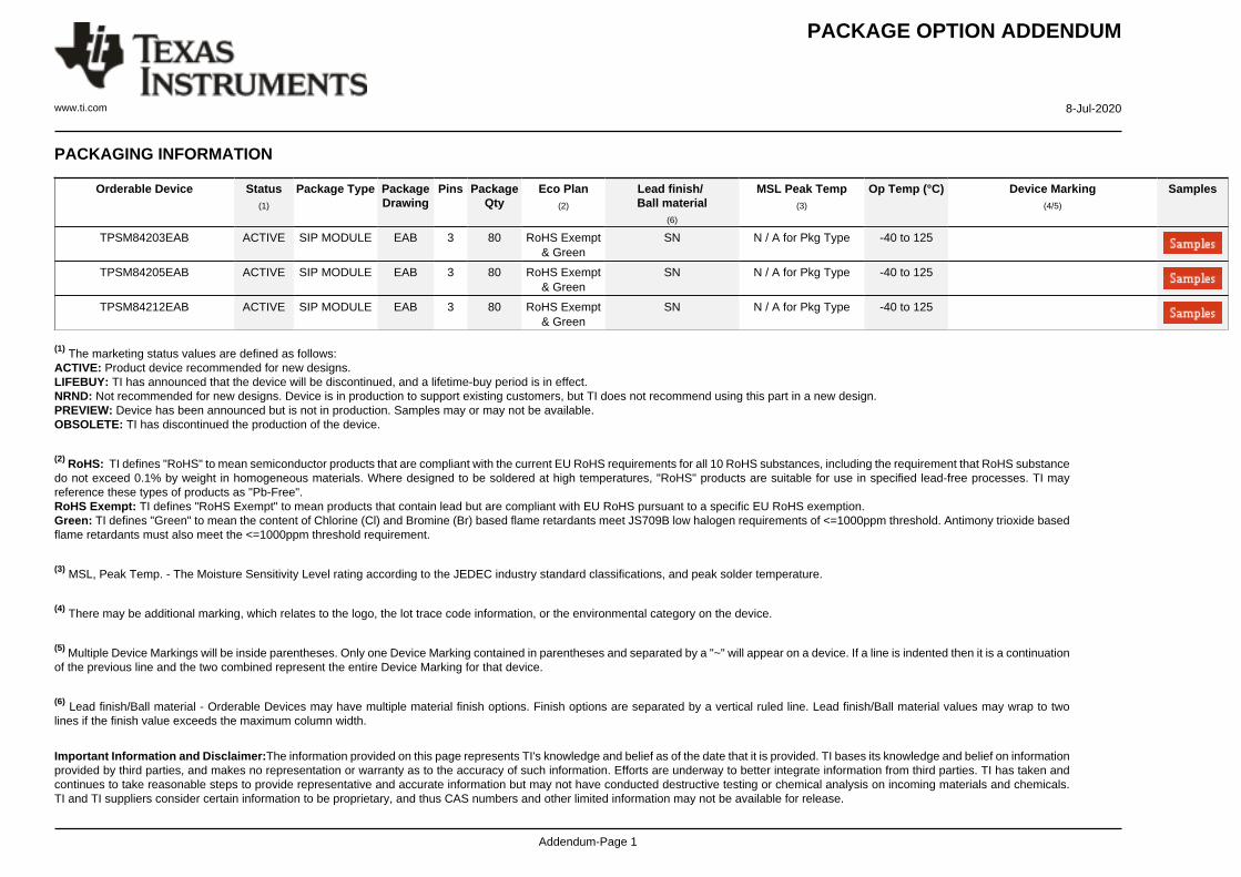
TPSM84203EAB ACTIVE SIP MODULE EAB 3 80 RoHS Exempt& Green
SN N / A for Pkg Type -40 to 125
TPSM84205EAB ACTIVE SIP MODULE EAB 3 80 RoHS Exempt& Green
SN N / A for Pkg Type -40 to 125
TPSM84212EAB ACTIVE SIP MODULE EAB 3 80 RoHS Exempt& Green
SN N / A for Pkg Type -40 to 125
(1) The marketing status values are defined as follows:ACTIVE: Product device recommended for new designs.LIFEBUY: TI has announced that the device will be discontinued, and a lifetime-buy period is in effect.NRND: Not recommended for new designs. Device is in production to support existing customers, but TI does not recommend using this part in a new design.PREVIEW: Device has been announced but is not in production. Samples may or may not be available.OBSOLETE: TI has discontinued the production of the device.
(2) RoHS: TI defines "RoHS" to mean semiconductor products that are compliant with the current EU RoHS requirements for all 10 RoHS substances, including the requirement that RoHS substancedo not exceed 0.1% by weight in homogeneous materials. Where designed to be soldered at high temperatures, "RoHS" products are suitable for use in specified lead-free processes. TI mayreference these types of products as "Pb-Free".RoHS Exempt: TI defines "RoHS Exempt" to mean products that contain lead but are compliant with EU RoHS pursuant to a specific EU RoHS exemption.Green: TI defines "Green" to mean the content of Chlorine (Cl) and Bromine (Br) based flame retardants meet JS709B low halogen requirements of <=1000ppm threshold. Antimony trioxide basedflame retardants must also meet the <=1000ppm threshold requirement.
(3) MSL, Peak Temp. - The Moisture Sensitivity Level rating according to the JEDEC industry standard classifications, and peak solder temperature.
(4) There may be additional marking, which relates to the logo, the lot trace code information, or the environmental category on the device.
(5) Multiple Device Markings will be inside parentheses. Only one Device Marking contained in parentheses and separated by a "~" will appear on a device. If a line is indented then it is a continuationof the previous line and the two combined represent the entire Device Marking for that device.
(6) Lead finish/Ball material - Orderable Devices may have multiple material finish options. Finish options are separated by a vertical ruled line. Lead finish/Ball material values may wrap to twolines if the finish value exceeds the maximum column width.
Important Information and Disclaimer:The information provided on this page represents TI's knowledge and belief as of the date that it is provided. TI bases its knowledge and belief on informationprovided by third parties, and makes no representation or warranty as to the accuracy of such information. Efforts are underway to better integrate information from third parties. TI has taken andcontinues to take reasonable steps to provide representative and accurate information but may not have conducted destructive testing or chemical analysis on incoming materials and chemicals.TI and TI suppliers consider certain information to be proprietary, and thus CAS numbers and other limited information may not be available for release.
In no event shall TI's liability arising out of such information exceed the total purchase price of the TI part(s) at issue in this document sold by TI to Customer on an annual basis.
www.ti.com
PACKAGE OUTLINE
A
C
B10.19.9
11.1 MAX
4.353.85
2X 2.543X 0.635 0.02
0.635 0.02
(1.57)
7.805.66
(1)
5.08
1.721.42
1.27 0.025
SIPMODULE - 11.1 mm max heightEAB0003ASYSTEM IN PACKAGE MODULE
4223521/C 11/2017
NOTES: 1. All linear dimensions are in millimeters. Any dimensions in parenthesis are for reference only. Dimensioning and tolerancing per ASME Y14.5M.2. This drawing is subject to change without notice.3. Location, size and quantity of each component are for reference only and may vary.
1 3
0.25 C A B
1 3
SCALE 1.000
www.ti.com
EXAMPLE BOARD LAYOUT
0.07 MAXALL AROUND
2X 0.07 MAXALL AROUND
R0.05TYP
(11)
(7.37)
(3.9)
(2.96) (2.54)
3X1.01 MIN
VIA
( 1.71)
2X ( 1.71)METAL
(5.08)
SIPMODULE - 11.1 mm max heightEAB0003ASYSTEM IN PACKAGE MODULE
4223521/C 11/2017
LAND PATTERN EXAMPLENON-SOLDER MASK DEFINED
SCALE:10X
1 2 3
SOLDER MASKOPENING
OPENING2X SOLDER MASK
RECOMMENDEDKEEP OUT AREAFOR USER COMPONENTS
IMPORTANT NOTICE AND DISCLAIMER
TI PROVIDES TECHNICAL AND RELIABILITY DATA (INCLUDING DATASHEETS), DESIGN RESOURCES (INCLUDING REFERENCE DESIGNS), APPLICATION OR OTHER DESIGN ADVICE, WEB TOOLS, SAFETY INFORMATION, AND OTHER RESOURCES “AS IS” AND WITH ALL FAULTS, AND DISCLAIMS ALL WARRANTIES, EXPRESS AND IMPLIED, INCLUDING WITHOUT LIMITATION ANY IMPLIED WARRANTIES OF MERCHANTABILITY, FITNESS FOR A PARTICULAR PURPOSE OR NON-INFRINGEMENT OF THIRD PARTY INTELLECTUAL PROPERTY RIGHTS.These resources are intended for skilled developers designing with TI products. You are solely responsible for (1) selecting the appropriate TI products for your application, (2) designing, validating and testing your application, and (3) ensuring your application meets applicable standards, and any other safety, security, or other requirements. These resources are subject to change without notice. TI grants you permission to use these resources only for development of an application that uses the TI products described in the resource. Other reproduction and display of these resources is prohibited. No license is granted to any other TI intellectual property right or to any third party intellectual property right. TI disclaims responsibility for, and you will fully indemnify TI and its representatives against, any claims, damages, costs, losses, and liabilities arising out of your use of these resources.TI’s products are provided subject to TI’s Terms of Sale (www.ti.com/legal/termsofsale.html) or other applicable terms available either on ti.com or provided in conjunction with such TI products. TI’s provision of these resources does not expand or otherwise alter TI’s applicable warranties or warranty disclaimers for TI products.


![Public Input No. 27-NFPA 92-2012 [ New Section after 1.5 ] … · 2016. 3. 29. · Public Input No. 27-NFPA 92-2012 [ New Section after 1.5 ] 1.6 Approval The design and final inspection](https://static.documents.pub/doc/80x56/60d33fe864313977436971b7/public-input-no-27-nfpa-92-2012-new-section-after-15-2016-3-29-public.jpg)
