52
101 Innovation Drive San Jose, CA 95134 www.altera.com MNL-01068-1.3 Stratix V GT Edition Reference Manual Transceiver Signal Integrity Development Kit Feedback Subscribe
101 Innovation DriveSan Jose, CA 95134www.altera.com
MNL-01068-1.3
Stratix V GT Edition Reference Manual
Transceiver Signal Integrity Development Kit
Feedback Subscribe

© 2016 Altera Corporation. All rights reserved. ALTERA, ARRIA, CYCLONE, HARDCOPY, MAX, MEGACORE, NIOS, QUARTUS and STRATIX words and logosare trademarks of Altera Corporation and registered in the U.S. Patent and Trademark Office and in other countries. All other words and logos identified astrademarks or service marks are the property of their respective holders as described at www.altera.com/common/legal.html. Altera warrants performance of itssemiconductor products to current specifications in accordance with Altera's standard warranty, but reserves the right to make changes to any products andservices at any time without notice. Altera assumes no responsibility or liability arising out of the application or use of any information, product, or servicedescribed herein except as expressly agreed to in writing by Altera. Altera customers are advised to obtain the latest version of device specifications before relyingon any published information and before placing orders for products or services.
January 2016 Altera Corporation Transceiver Signal Integrity Development KitStratix V GT Edition Reference Manual
ISO 9001:2008 Registered
January 2016 Altera Corporation
Contents
Chapter 1. OverviewGeneral Description . . . . . . . . . . . . . . . . . . . . . . . . . . . . . . . . . . . . . . . . . . . . . . . . . . . . . . . . . . . . . . . . . . . . . 1–1Board Component Blocks . . . . . . . . . . . . . . . . . . . . . . . . . . . . . . . . . . . . . . . . . . . . . . . . . . . . . . . . . . . . . . . . . 1–1Development Board Block Diagram . . . . . . . . . . . . . . . . . . . . . . . . . . . . . . . . . . . . . . . . . . . . . . . . . . . . . . . . 1–4Handling the Board . . . . . . . . . . . . . . . . . . . . . . . . . . . . . . . . . . . . . . . . . . . . . . . . . . . . . . . . . . . . . . . . . . . . . . 1–4
Chapter 2. Board ComponentsBoard Overview . . . . . . . . . . . . . . . . . . . . . . . . . . . . . . . . . . . . . . . . . . . . . . . . . . . . . . . . . . . . . . . . . . . . . . . . . 2–2Featured Device: Stratix V GT FPGA . . . . . . . . . . . . . . . . . . . . . . . . . . . . . . . . . . . . . . . . . . . . . . . . . . . . . . . 2–6
I/O Resources . . . . . . . . . . . . . . . . . . . . . . . . . . . . . . . . . . . . . . . . . . . . . . . . . . . . . . . . . . . . . . . . . . . . . . . . 2–6MAX II CPLD System Controller . . . . . . . . . . . . . . . . . . . . . . . . . . . . . . . . . . . . . . . . . . . . . . . . . . . . . . . . . . 2–9Configuration, Status, and Setup Elements . . . . . . . . . . . . . . . . . . . . . . . . . . . . . . . . . . . . . . . . . . . . . . . . . 2–14
Configuration . . . . . . . . . . . . . . . . . . . . . . . . . . . . . . . . . . . . . . . . . . . . . . . . . . . . . . . . . . . . . . . . . . . . . . . 2–14FPGA Programming over Embedded USB-Blaster . . . . . . . . . . . . . . . . . . . . . . . . . . . . . . . . . . . . . 2–14FPGA Programming from Flash Memory . . . . . . . . . . . . . . . . . . . . . . . . . . . . . . . . . . . . . . . . . . . . . 2–15FPGA Programming over External USB-Blaster . . . . . . . . . . . . . . . . . . . . . . . . . . . . . . . . . . . . . . . . 2–17JTAG Header . . . . . . . . . . . . . . . . . . . . . . . . . . . . . . . . . . . . . . . . . . . . . . . . . . . . . . . . . . . . . . . . . . . . . 2–17
Status Elements . . . . . . . . . . . . . . . . . . . . . . . . . . . . . . . . . . . . . . . . . . . . . . . . . . . . . . . . . . . . . . . . . . . . . . 2–18Status LEDs . . . . . . . . . . . . . . . . . . . . . . . . . . . . . . . . . . . . . . . . . . . . . . . . . . . . . . . . . . . . . . . . . . . . . . . 2–18
Setup Elements . . . . . . . . . . . . . . . . . . . . . . . . . . . . . . . . . . . . . . . . . . . . . . . . . . . . . . . . . . . . . . . . . . . . . . 2–19FPP Configuration/MAX II Bypass DIP Switch . . . . . . . . . . . . . . . . . . . . . . . . . . . . . . . . . . . . . . . . 2–19Program Select Jumper . . . . . . . . . . . . . . . . . . . . . . . . . . . . . . . . . . . . . . . . . . . . . . . . . . . . . . . . . . . . . 2–20Reset Push Button . . . . . . . . . . . . . . . . . . . . . . . . . . . . . . . . . . . . . . . . . . . . . . . . . . . . . . . . . . . . . . . . . 2–20CPU Reset Push Button . . . . . . . . . . . . . . . . . . . . . . . . . . . . . . . . . . . . . . . . . . . . . . . . . . . . . . . . . . . . . 2–20
Clock Circuitry . . . . . . . . . . . . . . . . . . . . . . . . . . . . . . . . . . . . . . . . . . . . . . . . . . . . . . . . . . . . . . . . . . . . . . . . . 2–21Dedicated Transceiver Clocks . . . . . . . . . . . . . . . . . . . . . . . . . . . . . . . . . . . . . . . . . . . . . . . . . . . . . . . . . 2–21General-Purpose Clocks . . . . . . . . . . . . . . . . . . . . . . . . . . . . . . . . . . . . . . . . . . . . . . . . . . . . . . . . . . . . . . 2–22Embedded USB-Blaster Clocks . . . . . . . . . . . . . . . . . . . . . . . . . . . . . . . . . . . . . . . . . . . . . . . . . . . . . . . . . 2–23
Transceiver Channels . . . . . . . . . . . . . . . . . . . . . . . . . . . . . . . . . . . . . . . . . . . . . . . . . . . . . . . . . . . . . . . . . . . 2–23Backplane Connectors . . . . . . . . . . . . . . . . . . . . . . . . . . . . . . . . . . . . . . . . . . . . . . . . . . . . . . . . . . . . . . . . . . 2–25General User Input/Output . . . . . . . . . . . . . . . . . . . . . . . . . . . . . . . . . . . . . . . . . . . . . . . . . . . . . . . . . . . . . 2–28
User-Defined Push Buttons . . . . . . . . . . . . . . . . . . . . . . . . . . . . . . . . . . . . . . . . . . . . . . . . . . . . . . . . . . . . 2–28User-Defined DIP Switch . . . . . . . . . . . . . . . . . . . . . . . . . . . . . . . . . . . . . . . . . . . . . . . . . . . . . . . . . . . . . 2–29User-Defined LEDs . . . . . . . . . . . . . . . . . . . . . . . . . . . . . . . . . . . . . . . . . . . . . . . . . . . . . . . . . . . . . . . . . . . 2–29Character LCD . . . . . . . . . . . . . . . . . . . . . . . . . . . . . . . . . . . . . . . . . . . . . . . . . . . . . . . . . . . . . . . . . . . . . . 2–30
Components and Interfaces . . . . . . . . . . . . . . . . . . . . . . . . . . . . . . . . . . . . . . . . . . . . . . . . . . . . . . . . . . . . . . 2–3210/100/1000 Ethernet . . . . . . . . . . . . . . . . . . . . . . . . . . . . . . . . . . . . . . . . . . . . . . . . . . . . . . . . . . . . . . . . 2–32Transceiver Interfaces . . . . . . . . . . . . . . . . . . . . . . . . . . . . . . . . . . . . . . . . . . . . . . . . . . . . . . . . . . . . . . . . 2–34
XFP Interface . . . . . . . . . . . . . . . . . . . . . . . . . . . . . . . . . . . . . . . . . . . . . . . . . . . . . . . . . . . . . . . . . . . . . 2–34SFP+ Interface . . . . . . . . . . . . . . . . . . . . . . . . . . . . . . . . . . . . . . . . . . . . . . . . . . . . . . . . . . . . . . . . . . . . . 2–35
Flash Memory . . . . . . . . . . . . . . . . . . . . . . . . . . . . . . . . . . . . . . . . . . . . . . . . . . . . . . . . . . . . . . . . . . . . . . . . . 2–36Power Supply . . . . . . . . . . . . . . . . . . . . . . . . . . . . . . . . . . . . . . . . . . . . . . . . . . . . . . . . . . . . . . . . . . . . . . . . . . 2–37
Power Measurement . . . . . . . . . . . . . . . . . . . . . . . . . . . . . . . . . . . . . . . . . . . . . . . . . . . . . . . . . . . . . . . . . 2–39Power Distribution System . . . . . . . . . . . . . . . . . . . . . . . . . . . . . . . . . . . . . . . . . . . . . . . . . . . . . . . . . . . . 2–40Temperature Sense . . . . . . . . . . . . . . . . . . . . . . . . . . . . . . . . . . . . . . . . . . . . . . . . . . . . . . . . . . . . . . . . . . . 2–41
Statement of China-RoHS Compliance . . . . . . . . . . . . . . . . . . . . . . . . . . . . . . . . . . . . . . . . . . . . . . . . . . . . 2–42
Additional Information
Transceiver Signal Integrity Development KitStratix V GT Edition Reference Manual

iv ContentsContents
Board Revision History . . . . . . . . . . . . . . . . . . . . . . . . . . . . . . . . . . . . . . . . . . . . . . . . . . . . . . . . . . . . . . . . . . 1–1Document Revision History . . . . . . . . . . . . . . . . . . . . . . . . . . . . . . . . . . . . . . . . . . . . . . . . . . . . . . . . . . . . . . 1–1How to Contact Altera . . . . . . . . . . . . . . . . . . . . . . . . . . . . . . . . . . . . . . . . . . . . . . . . . . . . . . . . . . . . . . . . . . . 1–1Typographic Conventions . . . . . . . . . . . . . . . . . . . . . . . . . . . . . . . . . . . . . . . . . . . . . . . . . . . . . . . . . . . . . . . . 1–2
Transceiver Signal Integrity Development Kit January 2016 Altera CorporationStratix V GT Edition Reference Manual

January 2016 Altera Corporation
1. Overview
This document describes the hardware features of the Stratix® V GT transceiver signal integrity development board, including the detailed pin-out and component reference information required to create custom FPGA designs that interface with all components of the board.
General DescriptionThe Transceiver Signal Integrity Development Kit, Stratix V GT Edition, allows you to evaluate the performance of the Stratix V GT FPGA which is optimized for high-performance and high-bandwidth applications with integrated transceivers supporting backplane, chip-to-chip, and chip-to-module operation.
f For more information on the following topics, refer to the respective documents:
■ Setting up the development board and using the included software, refer to the Transceiver Signal Integrity Development Kit, Stratix V GT Edition User Guide.
■ Stratix V device family, refer to the Stratix V Device Handbook.
Board Component BlocksThe Stratix V GT transceiver signal integrity development board provides a hardware platform for evaluating the performance and signal integrity features of the Altera® Stratix V GT device. The development board features the following major component blocks:
■ Altera Stratix V GT FPGA (5SGTMC7K3F40C2) in a 1517-pin FineLine BGA package
■ 622,000 LEs
■ 234,720 adaptive logic modules (ALMs)
■ 50-Mbits (Mb) embedded memory
■ 512 18x18-bit multipliers
■ 36 transceivers (32 channels with 12.5 Gbps and four channels with 28 Gbps)
■ 174 LVDS transmit channels
■ 28 phase locked loops (PLLs)
■ 696 user I/Os
■ 850-mV core voltage
Transceiver Signal Integrity Development KitStratix V GT Edition Reference Manual

1–2 Chapter 1: OverviewBoard Component Blocks
■ FPGA configuration circuitry
■ MAX® II CPLD (EPM2210F256C3N) and flash Fast Passive Parallel (FPP) configuration
■ MAX II CPLD (EPM570M100C4N) for on-board USB-BlasterTM to use with the Quartus® II Programmer
■ JTAG header for external USB-Blaster
■ Flash storage for two configuration images (factory and user)
■ On-Board clocking circuitry
■ 625-MHz, 644.53125-MHz, 706.25-MHz, and 875-MHz programmable oscillators for the high-speed transceiver reference clocks
■ 25/100/125/200 MHz jumper-selectable oscillator to the FPGA
■ 50-MHz general-purpose oscillator to the FPGA
■ One differential SMA clock input to the FPGA
■ Four differential SMA clock input to the transceivers
■ Spread spectrum clock input
■ Four clock trigger outputs
■ Transceiver interfaces
■ Four 25.78-Gbps TX/RX channels to MMPX connectors (for Stratix V GT FPGA only)
■ Seven 12.5-Gbps TX/RX channels to SMA connectors
■ One 12.5-Gbps TX/RX channel to SFP+ cage
■ One 12.5-Gbps TX/RX channel to XFP cage
■ Seven 12.5-Gbps TX/RX channels to Molex backplane connectors
■ Seven 12.5-Gbps TX/RX channels to Amphenol backplane connectors
■ Seven 12.5-Gbps TX/RX channels to Tyco backplane connectors
■ Memory devices
■ One 1-Gbit (Gb) synchronous flash with a 16-bit data bus
■ Communication ports
■ USB type-B connector
■ Gigabit Ethernet port and RJ-45 jack
■ LCD header
■ General user I/O
■ Eight user LEDs
■ Three configuration status LEDs (factory, user, error)
■ Six Ethernet LEDs
■ One 16-character × 2-line character LCD display
Transceiver Signal Integrity Development Kit January 2016 Altera CorporationStratix V GT Edition Reference Manual
Chapter 1: Overview 1–3Board Component Blocks
■ Push button and DIP switches
■ One CPU reset push button
■ One configuration reset push button
■ Four general user push buttons
■ One 8-position user DIP switch
■ One 6-position MSEL control DIP switch
■ One 4-position frequency select and spread spectrum select DIP switch
■ One 4-position transceiver clock input select DIP switch
■ Two 4-position power sequence enable select DIP switches
■ One 4-position VCCRT_GXB/VCCA_GXB voltage select DIP switch
■ Heat sink and fan
■ 40-mm heat sink and fan combo
■ One over-temperature warning indicator LED
■ Power
■ 14-V – 20-V (laptop) DC input
■ One power-on LED
■ One on/off power slide switch
■ Power monitor and trim capability
■ Power sequence capability
■ System Monitoring
■ Temperature—FPGA die
■ Mechanical
■ 7.5" x 10.5" board dimension
January 2016 Altera Corporation Transceiver Signal Integrity Development KitStratix V GT Edition Reference Manual
1–4 Chapter 1: OverviewDevelopment Board Block Diagram
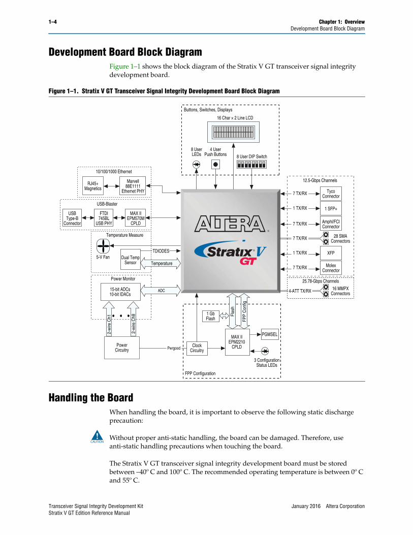
Development Board Block DiagramFigure 1–1 shows the block diagram of the Stratix V GT transceiver signal integrity development board.
Handling the BoardWhen handling the board, it is important to observe the following static discharge precaution:
c Without proper anti-static handling, the board can be damaged. Therefore, use anti-static handling precautions when touching the board.
The Stratix V GT transceiver signal integrity development board must be stored between –40º C and 100º C. The recommended operating temperature is between 0º C and 55º C.
Figure 1–1. Stratix V GT Transceiver Signal Integrity Development Board Block Diagram
LCD
Buttons, Switches, Displays
16 Char × 2 Line LCD
8 User DIP Switch
4 UserPush Buttons
8 UserLEDs
Pwrgood
FPP Configuration
25.78-Gbps Channels
12.5-Gbps Channels
ClockCircuitry
TycoConnector
1 SFP+
XFP
Amphl/FCIConnector
28 SMAConnectors
16 MMPXConnectors
MolexConnector
1 GbFlash
3 ConfigurationStatus LEDs
MAX IIEPM2210
CPLD
PGMSEL
Flas
h
FPP
Con
fig
Power Monitor
15-bit ADCs10-bit IDACs
ADC
2-w
ire C
h1
PowerCircuitry
2-w
ire C
h8
TemperatureDual Temp
Sensor
Temperature Measure
TDIODES
7 TX/RX
1 TX/RX
7 TX/RX
7 TX/RX
1 TX/RX
7 TX/RX
4-ATT TX/RX
5-V Fan
USB-Blaster
USBType-B
Connector
FTDI745BL
USB PHY
MAX IIEPM570M
CPLD
10/100/1000 Ethernet
RJ45+Magnetics
Marvell88E1111
Ethernet PHY
Transceiver Signal Integrity Development Kit January 2016 Altera CorporationStratix V GT Edition Reference Manual

January 2016 Altera Corporation
2. Board Components
This chapter introduces all the important components on the Stratix V GT transceiver signal integrity development board. Figure 2–1 illustrates major component locations and Table 2–1 provides a brief description of all features of the board.
1 A complete set of schematics, a physical layout database, and GERBER files for the development board reside in the Stratix V GT development kit documents directory.
f For information about powering up the board and installing the demo software, refer to the Transceiver Signal Integrity Development Kit, Stratix V GT Edition User Guide.
This chapter consists of the following sections:
■ “Board Overview”
■ “Featured Device: Stratix V GT FPGA” on page 2–6
■ “MAX II CPLD System Controller” on page 2–9
■ “Configuration, Status, and Setup Elements” on page 2–14
■ “Clock Circuitry” on page 2–21
■ “General User Input/Output” on page 2–28
■ “Components and Interfaces” on page 2–32
■ “Flash Memory” on page 2–36
■ “Power Supply” on page 2–37
■ “Statement of China-RoHS Compliance” on page 2–42
Transceiver Signal Integrity Development KitStratix V GT Edition Reference Manual

2–2 Chapter 2: Board ComponentsBoard Overview
Board OverviewThis section provides an overview of the Stratix V GT transceiver signal integrity development board, including an annotated board image and component descriptions. Figure 2–1 provides an overview of the development board features.
Table 2–1 describes the components and lists their corresponding board references.
Figure 2–1. Overview of the Stratix V GT Transceiver Signal Integrity Development Board Features
User DIP Switch (SW4)
Stratix V GTFPGA (U29)
VCCRT_GXB/ VCCA_GXBVoltage Select (SW2)
MSEL Selection/MAX II Bypass (S7)
Clock TriggerOutputs(U32, U33)
Clock TriggerOutputs(U34, U35)
Transceiver Clock Input Select DIP switch (SW6)
Reset Push Buttons (S5, S6)
MAX IICPLD (U19)
MMPXConnectors
Transceiver InputReference Clocks
User PushButtons(SW1-SW4)User LEDs(D8-D15)
SFP+Module(J51)
XFP Module(U25)
MolexBackplaneConnector(J34)
TycoConnector
(J33)
Amphenol Backplane Connector (J32)
PowerSwitch(SW1)
JTAG Header(J93)
DC PowerJack (J1)
Character LCD (J30)
EmbeddedUSB-Blaster
(CN1)
Power SequenceEnable/Disable
(SW7, SW3)
10/100 /1000Ethernet
Port (J29)
Fan Connector (J12)Fan Jumper (J26)
Fan LED (D6)
GXB Receive SMA
GXB Transmit SMAFPGA Clock Input Select/Spread Spectrum Clock Select
(SW5)
External PowerInput Banana Jacks(J6, J15, J18, J21)
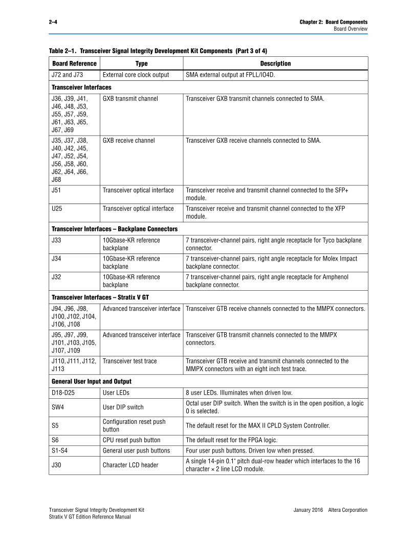
Table 2–1. Transceiver Signal Integrity Development Kit Components (Part 1 of 4)
Board Reference Type Description
Featured Devices
U29 FPGA Stratix V GT FPGA (5SGTMC7K3F40C2), 1517-pin BGA.
U19 CPLD MAX II CPLD (EPM2210F256C3N), 256-pin BGA.
Configuration, Status, and Setup Elements
S7 (pin 6-7) MAX II bypass switch Enables or disables the MAX II CPLD in the JTAG chain. The MAX II CPLD is disabled by default.
Transceiver Signal Integrity Development Kit January 2016 Altera CorporationStratix V GT Edition Reference Manual

Chapter 2: Board Components 2–3Board Overview
J28 Program select jumper Toggles the program LEDs to select which FPGA image to load on power-up; 0 selects factory image and 1 selects user-defined image.
S7 FPP configuration/MAX II bypass DIP switch Select the configuration mode from the MAX II CPLD.
SW5 Spread spectrum clock settings DIP switch
Sets the spread spectrum output clock frequency and down-spread percentages.
SW2 (pin2-7)VCCA_GXB voltage selection jumper
Selects VCCA voltage to the FPGA. When the jumper is set to close position, the VCCA voltage is 3.0 V (default). When set to open position, the VCCA voltage is 2.5 V.
SW2 (pin 1-8)VCCRT voltage selection jumper
Selects VCCRT voltage to the FPGA. When the jumper is set to close position, the VCCRT voltage is 1.0 V (default). When set to open position, the VCCRT voltage is 0.85 V.
J26Fan control jumper Selects whether the fan is always on or the FPGA automatically
controls the fan. To set it to its default setting of always on, connect jumper pin 2-3. Connect jumper pin 1-2 to set the fan in auto mode.
D7 Fan LED Indicates an over-temperature condition in the FPGA and a fan should be attached to the FPGA and running.
D8 Load LED Illuminates during embedded USB-Blaster data transfers.
D9 Error LED Illuminates when the FPGA configuration from flash fails.
D3 Power LED Illuminates when 14-V power is present.
D12-D17 Ethernet LEDs Indicates the connection speed as well as transmit or receive activity.
Clock Circuitry
Y3 Programmable oscillator
Feeds even-numbered REFCLKs on left side of the Stratix V GT device and trigger an output at board reference J81. The external input is available at board reference J79 and J80. The default frequency is 644.53125 MHz.
Y4 Programmable oscillator
Feeds odd-numbered REFCLKs on left side of the Stratix V GT device and trigger an output at board reference J85. The external input is available at board reference J83 and J84. The default frequency is 706.25 MHz.
Y5 Programmable oscillator
Feeds even-numbered REFCLKs on right side of the Stratix V GT device and trigger an output at board reference J88. The external input is available at board reference J86 and J87. The default frequency is 625 MHz.
Y6 Programmable oscillator
Feeds odd-numbered REFCLKs on right side of the Stratix V GT device and trigger an output at board reference J91. The external input is available at board reference J89 and J90. The default frequency is 875 MHz.
SW6 Transceiver clock input select DIP switch Selects the SMA or oscillator as the clock input.
Y2 50-MHz oscillator 50.000-MHz crystal oscillator for general purpose logic.
X3 25/100/125/200-MHz core clock selectable oscillator
Selects the core clock frequency. The default frequency is 100 MHz.
SW5 Spread spectrum selection switch
Select either the core or spread spectrum clock. Pin 1-2 selects S0 and S1 while pin 3-4 selects SS0 and SS1.
J70 and J71 External core clock input SMA external input at CLK10 p/n.
Table 2–1. Transceiver Signal Integrity Development Kit Components (Part 2 of 4)
Board Reference Type Description
January 2016 Altera Corporation Transceiver Signal Integrity Development KitStratix V GT Edition Reference Manual
2–4 Chapter 2: Board ComponentsBoard Overview
J72 and J73 External core clock output SMA external output at FPLL/IO4D.
Transceiver Interfaces
J36, J39, J41, J46, J48, J53, J55, J57, J59, J61, J63, J65, J67, J69
GXB transmit channel Transceiver GXB transmit channels connected to SMA.
J35, J37, J38, J40, J42, J45, J47, J52, J54, J56, J58, J60, J62, J64, J66, J68
GXB receive channel Transceiver GXB receive channels connected to SMA.
J51 Transceiver optical interface Transceiver receive and transmit channel connected to the SFP+ module.
U25 Transceiver optical interface Transceiver receive and transmit channel connected to the XFP module.
Transceiver Interfaces – Backplane Connectors
J33 10Gbase-KR reference backplane
7 transceiver-channel pairs, right angle receptacle for Tyco backplane connector.
J34 10Gbase-KR reference backplane
7 transceiver-channel pairs, right angle receptacle for Molex Impact backplane connector.
J32 10Gbase-KR reference backplane
7 transceiver-channel pairs, right angle receptacle for Amphenol backplane connector.
Transceiver Interfaces – Stratix V GT
J94, J96, J98, J100, J102, J104, J106, J108
Advanced transceiver interface Transceiver GTB receive channels connected to the MMPX connectors.
J95, J97, J99, J101, J103, J105, J107, J109
Advanced transceiver interface Transceiver GTB transmit channels connected to the MMPX connectors.
J110, J111, J112, J113
Transceiver test trace Transceiver GTB receive and transmit channels connected to the MMPX connectors with an eight inch test trace.
General User Input and Output
D18-D25 User LEDs 8 user LEDs. Illuminates when driven low.
SW4 User DIP switch Octal user DIP switch. When the switch is in the open position, a logic 0 is selected.
S5 Configuration reset push button The default reset for the MAX II CPLD System Controller.
S6 CPU reset push button The default reset for the FPGA logic.
S1-S4 General user push buttons Four user push buttons. Driven low when pressed.
J30 Character LCD header A single 14-pin 0.1" pitch dual-row header which interfaces to the 16 character × 2 line LCD module.
Table 2–1. Transceiver Signal Integrity Development Kit Components (Part 3 of 4)
Board Reference Type Description
Transceiver Signal Integrity Development Kit January 2016 Altera CorporationStratix V GT Edition Reference Manual
Chapter 2: Board Components 2–5Board Overview
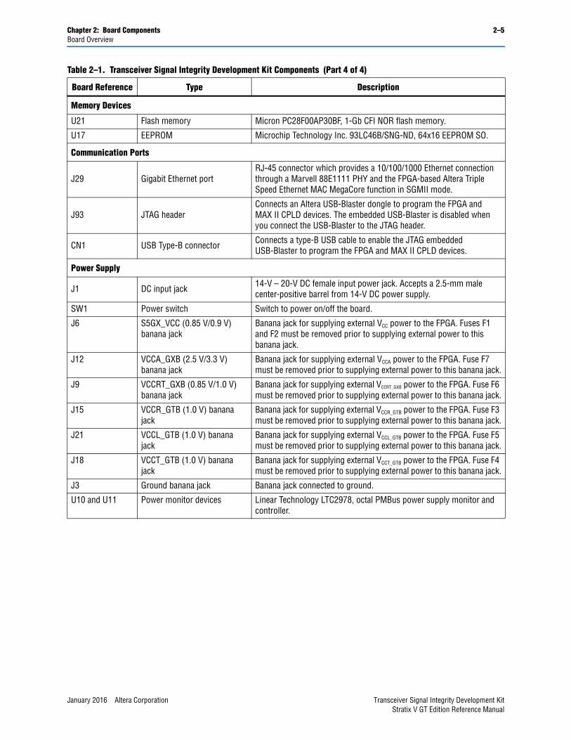
Memory Devices
U21 Flash memory Micron PC28F00AP30BF, 1-Gb CFI NOR flash memory.
U17 EEPROM Microchip Technology Inc. 93LC46B/SNG-ND, 64x16 EEPROM SO.
Communication Ports
J29 Gigabit Ethernet portRJ-45 connector which provides a 10/100/1000 Ethernet connection through a Marvell 88E1111 PHY and the FPGA-based Altera Triple Speed Ethernet MAC MegaCore function in SGMII mode.
J93 JTAG headerConnects an Altera USB-Blaster dongle to program the FPGA and MAX II CPLD devices. The embedded USB-Blaster is disabled when you connect the USB-Blaster to the JTAG header.
CN1 USB Type-B connector Connects a type-B USB cable to enable the JTAG embedded USB-Blaster to program the FPGA and MAX II CPLD devices.
Power Supply
J1 DC input jack 14-V – 20-V DC female input power jack. Accepts a 2.5-mm male center-positive barrel from 14-V DC power supply.
SW1 Power switch Switch to power on/off the board.
J6 S5GX_VCC (0.85 V/0.9 V) banana jack
Banana jack for supplying external VCC power to the FPGA. Fuses F1 and F2 must be removed prior to supplying external power to this banana jack.
J12 VCCA_GXB (2.5 V/3.3 V) banana jack
Banana jack for supplying external VCCA power to the FPGA. Fuse F7 must be removed prior to supplying external power to this banana jack.
J9 VCCRT_GXB (0.85 V/1.0 V) banana jack
Banana jack for supplying external VCCRT_GXB power to the FPGA. Fuse F6 must be removed prior to supplying external power to this banana jack.
J15 VCCR_GTB (1.0 V) banana jack
Banana jack for supplying external VCCR_GTB power to the FPGA. Fuse F3 must be removed prior to supplying external power to this banana jack.
J21 VCCL_GTB (1.0 V) banana jack
Banana jack for supplying external VCCL_GTB power to the FPGA. Fuse F5 must be removed prior to supplying external power to this banana jack.
J18 VCCT_GTB (1.0 V) banana jack
Banana jack for supplying external VCCT_GTB power to the FPGA. Fuse F4 must be removed prior to supplying external power to this banana jack.
J3 Ground banana jack Banana jack connected to ground.
U10 and U11 Power monitor devices Linear Technology LTC2978, octal PMBus power supply monitor and controller.
Table 2–1. Transceiver Signal Integrity Development Kit Components (Part 4 of 4)
Board Reference Type Description
January 2016 Altera Corporation Transceiver Signal Integrity Development KitStratix V GT Edition Reference Manual
2–6 Chapter 2: Board ComponentsFeatured Device: Stratix V GT FPGA
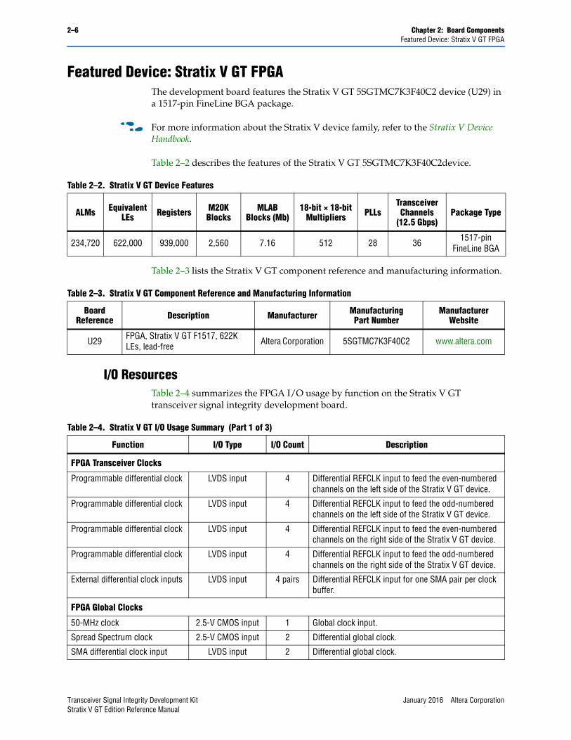
Featured Device: Stratix V GT FPGAThe development board features the Stratix V GT 5SGTMC7K3F40C2 device (U29) in a 1517-pin FineLine BGA package.
f For more information about the Stratix V device family, refer to the Stratix V Device Handbook.
Table 2–2 describes the features of the Stratix V GT 5SGTMC7K3F40C2device.
Table 2–3 lists the Stratix V GT component reference and manufacturing information.
I/O ResourcesTable 2–4 summarizes the FPGA I/O usage by function on the Stratix V GT transceiver signal integrity development board.
Table 2–2. Stratix V GT Device Features
ALMs Equivalent LEs Registers M20K
BlocksMLAB
Blocks (Mb)18-bit × 18-bit
Multipliers PLLsTransceiver Channels
(12.5 Gbps)Package Type
234,720 622,000 939,000 2,560 7.16 512 28 36 1517-pin FineLine BGA
Table 2–3. Stratix V GT Component Reference and Manufacturing Information
Board Reference Description Manufacturer Manufacturing
Part NumberManufacturer
Website
U29 FPGA, Stratix V GT F1517, 622K LEs, lead-free Altera Corporation 5SGTMC7K3F40C2 www.altera.com
Table 2–4. Stratix V GT I/O Usage Summary (Part 1 of 3)
Function I/O Type I/O Count Description
FPGA Transceiver Clocks
Programmable differential clock LVDS input 4 Differential REFCLK input to feed the even-numbered channels on the left side of the Stratix V GT device.
Programmable differential clock LVDS input 4 Differential REFCLK input to feed the odd-numbered channels on the left side of the Stratix V GT device.
Programmable differential clock LVDS input 4 Differential REFCLK input to feed the even-numbered channels on the right side of the Stratix V GT device.
Programmable differential clock LVDS input 4 Differential REFCLK input to feed the odd-numbered channels on the right side of the Stratix V GT device.
External differential clock inputs LVDS input 4 pairs Differential REFCLK input for one SMA pair per clock buffer.
FPGA Global Clocks
50-MHz clock 2.5-V CMOS input 1 Global clock input.
Spread Spectrum clock 2.5-V CMOS input 2 Differential global clock.
SMA differential clock input LVDS input 2 Differential global clock.
Transceiver Signal Integrity Development Kit January 2016 Altera CorporationStratix V GT Edition Reference Manual

Chapter 2: Board Components 2–7Featured Device: Stratix V GT FPGA
Temperature Monitor
Temperature sense diodes Analog 2 Stratix V GT internal sense diode.
Power Monitor Devices
LTC2978 controller 2.5-V CMOS 24 Octal PMBus power supply monitor and controller.
Temperature Measure
MAX1619 interface 2.5V CMOS 4 Die and ambient temperature sense.
Fan
FAN_On 2.5-V CMOS output 1 Fan control
FAN_LED 2.5-V CMOS output 1 Fan LED
USB-Blaster
JTAG USB-Blaster or JTAG header
2.5-V CMOS 4 Built-in USB-Blaster or JTAG 0.1-mm header for debugging
FPP Configuration
FPGA Dclk 2.5-V CMOS input 1 FPP Dclk
FPGA D[15:0] 2.5V CMOS 16 FPP data bus
MSEL [4:0] 2.5V CMOS 5 Dedicated configuration pins
NCONFIG 2.5V CMOS 1 Dedicated configuration pins
NSTATUS 2.5V CMOS 1 Dedicated configuration pins
NCE 2.5V CMOS 1 Dedicated configuration pins
CONFIG_DONE 2.5V CMOS 1 Dedicated configuration pins
Flash Memory
ADDR[26:1] 1.8-V CMOS output 26 Flash address bus
DATA[15:0] 1.8-V CMOS input/output
16 Flash data bus
FLASH_CEn 1.8-V CMOS output 1 Flash chip enable
FLASH_OEn 1.8-V CMOS output 1 Flash read strobe
FLASH_WEn 1.8-V CMOS output 1 Flash write strobe
FLASH_WAIT 1.8-V CMOS input 1 Flash ready or busy
FLASH_CLK 1.8-V CMOS output 1 Flash clock
FLASH_RSTn 1.8-V CMOS output 1 Flash reset
FLASH_ADVn 1.8-V CMOS output 1 Flash address valid
FLASH_WPn 1.8-V CMOS output 1 Flash write protect
Reset
CPU_RESETn 2.5-V CMOS input 1 Nios® II CPU reset
Switches, Buttons, LEDS
User push buttons 2.5-V CMOS input 4 4 user push buttons
User DIP switches 2.5-V CMOS input 8 8 user DIP switches
User LEDs 2.5-V CMOS output 8 8 user LEDs (green)
Table 2–4. Stratix V GT I/O Usage Summary (Part 2 of 3)
Function I/O Type I/O Count Description
January 2016 Altera Corporation Transceiver Signal Integrity Development KitStratix V GT Edition Reference Manual
2–8 Chapter 2: Board ComponentsFeatured Device: Stratix V GT FPGA
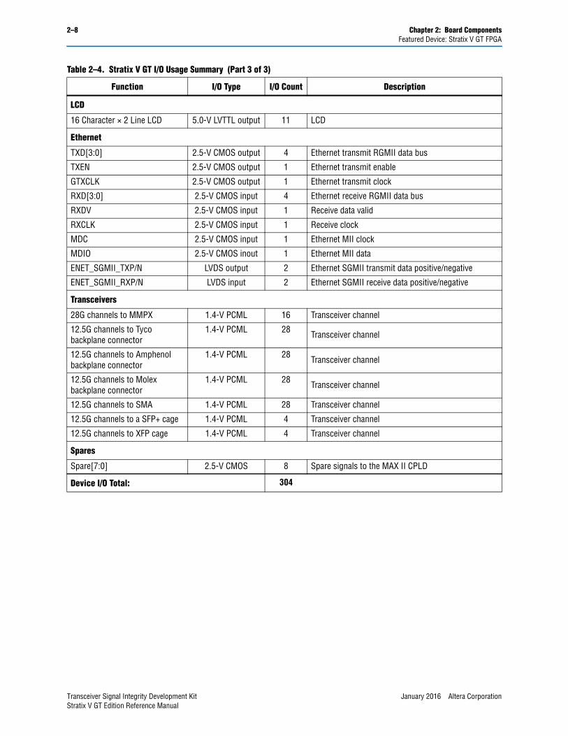
LCD
16 Character × 2 Line LCD 5.0-V LVTTL output 11 LCD
Ethernet
TXD[3:0] 2.5-V CMOS output 4 Ethernet transmit RGMII data bus
TXEN 2.5-V CMOS output 1 Ethernet transmit enable
GTXCLK 2.5-V CMOS output 1 Ethernet transmit clock
RXD[3:0] 2.5-V CMOS input 4 Ethernet receive RGMII data bus
RXDV 2.5-V CMOS input 1 Receive data valid
RXCLK 2.5-V CMOS input 1 Receive clock
MDC 2.5-V CMOS input 1 Ethernet MII clock
MDIO 2.5-V CMOS inout 1 Ethernet MII data
ENET_SGMII_TXP/N LVDS output 2 Ethernet SGMII transmit data positive/negative
ENET_SGMII_RXP/N LVDS input 2 Ethernet SGMII receive data positive/negative
Transceivers
28G channels to MMPX 1.4-V PCML 16 Transceiver channel
12.5G channels to Tyco backplane connector
1.4-V PCML 28 Transceiver channel
12.5G channels to Amphenol backplane connector
1.4-V PCML 28 Transceiver channel
12.5G channels to Molex backplane connector
1.4-V PCML 28 Transceiver channel
12.5G channels to SMA 1.4-V PCML 28 Transceiver channel
12.5G channels to a SFP+ cage 1.4-V PCML 4 Transceiver channel
12.5G channels to XFP cage 1.4-V PCML 4 Transceiver channel
Spares
Spare[7:0] 2.5-V CMOS 8 Spare signals to the MAX II CPLD
Device I/O Total: 304
Table 2–4. Stratix V GT I/O Usage Summary (Part 3 of 3)
Function I/O Type I/O Count Description
Transceiver Signal Integrity Development Kit January 2016 Altera CorporationStratix V GT Edition Reference Manual

Chapter 2: Board Components 2–9MAX II CPLD System Controller
MAX II CPLD System Controller The board utilizes the EPM2210F256C3N System Controller, an Altera MAX II CPLD, for the following purposes:
■ FPGA configuration from flash memory
■ Temperature monitoring
■ Fan control
■ Virtual JTAG interface for PC-based power and temperature GUI
■ Control registers for clocks
■ Control registers for remote system update
■ Register with CPLD design revision and board information (read-only)
Figure 2–2 illustrates the MAX II CPLD System Controller's functionality and external circuit connections as a block diagram.
Table 2–5 lists the I/O signals present on the MAX II CPLD System Controller. The signal names and functions are relative to the MAX II device (U19).
Figure 2–2. MAX II CPLD System Controller Block Diagram
MAX1619Controller
Information Register
EmbeddedUSB-Blaster
MAX II CPLD
SLD-HUB
PFL
FSD Bus
TemperatureMeasure Results
Virtual-JTAG
PC
S5_VCCAMeasure Results
FPGA
LTC2978Controller
Flash
GPIO
Decoder Encoder
JTAG Control
ControlRegister
Power Monitor
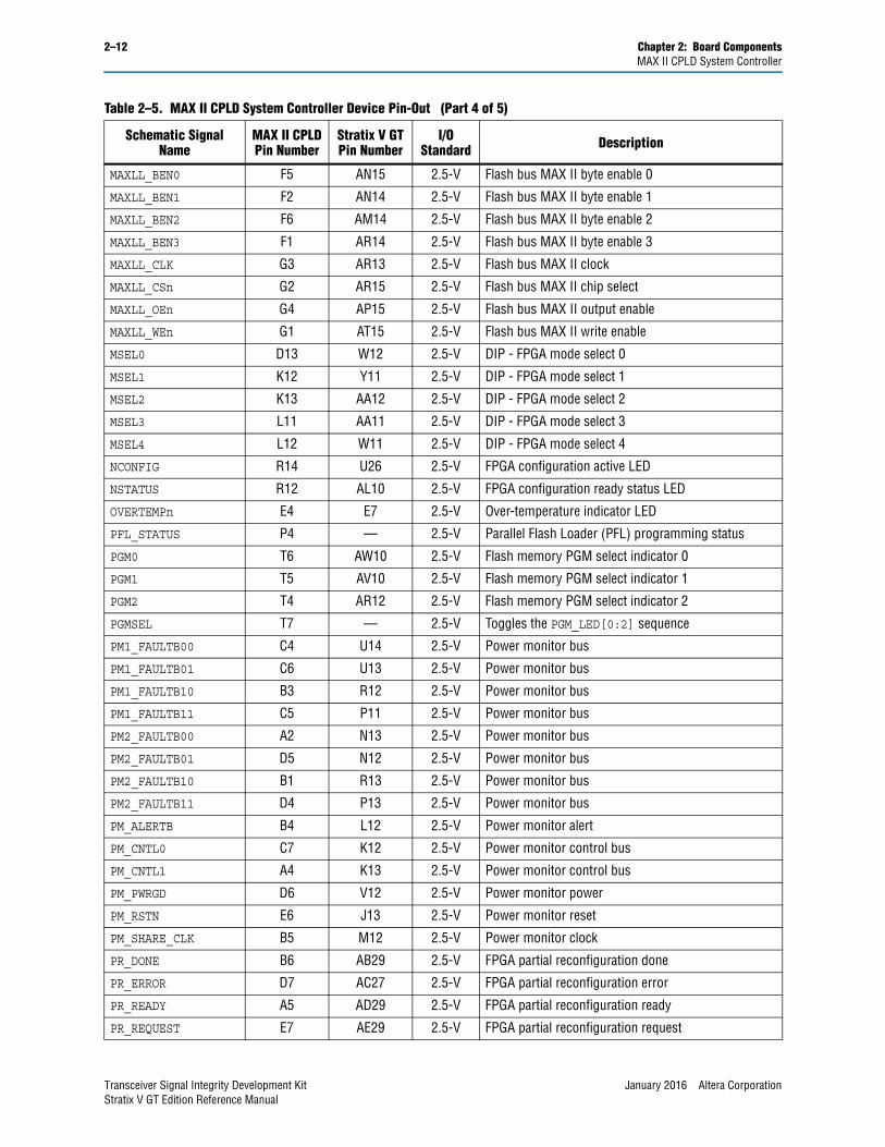
Table 2–5. MAX II CPLD System Controller Device Pin-Out (Part 1 of 5)
Schematic Signal Name
MAX II CPLDPin Number
Stratix V GT Pin Number
I/O Standard Description
50MHZ_MAXLL_CLK H5 — 2.5-V 50 MHz clock input
ALERTn D2 E8 2.5-V Temperature monitor alert
CONF_DONE T13 AB12 2.5-V Configuration done
CONFIG_D0 T11 AR33 2.5-V Configuration data
CONFIG_D1 T10 AU32 2.5-V Configuration data
January 2016 Altera Corporation Transceiver Signal Integrity Development KitStratix V GT Edition Reference Manual

2–10 Chapter 2: Board ComponentsMAX II CPLD System Controller
CONFIG_D2 P12 AT32 2.5-V Configuration data
CONFIG_D3 P11 AW32 2.5-V Configuration data
CONFIG_D4 R11 AV32 2.5-V Configuration data
CONFIG_D5 R10 AM32 2.5-V Configuration data
CONFIG_D6 N12 AL31 2.5-V Configuration data
CONFIG_D7 P10 AN32 2.5-V Configuration data
CONFIG_D8 H4 AN31 2.5-V Configuration data
CONFIG_D9 J4 AM31 2.5-V Configuration data
CONFIG_D10 J3 AL30 2.5-V Configuration data
CONFIG_D11 K2 AK30 2.5-V Configuration data
CONFIG_D12 K5 AJ30 2.5-V Configuration data
CONFIG_D13 K4 AJ29 2.5-V Configuration data
CONFIG_D14 K3 AJ28 2.5-V Configuration data
CONFIG_D15 L5 AM29 2.5-V Configuration data
CONFIG_ERR R9 — 2.5-V Configuration error
DCLK T8 U28 2.5-V Configuration clock
ENET_RSTn A15 AT6 2.5-V Ethernet LED
F_AD1 M16 AE14 2.5-V Flash address bus
F_AD2 M15 AD14 2.5-V Flash address bus
F_AD3 M14 AC13 2.5-V Flash address bus
F_AD4 N16 AC12 2.5-V Flash address bus
F_AD5 N15 AG14 2.5-V Flash address bus
F_AD6 J16 AF14 2.5-V Flash address bus
F_AD7 N13 AD11 2.5-V Flash address bus
F_AD8 N14 AC11 2.5-V Flash address bus
F_AD9 C14 AF11 2.5-V Flash address bus
F_AD10 B12 AE11 2.5-V Flash address bus
F_AD11 F15 AE13 2.5-V Flash address bus
F_AD12 F16 AE12 2.5-V Flash address bus
F_AD13 D16 AJ14 2.5-V Flash address bus
F_AD14 A11 AH13 2.5-V Flash address bus
F_AD15 A12 AG13 2.5-V Flash address bus
F_AD16 B13 AF13 2.5-V Flash address bus
F_AD17 E15 AJ13 2.5-V Flash address bus
F_AD18 L14 AJ12 2.5-V Flash address bus
F_AD19 J15 AH12 2.5-V Flash address bus
F_AD20 D14 AG11 2.5-V Flash address bus
F_AD21 K14 AK12 2.5-V Flash address bus
F_AD22 D15 AK11 2.5-V Flash address bus
Table 2–5. MAX II CPLD System Controller Device Pin-Out (Part 2 of 5)
Schematic Signal Name
MAX II CPLDPin Number
Stratix V GT Pin Number
I/O Standard Description
Transceiver Signal Integrity Development Kit January 2016 Altera CorporationStratix V GT Edition Reference Manual

Chapter 2: Board Components 2–11MAX II CPLD System Controller
F_AD23 A13 AL12 2.5-V Flash address bus
F_AD24 B14 AL11 2.5-V Flash address bus
F_AD25 C13 AM13 2.5-V Flash address bus
F_AD26 B16 AL13 2.5-V Flash address bus
F_ADVn P13 AP7 2.5-V Flash address valid
F_BSYn J14 AR7 2.5-V Flash chip busy
F_CEn P14 AP9 2.5-V Flash chip enable
F_CLK R16 AN6 2.5-V Flash clock
F_D0 L15 AN11 2.5-V Flash data bus
F_D1 L16 AM11 2.5-V Flash data bus
F_D2 K15 AP12 2.5-V Flash data bus
F_D3 K16 AN12 2.5-V Flash data bus
F_D4 H16 AN10 2.5-V Flash data bus
F_D5 H15 AM10 2.5-V Flash data bus
F_D6 G16 AR11 2.5-V Flash data bus
F_D7 G15 AR10 2.5-V Flash data bus
F_D8 M13 AT12 2.5-V Flash data bus
F_D9 L13 AU13 2.5-V Flash data bus
F_D10 J13 AU12 2.5-V Flash data bus
F_D11 H13 AU11 2.5-V Flash data bus
F_D12 G13 AT11 2.5-V Flash data bus
F_D13 F13 AW13 2.5-V Flash data bus
F_D14 F14 AV13 2.5-V Flash data bus
F_D15 E14 AW11 2.5-V Flash data bus
F_OEn P15 AN9 2.5-V Flash output enable
F_RSTn H14 AL8 2.5-V Flash reset
F_WEn G14 AM8 2.5-V Flash write enable
F_WPn T12 AP6 2.5-V Flash write protect
FACTORY_IMAGE R8 — 2.5-V Factory image for configuration
FAN_CTRL E3 D6 2.5-V Fan control
FAN_LED C3 C6 2.5-V Fan LED
INIT_DONE R13 AN33 2.5-V FPGA initialization done.
JTAG_TCK P3 AV34 2.5-V JTAG chain clock
JTAG_TMS N4 AU34 2.5-V JTAG chain mode
MAX_2_MAX_INITDONE H2 — 2.5-VControl signal between the MAX II System Controller and the MAX II embedded USB-Blaster to indicate that initialization is done.
MAX_FPP_TDI L6 — 2.5-V Fast Passive Parallel (FPP) programming data in
MAX_FPP_TDO M5 — 2.5-V FPP programming data out
Table 2–5. MAX II CPLD System Controller Device Pin-Out (Part 3 of 5)
Schematic Signal Name
MAX II CPLDPin Number
Stratix V GT Pin Number
I/O Standard Description
January 2016 Altera Corporation Transceiver Signal Integrity Development KitStratix V GT Edition Reference Manual
2–12 Chapter 2: Board ComponentsMAX II CPLD System Controller
MAXLL_BEN0 F5 AN15 2.5-V Flash bus MAX II byte enable 0
MAXLL_BEN1 F2 AN14 2.5-V Flash bus MAX II byte enable 1
MAXLL_BEN2 F6 AM14 2.5-V Flash bus MAX II byte enable 2
MAXLL_BEN3 F1 AR14 2.5-V Flash bus MAX II byte enable 3
MAXLL_CLK G3 AR13 2.5-V Flash bus MAX II clock
MAXLL_CSn G2 AR15 2.5-V Flash bus MAX II chip select
MAXLL_OEn G4 AP15 2.5-V Flash bus MAX II output enable
MAXLL_WEn G1 AT15 2.5-V Flash bus MAX II write enable
MSEL0 D13 W12 2.5-V DIP - FPGA mode select 0
MSEL1 K12 Y11 2.5-V DIP - FPGA mode select 1
MSEL2 K13 AA12 2.5-V DIP - FPGA mode select 2
MSEL3 L11 AA11 2.5-V DIP - FPGA mode select 3
MSEL4 L12 W11 2.5-V DIP - FPGA mode select 4
NCONFIG R14 U26 2.5-V FPGA configuration active LED
NSTATUS R12 AL10 2.5-V FPGA configuration ready status LED
OVERTEMPn E4 E7 2.5-V Over-temperature indicator LED
PFL_STATUS P4 — 2.5-V Parallel Flash Loader (PFL) programming status
PGM0 T6 AW10 2.5-V Flash memory PGM select indicator 0
PGM1 T5 AV10 2.5-V Flash memory PGM select indicator 1
PGM2 T4 AR12 2.5-V Flash memory PGM select indicator 2
PGMSEL T7 — 2.5-V Toggles the PGM_LED[0:2] sequence
PM1_FAULTB00 C4 U14 2.5-V Power monitor bus
PM1_FAULTB01 C6 U13 2.5-V Power monitor bus
PM1_FAULTB10 B3 R12 2.5-V Power monitor bus
PM1_FAULTB11 C5 P11 2.5-V Power monitor bus
PM2_FAULTB00 A2 N13 2.5-V Power monitor bus
PM2_FAULTB01 D5 N12 2.5-V Power monitor bus
PM2_FAULTB10 B1 R13 2.5-V Power monitor bus
PM2_FAULTB11 D4 P13 2.5-V Power monitor bus
PM_ALERTB B4 L12 2.5-V Power monitor alert
PM_CNTL0 C7 K12 2.5-V Power monitor control bus
PM_CNTL1 A4 K13 2.5-V Power monitor control bus
PM_PWRGD D6 V12 2.5-V Power monitor power
PM_RSTN E6 J13 2.5-V Power monitor reset
PM_SHARE_CLK B5 M12 2.5-V Power monitor clock
PR_DONE B6 AB29 2.5-V FPGA partial reconfiguration done
PR_ERROR D7 AC27 2.5-V FPGA partial reconfiguration error
PR_READY A5 AD29 2.5-V FPGA partial reconfiguration ready
PR_REQUEST E7 AE29 2.5-V FPGA partial reconfiguration request
Table 2–5. MAX II CPLD System Controller Device Pin-Out (Part 4 of 5)
Schematic Signal Name
MAX II CPLDPin Number
Stratix V GT Pin Number
I/O Standard Description
Transceiver Signal Integrity Development Kit January 2016 Altera CorporationStratix V GT Edition Reference Manual

Chapter 2: Board Components 2–13MAX II CPLD System Controller
PWR_GOOD J1 — — Power good signal to indicate that all voltage rails have come up to their proper levels.
RESETN T2 — 2.5-V FPGA reset LED
S5_RSTN T15 AV19 2.5-V FPGA reset
S5_SMBCLK_TEMP D3 B8 2.5-V Temperature monitor SMB clock
S5_SMBDATA_TEMP C2 A8 2.5-V Temperature monitor SMB data
SCL_OSC D8 — 2.5-V Configuration clock oscillator
SCL_PM C8 L11 2.5-V Configuration clock power monitor
SDA_OSC B7 — 2.5-V Configuration data oscillator
SDA_PM A6 M11 2.5-V Configuration data power monitor
SPARE0 A10 AH19 2.5-V Spare signals to the MAX II CPLD
SPARE1 A9 AG19 2.5-V Spare signals to the MAX II CPLD
SPARE2 A8 AJ18 2.5-V Spare signals to the MAX II CPLD
SPARE3 A7 AH18 2.5-V Spare signals to the MAX II CPLD
SPARE4 B11 AN19 2.5-V Spare signals to the MAX II CPLD
SPARE5 B10 AM19 2.5-V Spare signals to the MAX II CPLD
SPARE6 B9 AR19 2.5-V Spare signals to the MAX II CPLD
SPARE7 B8 AP19 2.5-V Spare signals to the MAX II CPLD
USB_MAX_D0 M3 — 2.5-V USB configuration data bus
USB_MAX_D1 L4 — 2.5-V USB configuration data bus
USB_MAX_D2 N1 — 2.5-V USB configuration data bus
USB_MAX_D3 L3 — 2.5-V USB configuration data bus
USB_MAX_D4 N2 — 2.5-V USB configuration data bus
USB_MAX_D5 M4 — 2.5-V USB configuration data bus
USB_MAX_D6 N3 — 2.5-V USB configuration data bus
USB_MAX_D7 P2 — 2.5-V USB configuration data bus
USB_MAX_PWR_ENn E1 — 2.5-V USB configuration power enable
USB_MAX_RDn D1 — 2.5-V USB configuration read from FIFO
USB_MAX_RXFn F4 — 2.5-V USB configuration receive enable
USB_MAX_TXEn E2 — 2.5-V USB configuration transmit enable
USB_MAX_WR F3 — 2.5-V USB configuration write to FIFO
USER_IMAGE R7 — 2.5-V User image for configuration
Table 2–5. MAX II CPLD System Controller Device Pin-Out (Part 5 of 5)
Schematic Signal Name
MAX II CPLDPin Number
Stratix V GT Pin Number
I/O Standard Description
January 2016 Altera Corporation Transceiver Signal Integrity Development KitStratix V GT Edition Reference Manual

2–14 Chapter 2: Board ComponentsConfiguration, Status, and Setup Elements
Table 2–6 lists the MAX II CPLD System Controller component reference and manufacturing information.
Configuration, Status, and Setup ElementsThis section describes the board's configuration, status, and setup elements.
ConfigurationThis section describes the FPGA, flash memory, and MAX II CPLD System Controller device programming methods supported by the Stratix V GT transceiver signal integrity development board.
The Stratix V GT transceiver signal integrity development board supports three configuration methods:
■ Embedded USB-Blaster is the default method for configuring the FPGA at any time using the Quartus II Programmer in JTAG mode with the supplied USB cable.
■ MAX II and flash FPP download for configuring the FPGA using stored images from the flash on either power-up or pressing the reset push-button (S5).
■ JTAG header (J93) for initial debugging and to bring up the on-board USB-Blaster circuitry.
FPGA Programming over Embedded USB-BlasterProgramming the FPGA over embedded USB-Blaster is implemented using a type-B USB connector (CN1), a USB 2.0 PHY device, and an Altera MAX II CPLD EPM2210F256C3N (U19). This allows configuration of the FPGA using a USB cable that connects directly between the USB port on the board (CN1) and a USB port of a PC running the Quartus II software. The embedded USB-Blaster in the MAX II CPLD System Controller acts as a master to the JTAG chain.
A green USB-Blaster LED (D8) indicates the USB-Blaster activity. The embedded USB-Blaster is automatically disabled when you connect an external USB-Blaster to the JTAG chain at the JTAG header (J93).
Table 2–6. MAX II CPLD EPM2210 System Controller Component Reference and Manufacturing Information
Board Reference Description Manufacturer ManufacturingPart Number
Manufacturer Website
U19 MAX II CPLD 256FBGA -3 LF 3.3 V VCCINT Altera Corporation EPM2210F256C3N www.altera.com
Transceiver Signal Integrity Development Kit January 2016 Altera CorporationStratix V GT Edition Reference Manual

Chapter 2: Board Components 2–15Configuration, Status, and Setup Elements
Figure 2–3 shows the block diagram for the embedded USB-Blaster connection.
MAX II CPLD System Controller
The EPM570M100 MAX II CPLD (U16) is dedicated to the on-board USB-Blaster functionality. The CPLD connects to the FT245BL USB FIFO device on one side and drives the JTAG signals out the other side on the general purpose I/O (GPIO) pins. A 64x16 EEPROM connects to the CPLD device and stores the factory image for USB–JTAG functionality.
FPGA Programming from Flash MemoryOn power-up, the MAX II CPLD System Controller’s parallel flash loader (PFL) configures the FPGA from the flash memory. The system controller uses the Altera Parallel Flash Loader (PFL) megafunction to read 16-bit data from the flash memory and converts it to FPP format. This 8-bit data is then written to the FPGA’s dedicated configuration pins during configuration.
The FPP configuration is implemented with an Altera MAX II CPLD together with the Micron PC2800AP30BF 1-Gb CFI NOR-type flash device (U21). The CPLD shares the flash interface with the FPGA. The configuration program select (PGMSEL) jumper (J28), selects between two Programmer Object Files (.pof) files (factory or user) stored in the flash. The configuration mode select signals, MSEL[4:0], are pulled to [00100] FPP x16 on the board for FPP mode configuration.
There are three configuration status LEDs, CONFIG_ERR, FACTORY_IMAGE, and USER_IMAGE (D9, D10, D11) that indicate the status of the FPP configuration. For information on the configuration status LEDs, refer to “Status Elements” on page 2–18.
Table 2–7 lists the PGMSEL jumper settings.
Figure 2–3. Embedded USB-Blaster Connection
USB
USB Type-BConnector
USB 2.0 PHYUSB FIFO BUS
MAX IICPLD JTAG
JTAG
JTAG Header
Stratix V GTFPGA
Table 2–7. PGMSEL Jumper Settings
Jumper PGMSEL Setting File Selection
Not installed (default) 0 Factory image
Installed 1 User image
January 2016 Altera Corporation Transceiver Signal Integrity Development KitStratix V GT Edition Reference Manual
2–16 Chapter 2: Board ComponentsConfiguration, Status, and Setup Elements
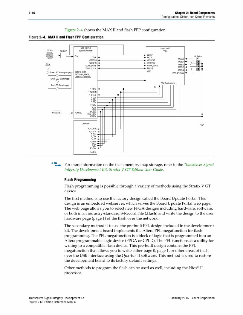
Figure 2–4 shows the MAX II and flash FPP configuration.
f For more information on the flash memory map storage, refer to the Transceiver Signal Integrity Development Kit, Stratix V GT Edition User Guide.
Flash Programming
Flash programming is possible through a variety of methods using the Stratix V GT device.
The first method is to use the factory design called the Board Update Portal. This design is an embedded webserver, which serves the Board Update Portal web page. The web page allows you to select new FPGA designs including hardware, software, or both in an industry-standard S-Record File (.flash) and write the design to the user hardware page (page 1) of the flash over the network.
The secondary method is to use the pre-built PFL design included in the development kit. The development board implements the Altera PFL megafunction for flash programming. The PFL megafunction is a block of logic that is programmed into an Altera programmable logic device (FPGA or CPLD). The PFL functions as a utility for writing to a compatible flash device. This pre-built design contains the PFL megafunction that allows you to write either page 0, page 1, or other areas of flash over the USB interface using the Quartus II software. This method is used to restore the development board to its factory default settings.
Other methods to program the flash can be used as well, including the Nios® II processor.
Figure 2–4. MAX II and Flash FPP Configuration
MAX II CPLDSystem Controller
CONF_D[15:0]
DCLK DCLKCLKxP
F_AD[26:1]
F_D[15:0]
D[15:0]
nSTATUSnCONFIGCONF_DONE
MSEL0MSEL1MSEL2MSEL3
nCE
CFI Flash
Green LED (Factory Image)
Green LED (User Image)
Red LED (Error Image)
F_CEnF_OEn
F_WEn
DEV_CLRn
nCONFIGCONF_DONE
FSM Bus Interface
PGMSELPGM [2:0]
CLKBUF
nSTATUS
CLK
ADVn
CONFIG_ERR,FACTORY_IMAGE,USER_IMAGE LEDs
2.5 V
F_CLK
F_RSTn
RESETn
RY/BYnWPn
RY/BYnWPn
50 MHz
MSEL4MAX_BYPASS
DIP Switch(S7)
RESETn
F_AD[26:1]F_D[15:0]
F_CEnF_OEn
F_WEnADVn
F_CLK
Stratix V GTFPGA
Transceiver Signal Integrity Development Kit January 2016 Altera CorporationStratix V GT Edition Reference Manual

Chapter 2: Board Components 2–17Configuration, Status, and Setup Elements
f For more information on the Nios II processor, refer to the Nios II Processor page of the Altera website.
FPGA Programming over External USB-BlasterThe JTAG header provides another method for configuring the FPGA (U29) using an external USB-Blaster device with the Quartus II Programmer running on a PC. The external USB-Blaster connects to the board through the JTAG header (J93). The JTAG DIP switch (S7) allows the MAX II CPLD device to be removed from the JTAG chain so that the FPGA is the only device on the JTAG chain.
JTAG HeaderThe JTAG header provides another method for configuring the FPGA using an Altera USB-Blaster dongle with the Quartus II Programmer running on a PC. Figure 2–5 shows the schematic connections for the dedicated JTAG programming header (J93). The program MSEL switch (S7) allows the MAX II CPLD device to be removed from the JTAG chain so that the FPGA is the only device on the JTAG chain.
The MAX II CPLD System Controller must be in the chain to use some of the GUI interfaces. To connect the MAX II CPLD in chain, set pins 6-7 of the program MSEL switch (S7) to 1.
f For more information on the following topics, refer to the respective documents:
■ Board Update Portal and PFL Design, refer to the Transceiver Signal Integrity Development Kit, Stratix V GT Edition User Guide.
■ PFL megafunction, refer to AN 386: Using the Parallel Flash Loader with the Quartus II Software.
Figure 2–5. JTAG Header
Stratix V GT FPGA
External USB-Blaster Header
Remove jumper to excludethe MAX CPLD device
from the JTAG chain.
Jumper
DualAnalogSwitchTDI
TMS
TCK
LAST_TDO
LAST_TDO
S5GT_TDIS5GT_TDO
JTAG_TMS
JTAG_TCK
MAX CPLD
TDI
TDO
TMS
TCK IO_TDI
IO_TDO
IO_TMS
IO_TCK
MAX_OEn
JTAG_TMS
JTAG_TCK
MAX_FPP_TDI MAX_FPP_TDO
MAX II and Flash FPP
95
12
3
JTAGHeader
USB Interface
9
5
1
3
January 2016 Altera Corporation Transceiver Signal Integrity Development KitStratix V GT Edition Reference Manual
2–18 Chapter 2: Board ComponentsConfiguration, Status, and Setup Elements
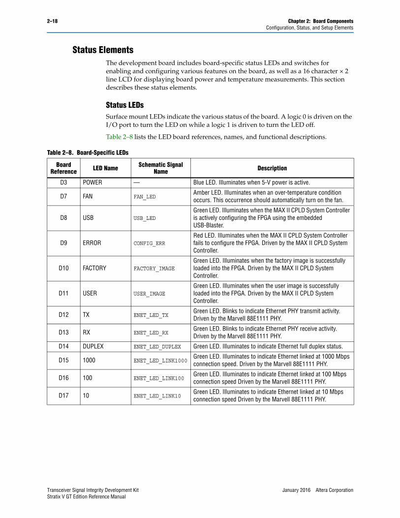
Status ElementsThe development board includes board-specific status LEDs and switches for enabling and configuring various features on the board, as well as a 16 character × 2 line LCD for displaying board power and temperature measurements. This section describes these status elements.
Status LEDsSurface mount LEDs indicate the various status of the board. A logic 0 is driven on the I/O port to turn the LED on while a logic 1 is driven to turn the LED off.
Table 2–8 lists the LED board references, names, and functional descriptions.
Table 2–8. Board-Specific LEDs
Board Reference LED Name Schematic Signal
Name Description
D3 POWER — Blue LED. Illuminates when 5-V power is active.
D7 FAN FAN_LEDAmber LED. Illuminates when an over-temperature condition occurs. This occurrence should automatically turn on the fan.
D8 USB USB_LEDGreen LED. Illuminates when the MAX II CPLD System Controller is actively configuring the FPGA using the embedded USB-Blaster.
D9 ERROR CONFIG_ERRRed LED. Illuminates when the MAX II CPLD System Controller fails to configure the FPGA. Driven by the MAX II CPLD System Controller.
D10 FACTORY FACTORY_IMAGEGreen LED. Illuminates when the factory image is successfully loaded into the FPGA. Driven by the MAX II CPLD System Controller.
D11 USER USER_IMAGEGreen LED. Illuminates when the user image is successfully loaded into the FPGA. Driven by the MAX II CPLD System Controller.
D12 TX ENET_LED_TXGreen LED. Blinks to indicate Ethernet PHY transmit activity. Driven by the Marvell 88E1111 PHY.
D13 RX ENET_LED_RXGreen LED. Blinks to indicate Ethernet PHY receive activity. Driven by the Marvell 88E1111 PHY.
D14 DUPLEX ENET_LED_DUPLEX Green LED. Illuminates to indicate Ethernet full duplex status.
D15 1000 ENET_LED_LINK1000Green LED. Illuminates to indicate Ethernet linked at 1000 Mbps connection speed. Driven by the Marvell 88E1111 PHY.
D16 100 ENET_LED_LINK100Green LED. Illuminates to indicate Ethernet linked at 100 Mbps connection speed Driven by the Marvell 88E1111 PHY.
D17 10 ENET_LED_LINK10Green LED. Illuminates to indicate Ethernet linked at 10 Mbps connection speed Driven by the Marvell 88E1111 PHY.
Transceiver Signal Integrity Development Kit January 2016 Altera CorporationStratix V GT Edition Reference Manual
Chapter 2: Board Components 2–19Configuration, Status, and Setup Elements
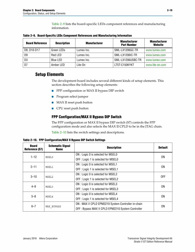
Table 2–9 lists the board-specific LEDs component references and manufacturing information.
Setup ElementsThe development board includes several different kinds of setup elements. This section describes the following setup elements:
■ FPP configuration or MAX II bypass DIP switch
■ Program select jumper
■ MAX II reset push button
■ CPU reset push button
FPP Configuration/MAX II Bypass DIP SwitchThe FPP configuration or MAX II bypass DIP switch (S7) controls the FPP configuration mode and also selects the MAX II CPLD to be in the JTAG chain.
Table 2–10 lists the switch settings and descriptions.
Table 2–9. Board-Specific LEDs Component References and Manufacturing Information
Board Reference Description Manufacturer Manufacturer Part Number
Manufacturer Website
D8, D10-D17 Green LEDs Lumex Inc. SML-LX1206GC-TR www.lumex.com
D9 Red LED Lumex Inc. SML-LX1206IC-TR www.lumex.com
D3 Blue LED Lumex Inc. SML-LX1206USBC-TR www.lumex.com
D7 Amber LED Lite-On LTST-C150KYKT www.lite-on.com
Table 2–10. FPP Configuration/MAX II Bypass DIP Switch Settings
Board Reference (S7)
Schematic Signal Name Description Default
1–12 MSEL0ON : Logic 0 is selected for MSEL0
OFF : Logic 1 is selected for MSEL0ON
2–11 MSEL1ON : Logic 0 is selected for MSEL1
OFF : Logic 1 is selected for MSEL1ON
3–10 MSEL2ON : Logic 0 is selected for MSEL2
OFF : Logic 1 is selected for MSEL2OFF
4–9 MSEL3ON : Logic 0 is selected for MSEL3
OFF : Logic 1 is selected for MSEL3ON
5–8 MSEL4ON : Logic 0 is selected for MSEL4
OFF : Logic 1 is selected for MSEL4ON
6–7 MAX_BYPASSON : MAX II CPLD EPM2210 System Controller in-chain
OFF : Bypass MAX II CPLD EPM2210 System ControllerON
January 2016 Altera Corporation Transceiver Signal Integrity Development KitStratix V GT Edition Reference Manual
2–20 Chapter 2: Board ComponentsConfiguration, Status, and Setup Elements
Table 2–11 lists the DIP switch component reference and manufacturing information.
Program Select JumperThe program select jumper, PGMSEL (J28) is an input to the MAX II CPLD System Controller. After a power-on or reset configuration, the MAX II CPLD System Controller configures the FPGA to either factory or user image. For information on the jumper settings, refer to “FPGA Programming from Flash Memory” on page 2–15.
Reset Push ButtonThe reset push button, RESETn, is an input to the MAX II CPLD System Controller. This push button is the default logic reset for the CPLD logic.
Table 2–12 lists the MAX II reset push button component reference and manufacturing information.
CPU Reset Push ButtonThe CPU reset push button, CPURSTn, (S6) connects to a regular I/O pin of the FPGA and serves as a reset for the NIOS II when you load the application.
Table 2–13 lists the CPU reset configuration push button component reference and manufacturing information.
Table 2–11. FPP Configuration/MAX II Bypass DIP Switch Component Reference and Manufacturing Information
Board Reference Description Manufacturer Manufacturer Part Number Manufacturer Website
S7 Six-Position slide DIP switch Grayhill 97C06RT www.grayhill.com
Table 2–12. MAX II Reset Push Button Component Reference and Manufacturing Information
Board Reference Description Manufacturer Manufacturer Part Number
Manufacturer Website
S5 Push Button Panasonic Corporation EVQPAC07K www.panasonic.com
Table 2–13. CPU Reset Configuration Push Button Component Reference and Manufacturing Information
Board Reference Description Manufacturer Manufacturer Part Number
Manufacturer Website
S6 Push Button Panasonic Corporation EVQPAC07K www.panasonic.com
Transceiver Signal Integrity Development Kit January 2016 Altera CorporationStratix V GT Edition Reference Manual
Chapter 2: Board Components 2–21Clock Circuitry
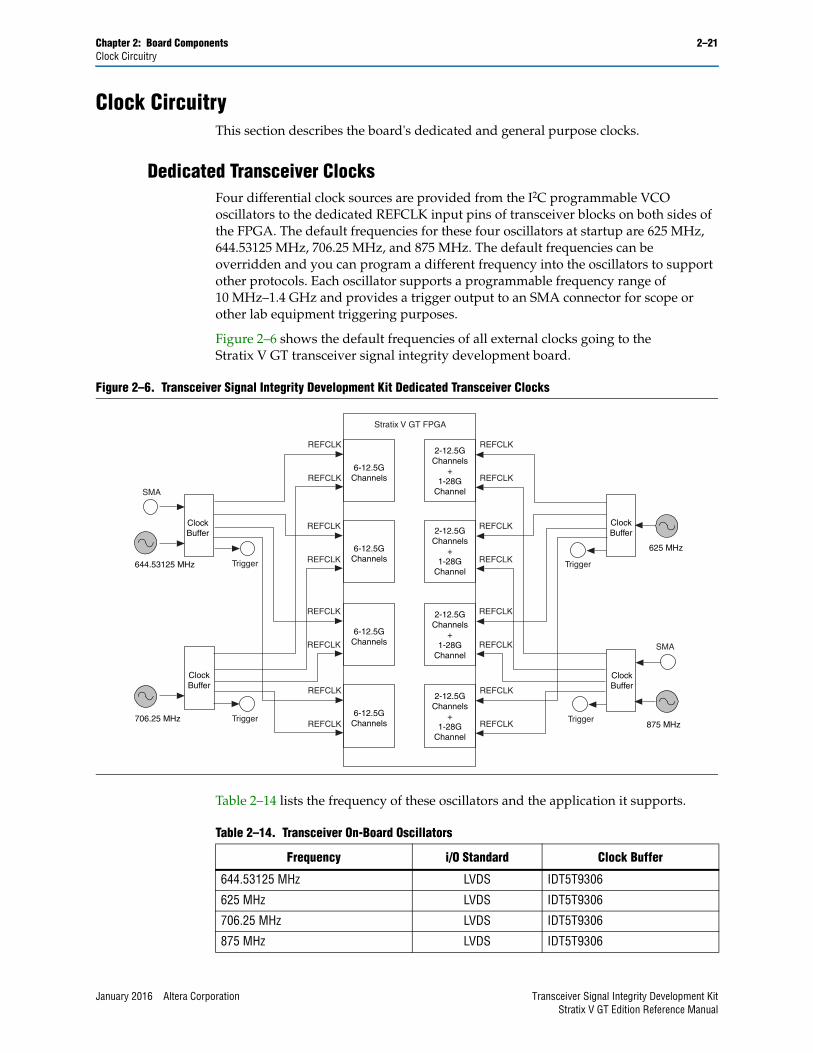
Clock CircuitryThis section describes the board's dedicated and general purpose clocks.
Dedicated Transceiver ClocksFour differential clock sources are provided from the I2C programmable VCO oscillators to the dedicated REFCLK input pins of transceiver blocks on both sides of the FPGA. The default frequencies for these four oscillators at startup are 625 MHz, 644.53125 MHz, 706.25 MHz, and 875 MHz. The default frequencies can be overridden and you can program a different frequency into the oscillators to support other protocols. Each oscillator supports a programmable frequency range of 10 MHz–1.4 GHz and provides a trigger output to an SMA connector for scope or other lab equipment triggering purposes.
Figure 2–6 shows the default frequencies of all external clocks going to the Stratix V GT transceiver signal integrity development board.
Table 2–14 lists the frequency of these oscillators and the application it supports.
Figure 2–6. Transceiver Signal Integrity Development Kit Dedicated Transceiver Clocks
6-12.5GChannels
ClockBuffer
6-12.5GChannels
6-12.5GChannels
6-12.5GChannels
2-12.5GChannels
+1-28G
Channel
2-12.5GChannels
+1-28G
Channel
2-12.5GChannels
+1-28G
Channel
2-12.5GChannels
+1-28G
Channel
644.53125 MHz Trigger
Trigger
ClockBuffer
706.25 MHz Trigger
ClockBuffer
625 MHz
Trigger
SMA
REFCLK
Stratix V GT FPGA
REFCLK
REFCLK
REFCLK
REFCLK
REFCLK
REFCLK
REFCLK
REFCLK
REFCLK
REFCLK
REFCLK
REFCLK
REFCLK
REFCLK
REFCLK
ClockBuffer
875 MHz
SMA
Table 2–14. Transceiver On-Board Oscillators
Frequency i/O Standard Clock Buffer
644.53125 MHz LVDS IDT5T9306
625 MHz LVDS IDT5T9306
706.25 MHz LVDS IDT5T9306
875 MHz LVDS IDT5T9306
January 2016 Altera Corporation Transceiver Signal Integrity Development KitStratix V GT Edition Reference Manual
2–22 Chapter 2: Board ComponentsClock Circuitry
In addition to the four oscillators, each side has a dedicated differential REFCLK input from a pair of SMA connectors to allow an external clock source.
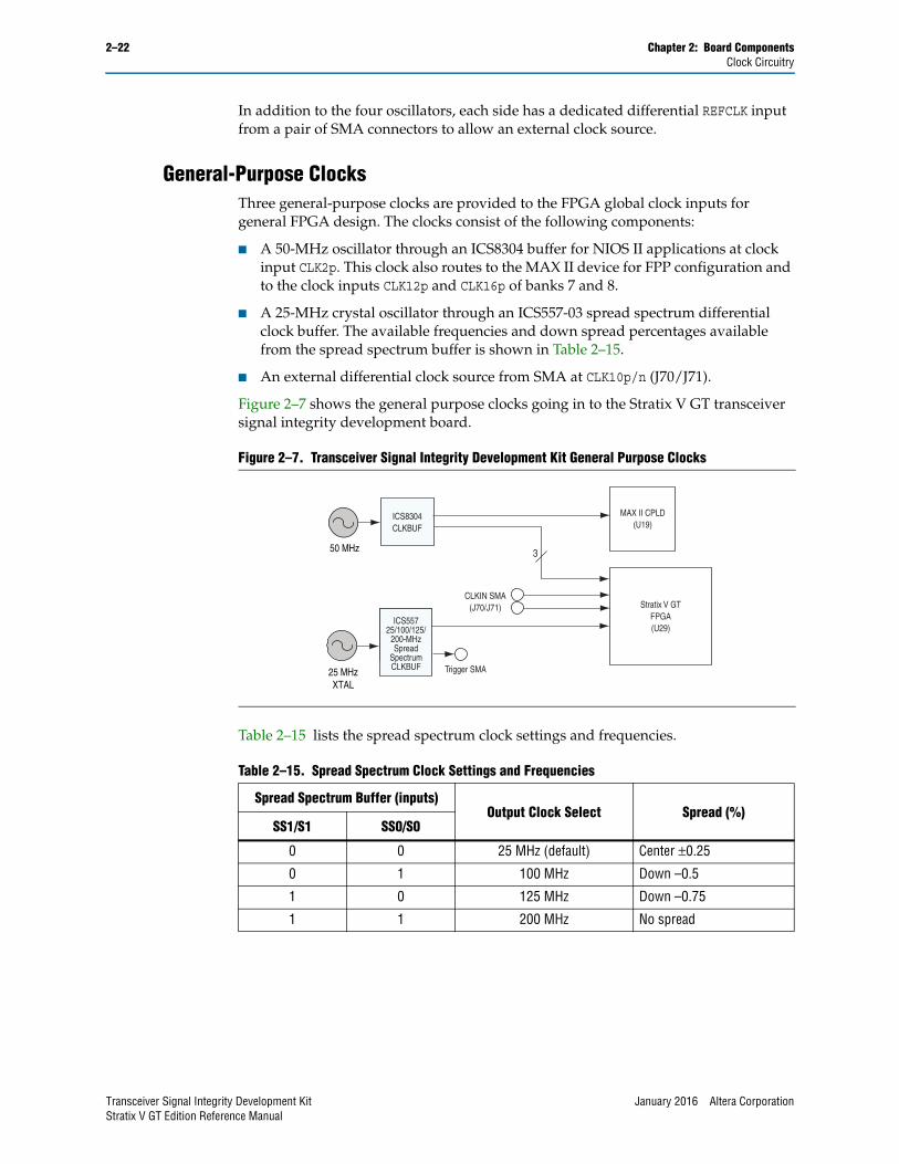
General-Purpose ClocksThree general-purpose clocks are provided to the FPGA global clock inputs for general FPGA design. The clocks consist of the following components:
■ A 50-MHz oscillator through an ICS8304 buffer for NIOS II applications at clock input CLK2p. This clock also routes to the MAX II device for FPP configuration and to the clock inputs CLK12p and CLK16p of banks 7 and 8.
■ A 25-MHz crystal oscillator through an ICS557-03 spread spectrum differential clock buffer. The available frequencies and down spread percentages available from the spread spectrum buffer is shown in Table 2–15.
■ An external differential clock source from SMA at CLK10p/n (J70/J71).
Figure 2–7 shows the general purpose clocks going in to the Stratix V GT transceiver signal integrity development board.
Table 2–15 lists the spread spectrum clock settings and frequencies.
Figure 2–7. Transceiver Signal Integrity Development Kit General Purpose Clocks
Table 2–15. Spread Spectrum Clock Settings and Frequencies
Spread Spectrum Buffer (inputs)Output Clock Select Spread (%)
SS1/S1 SS0/S0
0 0 25 MHz (default) Center ±0.25
0 1 100 MHz Down –0.5
1 0 125 MHz Down –0.75
1 1 200 MHz No spread
ICS8304CLKBUF
MAX II CPLD(U19)
CLKIN SMA(J70/J71)
Trigger SMA
ICS55725/100/125/
200-MHzSpread
SpectrumCLKBUF
Stratix V GTFPGA(U29)
50 MHz
25 MHzXTAL
3
Transceiver Signal Integrity Development Kit January 2016 Altera CorporationStratix V GT Edition Reference Manual
Chapter 2: Board Components 2–23Transceiver Channels
Embedded USB-Blaster ClocksA separate 6-MHz crystal and 24-MHz oscillator are dedicated for the embedded USB-Blaster circuitry. The 6-MHz oscillator is to clock the FTDI FT245 USB PHY device while the 24-MHz oscillator is to clock the MAX II CPLD device. Refer to “FPGA Programming over Embedded USB-Blaster” on page 2–14 for the embedded USB-Blaster implementation.
Table 2–16 lists the crystal oscillators component references and manufacturing information.
Transceiver ChannelsThe transceiver signal integrity development board dedicates 31 (out of 32) 12.5-Gbps transceiver channels from both the left and right sides of the device to various backplane connectors—SFP+ and XFP cages, and SMA connectors. One 12.5-Gbps channel on the 28 Gbps side of the device is a dedicated CMU clock input from the SMA connectors. For the Stratix V GT device, the four 25.78-Gbps ATT channels connects to the MMPX connectors.
Table 2–16. Crystal Oscillator Component References and Manufacturing Information
Board Reference Description Manufacturer Manufacturer
Part Number Manufacturer Website
X1 Crystal oscillator, 6.0 MHz, SMD ESC Inc. ECSX-60-32-5P-TR www.ecsxtal.com
Y1 Crystal oscillator, CMOS, 2.5 V, 24.000 MHz, SMT, ±50ppm Epson SG-310SDF 24.0000M-
B3www.epsontoyocom.co.jp/english/index.html
January 2016 Altera Corporation Transceiver Signal Integrity Development KitStratix V GT Edition Reference Manual
2–24 Chapter 2: Board ComponentsTransceiver Channels
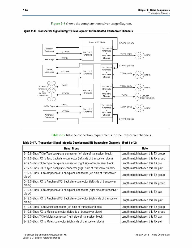
Figure 2–8 shows the complete transceiver usage diagram.
Table 2–17 lists the connection requirements for the transceiver channels.
Figure 2–8. Transceiver Signal Integrity Development Kit Dedicated Transceiver Channels
Six 12.5 GChannels
Two 12.5 GChannels
+One 28 GChannel
Six 12.5 GChannels
Two 12.5 GChannels
+One 28 GChannel
Six 12.5 GChannels
Two 12.5 GChannels
+One 28 GChannel
Six 12.5 GChannels
Two 12.5 GChannels
+One 28 GChannel
Tyco BPConnector
MolexConnector
XFP Cage
AmphenolConnector
SFP+ Cage
5-TX/RX
Stratix V GT FPGA
2-TX/RX (12.5G)
2-TX/RX (12.5G)
2-TX/RX (12.5G)
6-TX/RX
7-TX/RXChannels
to28 SMA
Connectors
TX/RX
TX/RX
MMPX
MMPX
MMPX
MMPX
1 CMURXClock from SMA
TX/RX
TX/RX
5-TX/RX
5-TX/RX
TX/RX (28G)
TX/RX (28G)
TX/RX (28G)
TX/RX (28G)
Table 2–17. Transceiver Signal Integrity Development Kit Transceiver Channels (Part 1 of 2)
Signal Group Note
5-12.5-Gbps TX to Tyco backplane connector (left side of transceiver block) Length match between this TX group
5-12.5-Gbps RX to Tyco backplane connector (left side of transceiver block) Length match between this RX group
2-12.5-Gbps TX to Tyco backplane connector (right side of transceiver block) Length match between this TX pair
2-12.5-Gbps RX to Tyco backplane connector (right side of transceiver block) Length match between this RX pair
5-12.5-Gbps TX to Amphenol/FCI backplane connector (left side of transceiver block) Length match between this TX group
5-12.5-Gbps RX to Amphenol/FCI backplane connector (left side of transceiver block) Length match between this RX group
2-12.5-Gbps TX to Amphenol/FCI backplane connector (right side of transceiver block) Length match between this TX pair
2-12.5-Gbps RX to Amphenol/FCI backplane connector (right side of transceiver block) Length match between this RX pair
5-12.5-Gbps TX to Molex connector (left side of transceiver block) Length match between this TX group
5-12.5-Gbps RX to Molex connector (left side of transceiver block) Length match between this RX group
2-12.5-Gbps TX to Molex connector (right side of transceiver block) Length match between this TX pair
2-12.5-Gbps RX to Molex connector (right side of transceiver block) Length match between this RX pair
Transceiver Signal Integrity Development Kit January 2016 Altera CorporationStratix V GT Edition Reference Manual

Chapter 2: Board Components 2–25Backplane Connectors
Backplane ConnectorsThe development board supports three different types of 10Gbase-KR reference backplanes by directly mating with the backplanes made from Tyco, Amphenol, and Molex manufacturers.
Table 2–18 lists the Amphenol backplane connector pin assignments.
7-12.5-Gbps TX to SMAs (left side of transceiver block) Length match between this TX group
7-12.5-Gbps RX to SMAs—can be used as CMUclk inputs (left side of transceiver block) Length match between this RX group
4-25.78-Gbps TX to MMPX connector (right side of transceiver block) Length match between this TX group
4-25.78-Gbps RX to MMPX connector (right side of transceiver block) Length match between this RX group
1-12.5-Gbps TX/RX to SFP+ cage (left side of transceiver block) No matching between TX/RX pairs
1-12.5-Gbps TX/RX to XFP cage (left side of transceiver block) No matching between TX/RX pairs
1-12.5-Gbps RX channel used as CMUclk input from SMA (right side of transceiver block) Match P/N of RX input
Table 2–17. Transceiver Signal Integrity Development Kit Transceiver Channels (Part 2 of 2)
Signal Group Note
Table 2–18. Amphenol Backplane Connector Pin Assignments, Signal Names and Functions (Part 1 of 2)
Board Reference (J32) Schematic Signal Name I/O Standard Stratix V GT Device
Pin Number Description
G5 GXB_TXLN_19 1.4-V PCML K35 GXB transmit
H5 GXB_TXLP_19 1.4-V PCML K34 GXB transmit
E5 GXB_TXLN_20 1.4-V PCML J37 GXB transmit
F5 GXB_TXLP_20 1.4-V PCML J36 GXB transmit
E4 GXB_TXLN_21 1.4-V PCML G37 GXB transmit
F4 GXB_TXLP_21 1.4-V PCML G36 GXB transmit
C5 GXB_TXLN_22 1.4-V PCML E37 GXB transmit
D5 GXB_TXLP_22 1.4-V PCML E36 GXB transmit
C4 GXB_TXLN_23 1.4-V PCML C37 GXB transmit
D4 GXB_TXLP_23 1.4-V PCML C36 GXB transmit
E6 GXB_TXRN_18 1.4-V PCML M5 GXB transmit
F6 GXB_TXRP_18 1.4-V PCML M6 GXB transmit
C6 GXB_TXRN_23 1.4-V PCML C3 GXB transmit
D6 GXB_TXRP_23 1.4-V PCML C4 GXB transmit
C1 GXBRXLN_19 1.4-V PCML K39 GXB receive
D1 GXBRXLP_19 1.4-V PCML K38 GXB receive
C2 GXBRXLN_20 1.4-V PCML H39 GXB receive
D2 GXBRXLP_20 1.4-V PCML H38 GXB receive
E1 GXBRXLN_21 1.4-V PCML F39 GXB receive
F1 GXBRXLP_21 1.4-V PCML F38 GXB receive
E2 GXBRXLN_22 1.4-V PCML D39 GXB receive
January 2016 Altera Corporation Transceiver Signal Integrity Development KitStratix V GT Edition Reference Manual
2–26 Chapter 2: Board ComponentsBackplane Connectors
Table 2–19 lists the Tyco backplane connector pin assignments.
F2 GXBRXLP_22 1.4-V PCML D38 GXB receive
G2 GXBRXLN_23 1.4-V PCML B39 GXB receive
H2 GXBRXLP_23 1.4-V PCML B38 GXB receive
E3 GXBRXRN_18 1.4-V PCML L3 GXB receive
F3 GXBRXRP_18 1.4-V PCML L4 GXB receive
C3 GXBRXRN_23 1.4-V PCML B1 GXB receive
D3 GXBRXRP_23 1.4-V PCML B2 GXB receive
Table 2–18. Amphenol Backplane Connector Pin Assignments, Signal Names and Functions (Part 2 of 2)
Board Reference (J32) Schematic Signal Name I/O Standard Stratix V GT Device
Pin Number Description
Table 2–19. Tyco Backplane Connector Pin Assignments, Signal Names and Functions (Part 1 of 2)
Board Reference (J33) Schematic Signal Name I/O Standard Stratix V GT Device
Pin Number Description
F11 GXB_TXLN_0 1.4-V PCML AU37 GXB transmit
G11 GXB_TXLN_1 1.4-V PCML AR37 GXB transmit
H11 GXB_TXLN_2 1.4-V PCML AN37 GXB transmit
F14 GXB_TXLN_3 1.4-V PCML AL37 GXB transmit
G14 GXB_TXLN_4 1.4-V PCML AK35 GXB transmit
F12 GXB_TXLP_0 1.4-V PCML AU36 GXB transmit
G12 GXB_TXLP_1 1.4-V PCML AR36 GXB transmit
H12 GXB_TXLP_2 1.4-V PCML AN36 GXB transmit
F15 GXB_TXLP_3 1.4-V PCML AL36 GXB transmit
G15 GXB_TXLP_4 1.4-V PCML AK34 GXB transmit
F18 GXB_TXRN_0 1.4-V PCML AU3 GXB transmit
G18 GXB_TXRN_5 1.4-V PCML AH5 GXB transmit
F17 GXB_TXRP_0 1.4-V PCML AU4 GXB transmit
G17 GXB_TXRP_5 1.4-V PCML AH6 GXB transmit
B2 GXBRXLN_0 1.4-V PCML AV39 GXB receive
C2 GXBRXLN_1 1.4-V PCML AT39 GXB receive
B5 GXBRXLN_2 1.4-V PCML AP39 GXB receive
A5 GXBRXLN_3 1.4-V PCML AM39 GXB receive
A2 GXBRXLN_4 1.4-V PCML AJ37 GXB receive
B3 GXBRXLP_0 1.4-V PCML AV38 GXB receive
C3 GXBRXLP_1 1.4-V PCML AT38 GXB receive
B6 GXBRXLP_2 1.4-V PCML AP38 GXB receive
A6 GXBRXLP_3 1.4-V PCML AM38 GXB receive
A3 GXBRXLP_4 1.4-V PCML AJ36 GXB receive
A9 GXBRXRN_0 1.4-V PCML AV1 GXB receive
B9 GXBRXRN_5 1.4-V PCML AJ3 GXB receive
Transceiver Signal Integrity Development Kit January 2016 Altera CorporationStratix V GT Edition Reference Manual
Chapter 2: Board Components 2–27Backplane Connectors
Table 2–20 lists the Molex backplane connector pin assignments.
A8 GXBRXRP_0 1.4-V PCML AV2 GXB receive
B8 GXBRXRP_5 1.4-V PCML AJ4 GXB receive
Table 2–19. Tyco Backplane Connector Pin Assignments, Signal Names and Functions (Part 2 of 2)
Board Reference (J33) Schematic Signal Name I/O Standard Stratix V GT Device
Pin Number Description
Table 2–20. Molex Backplane Connector Pin Assignments, Signal Names and Functions
Board Reference (J34) Schematic Signal Name I/O Standard Stratix V GT Device
Pin Number Description
E9 GXB_TXLN_6 1.4-V PCML AG37 GXB transmit
H9 GXB_TXLN_7 1.4-V PCML AF35 GXB transmit
B9 GXB_TXLN_8 1.4-V PCML AD35 GXB transmit
D10 GXB_TXLN_9 1.4-V PCML AC37 GXB transmit
G10 GXB_TXLN_10 1.4-V PCML AB35 GXB transmit
F9 GXB_TXLP_6 1.4-V PCML AG36 GXB transmit
J9 GXB_TXLP_7 1.4-V PCML AF34 GXB transmit
C9 GXB_TXLP_8 1.4-V PCML AD34 GXB transmit
E10 GXB_TXLP_9 1.4-V PCML AC36 GXB transmit
H10 GXB_TXLP_10 1.4-V PCML AB34 GXB transmit
D8 GXB_TXRN_6 1.4-V PCML AG3 GXB transmit
G8 GXB_TXRN_11 1.4-V PCML Y5 GXB transmit
E8 GXB_TXRP_6 1.4-V PCML AG4 GXB transmit
H8 GXB_TXRP_11 1.4-V PCML Y6 GXB transmit
H3 GXBRXLN_6 1.4-V PCML AH39 GXB receive
K2 GXBRXLN_7 1.4-V PCML AE37 GXB receive
G4 GXBRXLN_8 1.4-V PCML AF39 GXB receive
L3 GXBRXLN_9 1.4-V PCML AD39 GXB receive
K4 GXBRXLN_10 1.4-V PCML AB39 GXB receive
J3 GXBRXLP_6 1.4-V PCML AH38 GXB receive
L2 GXBRXLP_7 1.4-V PCML AE36 GXB receive
H4 GXBRXLP_8 1.4-V PCML AF38 GXB receive
M3 GXBRXLP_9 1.4-V PCML AD38 GXB receive
L4 GXBRXLP_10 1.4-V PCML AB38 GXB receive
E3 GXBRXRN_6 1.4-V PCML AH1 GXB receive
G2 GXBRXRN_11 1.4-V PCML AA3 GXB receive
F3 GXBRXRP_6 1.4-V PCML AH2 GXB receive
H2 GXBRXRP_11 1.4-V PCML AA4 GXB receive
January 2016 Altera Corporation Transceiver Signal Integrity Development KitStratix V GT Edition Reference Manual
2–28 Chapter 2: Board ComponentsGeneral User Input/Output
Table 2–21 lists the backplane connector component reference and the manufacturing information.
General User Input/OutputThis section describes the user I/O interface to the FPGA. This section describes the following I/O elements:
■ User-defined push buttons
■ User-defined DIP switch
■ User-defined LEDs
■ Character LCD
User-Defined Push ButtonsThe development board includes four user-defined push buttons that allow you to interact with the Stratix V GT device. When you press and hold down the push button, the device pin is set to logic 0; when you release the push button, the device pin is set to logic 1. There is no board-specific function for these general user push buttons.
Table 2–22 lists the user-defined push button schematic signal names and their corresponding Stratix V GT device pin numbers.
Table 2–23 lists the user-defined push button component reference and the manufacturing information.
Table 2–21. User-Defined Push Button Component Reference and Manufacturing Information
Board Reference Description Manufacturer Manufacturer
Part NumberManufacturer
Website
J32 Connector, 4-pair, 6 position, Amphenol Xcede Amphenol AX400-00682 www.amphenol.com
J33 Connector, 8-pair, 6-columns, receptacle, Tyco Strada Tyco Electronics 2149323-1 www.te.com
J34 Connector, 4-pair, receptacle, Molex Impact Molex 76160-5020 www.molex.com
Table 2–22. User-Defined Push Button Schematic Signal Names and Functions
Board Reference Schematic Signal Name I/O Standard Stratix V GT Device Pin Number
S1 USER_PB0 2.5-V H29
S2 USER_PB1 2.5-V G28
S3 USER_PB2 2.5-V K27
S4 USER_PB3 2.5-V J27
Table 2–23. User-Defined Push Button Component Reference and Manufacturing Information
Board Reference Description Manufacturer Manufacturer Part Number Manufacturer Website
S1–S4 Push button Panasonic Corporation EVQPAC07K www.panasonic.com
Transceiver Signal Integrity Development Kit January 2016 Altera CorporationStratix V GT Edition Reference Manual

Chapter 2: Board Components 2–29General User Input/Output
User-Defined DIP SwitchBoard reference SW4 is a 8-pin DIP switch. The switches are user-defined, and are provides additional FPGA input control. When the switch is in the OPEN or ON position, a logic 1 is selected. When the switch is in the CLOSED or OFF position, a logic 0 is selected. There is no board-specific function for these switches.
Table 2–24 lists the user-defined DIP switch schematic signal names and their corresponding Stratix V GT pin numbers.
Table 2–25 lists the user-defined DIP switch component reference and the manufacturing information.
User-Defined LEDsThe development board includes eight user-defined LEDs. Board references D18 through D25 are user LEDs that allow status and debugging signals to be driven to the LEDs from the designs loaded into the Stratix V GT device. The LEDs illuminate when a logic 0 is driven, and turns off when a logic 1 is driven. There is no board-specific function for these LEDs.
Table 2–26 lists the user-defined LED schematic signal names and their corresponding Stratix V GT pin numbers.
Table 2–24. User-Defined DIP Switch Schematic Signal Names and Functions
Board Reference (SW4) Schematic Signal Name I/O Standard Stratix V GT Device Pin Number
1 S5_UNLOCK 2.5-V—
(Connects to USB MAX II pin B6)
2 USER_DIP6 2.5-V H34
3 USER_DIP5 2.5-V F33
4 USER_DIP4 2.5-V G33
5 USER_DIP3 2.5-V H32
6 USER_DIP2 2.5-V D34
7 USER_DIP1 2.5-V E34
8 USER_DIP0 2.5-V D33
Table 2–25. User-Defined DIP Switch Component Reference and Manufacturing Information
Board Reference Description Manufacturer Manufacturer Part Number Manufacturer Website
SW4 Eight-Position DIP switch Grayhill 76SB08ST www.grayhill.com
Table 2–26. User-Defined LED Schematic Signal Names and Functions (Part 1 of 2)
Board Reference Schematic Signal Name I/O Standard Stratix V GT Device Pin Number
D18 USER_LED_0 2.5-V B32
D19 USER_LED_1 2.5-V A32
D20 USER_LED_2 2.5-V B34
D21 USER_LED_3 2.5-V A34
January 2016 Altera Corporation Transceiver Signal Integrity Development KitStratix V GT Edition Reference Manual
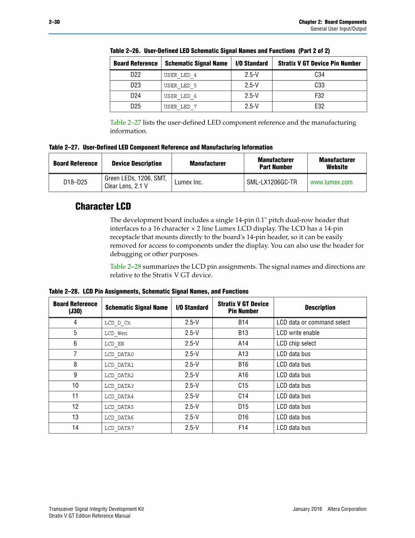
2–30 Chapter 2: Board ComponentsGeneral User Input/Output
Table 2–27 lists the user-defined LED component reference and the manufacturing information.
Character LCD The development board includes a single 14-pin 0.1" pitch dual-row header that interfaces to a 16 character × 2 line Lumex LCD display. The LCD has a 14-pin receptacle that mounts directly to the board's 14-pin header, so it can be easily removed for access to components under the display. You can also use the header for debugging or other purposes.
Table 2–28 summarizes the LCD pin assignments. The signal names and directions are relative to the Stratix V GT device.
D22 USER_LED_4 2.5-V C34
D23 USER_LED_5 2.5-V C33
D24 USER_LED_6 2.5-V F32
D25 USER_LED_7 2.5-V E32
Table 2–26. User-Defined LED Schematic Signal Names and Functions (Part 2 of 2)
Board Reference Schematic Signal Name I/O Standard Stratix V GT Device Pin Number
Table 2–27. User-Defined LED Component Reference and Manufacturing Information
Board Reference Device Description Manufacturer Manufacturer Part Number
Manufacturer Website
D18–D25 Green LEDs, 1206, SMT, Clear Lens, 2.1 V Lumex Inc. SML-LX1206GC-TR www.lumex.com
Table 2–28. LCD Pin Assignments, Schematic Signal Names, and Functions
Board Reference (J30) Schematic Signal Name I/O Standard Stratix V GT Device
Pin Number Description
4 LCD_D_Cn 2.5-V B14 LCD data or command select
5 LCD_Wen 2.5-V B13 LCD write enable
6 LCD_EN 2.5-V A14 LCD chip select
7 LCD_DATA0 2.5-V A13 LCD data bus
8 LCD_DATA1 2.5-V B16 LCD data bus
9 LCD_DATA2 2.5-V A16 LCD data bus
10 LCD_DATA3 2.5-V C15 LCD data bus
11 LCD_DATA4 2.5-V C14 LCD data bus
12 LCD_DATA5 2.5-V D15 LCD data bus
13 LCD_DATA6 2.5-V D16 LCD data bus
14 LCD_DATA7 2.5-V F14 LCD data bus
Transceiver Signal Integrity Development Kit January 2016 Altera CorporationStratix V GT Edition Reference Manual
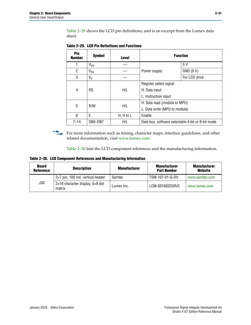
Chapter 2: Board Components 2–31General User Input/Output
Table 2–29 shows the LCD pin definitions, and is an excerpt from the Lumex data sheet.
f For more information such as timing, character maps, interface guidelines, and other related documentation, visit www.lumex.com.
Table 2–30 lists the LCD component references and the manufacturing information.
Table 2–29. LCD Pin Definitions and Functions
Pin Number Symbol Level Function
1 VDD —
Power supply
5 V
2 VSS — GND (0 V)
3 V0 — For LCD drive
4 RS H/L
Register select signal
H: Data input
L: Instruction input
5 R/W H/LH: Data read (module to MPU)
L: Data write (MPU to module)
6 E H, H to L Enable
7–14 DB0–DB7 H/L Data bus, software selectable 4-bit or 8-bit mode
Table 2–30. LCD Component References and Manufacturing Information
Board Reference Description Manufacturer Manufacturer
Part NumberManufacturer
Website
J302×7 pin, 100 mil, vertical header Samtec TSM-107-01-G-DV www.samtec.com
2×16 character display, 5×8 dot matrix Lumex Inc. LCM-S01602DSR/C www.lumex.com
January 2016 Altera Corporation Transceiver Signal Integrity Development KitStratix V GT Edition Reference Manual

2–32 Chapter 2: Board ComponentsComponents and Interfaces
Components and InterfacesThis section describes the development board's communication ports and interface cards relative to the Stratix V GT device. The development board supports the following components and interfaces:
■ 10/100/1000 Ethernet
■ Transceiver interfaces
■ XFP interface
■ Small Form-Factor Pluggable (SFP+) interface
10/100/1000 EthernetThe development board supports a 10/100/1000 BASE-T Ethernet connection using a Marvell 88E1111 PHY device and the Altera Triple-Speed Ethernet MegaCore MAC function. The device is an auto-negotiating Ethernet PHY with an SGMII interface to the FPGA. The Stratix V GT device can communicate with the LVDS interfaces at up to 1.25 Gbps. The MAC function must be provided in the FPGA for typical networking applications. The Marvell 88E1111 PHY uses 2.5-V and 1.2-V power rails and requires a 25-MHz reference clock driven from a dedicated oscillator. It interfaces to an RJ-45 with internal magnetics that can be used for driving copper lines with Ethernet traffic.
Figure 2–9 shows the SGMII interface between the FPGA (MAC) and Marvell 88E1111 PHY.
Table 2–31 lists the Ethernet PHY interface pin assignments.
Figure 2–9. SGMII Interface between FPGA (MAC) and Marvell 88E1111 PHY
MAC 88E1111Device
Transformer RJ45
SGMII Interface
S_IN ±
S_OUT ± CAT 5 UTP:- 10BASE-T- 100BASE-TX- 1000BASE-T
Table 2–31. Ethernet PHY Pin Assignments, Signal Names and Functions (Part 1 of 2)
Board Reference (U22) Schematic Signal Name I/O Standard Stratix V GT
Device Pin Number Description
23 ENET_INTN 2.5-V AL14 Management bus Interrupt
70 ENET_LED_DUPLEX 2.5-V — Duplex LED
76 ENET_LED_LINK10 2.5-V — 10-Mb link LED
74 ENET_LED_LINK100 2.5-V — 100-Mb link LED
73 ENET_LED_LINK1000 2.5-V — 1000-Mb link LED
Transceiver Signal Integrity Development Kit January 2016 Altera CorporationStratix V GT Edition Reference Manual
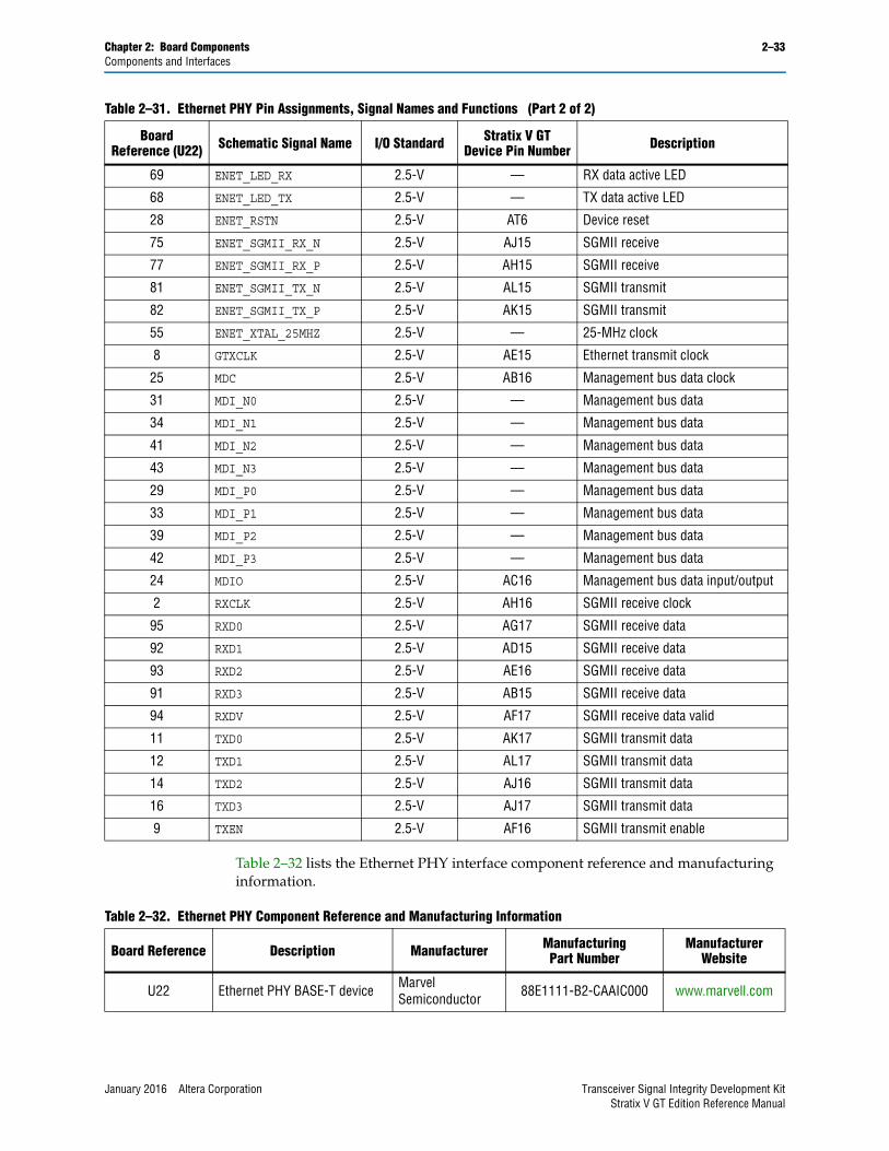
Chapter 2: Board Components 2–33Components and Interfaces
Table 2–32 lists the Ethernet PHY interface component reference and manufacturing information.
69 ENET_LED_RX 2.5-V — RX data active LED
68 ENET_LED_TX 2.5-V — TX data active LED
28 ENET_RSTN 2.5-V AT6 Device reset
75 ENET_SGMII_RX_N 2.5-V AJ15 SGMII receive
77 ENET_SGMII_RX_P 2.5-V AH15 SGMII receive
81 ENET_SGMII_TX_N 2.5-V AL15 SGMII transmit
82 ENET_SGMII_TX_P 2.5-V AK15 SGMII transmit
55 ENET_XTAL_25MHZ 2.5-V — 25-MHz clock
8 GTXCLK 2.5-V AE15 Ethernet transmit clock
25 MDC 2.5-V AB16 Management bus data clock
31 MDI_N0 2.5-V — Management bus data
34 MDI_N1 2.5-V — Management bus data
41 MDI_N2 2.5-V — Management bus data
43 MDI_N3 2.5-V — Management bus data
29 MDI_P0 2.5-V — Management bus data
33 MDI_P1 2.5-V — Management bus data
39 MDI_P2 2.5-V — Management bus data
42 MDI_P3 2.5-V — Management bus data
24 MDIO 2.5-V AC16 Management bus data input/output
2 RXCLK 2.5-V AH16 SGMII receive clock
95 RXD0 2.5-V AG17 SGMII receive data
92 RXD1 2.5-V AD15 SGMII receive data
93 RXD2 2.5-V AE16 SGMII receive data
91 RXD3 2.5-V AB15 SGMII receive data
94 RXDV 2.5-V AF17 SGMII receive data valid
11 TXD0 2.5-V AK17 SGMII transmit data
12 TXD1 2.5-V AL17 SGMII transmit data
14 TXD2 2.5-V AJ16 SGMII transmit data
16 TXD3 2.5-V AJ17 SGMII transmit data
9 TXEN 2.5-V AF16 SGMII transmit enable
Table 2–31. Ethernet PHY Pin Assignments, Signal Names and Functions (Part 2 of 2)
Board Reference (U22) Schematic Signal Name I/O Standard Stratix V GT
Device Pin Number Description
Table 2–32. Ethernet PHY Component Reference and Manufacturing Information
Board Reference Description Manufacturer ManufacturingPart Number
Manufacturer Website
U22 Ethernet PHY BASE-T device Marvel Semiconductor 88E1111-B2-CAAIC000 www.marvell.com
January 2016 Altera Corporation Transceiver Signal Integrity Development KitStratix V GT Edition Reference Manual

2–34 Chapter 2: Board ComponentsComponents and Interfaces
Transceiver InterfacesThe transceiver signal integrity development board incorporates an XFP and SFP+ transceiver module. Each module has a single duplex channel.
XFP InterfaceTable 2–33 lists the XFP connector cage interface pin assignments.
Table 2–34 lists the XFP interface component reference and manufacturing information.
Table 2–33. XFP Interface Pin Assignments, Signal Names and Functions
Board Reference (U25)
Schematic Signal Name I/O Standard Stratix V GT
Device Pin Number Description
28 GXB_TXLN_5 1.4-V PCML AH35 GXB transmit
29 GXB_TXLP_5 1.4-V PCML AH34 GXB transmit
18 GXB_RXLN_5 1.4-V PCML AK39 GXB receive
16 GXB_RXLP_5 1.4-V PCML AK38 GXB receive
24 REFCLK_XFPN 1.8-V — XFP reference clock
25 REFCLK_XFPP 1.8-V — XFP reference clock
3 XFP_MOD_DESEL 1.8-V AV23 Module deselect
21 XFP_PDOWN_RST 1.8-V AW23 Power down reset
4 XFP_T_INTERRUPT 1.8-V AV22 Interrupt
12 XFP_T_MOD_ABS 1.8-V AW26 Module absent
10 XFP_T_SCL 1.8-V AW25 Two-wire serial interface clock line
11 XFP_T_SDA 1.8-V AV25 Two-wire serial interface data line
5 XFP_TX_DIS 1.8-V AW22 Disables transmitter output
Table 2–34. XFP Interface Component Reference and Manufacturing Information
Board Reference Description Manufacturer Manufacturing
Part NumberManufacturer
Website
U25
XFP 30-pin connector, 30UM gold plating, high speed
Amphenol
Tyco1367500-1
www.amphenol.com
www.te.comXFP cage without light pipe, press fit
Amphenol
Tyco1489951-1
Transceiver Signal Integrity Development Kit January 2016 Altera CorporationStratix V GT Edition Reference Manual

Chapter 2: Board Components 2–35Components and Interfaces
SFP+ InterfaceTable 2–31 lists the pin assignments for the SFP+ interface (SFPA) and their corresponding schematic signal names and Stratix V GT pin numbers.
Table 2–34 lists the SFP+ interface component reference and manufacturing information.
Table 2–35. SFP+ Interface Pin Assignments, Signal Names and Functions
Board Reference (J51) Schematic Signal Name I/O Standard Stratix V GT
Device Pin Number Description
19 GXB_TXLN_18 1.8-V M35 GXB transmit
18 GXB_TXLP_18 1.8-V M34 GXB transmit
12 GXB_RXLN_18 1.8-V L37 GXB receive
13 GXB_RXLP_18 1.8-V L36 GXB receive
8 SFPA_LOS 1.8-V B28 Signal loss indicator
6 SFPA_MOD0_PRSNTN 1.8-V B26 Module present indicator
5 SFPA_MOD1_SCL 1.8-V A26 Two-wire serial interface clock line
4 SFPA_MOD2_SDA 1.8-V B25 Two-wire serial interface data line
7 SFPA_RATESEL0 1.8-V C27 Rate select 0. Controls the SFP+ interface receiver.
9 SFPA_RATESEL1 1.8-V C26 Rate select 1. Controls the SFP+ interface receiver.
3 SFPA_TXDISABLE 1.8-V A28 Turns off and disables the transmitter output
2 SFPA_TXFAULT 1.8-V A25 Transmitter fault
Table 2–36. SFP+ Interface Component Reference and Manufacturing Information
Board Reference Description Manufacturer Manufacturing
Part NumberManufacturer
Website
J51SFP+ connector - Mect family standard SFP right-angle 20-pin SMT Samtec MECT-110-01-M-D-RA1 www.samtec.com
SFP+ cage Molex 74754-0101 www.molex.com
January 2016 Altera Corporation Transceiver Signal Integrity Development KitStratix V GT Edition Reference Manual
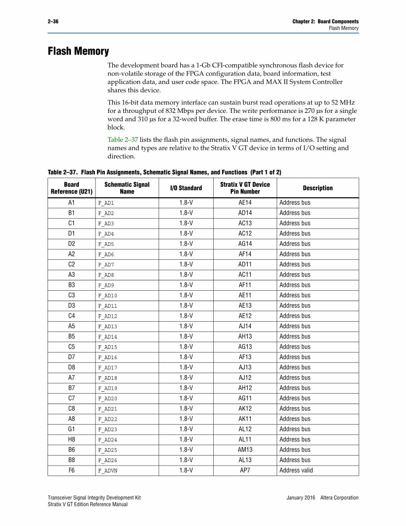
2–36 Chapter 2: Board ComponentsFlash Memory
Flash MemoryThe development board has a 1-Gb CFI-compatible synchronous flash device for non-volatile storage of the FPGA configuration data, board information, test application data, and user code space. The FPGA and MAX II System Controller shares this device.
This 16-bit data memory interface can sustain burst read operations at up to 52 MHz for a throughput of 832 Mbps per device. The write performance is 270 µs for a single word and 310 µs for a 32-word buffer. The erase time is 800 ms for a 128 K parameter block.
Table 2–37 lists the flash pin assignments, signal names, and functions. The signal names and types are relative to the Stratix V GT device in terms of I/O setting and direction.
Table 2–37. Flash Pin Assignments, Schematic Signal Names, and Functions (Part 1 of 2)
Board Reference (U21)
Schematic Signal Name I/O Standard Stratix V GT Device
Pin Number Description
A1 F_AD1 1.8-V AE14 Address bus
B1 F_AD2 1.8-V AD14 Address bus
C1 F_AD3 1.8-V AC13 Address bus
D1 F_AD4 1.8-V AC12 Address bus
D2 F_AD5 1.8-V AG14 Address bus
A2 F_AD6 1.8-V AF14 Address bus
C2 F_AD7 1.8-V AD11 Address bus
A3 F_AD8 1.8-V AC11 Address bus
B3 F_AD9 1.8-V AF11 Address bus
C3 F_AD10 1.8-V AE11 Address bus
D3 F_AD11 1.8-V AE13 Address bus
C4 F_AD12 1.8-V AE12 Address bus
A5 F_AD13 1.8-V AJ14 Address bus
B5 F_AD14 1.8-V AH13 Address bus
C5 F_AD15 1.8-V AG13 Address bus
D7 F_AD16 1.8-V AF13 Address bus
D8 F_AD17 1.8-V AJ13 Address bus
A7 F_AD18 1.8-V AJ12 Address bus
B7 F_AD19 1.8-V AH12 Address bus
C7 F_AD20 1.8-V AG11 Address bus
C8 F_AD21 1.8-V AK12 Address bus
A8 F_AD22 1.8-V AK11 Address bus
G1 F_AD23 1.8-V AL12 Address bus
H8 F_AD24 1.8-V AL11 Address bus
B6 F_AD25 1.8-V AM13 Address bus
B8 F_AD26 1.8-V AL13 Address bus
F6 F_ADVN 1.8-V AP7 Address valid
Transceiver Signal Integrity Development Kit January 2016 Altera CorporationStratix V GT Edition Reference Manual
Chapter 2: Board Components 2–37Power Supply
Table 2–38 lists the flash memory component reference and manufacturing information.
Power SupplyThe development board’s power is provided through a laptop style DC power input. The input voltage must be in the range of 14 V to 20 V. The DC voltage is then stepped down to the various power rails used by the components on the board.
An on-board multi-channel power monitor device (LTC2978) measures both the voltage and current for several specific board rails. This device has the capability to trim voltage outputs ±10%.
F7 F_BSYN 1.8-V AR7 Ready
B4 F_CEN 1.8-V AP9 Chip enable
E6 F_CLK 1.8-V AN6 Clock
F2 F_D0 1.8-V AN11 Data bus
E2 F_D1 1.8-V AM11 Data bus
G3 F_D2 1.8-V AP12 Data bus
E4 F_D3 1.8-V AN12 Data bus
E5 F_D4 1.8-V AN10 Data bus
G5 F_D5 1.8-V AM10 Data bus
G6 F_D6 1.8-V AR11 Data bus
H7 F_D7 1.8-V AR10 Data bus
E1 F_D8 1.8-V AT12 Data bus
E3 F_D9 1.8-V AU13 Data bus
F3 F_D10 1.8-V AU12 Data bus
F4 F_D11 1.8-V AU11 Data bus
F5 F_D12 1.8-V AT11 Data bus
H5 F_D13 1.8-V AW13 Data bus
G7 F_D14 1.8-V AV13 Data bus
E7 F_D15 1.8-V AW11 Data bus
F8 F_OEN 1.8-V AN9 Output enable
D4 F_RSTN 1.8-V AL8 Reset
G8 F_WEN 1.8-V AM8 Write enable
C6 F_WPN 1.8-V AP6 Write protect
Table 2–37. Flash Pin Assignments, Schematic Signal Names, and Functions (Part 2 of 2)
Board Reference (U21)
Schematic Signal Name I/O Standard Stratix V GT Device
Pin Number Description
Table 2–38. Flash Memory Component Reference and Manufacturing Information
Board Reference Description Manufacturer ManufacturingPart Number
Manufacturer Website
U21 1-Gb synchronous flash Micron PC28F00AP30BF www.micron.com
January 2016 Altera Corporation Transceiver Signal Integrity Development KitStratix V GT Edition Reference Manual

2–38 Chapter 2: Board ComponentsPower Supply
Table 2–39 lists the power requirements for each major component on the board.
Table 2–39. Power Requirements
Device Voltage Name Voltage (V) Note
FPGA
S5GX_VCC 0.85
VCC
VCCHIP
VCCHSSI
2p5V 2.5
VCCIO
VCCPD
VCCREF
VCCPGM
VCCBAT
VCC_CLKIN
2p5V_FLTR 2.5 Ferrite fitered from 2p5V, VCCA_PLL, and VCCAUX
1p5V 1.5
VCCPT
VCCH_GXB
VCCD_FPLL
VCCBAT 1.5 BT1 socket
VCCR_GTB (28G channels) 0.85 or 1.0 LDO
VCCT_GTB (28G channels) 0.85 or 1.0 LDO
VCCL_GTB (28G channels) 0.85 or 1.0 LDO
VCCRT_GXB 0.85 or 1.0 Low noise switcher
VCCA_GXB 2.5 or 3 Low noise switcher
VCCH_GXB 1.5 Tied to 1p5V (low noise switcher)
MAX II (for FPP configuration) 2p5V 2.5 —
Flash2p5V 2.5 Core
XFP_1p8V 1.8 I/O
MAX II (for USB-Blaster) 2p5V 3.3 Core or I/O
EEPROM USBVCC 5.0 —
USB PHYUSBVCC 5.0 Core
2p5V_USB 2.5 I/O
Power monitor 5V 5.0 —
Temperature sense ADC 3p3V 3.3 —
ICS557-03 spread spectrum clock buffer (x1) 3p3V 3.3 25-MHz clock output to the FPGA
ICS8304 clock buffer 3p3V/2p5V 3.3/2.5 50-MHz clock outputs
IDT5T9306 transceiver REFCLK clock buffers (x4) 2p5V 2.5 Programmable clock outputs
T85A23157 dual analog switch 5V 5.0 —
Character LCD 5V 5.0 —
LEDs (x13) 2p5V 2.5 —
Board power LED 5V 5.0 —
Transceiver Signal Integrity Development Kit January 2016 Altera CorporationStratix V GT Edition Reference Manual
Chapter 2: Board Components 2–39Power Supply
Power MeasurementThere are six voltage rails tied to two LTC2978 power monitor devices. These devices are capable of measuring the voltage and current for each voltage rail and also provide power sequencing. A sense resistor at each voltage rail is in place for these measurements. These devices are capable of trimming the output voltage ±10%. An I2C bus connects to the MAX II CPLD and FPGA devices for control.
Table 2–40 lists the voltage rails. Each voltage is identified by its schematic signal name.
The LTC2978 power monitor devices on this board are programmed with a project file that sets up each voltage rail according to a sequence. Each voltage rail adjusts its voltage level to within a certain tolerance. These two voltage rails can be adjusted using switch SW2.
Table 2–41 lists the VCCRT_GXB and VCCA_GXB voltage rails and their voltage level depending on the switch position.
1 If you power off and power on the board again with SW2 in the open position, the voltages for VCCRT_GXB and VCCA_GXB voltage rails read 0.90 V and 2.5 V respectively and will not come up to the proper levels. This is due to the LTC2978 device trying to adjust these rails to their programed values, which it cannot due to the switch position of SW2. The work around to this issue is to set switch SW2 in the close position at power up.
Table 2–40. Voltage Rails
Schematic Signal Name
Voltage (V)
DescriptionProduction Silicon
Engineering Silicon
S5GX_VCC 0.85 0.9 VCC, VCCHIP, VCCHSSI FPGA core power.
VCCR_GTB 0.85 or 1.0 1.1 Transceiver receiver power for 28G channels.
VCCT_GTB 0.85 or 1.0 1.1 Transceiver transmit power for 28G channels.
VCCL_GTB 0.85 or 1.0 1.1 Transceiver clocking power for 28G channels.
VCCRT_GXB 0.85 or 1.0 1.2 Shared VCCR_GXB and VCCT_GXB transceiver power for 12.5G channels.
VCCA_GXB 2.5 or 3.0 3.3 VCCA_GXB transceiver power.
VCCH_GXB — 1.6 VCCH_GXB transceiver power.
VCCD_FPLL — 1.6 PLL power.
VCCPT — 1.6 FPGA power.
Table 2–41. Voltage Level Setting
Switch SW2 (Position 1 and 2) Schematic Net Name Voltage (V)
Close (Default)VCCRT_GXB 1.0
VCCA_GXB 3.0
OpenVCCRT_GXB 0.9
VCCA_GXB 2.5
January 2016 Altera Corporation Transceiver Signal Integrity Development KitStratix V GT Edition Reference Manual
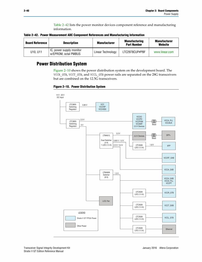
2–40 Chapter 2: Board ComponentsPower Supply
Table 2–42 lists the power monitor devices component reference and manufacturing information.
Power Distribution SystemFigure 2–10 shows the power distribution system on the development board. The VCCR_GTB, VCCT_GTB, and VCCL_GTB power rails are separated on the 28G transceivers but are combined on the 12.5G transceivers.
Table 2–42. Power Measurement ADC Component References and Manufacturing Information
Board Reference Description Manufacturer ManufacturingPart Number
Manufacturer Website
U10, U11 IC, power supply monitor w/EPROM, octal PMBUS Linear Technology LTC2978CUP#PBF www.linear.com
Figure 2–10. Power Distribution System
LEGEND
Stratix V GT FPGA Power
Other Power
Bead
Bead
1.5 V
0.85 V / 1.0 V
14 V - 20 VDC Input
LTC3855SwitchingRegulator
0.85 V VCCVCCHIP
VCCHSSI
5 V
LTC3855SwitchingRegulator
2.5 V
3.3 V3.3 V DevicesLTM4615
Dual Switcher(4 A)
1 LDO (1.5 A)
LTM4608Switcher
(8 A)
VCCIOVCCPD
VCCPGMVCCBAT
2.5 V Devices
2.5 V / 3.0 V
VCCA_GXB
LCD, Fan
VCCA_PLLVCCAUX
SFP+
VCCH_GXBVCCD_PLL
VCCPT
1.8 VLTC3026LDO (1.5 A)
LTC3026LDO (1.5 A)
LTC3026LDO (1.5 A)
LTC3026LDO (1.5 A)
LTC3026LDO (1.5 A)
XFP
VCCRT_GXB
VCCR_GTB
VCCT_GXB
VCCL_GTB
Ethernet
Transceiver Signal Integrity Development Kit January 2016 Altera CorporationStratix V GT Edition Reference Manual
Chapter 2: Board Components 2–41Power Supply
Temperature SenseThe Stratix V GT die uses a MAX1619 temperature sense device for temperature monitoring. The device connects to the MAX II CPLD EPM2210 System Controller and the Stratix V GT device by a 2-wire SMB interface. The MAX1619 device is located at slave address 0011000b (18h).
The OVERTEMPn and TSENSE_ALERTn signals are driven by the MAX1619 temperature sense device based on a programmable threshold temperature. The OVERTEMPn signal is driven to the MAX II System Controller. An over-temperature warning LED (D7) indicates the temperature fault condition.
Table 2–43 lists the temperature sense interface pin assignments, signal names, and functions.
Table 2–44 lists the temperature sense component reference and manufacturing information.
Table 2–43. Temperature Sense Pin Assignments, Schematic Signal Names, and Functions
Board Reference
(U12)
Schematic Signal Name
I/O Standard
MAX II CPLD System Controller
Pin Number
Stratix V GT Device
Pin NumberDescription
14 SMBCLK_TEMP 3.3-V D3 B8 SMB clock
12 SMBDATA_TEMP 3.3-V C2 A8 SMB data
11 ALERTn 3.3-V D2 E8 Programmable alert
9 OVERTEMPn 3.3-V E4 E7 Fan enable
3 TEMPDIODE_P 3.3-V — V11 Current source and remote diode input
4 TEMPDIODE_N 3.3-V — U11 Remote diode input
Table 2–44. Temperature Sense Component Reference and Manufacturing Information
Board Reference Description Manufacturer ManufacturingPart Number
Manufacturer Website
U12 Temperature sense, remote and local, programmable alert. Maxim MAX1619MEE+T www.maxim-ic.com
January 2016 Altera Corporation Transceiver Signal Integrity Development KitStratix V GT Edition Reference Manual

2–42 Chapter 2: Board ComponentsStatement of China-RoHS Compliance
Statement of China-RoHS ComplianceTable 2–45 lists hazardous substances included with the kit.
Table 2–45. Table of Hazardous Substances’ Name and Concentration Notes (1), (2)
Part Name Lead (Pb)
Cadmium (Cd)
Hexavalent Chromium
(Cr6+)
Mercury (Hg)
Polybrominatedbiphenyls (PBB)
Polybrominateddiphenyl Ethers
(PBDE)
Stratix V GT transceiver signal integrity development board X* 0 0 0 0 0
14 V power supply 0 0 0 0 0 0
Type A-B USB cable 0 0 0 0 0 0
User guide 0 0 0 0 0 0
Notes to Table 2–45:
(1) 0 indicates that the concentration of the hazardous substance in all homogeneous materials in the parts is below the relevant threshold of the SJ/T11363-2006 standard.
(2) X* indicates that the concentration of the hazardous substance of at least one of all homogeneous materials in the parts is above the relevant threshold of the SJ/T11363-2006 standard, but it is exempted by EU RoHS.
Transceiver Signal Integrity Development Kit January 2016 Altera CorporationStratix V GT Edition Reference Manual
January 2016 Altera Corporation
Additional Information
This chapter provides additional information about the document and Altera.
Board Revision HistoryThe following table lists the versions of all releases of the Stratix V GT transceiver signal integrity development board.
Document Revision HistoryThe following table shows the revision history for this document.
How to Contact AlteraTo locate the most up-to-date information about Altera products, refer to the following table.
Date Version Changes
December 2015 Production silicon New device part number—5SGTMC7K3F40C2.
January 2013 Production silicon New device part number—5SGTMC7K2F40C2.
February 2012 Engineering silicon Initial release.
Date Version Changes
January 2016 1.3 Revised the FPGA device part number
May 2014 1.2 Corrected ALM amount in the “Board Component Blocks” section and in Table 2–2.
January 2013 1.1
■ Revised the FPGA device part number for production silicon release.
■ Added Table 2–41 on page 2–39 to define the voltage levels for VCCRT_GXB and VCCA_GXB voltage rails.
■ Removed appendix A and appended the board revision history table in “Additional Information” chapter.
February 2012 1.0 Initial release.
Contact (1) Contact Method Address
Technical support Website www.altera.com/support
Technical trainingWebsite www.altera.com/training
Email [email protected]
Product literature Website www.altera.com/literature
Nontechnical support (general) Email [email protected]
(software licensing) Email [email protected]
Note to Table:
(1) You can also contact your local Altera sales office or sales representative.
Transceiver Signal Integrity Development KitStratix V GT Edition Reference Manual

1–2 Additional InformationAdditional InformationTypographic Conventions
Typographic ConventionsThe following table shows the typographic conventions this document uses.
Visual Cue Meaning
Bold Type with Initial Capital Letters
Indicate command names, dialog box titles, dialog box options, and other GUI labels. For example, Save As dialog box. For GUI elements, capitalization matches the GUI.
bold typeIndicates directory names, project names, disk drive names, file names, file name extensions, software utility names, and GUI labels. For example, \qdesigns directory, D: drive, and chiptrip.gdf file.
Italic Type with Initial Capital Letters Indicate document titles. For example, Stratix IV Design Guidelines.
italic typeIndicates variables. For example, n + 1.
Variable names are enclosed in angle brackets (< >). For example, <file name> and <project name>.pof file.
Initial Capital Letters Indicate keyboard keys and menu names. For example, the Delete key and the Options menu.
“Subheading Title” Quotation marks indicate references to sections in a document and titles of Quartus II Help topics. For example, “Typographic Conventions.”
Courier type
Indicates signal, port, register, bit, block, and primitive names. For example, data1, tdi, and input. The suffix n denotes an active-low signal. For example, resetn.
Indicates command line commands and anything that must be typed exactly as it appears. For example, c:\qdesigns\tutorial\chiptrip.gdf.
Also indicates sections of an actual file, such as a Report File, references to parts of files (for example, the AHDL keyword SUBDESIGN), and logic function names (for example, TRI).
r An angled arrow instructs you to press the Enter key.
1., 2., 3., anda., b., c., and so on
Numbered steps indicate a list of items when the sequence of the items is important, such as the steps listed in a procedure.
■ ■ ■ Bullets indicate a list of items when the sequence of the items is not important.
1 The hand points to information that requires special attention.
h The question mark directs you to a software help system with related information.
f The feet direct you to another document or website with related information.
m The multimedia icon directs you to a related multimedia presentation.
c A caution calls attention to a condition or possible situation that can damage or destroy the product or your work.
w A warning calls attention to a condition or possible situation that can cause you injury.
The envelope links to the Email Subscription Management Center page of the Altera website, where you can sign up to receive update notifications for Altera documents.
The feedback icon allows you to submit feedback to Altera about the document. Methods for collecting feedback vary as appropriate for each document.
Transceiver Signal Integrity Development Kit January 2016 Altera CorporationStratix V GT Edition Reference Manual


