1 Transmission Electron Microscopy Nicola Pinna Department of Chemistry, CICECO, University of Aveiro, 3810-193 Aveiro, Portugal. School of Chemical and Biological Engineering, College of Engineering, Seoul National University (SNU), Seoul 151-744, Korea E-mail: [email protected] - [email protected]Literature
Transcript
1
Transmission Electron Microscopy
Nicola Pinna
Department of Chemistry, CICECO, University of Aveiro, 3810-193 Aveiro, Portugal.
School of Chemical and Biological Engineering, College of Engineering, Seoul National University (SNU), Seoul 151-744, Korea
Brief HistoryThe electron microscope was first proposed by Knoll and Ruska in 1932
M. Knoll, E. Ruska, Das Elektronenmikroskop, Z. Phys. 78, 318-339 (1932)
In this paper they developed the idea of electron lenses into a practical reality and demonstrated electron images taken on the instrument shown in the next page
3
High resolution electron microscope constructed by Ruska at the Institute for Electron Microscopy at Fritz Haber Institute of the Max Planck Society (Berlin).
Operator: Klaus Weiss
4
Philips CM200 FEG at the Fritz Haber Institute (~ 1998)
Jeol 2200FS at the Humboldt University Berlin (~ 2007)
5
Limitations of the TEM
1) TEM is not a good sampling tool
Before putting your sample in the TEM you must have examined it by other techniques that offer poorer resolution but better sampling (e.g. your eyes, an optical microscope or a SEM)2) Electron beam damageA detrimental effect of ionizing radiation is that it can damage your specimen, particularly polymers (and most organics) and even certain minerals and ceramics
3) Specimen preparationA specimen has to be “thin” if you want to obtain information using transmitted electrons.“Thin” = electron transparentIn general < 100 nm, but this depends on the material and on the incident electron energyMethods to prepare thin specimens exist for almost all the materials but it is still a challenging, difficult and time consuming process. Moreover, it may introduce artifacts due to the chemical and structural modification of the specimen
4) Interpretation of the TEM images
Our eyes and brain routinely understand reflected light images but are ill-equipped to interpret TEM images and so we must be cautious
This problem is well illustrated by the picture of the two rhinoceros side by side such that the head of one appears attached to the rear of the other
One problem is that the TEM presents us with 2D images of 3D specimens, viewed in transmission
6
Electron sourcesTwo kinds of electron sources are used in the TEMs (and also SEMs)The first one is called a thermionic source. It “produces” electrons when heated. The second type is a field emission source. It “produces” electrons when a large electric potential is applied between it and the anode
Schottky sources combine both heat and field emission Here, we do not need to know much about how the electron sources work
We should at least keep in mind that field emission sources give more monochromatic electrons (i.e. energy spread of the electrons is lower)
Electron GunThe gun (thermionic) is composed of an electron source (e.g. the LaB6 crystal) the cathode, an anode kept at earth potential and a grid (Wehnelt cylinder)
When the electrons leave the cathode they have a negative potential with respect to the earthed anode
They accelerate through this potential acquiring the desired energy (100-400 KeV)
A small negative bias is applied to the Wehnelt cylinder in order to control the beamThe electrons coming off the cathode see the negative field and are converged to a point called a crossover between the Wehnelt and the anode
7
Electron lenses, aperturesThe electrons are “manipulated” by electromagnetic lenses
The focus, intensity of illumination and magnification can be changed by modifying the current through the lenses
An aperture is used to select different electron beams to form different images, thus manipulating the image contrast
Another aperture is used to select different regions of the specimen to contribute to the diffraction pattern
So, knowing how these apertures/lens combination work allows the operator to understand how to control the TEM and why some operations on the microscope are done
The illumination systemThe illumination system takes the electrons from the gun and transfer them to the specimen giving either a broad beam or a focused beam entering the specimen
Parallel beamIn traditional TEM mode, the first two condenser lenses (C1,C2) are adjusted to illuminate the speciment with a parallel beam of electrons
This operation mode is used for classical imaging and diffraction
8
Convergent Beam (STEM mode)In some case we want to minimize the size of the probe hitting the specimen as in scanning TEM (STEM) or for analytical TEM
The imaging systemThe objective lens takes the electrons from the exit surface of the specimen and disperses them to create a diffraction pattern in the back-focal plane and recombines them to form an image in the image plane
Diffraction mode: The back focal plane of the objective lens acts as the object plane for the intermediate lens
Image mode: The intermediate lens is adjusted in a way that its object plane is the image plane of the objective lens
9
The operation modesLow Magnification
In low magnification mode, the contrast observed on the viewing screen is caused by electrons that have been lost from the imaged region either by large-angle scattering outside the objective aperture (contrast aperture) or as a result of energy loss and wavelength change in the specimen (mass-thickness contrast).
Electrons that have lost some of their kinetic energy get focused on a plane far distant from the viewing screen. This out-of-focus “inelastic” or energy loss image only contributes a uniform background to the in-focus elastic image.
In the so-called bright-field mode, the objective aperture selects the direct, unscattered spot and excludes all electrons that were Bragg-scattered to higher angles, whereas in the dark-field mode the image is formed only from scattered electrons.
The possibility to select electrons according to a certain range of scattering angle allows to point out sample areas with different scattering characteristics like crystal defects in mono-crystals or micro-crystals of different orientation in polycrystalline samples.
Bright and dark field modesIn bright filed mode the objective aperture can be used to select only the direct beam. This permits to enhance the contrast because the scattered electrons will not contribute to the image
10
Bright and dark field modesThe objective aperture can be used to select a particular diffracted beam only
In this case the obtained image will be formed by electrons that are scattered in only a specific direction -> Dark field mode
Electron Diffraction
In this mode, the electron microscope is used as a diffractometer. This is simply done by changing the excitation of the intermediate lens system such that instead of focusing on the first image plane of the objective lens, it is focused on the back focal plane of the objective which contains the Fraunhoferdiffraction pattern.
The projector lens then projects a magnified image of the diffraction pattern on the fluorescent screen. The easy switch over from imaging to diffraction and vice versa and the variability of the electron probe size is very helpful for analytical work.
Small single crystals down to the size of 5 nm can be selected in image mode and their diffraction characteristic can be studied simply by changing to the diffraction mode. The arrangement and intensity of diffraction spots is related to the symmetry and dimension of the unit cell and depends on the orientation of the particle with respect to the incident beam.
11
Phase-Contrast ImagesHigh resolution transmission electron microscopy (HRTEM) is one of the most powerful tools used for the characterization of nanomaterials. The most important contrast mechanism for high resolution electron microscopy is phase-contrastIf the specimen is suitably thin for HRTEM, i.e. less than about 50 nm, the interaction of the electron beam with the inner potential of the specimen predominantly causes phase shifts of parts of the electron wave frontA phase contrast image requires the selection of more than one beam (direct + diffracted)Two beams can interfere to give an image with a periodicity related to |∆g|-1. Since one beam is the direct beam, |∆g|-1 is just d the interplanar spacing corresponding to gIf the beam is aligned parallel to a low-index zone axis, fringes running in different direction are observed. These fringes correspond to an array of spots in the diffraction pattern
The image interpretation in HRTEM is not straight forward. This is because in addition to the interaction of the electron beam with the specimen, also the effect of the imaging process by imperfect electron lenses has to be considered. The way how the microscope transfers waves with different relative phase shifts down through the column is defined by the so called contrast transfer function. It depends on the performance of the objective lens (spherical aberration), the acceleration voltage and the focus conditions. Further, chromatic aberrations, focal and energy spread of the beam and instabilities in the high tension and objective lens current play a role in the contrast formation.Assistance in the interpretation of HRTEM images is provided by image processing and image simulation.
12
Scanning Transmission Electron Microscopy
In the scanning mode (STEM), the specimen is scanned across the region of interest by using a very small probe of typically only a few Å in diameter.
If the specimen region is sufficiently thin, most electrons are transmitted withrelatively little lateral spreading, and a variety of signals from elastic and inelastic scattering events can be recorded, allowing high spatial resolution analysis and imaging.
At each point, various types of signals discriminated by scattering angle and energy loss yield different structural and chemical information that can be captured simultaneously in different channels. Most commonly, energy dispersive X-ray spectroscopy (EDX), electron energy loss spectrometry (EELS) and high angle annular dark field detectors (HAADF) are applied.
Diffraction in TEM
✔ wavelength of fast moving electrons much smaller than spacing of atomic planes => diffraction from atomic planes (e.g. 200 kV e-, λ = 0.0025 nm)✔ electrons interact very strongly with matter => strong diffraction intensity(can take patterns in seconds, unlike X-ray diffraction)✔ spatially-localized information (≳ 200 nm for selected-area diffraction; 2 nm possible with convergent-beam electron diffraction)✔ close relationship to diffraction contrast in imaging ✔ orientation information✔ immediate in the TEM!
(✘ diffraction from only selected set of planes in one pattern - e.g. only 2D information)(✘ limited accuracy of measurement - e.g. 2-3%)(✘ intensity of reflections difficult to interpret because of dynamical effects)
Why use electron diffraction?
Diffraction: constructive and destructive interference of waves
13
Elastic scattering theoryIsolated Atoms Collective scattering from
many atoms together
Particle description of the electrons Wave description of the electrons
14
The Rutherford differential cross section cannot be used to calculate the cross section exactly, because it ignores the wave nature of the electron beam
The most familiar aspect of the wave approach to cross sections is the concept of the atomic-scattering factor f(θ), which is related to the differential cross section by:
f(θ) is a measure of the amplitude of an electron wave scattered from an isolated atom
|f(θ)|2 is proportional to the scattered intensity
The scattering factor approach is complementary to the Rutherford differential cross section analysis, because it is most useful for describing the low angle elastic scattering
fx is the scattering factor for X-rays
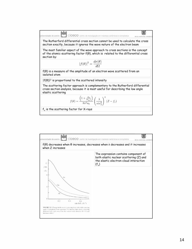
f(θ) decreases when θ increases, decreases when λ decreases and it increases when Z increases
The expression contains component of both elastic nuclear scattering (Z) and the elastic electron-cloud interaction (fx)
15
We can describe the incident beam as a wave of amplitude ψ0 and phase 2πkr
When it is scattered by ascattering centre, a sphericalscattered wave is created, whichhas amplitude ψsc but the samephase:
where f(θ) is the atomic scatteringfactor, k the wave vector of theincident or scattered wave, and rthe distance that the wave haspropagated.
The origin of f(θ)
The structure factor F(θ)The next step is to generalize the idea of individual atoms scattering electrons and see what happens when the atoms are stacked together in a crystal structure-> F(θ): measure of the amplitude scattered by an unit cell of a crystal structures
F(θ) can be defined as the sum of the f(θ) terms for all the atoms (i) in the unit cell multiplied by a phase factor, which takes into account of the difference in phase between waves scattered from atoms on different but parallel atomic planes with the same Miller indices (hkl)
As a result the amplitude (and its square, the intensity) is influenced by the type of atom and the position of the atom in the cell (x,y,z) and the specific atomic planes (hkl)
-> the intensity of the diffracted beams is a maximum at specific angles because the interplanar spacings are very well defined
16
The variation of F(θ) with θ is equivalent to the radial intensity variation across the diffraction pattern
F(θ)
F(θ)
Simple diffraction conceptsTo interpret low-angle elastic scattering (which is primarily from the electron cloud) it is best to think in terms of electron waves and not in terms of particle-particle interactions (which characterize high angle Rutherford scattering)
Each center acts as a new source of a wave of the same wavelengthWhen more waves are present the waves can interfere with one another
Waves reinforce one another when they are in phase and cancel one another when they are out of phaseThe waves are in phase only in certain directions
There is invariably a zero-order wave that proceeds in the same direction as the incident wave, which in the TEM we will refer to as the direct beam of electrons
There are also higher order waves that propagate in forward directions that are at some fixed angle to the incident wave and they are called diffracted beams
17
Diffraction equations (Laue)The diffracted waves are in phase if the path difference between wave scattered by adjacent scattering centers is a whole number of wavelength hλ (h is an integer)
If the scattering centers (B and C) are spaced some distance apart (a) and the incident beam makes an angle θ1 with the line connecting the scattering centers and is diffracted at an angle θ2, then the path difference AB-CD is:
Generalization in three dimensions
If the 3 Laue equations are satisfied simultaneously a diffracted beam is produced (hkl are the indices of the diffracted beam)
Braggs’ description of diffractionThe waves behave as if they were reflected off atomic planesThe path difference between electron waves reflected from the upper and lower planes is (AB+BC)
If the “reflecting” hkl planes are spaced a distance d apart and the wave incident and reflected at and angle θB both AB and BC are equal to d sinθB and the total path difference is 2d sin θB
Bragg angles in the TEM are small due to the fact that λ is small (few pm)
Ex: calculate θB for the 111 planes in Cu (d=0.21 nm) for 100 Kev (λ=0.00370 nm)
-> θB = 0.00881 rads = 0.505°
We can approximate sin θ ~ θ in the TEM
18
Scattering from lattice planesIt does not matter how the atoms (the scattering centers) are distributed on the two planes.The scattering from any two points on planes P1 and P2 will produce the same difference 2d sinθ
Dynamical effectsDynamical scattering effects as very important in electron scattering because the electron beam interacts strongly with the atoms in the crystal
The beam that has been Bragg diffracted once can be diffracted back into the direct beam as it is in perfect Bragg orientation
The probability of this process increases with the thickness of the specimen
These effects make it difficult to extract valuable information from the diffracted intensities and complicate the study of the diffraction pattern in general
19
Electron diffraction patternsAmorphous carbon
polycrystalline
Single crystal
Convergent beam electron diffraction
The greater the angle of scatter, the further off center the electron hits the film (or detector)
Most of the intensity is in the direct beam, in the center of the pattern
The scattered intensity decreases with increasing θ, which reflect the decrease in the scattering cross section
The scattering intensity varies strongly with the structure of the specimen
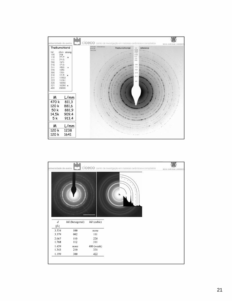
Diffraction in the TEMThe questions that can be addressed using electron diffraction patterns obtained in the TEM are the following:- Is the specimen crystalline?
- What are the crystallographic characteristics of the specimen (lattice parameters, symmetry, etc.)?- Is the specimen monocrystalline? - What is the orientation of the specimen with respect to the electron beam?- Is more than one phase present in the specimen?
20
Indexing diffraction patternsAs you know a particular crystal plane is defined by the Miller indices (hkl)We define the direct beam as the 000 reflection, and each diffracted beam, due to the diffraction from a specific (hkl) plane, with the corresponding hklindices
If we assign hkl to g, then the second order spot (2g) is 2h 2k 2l, etc.
If we look along a zone axis in a crystal (zone axis is the direction along the intersection of two or more planes) we will see sets of planes in the edge-on orientation
If there are many planes close to the Bragg orientation, then we will see many spots from many different planes
The magnification of the diffraction pattern can be described by the camera length (L)
If we increase the magnification of the lenses between the specimen and the viewing screen, we increase the effective distance L between the specimen and the screenThe camera length is a calculated value rather than a physical distance
If the electrons are scattered through an angle 2θ at the specimen, then the distance between the direct and the diffracted beams as measured on the screen (R) is determined by L:
From the Bragg equation we know that:
We can use this relation to determine crystal spacing (d)
L is determined by calibration from known specimens


![Ultrafast transmission electron microscopy using a laser ...transmission electron microscopy [4], scanning electron microscopy [5], x-ray diffraction [6], scanning tunneling and atomic](https://static.documents.pub/doc/80x56/607eb1335ce8082131294459/ultrafast-transmission-electron-microscopy-using-a-laser-transmission-electron.jpg)


