34
Description of transmitter firmwares for the Pulsar board Author: Tomi Mansikkala Wednesday, July 21, 2004
Description of transmitter firmwares for the Pulsar boardAuthor: Tomi MansikkalaWednesday, July 21, 2004
Contents
1. Introduction.........................................................................................................2
2. Common features for all the DataIO TX firmware.............................................3
3. Common features for all the Control TX firmware............................................6
3.1 XTRP/SVT transmitter................................................................................7
3.2 SLINK transmitter.......................................................................................8
4. Firmware versions.............................................................................................11
4.1 DataIO FPGA transmitters.........................................................................11
4.2 Control FPGA transmitters........................................................................13
5. Test pattern requirements..................................................................................14
6. Test pattern examples.......................................................................................15
7. VME address maps...........................................................................................20
7.1 Common Control FPGA VME address map.............................................20
7.1.1 VME software address map for internal TX RAM.............................20
7.2 Common DataIO FPGA VME address map..............................................21
7.2.1 VME software address map for internal TX RAM.............................21
7.2.2 Address map for Quartus II simulation...............................................22
8. Appendices........................................................................................................23
1

1. Introduction
This documentation describes transmitter firmware features for the Pulsar board.
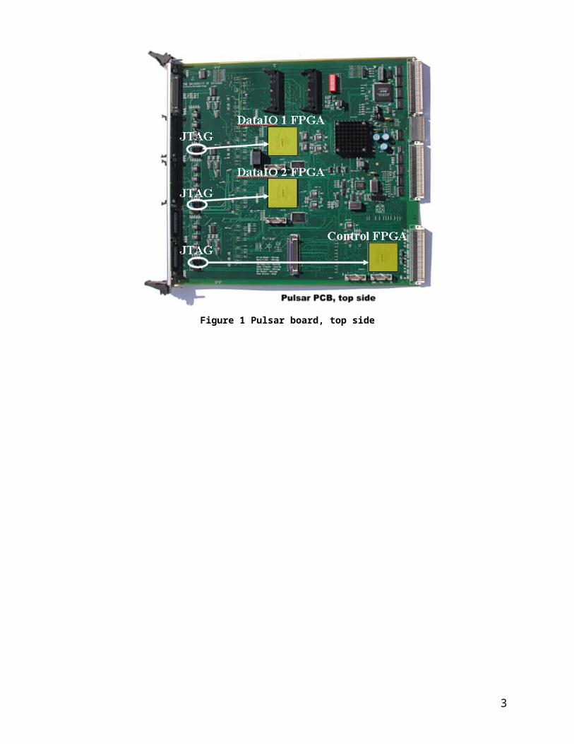
Pulsar board has three programmable FPGA chips, two for dataIO and one for control.These FPGAs are programmable thru JTAG connectors, which are located as figure 1 shows.Both dataIO FPGAs have connections to control FPGA, XTRP/SVT in/out connector, mezzanine cards (hotlink, taxi, S-LINK…) and also to VME chip.Control FPGA has connections between both dataIO FPGAs, XTRP/SVT in/out connector, AUX card and also to VME chip.Both dataIO FPGAs are capable to drive two mezzanine cards at simultaneously.
Transmitter’s basic idea is to simulate real system as well as possible and this is done by designing transmitter firmware which is capable to have all of the real system’s features like delays, gaps, etc.Transmitter firmware has internal memory where user can load test patterns. These test patterns reminds like real data which comes from Level 1 to Level 2 triggering system.Transmitter sends test pattern thru different interfaces like XTRP/SVT and Hotlink over to Pulsar receiver. This is the way how we test our Pulsar boards. More detailed information about VME software and Pulsar testing can be found from Frans Marjamaa’s document ‘Testing of Pulsar firmwares’.
Figure 1 Pulsar board, top side
2
2. Common features for all the DataIO TX firmware
DataIO transmitter firmware’s
- CLIST- ISOLIST- RECES- MUON
Figure 2 DataIO FPGA firmwares
3
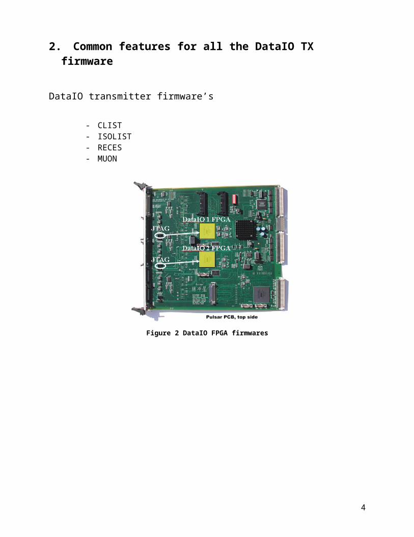
Figure 2 shows dataIO FPGA firmware locations on the board.
Figure 3 is a detailed picture about one of the transmitter main components, Out1ch. Each channel has 1k word internal RAM, where user can load test patterns thru VME. Data goes to output FIFO, which is 256 words deep, after receiving L1A and buffer number from P2 backplane. Delay counter starts from CDFL1A and ends when delay value has run out.When delay value has run out data is sent out from the FIFO.Delay and gap word values are 8 bits and counts on mezzanine clock.
Figure 3 Out1ch component
Transmitters can- send different events on each L1A- have delay before sending data (transmitter doesn’t send out delay words)- have gaps between data words (transmitter doesn’t send out gap words)- have empty events (transmitter doesn’t send out anything on certain L1As)

User has to write/read to/from the internal RAM by using write/read low and write/read high addresses. First 32bit word is used for data to all four channels (low word) and the next 20bit word is used for control bits to all four channels (high word).
Minimum delay valuesISOLIST minimum delay value (uses mezzanine card clock, with 64MHz roboclock) from simulation: ~ 32 mezzanine clocks and from tests: ~12 mezzanine clocks.CLIST minimum delay value (using mezzanine cards clock, with 64MHz roboclock) from simulation: ~ n/a mezzanine clocks and from tests: ~ 18 mezzanine clocks.MUON minimum delay value (using mezzanine (4*CDFCLK) clock ~30MHz) and from simulation: ~ n/a mezzanine clocks and from tests: ~ n/a mezzanine clocks.Minimum gap delay value from simulation and tests are 4 clocks.Gap delay times can be measured by using this formula: Gap value + 4
Bit descriptionsData bits are: 0-31 (= low word) Control bits are: 0-19 (= high word)
Bits 15, 10, 5, 0: Delay (all channels) Data, 8bit determines delay valueBits 16, 11, 6, 1: Gap (all channels) Data, 8bit determines gap delay valueBits 17, 12, 7, 2: Empty event (all channels) Data is not usedBits 18, 13, 8, 3: EoE (all channels) Data usedBits 19, 14, 9, 4: Terminator (all channels) Data used
Table 1 Control bits to all four channels
Control bits: 19 18 17 16 15 14 13 12 11 10 9 8 7 6 5 4 3 2 1 0
Example: 4channels
Delay: 1 1 1 1 0x8421Gap: 1 1 1 1 0x10842Empty event: 1 1 1 1 0x21084EoE: 1 1 1 1 0x42108EoE with Terminator: 1 1 1 1 1 1 1 1 0xC6318 ch 3 ch 2 ch 1 ch 0
5

3. Common features for all the Control TX firmware
Control transmitter firmware’s- XTRP (also implemented input)- SVT (also implemented input)- SLINK (also implemented input)
Figure 4 Control FPGA firmwares
Figure 4 shows control FPGA firmware locations on the board.
Figure 5 is a detailed picture about one of the transmitter main components, Out1ch. Firmware has 4k word internal RAM, where user can load test patterns thru VME. Data goes to output FIFO, which is 1024 words deep, after receiving L1A and buffer number from P2 backplane. Delay counter starts from CDFL1A and ends when delay value has run out.When delay value has run out data is sent out from the FIFO. Transmitter firmware adds bunch counter value and buffer number to the end of event word.Delay and gap word values are 12 or 16bits and counts on CDFCLK on XTRP transmitter and SLINK clock on SVT and SLINK transmitters.Input data is stored to DAQ2 RAM which is 1024 words deep for XTRP/SVT and 256 for SLINK.
6
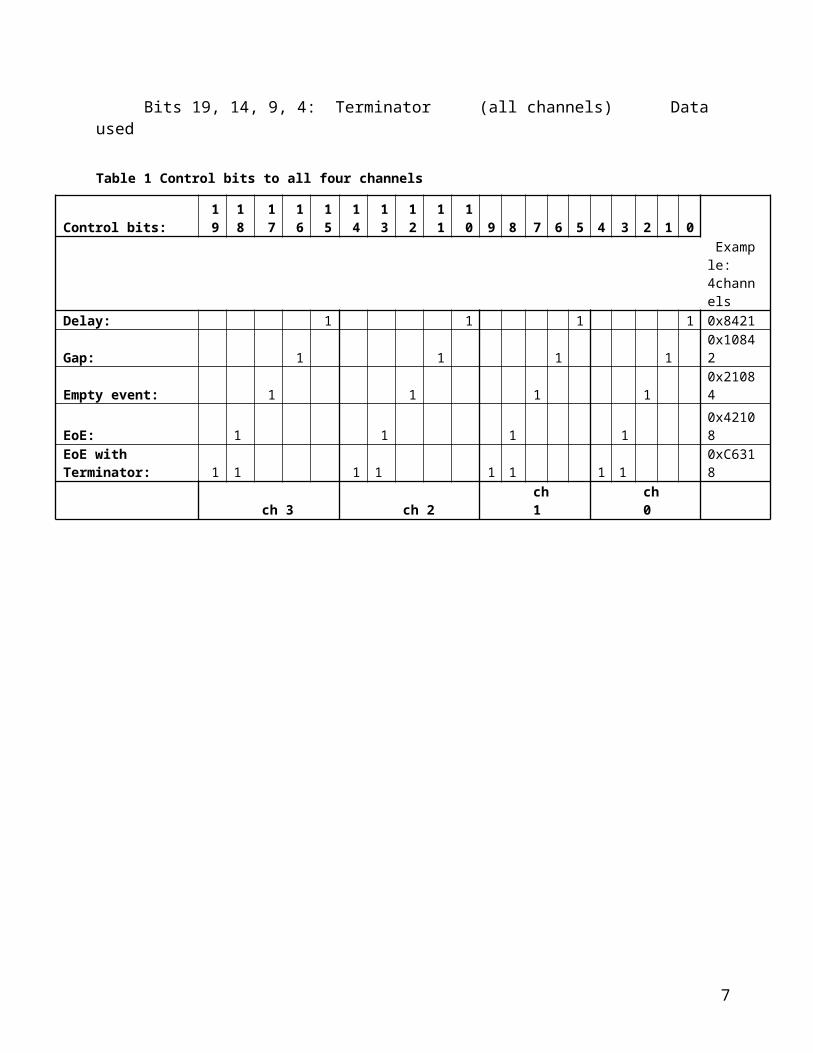
Figure 5 Out1ch component
Transmitters can- send different events on each L1A- have delay before sending data (transmitter doesn’t send out delay words)- have gaps between data words (transmitter doesn’t send out gap words)- have empty events (transmitter doesn’t send out anything on certain L1As)
3.1 XTRP/SVT transmitterUser can write/read to/from the internal RAM by using one write/read address.Transmitter is disabled by default (uses pass thru REAL data feature) and it’s needed to be enabled via VME.0 default = uses pass thru REAL data feature1 = uses transmitters own RAMPass thru real data mode means that incoming data from XTRP/SVT input connector is stored to one of the firmware’s DAQ RAMs which is 1024 words deep and the same time data is sent out thru XTRP/SVT output connector.Pass thru time is time between first word comes in and the first word goes out.
7

Minimum delay valuesPass thru time on simulation is 216ns for SVT transmitter and 1.584us for XTRP.SVT transmitter sends data out faster than XTRP because it uses SLINK clock.These measurements were made by using 60MHz SLINK clock, because then SVT transmitter sends data for 30MHz rate.XTRP minimum delay value from simulation is ~14 CDFCLK clock cycles and from tests ~11 CDFCLK clock cycles.SVT minimum delay value (measured by using 60MHz SLINK clock) from simulation is ~54 SLINK clocks and from tests ~50 SLINK clocks.Minimum gap delay value from simulation and test are 4 SLINK clocks.Gap delay times can be measured by using this formula: Gap value + 4
Bit descriptionsData bits are: 0-22Control bits are: 23-27
Bit 23: Delay Data, 12bits is used to determine delay valueBit 24: Gap Data, 12bits is used to determine gap delay valueBit 25: Empty event Data is not usedBit 26: EoE Data usedBit 27: Terminator Data used
3.2 SLINK transmitterUser has to write/read to/from the internal RAM by using write/read low and write/read high addresses. First 32bit word is used for data (low word) and the next 5bit word is used for control bits (high word).Firmware is also capable to receive and store SLINK data from AUX card and also measure time between sending first word out and receiving the last word. This time value can be read out thru VME.Incoming data from AUX card thru P3 connector is stored into one of the firmware’s DAQ RAMs, which are 256 words deep.
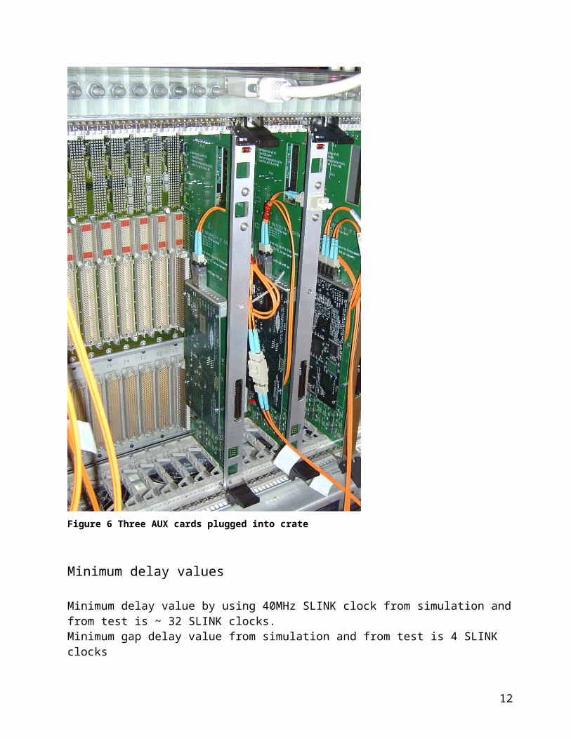
Figure 6 shows picture of three AUX cards plugged into test stand crate.LSC (link source card = transmitting SLINK card) is located on the left side of the AUX card and LDC (link destination card = receiving SLINK card) on the right side when AUX card is plugged into crate.
8
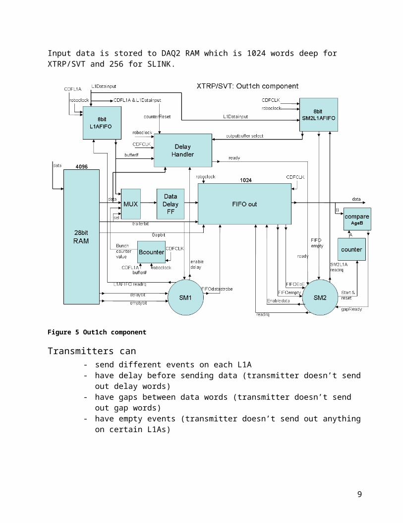
Figure 6 Three AUX cards plugged into crate
Minimum delay values
Minimum delay value by using 40MHz SLINK clock from simulation and from test is ~ 32 SLINK clocks.Minimum gap delay value from simulation and from test is 4 SLINK clocksGap delay times can be measured by using this formula: Gap value + 4
9

Bit descriptionsData bits are: 0-31 (= low word) Control bits are: 0-4 (= high word)
Bit 0: Delay Data, 16bits is used to determine delay valueBit 1: Gap Data, 16bits is used to determine gap delay valueBit 2: Empty event Data is not usedBit 3: EoE Data usedBit 4: Terminator Data used
Table 2 Control bits for SLINK TX
Control bits: 4 3 2 1 0 Delay: 1 0x01Gap: 1 0x02Empty event: 1 0x04EoE: 1 0x08EoE with Terminator: 1 1 0x18
10

4. Firmware versions
All the new transmitters (source codes, programming files) are located on NCDF159 PC and SVT test stand PC.
Path on NCDF159 PC is: C:\Users\Tomi\Pulsar configuration\TX\ <firmware type> Path on SVT test-stand PC is: C:\users\sakari\Pulsar firmware configuration\ <firmware type>
More detailed information about different firmware versions can be found from readme.txt file which are included to SVT test-stand PC. Path is C:\users\sakari\Pulsar firmware configuration\ <firmware type>.
4.1 DataIO FPGA transmitters
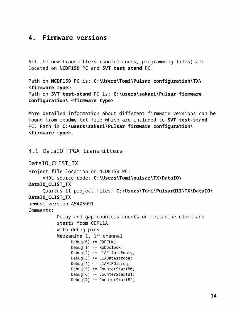
DataIO_CLIST_TXProject file location on NCDF159 PC:
VHDL source code: C:\Users\Tomi\pulsar\TX\DataIO\DataIO_CLIST_TXQuartus II project files: C:\Users\Tomi\PulsarQII\TX\DataIO\DataIO_CLIST_TX
newest version A5406091Comments:
- Delay and gap counters counts on mezzanine clock and starts from CDFL1A- with debug pins
Mezzanine 1, 1st channelDebug(0) <= CDFCLK;Debug(1) <= Roboclock;Debug(2) <= L1AFifordEmpty;Debug(3) <= L1ADatastrobe;Debug(4) <= L1AFIFOrdreq;Debug(5) <= CounterStartB0;Debug(6) <= CounterStartB1;Debug(7) <= CounterStartB2;Debug(8) <= CounterStartB3;Debug(9) <= SM2L1AFIFOrdreq;Debug(10) <= Ready;Debug(11) <= Datastrobe;Debug(12) <= Data8inputFIFOrdreq;Debug(13) <= Data8inputFifordEmpty;Debug(14) <= MezzEnaFIFOout;
11
DataIO_ISOLIST_TXProject file location on NCDF159 PC:
VHDL source code: C:\Users\Tomi\pulsar\TX\DataIO\DataIO_ISOLIST_TXQuartus II project files: C:\Users\Tomi\PulsarQII\TX\DataIO\DataIO_ISOLIST_TX
newest version A4406022Comments:
- can also be used as RECES transmitter- Delay and gap counters counts on mezzanine clock and starts from CDFL1A- with debug pins
Mezzanine 2, 3rd channel:Debug(0) <= CDFCLK;Debug(1) <= Roboclock;Debug(2) <= L1AFifordEmpty;Debug(3) <= L1ADatastrobe;Debug(4) <= L1AFIFOrdreq;Debug(5) <= CounterStartB0;Debug(6) <= CounterStartB1;Debug(7) <= CounterStartB2;Debug(8) <= CounterStartB3;Debug(9) <= SM2L1AFIFOrdreq;Debug(10) <= Ready;Debug(11) <= Datastrobe;Debug(12) <= Data8inputFIFOrdreq;Debug(13) <= Data8inputFifordEmpty;Debug(14) <= MezzEnaFIFOout;
DataIO_RECES_TXSame as ISOLIST TX
DataIO_MUON_TXProject file location on NCDF159 PC:
VHDL source code: C:\Users\Tomi\pulsar\TX\DataIO\DataIO_MUON_TXQuartus II project files: C:\Users\Tomi\PulsarQII\TX\DataIO\DataIO_MUON_TX
newest version A1406072Comments:
- without debug pins- Delay and gap counters counts on mezzanine clock and starts from CDFL1A
12

4.2 Control FPGA transmitters
Control_XTRP_TXProject file location on NCDF159 PC:
VHDL source codes: C:\Users\Tomi\Pulsar configuration\TX\Control_SVT_TX\XTRPQuartus II project files:C:\Users\Tomi\Pulsar configuration\TX\Control_SVT_TX\XTRP
newest version A6405193Comments:
- without debug pins- Implemented pass through mode- Added Bunch counter value and Buffer bit #s to header word- Delay and gap counters counts on CDFCLK clock and starts from CDFL1A- Input data is stored to DAQ2 RAM which is 512words deep
Control_SVT_TXProject file location on NCDF159 PC:
VHDL source codes: C:\Users\Tomi\pulsar\TX\Control\Control_SVT_TXQuartus II project files: C:\Users\Tomi\PulsarQII\TX\Control\Control_SVT_TX
newest version A7405250Comments:
- without debug pins- TX is now using SLINK clock to drive data out- Implemented pass through mode- Added Bunch counter value and Buffer bit #s to header word- Delay and gap counters counts on SLINK clock and starts from CDFL1A- Input data is stored to DAQ2 RAM which is 512words deep
Control_SLINK_TXProject file location on NCDF159 PC:
VHDL source codes: C:\Users\Tomi\pulsar\TX\Control\Control_Slink_TXQuartus II project files: C:\Users\Tomi\PulsarQII\TX\Control\Control_Slink_TX
newest version A0406300 Comments:
- without debug pins- Added SLINK input and time measure features- Slink input data is stored to DAQ2 RAM which is 256words deep- Test pattern RAM is 4k deep (not divided to buffers anymore) and 37 bits width (32
data bits + 5 control bits)- Delay and gap word values are 16 bits- Delay and gap counters counts on SLINK clock and starts from CDFL1A
13
5. Test pattern requirements
Process how to create test patterns are the same for every transmitter, only data word size differs.Every transmitter has five control bits: delay, gap, empty event, end of event (EoE) and terminator.Each events first word is a delay or empty event word and has to be marked with delay or empty event bit.Each events last word is end of event word and has to be marked with end of event bit.Adding terminator bit to end of event word user marks current event to the last event. After terminator bit RAM address counter is cleared and following event will be the first event from the RAM.
Special cases Sending only one word out (EoE):
- User needs to put two EoE word in successively Transmitter sends only the first EoE word
Creating empty events (disable channels):
- User needs to mark events first word by using empty event bit Transmitter doesn’t send anything out from that channel.
- User can disable different channels by using this feature.
14
6. Test pattern examples
Figure 7 shows an example how to create test patterns for the transmitters. Events first word is marked with a delay bit and data is used as delay value to delay transmission. Transmitter doesn’t send delay words.Event contains also two gap words which data is used to create gaps between transmitted words. Transmitter doesn’t send gap words.After end of event transmitter searches for the beginning of the next event (delay or empty event bit) by incrementing RAM address.More information how to design test patterns can be found from Frans Marjamaa’s document ‘Testing of Pulsar firmwares’.
Figure 7 Generic test pattern example
15

Figure 8 shows detailed example about XTRP/SVT test pattern.Events first word is marked with a delay bit. Delay value (12bit data) is 0x01F.Events sixth and tenth words are marked with a gap bit. Gap values (12bit data) are 0x00A and 0x02B.User has marked this event to the last event by using terminator bit. Next event will be the first event from the RAM.
Figure 8 Detailed SVT test pattern example
16

Figure 9 shows detailed example about SLINK test pattern.Example events first word is marked with a delay bit. Delay value (16bit data) is 0x0000.Events sixth and tenth words are marked with a gap bit. Gap values (16bit data) are 0x000A and 0x002B.User has marked this event to the last event by using terminator bit. Next event will be the first event from the RAM.
Figure 9 Detailed SLINK test pattern example
17
Figure 10 shows detailed test pattern example about all dataIO transmitters.Events first word is marked with a delay bit. Delay values (8bit data) are ch0: 0x22, ch1: 0x33, ch2: 0x44 and ch3: 0x55.Sixth word in channels 0 and 3 are marked with a gap bit. Gap values (8bit data) are ch0: 0x0A and ch3: 0x00.Tenth word in channels 0 and 1 are marked with a gap bit. Gap values (8bit data) are ch0: 0x2B and ch3: 0x08.User has marked this event to the last event by using terminator bit. Next event will be the first event from the RAM.
Figure 10 Detailed dataIO TX (CLIST, MUON, ISOLIST and RECES) test pattern example 1
18
Figure 11 shows detailed test pattern example about all DataIO transmitters.In this example channel 2 is disabled by using empty event bit. After empty event channel 2 searches for the next beginning of event and then waits until get L1A.Next event will be the seventh event from the RAM.
Figure 11 Detailed dataIO TX (CLIST, MUON, ISOLIST and RECES) test pattern example 2
7. VME address maps
7.1 Common Control FPGA VME address mapTable 3 Common VME addresses
Control FPGAFirmware version YY000000 (R)Reset YY000004 (W)DAQ SW version YY000008 (R/W)Control register 1 YY00000C (R/W)Status register 1 YY000010 (R)
Description Bits DataFirmware version 31…0 0xA6405180Reset FPGA - -DAQ SW version 31…0 Power-up value: 0Bunch Count Shift 7…0 Power-up value: 41Not used 31…0 0xC0FFEEEE
19

Pulse 1 YY000014 (W)Control register 2 YY000018 (R/W)Control register 3 YY00001C (R/W)Status register 2 YY000020 (R)Control register 4 YY000028 (R/W)
IDPROM YY100000 – YY10007C (R)
VMEL1A (=SLINK TX) - -Not used 31…0 Power-up value: 0Not used 31…0 Power-up value: 0Not used 31…0 0xDEADBEEFEnable TX (=XTRP&SVT)Enable VMEL1A (=SLINK TX)
0 Disable=0, Enable=1IDPROM 31…24
Read only register formatFirmware ID + Date + Version number 8-bits 20-bits 4-bits
Control input DAQWord countBuffer 0 YY000804Buffer 1 YY000904Buffer 2 YY000A04Buffer 3 YY000B04
ReadoutBuffer 0 YY820000Buffer 1 YY920000Buffer 2 YYA20000Buffer 3 YYB20000
IDPROM (example SVT TX)YY100000 Serial # YY100040 SYY100004 Serial # YY100044 VYY100008 Serial # YY100048 TYY10000C Serial # YY10004C YY100010 YY100050 TYY100014 0 YY100054 XYY100018 8 YY100058YY10001C 1 YY10005CYY100020 YY100060YY100024 P YY100064YY100028 U YY100068YY10002C L YY10006CYY100030 S YY100070YY100034 A YY100074YY100038 R YY100078YY10003C YY10007C
7.1.1 VME software address map for internal TX RAMTable 4 VME software address map
Control XTRP/SVT TX RAMWrite to RAM YY600000Reset RAM address YY600004Advance RAM YY600008Read from RAM YY60000C
Enable TX YY000028
Address map for Quartus II simulationWrite to RAM YY180000Reset RAM address YY180001Advance RAM YY180002Read from RAM YY180003
Enable TX YY000007
20

Table 5 VME software address map
Control SLINK TX RAMWrite low YY600000Write high YY600004Write activate YY600008Reset RAM address YY60000CRAM advance YY600010Read low YY600014Read high YY600018
Read time value YY60001C= time between first word OUT and last word IN# of SLINK clock cycles in hex
Address map for Quartus II simulationWrite low YY180000Write high YY180001Write activate YY180002Reset RAM address YY180003RAM advance YY180004Read low YY180005Read high YY180006
Read time value YY180007= time between first word OUT and last word IN# of SLINK clock cycles in hex
7.2 Common DataIO FPGA VME address mapTable 6 Common VME addresses
DataIO 1 FPGAFirmware version YY080000 (R)Reset YY080004 (W)Control register 1 YY080008 (R/W)Control register 2 YY08000C (R/W)Status register 1 YY080010 (R)Pulse 1 YY080014 (W)Control register 3 YY080018 (R/W)Control register 4 YY08001C (R/W)Status register 2 YY080020 (R)
DataIO 2 FPGAFirmware version YY0C0000 (R)Reset YY0C0004 (W)Control register 1 YY0C0008 (R/W)Control register 2 YY0C000C (R/W)Status register 1 YY0C0010 (R)Pulse 1 YY0C0014 (W)Control register 3 YY0C0018 (R/W)Control register 4 YY0C001C (R/W)Status register 2 YY0C0020 (R)
7.2.1 VME software address map for internal TX RAMTable 7 DataIO 1 FPGA
Mezzanine 1Write low YY580004Write high YY580008Write activate YY58000CReset address YY580010RAM advance YY580014Read low YY580018Read high YY58001C
Mezzanine 2Write low YY580020Write high YY580024Write activate YY580028Reset address YY58002CRAM advance YY580030Read low YY580034Read high YY580038
Table 8 DataIO 2 FPGA
Mezzanine 1Write low YY5C0004Write high YY5C0008Write activate YY5C000CReset address YY5C0010RAM advance YY5C0014Read low YY5C0018Read high YY5C001C
Mezzanine 2Write low YY5C0020Write high YY5C0024Write activate YY5C0028Reset address YY5C002CRAM advance YY5C0030Read low YY5C0034Read high YY5C0038
21

7.2.2 Address map for Quartus II simulationExample: FPGA_ID is low ‘0’ (DataIO1) and VME address bit 19 is high ‘1’ (DataIO1)Table 9 Addresses for Quartus II simulation
Mezzanine 1Write low YY160001Write high YY160002Write activate YY160003Reset address YY160004RAM advance YY160005Read low YY160006Read high YY160007
Mezzanine 2Write low YY160008Write high YY160009Write activate YY16000AReset address YY16000BRAM advance YY16000CRead low YY16000DRead high YY16000E
22

8. Appendices
Here are firmwares detailed pictures. More power point files and simulation screenshots can be found on NCDF159 PC at C:\Users\Tomi\Docs\Works\Firmware folder.
Figure 12 TXRAMTOFIFOinterface statemachine
23

Figure 13 Delay handler component
24
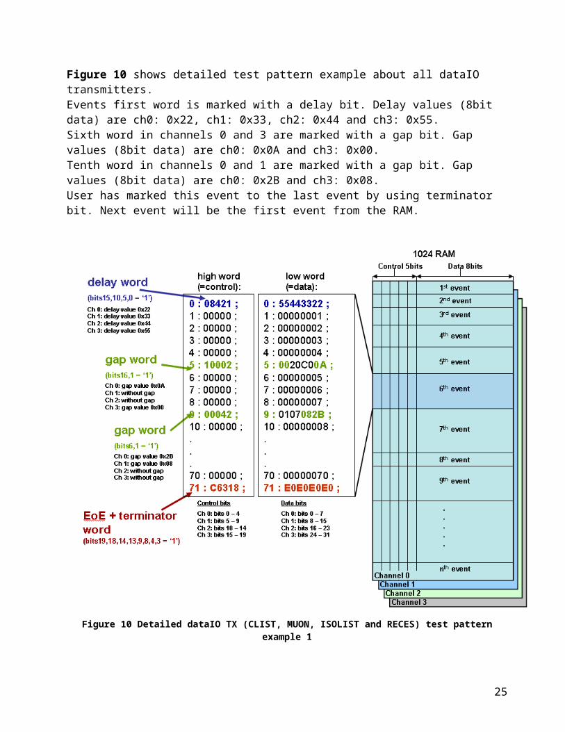
Figure 14 TXSTM state machine
25


![Design of Pulsar Board new.ppt [Read-Only]hep.uchicago.edu/~thliu/edg/Pulsar/Mini_review/Design_of_Pulsar_Board_new.pdfLevel 2 Pulsar – Status –July 24, 2002 • All the changes](https://static.documents.pub/doc/80x56/5fe358fd5cdba960c42cecd3/design-of-pulsar-board-newppt-read-onlyhep-thliuedgpulsarminireviewdesignofpulsarboardnewpdf.jpg)


![30 Strip Connector - University of Chicagohep.uchicago.edu/.../PSEC4_30ch_analog_rev1.pdf · 8 7 6 5 4 3 2 1 The University of Chicago ref_3 ref_2 ref_1 ref_6 ref_5 ref_4 CH6[1:0]](https://static.documents.pub/doc/80x56/5f7b8e9befa11352c333d0ae/30-strip-connector-university-of-8-7-6-5-4-3-2-1-the-university-of-chicago-ref3.jpg)


