Page 1
http://photonics.ee.auth.gr
G. Sinatkas1, D. C. Zografopoulos2, A. Pitilakis1, R. Beccherelli2, E. E. Kriezis1
1Dept. of Electrical & Computer Engineering, Aristotle University of Thessaloniki, Greece
2Istituto per la Microelettronica e Microsistemi, Consiglio Nazionalle delle Ricerche (CNR-IMM), Rome, Italy
18th European Conference on Integrated Optics 18 – 20 May, 2016 – Warsaw, Poland
SESSION #6 - ACTIVE DEVICES
Transparent Conducting Oxide Electro-Optic Modulators:
A Comprehensive Study based on the Drift-Diffusion Semiconductor Model
Page 2
ECIO 2016 – Warsaw • Georgios Sinatkas, Dept. of ECE, AUTH – Greece
Presentation Outline
2
Introduction
Transparent Conducting Oxides (TCOs)
TCO-based Electro-Optic Modulation
Motivation & Main Objectives
Multiphysics Modeling Framework
Solid-State Physics
Electromagnetic Modeling
SOI-based TCO Modulators
Silicon Rib Platform
Silicon Slot Platform
Summary & Conclusions
Page 3
ECIO 2016 – Warsaw • Georgios Sinatkas, Dept. of ECE, AUTH – Greece
Introduction
Transparent Conducting Oxide Electro-Optic Modulation
3
Page 4
ECIO 2016 – Warsaw • Georgios Sinatkas, Dept. of ECE, AUTH – Greece
Transparent Conducting Oxides
Introduction
4
Material n (cm-3) λp (μm)
Ag 5.86x10²² 0.14
ITO 6.17x10²⁰ 1.55
n-InSb 4.00x10¹⁸ 14.0
Page 5
ECIO 2016 – Warsaw • Georgios Sinatkas, Dept. of ECE, AUTH – Greece
Transparent Conducting Oxides
Introduction
5
Material n (cm-3) λp (μm)
Ag 5.86x10²² 0.14
ITO 6.17x10²⁰ 1.55
n-InSb 4.00x10¹⁸ 14.0
Page 6
ECIO 2016 – Warsaw • Georgios Sinatkas, Dept. of ECE, AUTH – Greece
ITO @ 1.55 μm
TCO-based Electro-Optic Modulation
Introduction
6
Page 7
ECIO 2016 – Warsaw • Georgios Sinatkas, Dept. of ECE, AUTH – Greece
Principle of TCO-based Electro-Optic Modulation
Switch between states of low and high mode loss by modulating the free-carrier concentration in the TCO
ENZ Effect: The guided modes polarized normally to the TCO layer suffer from increased losses (discontinuity of the electric field normal component)
ITO @ 1.55 μm
TCO-based Electro-Optic Modulation
Introduction
7
Page 8
ECIO 2016 – Warsaw • Georgios Sinatkas, Dept. of ECE, AUTH – Greece
Principle of TCO-based Electro-Optic Modulation
Switch between states of low and high mode loss by modulating the free-carrier concentration in the TCO
ENZ Effect: The guided modes polarized normally to the TCO layer suffer from increased losses (discontinuity of the electric field normal component) Low loss (ON state) Dielectric region, non = 1019 cm-3
ITO @ 1.55 μm
TCO-based Electro-Optic Modulation
Introduction
8
ON
Page 9
ECIO 2016 – Warsaw • Georgios Sinatkas, Dept. of ECE, AUTH – Greece
Principle of TCO-based Electro-Optic Modulation
Switch between states of low and high mode loss by modulating the free-carrier concentration in the TCO
ENZ Effect: The guided modes polarized normally to the TCO layer suffer from increased losses (discontinuity of the electric field normal component) Low loss (ON state) Dielectric region, non = 1019 cm-3 High Loss (OFF state) ENZ region, noff ~ 6x1020 cm-3
ITO @ 1.55 μm
TCO-based Electro-Optic Modulation
Introduction
9
ON
OFF
Page 10
ECIO 2016 – Warsaw • Georgios Sinatkas, Dept. of ECE, AUTH – Greece
Principle of TCO-based Electro-Optic Modulation
Switch between states of low and high mode loss by modulating the free-carrier concentration in the TCO
ENZ Effect: The guided modes polarized normally to the TCO layer suffer from increased losses (discontinuity of the electric field normal component) Low loss (ON state) Dielectric region, non = 1019 cm-3 High Loss (OFF state) ENZ region, noff ~ 6x1020 cm-3
ITO @ 1.55 μm
TCO-based Electro-Optic Modulation
Introduction
10
How can we control the TCO free-carrier concentration after fabrication? Using an external electric field attract/repel carriers forming accumulation/depletion regions
ON
OFF
Page 11
ECIO 2016 – Warsaw • Georgios Sinatkas, Dept. of ECE, AUTH – Greece
Motivation
Addressable and versatile TCO properties
Simplifications in describing semiconductor physics employing averaging or approximate techniques
Inaccuracy in bridging the gap between solid-state and wave physics
Understudied silicon-photonic platforms comprising TCOs
Main Objectives
Establish a comprehensive, multiphysics modeling framework for TCO-based devices
Design novel, high-performing, SOI-based TCO modulators comprising ITO
Motivation & Main Objectives
Introduction
11
Page 12
ECIO 2016 – Warsaw • Georgios Sinatkas, Dept. of ECE, AUTH – Greece
Multiphysics Modeling Framework
Solid-State & Wave Physics
12
Page 13
ECIO 2016 – Warsaw • Georgios Sinatkas, Dept. of ECE, AUTH – Greece
13
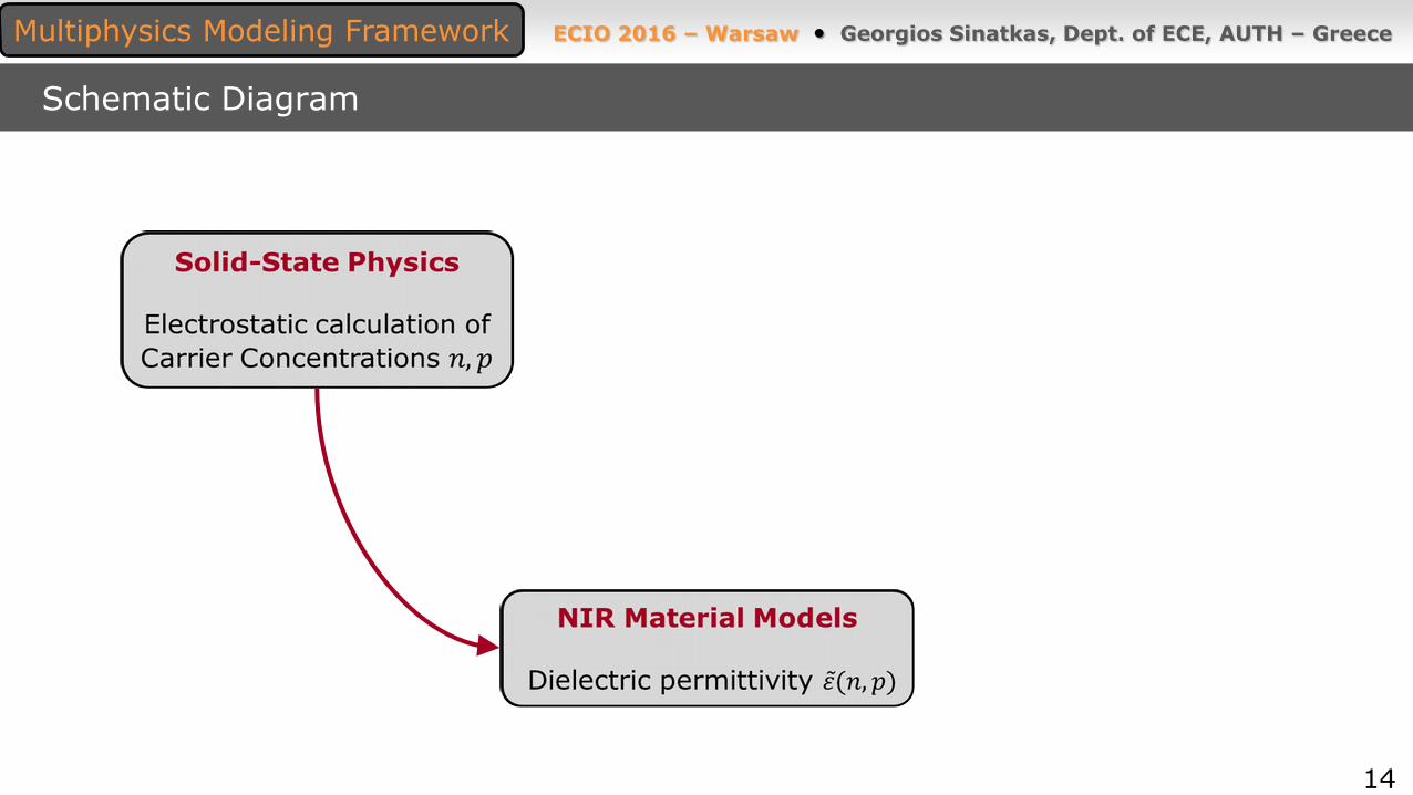
Schematic Diagram
Multiphysics Modeling Framework
Page 14
ECIO 2016 – Warsaw • Georgios Sinatkas, Dept. of ECE, AUTH – Greece
14
Schematic Diagram
Multiphysics Modeling Framework
Page 15
ECIO 2016 – Warsaw • Georgios Sinatkas, Dept. of ECE, AUTH – Greece
15
Schematic Diagram
Multiphysics Modeling Framework
Page 16
ECIO 2016 – Warsaw • Georgios Sinatkas, Dept. of ECE, AUTH – Greece
16
Schematic Diagram
Multiphysics Modeling Framework
Finite Element Method (FEM) Platform– COMSOL Multiphysics® Software
Page 17
ECIO 2016 – Warsaw • Georgios Sinatkas, Dept. of ECE, AUTH – Greece
Semiconductor Materials: Drift-Diffusion (DD) Model
Charge Conservation Law (Poisson Equation)
Current Conservation Laws
17
Solid-State Physics
Multiphysics Modeling Framework
Page 18
ECIO 2016 – Warsaw • Georgios Sinatkas, Dept. of ECE, AUTH – Greece
Semiconductor Materials: Drift-Diffusion (DD) Model
Charge Conservation Law (Poisson Equation)
Current Conservation Laws
DD Current Expressions
18
Solid-State Physics
Multiphysics Modeling Framework
Fermi-Dirac Carrier Distributions Essential for degenerately doped semiconductors such as TCOs
Page 19
ECIO 2016 – Warsaw • Georgios Sinatkas, Dept. of ECE, AUTH – Greece
Semiconductor Materials: Drift-Diffusion (DD) Model
Insulating Materials Laplace Equation
Charge Conservation Law (Poisson Equation)
Current Conservation Laws
DD Current Expressions
19
Solid-State Physics
Multiphysics Modeling Framework
Fermi-Dirac Carrier Distributions Essential for degenerately doped semiconductors such as TCOs
Page 20
ECIO 2016 – Warsaw • Georgios Sinatkas, Dept. of ECE, AUTH – Greece
Semiconductor Materials: Drift-Diffusion (DD) Model
Insulating Materials Laplace Equation
Boundary Conditions Semiconductor/Insulator Interfaces
Voltage Source Contacts
Charge Conservation Law (Poisson Equation)
Current Conservation Laws
DD Current Expressions
20
Solid-State Physics
Multiphysics Modeling Framework
Fermi-Dirac Carrier Distributions Essential for degenerately doped semiconductors such as TCOs
Ideal Ohmic
Page 21
ECIO 2016 – Warsaw • Georgios Sinatkas, Dept. of ECE, AUTH – Greece
21
The n-Si/HfO2/ITO Junction
Multiphysics Modeling Framework
Page 22
ECIO 2016 – Warsaw • Georgios Sinatkas, Dept. of ECE, AUTH – Greece
22
The n-Si/HfO2/ITO Junction
Multiphysics Modeling Framework
ND, Si = 1018 cm-3 increase
silicon conductivity
ND, ITO = 1019 cm-3 maintain
low wave losses (low loss ITO
dielectric behavior)
Positive bias Accumulation Layers
Negative bias Depletion Layers
Page 23
ECIO 2016 – Warsaw • Georgios Sinatkas, Dept. of ECE, AUTH – Greece
23
The n-Si/HfO2/ITO Junction
Multiphysics Modeling Framework
ND, Si = 1018 cm-3 increase
silicon conductivity
ND, ITO = 1019 cm-3 maintain
low wave losses (low loss ITO
dielectric behavior)
Positive bias Accumulation Layers
Negative bias Depletion Layers
Va > Vth = 3V ENZ region
EO Modulation: Toggle between 0 & >3V
nEZ = 6.17x10²⁰
Vth = 3V
Page 24
ECIO 2016 – Warsaw • Georgios Sinatkas, Dept. of ECE, AUTH – Greece
24
Schematic Diagram
Multiphysics Modeling Framework
Finite Element Method (FEM) Platform
Model for ITO Drude-like permittivity expression
[Kulkarni & Knickerbocker, J. Vac. Sci. Technol. A, 1996]
Model for Silicon [Soref & Bennett, IEEE J. Quantum Electron., 1987] [Nedeljkovic et al., IEEE Photon. J., 2011]
Page 25
ECIO 2016 – Warsaw • Georgios Sinatkas, Dept. of ECE, AUTH – Greece
25
Schematic Diagram
Multiphysics Modeling Framework
Finite Element Method (FEM) Platform
Page 26
ECIO 2016 – Warsaw • Georgios Sinatkas, Dept. of ECE, AUTH – Greece
SOI-based TCO Modulators
Si-rib & Si-slot Platforms
26
Page 27
ECIO 2016 – Warsaw • Georgios Sinatkas, Dept. of ECE, AUTH – Greece
SOI Platforms
27
Silicon Rib (Si-rib)
SOI-based TCO Modulators
Page 28
ECIO 2016 – Warsaw • Georgios Sinatkas, Dept. of ECE, AUTH – Greece
SOI Platforms
28
Silicon Rib (Si-rib)
SOI-based TCO Modulators
Page 29
ECIO 2016 – Warsaw • Georgios Sinatkas, Dept. of ECE, AUTH – Greece
SOI Platforms
29
Silicon Rib (Si-rib)
SOI-based TCO Modulators
Page 30
ECIO 2016 – Warsaw • Georgios Sinatkas, Dept. of ECE, AUTH – Greece
SOI Platforms
30
Silicon Rib (Si-rib)
SOI-based TCO Modulators
Silicon Slot (Si-slot)
Page 31
ECIO 2016 – Warsaw • Georgios Sinatkas, Dept. of ECE, AUTH – Greece
SOI Platforms – Degrees of Freedom
31
Silicon Rib (Si-rib)
SOI-based TCO Modulators
Silicon Slot (Si-slot)
Electrostatic Study
Rib Silicon access for biasing
5nm HfO2 layer
1018 cm-3 n-Si doping
Wave Study
1019 cm-3 ITO doping
Geometry Effect
Eigenmode Solver
Page 32
ECIO 2016 – Warsaw • Georgios Sinatkas, Dept. of ECE, AUTH – Greece
Guided Modes & Polarization
32
TE
IL 0.02 dB/μm
IL 0.01 dB/μm
TM
SOI-based TCO Modulators
Si-slot Pros & Cons
Confinement Field Enhancement Fabrication
Challenges
ND,ITO=1019 cm-3
Performance
Silicon Rib TM < Silicon Rib TE < Silicon Slot
Page 33
ECIO 2016 – Warsaw • Georgios Sinatkas, Dept. of ECE, AUTH – Greece
Geometric Effect – Primary & Secondary Parameters
33
SOI-based TCO Modulators
Si-Rib TE
Primary w
Secondary h
Si-Rib TM
Primary h
Secondary w
Si-Slot
Primary w, g
Secondary h
w
w
g
h
Only the field components normal to ITO undergo the ENZ effect
TE
TM
Page 34
ECIO 2016 – Warsaw • Georgios Sinatkas, Dept. of ECE, AUTH – Greece
Two-Step Design Algorithm
34
Step 1
1D Cut Line Studies (Parallel to Polarization Vector)
Primary Parameters
Step 2
2D Cross-Sectional Studies (Fixed Primary Parameters) Secondary Parameters
SOI-based TCO Modulators
Modulation Performance Evaluation Criteria
Page 35
ECIO 2016 – Warsaw • Georgios Sinatkas, Dept. of ECE, AUTH – Greece
TE mode – 1D: Silicon width, w
35
w
Silicon Rib Platform
Page 36
ECIO 2016 – Warsaw • Georgios Sinatkas, Dept. of ECE, AUTH – Greece
TE mode – 1D: Silicon width, w
36
w
Silicon Rib Platform
Ex Horizontal Cut
Page 37
ECIO 2016 – Warsaw • Georgios Sinatkas, Dept. of ECE, AUTH – Greece
TE mode – 1D: Silicon width, w
37
1D Electrostatics
w
Silicon Rib Platform
Page 38
ECIO 2016 – Warsaw • Georgios Sinatkas, Dept. of ECE, AUTH – Greece
TE mode – 1D: Silicon width, w
38
1D Electrostatics
w 1D Eigenmode Solver
Silicon Rib Platform
|Ex|
Page 39
ECIO 2016 – Warsaw • Georgios Sinatkas, Dept. of ECE, AUTH – Greece
TE mode – 1D: Silicon width, w
39
1D Electrostatics
w 1D Eigenmode Solver
0 V
5 V
Vth
Silicon Rib Platform
|Ex|
Page 40
ECIO 2016 – Warsaw • Georgios Sinatkas, Dept. of ECE, AUTH – Greece
TE mode – 1D: Silicon width, w
40
1D Electrostatics
w w
1D Eigenmode Solver
ER 0.40 dB/μm
w = 180nm
Silicon Rib Platform
IL 0.03 dB/μm
Same Trend
|Ex|
Page 41
ECIO 2016 – Warsaw • Georgios Sinatkas, Dept. of ECE, AUTH – Greece
TE mode – 2D: Silicon height, h
41
Silicon Rib Platform
Page 42
ECIO 2016 – Warsaw • Georgios Sinatkas, Dept. of ECE, AUTH – Greece
TE mode – 2D: Silicon height, h
2D Electrostatics
Silicon Rib Platform
180nm
Page 43
ECIO 2016 – Warsaw • Georgios Sinatkas, Dept. of ECE, AUTH – Greece
2D Eigenmode Solver
TE mode – 2D: Silicon height, h
43
2D Electrostatics
Silicon Rib Platform
180nm
Page 44
ECIO 2016 – Warsaw • Georgios Sinatkas, Dept. of ECE, AUTH – Greece
2D Eigenmode Solver
TE mode – 2D: Silicon height, h
44
2D Electrostatics
Silicon Rib Platform
180nm
Page 45
ECIO 2016 – Warsaw • Georgios Sinatkas, Dept. of ECE, AUTH – Greece
2D Eigenmode Solver
TE mode – 2D: Silicon height, h
45
2D Electrostatics
Silicon Rib Platform
180nm
ER 0.30 dB/μm
IL 0.03 dB/μm
Voff = 4V
h = 220nm
Complies with standard TE Si-photonic
waveguide dimensions (e.g. 400x220nm2)
Page 46
ECIO 2016 – Warsaw • Georgios Sinatkas, Dept. of ECE, AUTH – Greece
TM mode – 1D: Silicon height, h
46
1D Electrostatics
h
1D Eigenmode Solver
Vth
ER 0.30 dB/μm
h = 200nm
Silicon Rib Platform
IL 0.03 dB/μm
Same Trend
|Ey|
h
200nm
Page 47
ECIO 2016 – Warsaw • Georgios Sinatkas, Dept. of ECE, AUTH – Greece
2D Eigenmode Solver
TM mode – 2D: Silicon width, w
47
2D Electrostatics
Silicon Rib Platform
w
ER 0.25 dB/μm
IL 0.02 dB/μm
Increasing w values:
Low IL maintenance
Higher ER Shorter device lengths, L
Weak effect on energy consumption
Voff = 4V
w = 400nm
Reduced device length
200nm
w
Page 48
ECIO 2016 – Warsaw • Georgios Sinatkas, Dept. of ECE, AUTH – Greece
Silicon slot – 1D: Silicon width, w
48
Silicon Slot Platform
w
Page 49
ECIO 2016 – Warsaw • Georgios Sinatkas, Dept. of ECE, AUTH – Greece
Silicon slot – 1D: Silicon width, w
Silicon Slot Platform
Ex Horizontal Cut
w
Page 50
ECIO 2016 – Warsaw • Georgios Sinatkas, Dept. of ECE, AUTH – Greece
Silicon slot – 1D: Silicon width, w
50
1D Electrostatics
Silicon Slot Platform
w
Page 51
ECIO 2016 – Warsaw • Georgios Sinatkas, Dept. of ECE, AUTH – Greece
Silicon slot – 1D: Silicon width, w
1D Electrostatics
1D Eigenmode Solver
Silicon Slot Platform
|Ex|
w
Page 52
ECIO 2016 – Warsaw • Georgios Sinatkas, Dept. of ECE, AUTH – Greece
Silicon slot – 1D: Silicon width, w
52
1D Electrostatics
1D Eigenmode Solver
0 V
5 V
Vth
Silicon Slot Platform
|Ex|
w
Page 53
ECIO 2016 – Warsaw • Georgios Sinatkas, Dept. of ECE, AUTH – Greece
Silicon slot – 1D: Silicon width, w
53
1D Electrostatics
1D Eigenmode Solver
w
ER 1.60 dB/μm
w = 180nm
Silicon Slot Platform
IL 0.01 dB/μm
Same Trend
|Ex|
w
Page 54
ECIO 2016 – Warsaw • Georgios Sinatkas, Dept. of ECE, AUTH – Greece
Silicon slot – 1D: Slot width, g
54
1D Electrostatics
1D Eigenmode Solver
ER 1.60 dB/μm
w = 180nm
Silicon Slot Platform
IL 0.01 dB/μm
Opposite Trend!
g
g = 20nm
g
20nm
Vth
Page 55
ECIO 2016 – Warsaw • Georgios Sinatkas, Dept. of ECE, AUTH – Greece
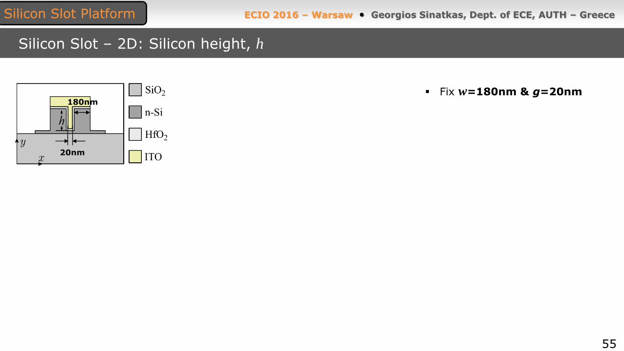
Silicon Slot – 2D: Silicon height, h
55
Silicon Slot Platform
Fix w=180nm & g=20nm 180nm
20nm
Page 56
ECIO 2016 – Warsaw • Georgios Sinatkas, Dept. of ECE, AUTH – Greece
Silicon Slot – 2D: Silicon height, h
56
2D Electrostatics
Silicon Slot Platform
180nm
20nm
Page 57
ECIO 2016 – Warsaw • Georgios Sinatkas, Dept. of ECE, AUTH – Greece
2D Eigenmode Solver
Silicon Slot – 2D: Silicon height, h
57
2D Electrostatics
Silicon Slot Platform
ER 1.10 dB/μm
IL 0.01 dB/μm
Increasing h values:
No impact on IL
Higher ER Shorter device lengths, L
Weak effect on energy consumption
Voff = 4V
h = 240nm
Minimal energy consumption
180nm
20nm
Page 58
ECIO 2016 – Warsaw • Georgios Sinatkas, Dept. of ECE, AUTH – Greece
Si-rib & Si-slot – Design & Performance Comparison
58
SOI Platforms
Page 59
ECIO 2016 – Warsaw • Georgios Sinatkas, Dept. of ECE, AUTH – Greece
Transparent Conducting Oxides
Tunable NIR properties by free-carrier concentration changes
Promising for applications in photonics (properties altering from dielectric to metallic)
ENZ effect in the NIR Electro-Optic modulators
Multiphysics Modeling Framework
Rigorous model developed instead of approximate techniques by integrating Solid-State physics and
Wave physics on a unified FEM platform
SOI-based TCO Electro-Optic Modulators
Si-rib Waveguide engineered for weak waveguiding (FoM not applicable)
TE-mode 0.30 (0.40) dB/μm ER & 0.03 dB/μm IL [0.11 & 0.045 dB/μm, Vasudev et al., Opt. Express, 2013]
TM-mode 0.25 (0.30) dB/μm ER & 0.02 dB/μm IL
Si-slot Waveguide engineered for strong waveguiding (FoM applicable)
Slot mode 1.10 (1.60) dB/μm ER & 0.01 dB/μm IL
What about bandwidth?
10% – 90% rise-time estimated around 2ps bandwidth exceeds 100GHz!
59
Summary & Conclusions
Page 60
ECIO 2016 – Warsaw • Georgios Sinatkas, Dept. of ECE, AUTH – Greece
60
Thank you!
[email protected]
http://photonics.ee.auth.gr
Page 61
http://photonics.ee.auth.gr
G. Sinatkas1, D. C. Zografopoulos2, A. Pitilakis1, R. Beccherelli2, E. E. Kriezis1
1Dept. of Electrical & Computer Engineering, Aristotle University of Thessaloniki, Greece
2Istituto per la Microelettronica e Microsistemi, Consiglio Nazionalle delle Ricerche (CNR-IMM), Rome, Italy
Transparent Conducting Oxide Electro-Optic Modulators:
A Comprehensive Study based on the Drift-Diffusion Semiconductor Model
Backup Material
Page 62
ECIO 2016 – Warsaw • Georgios Sinatkas, Dept. of ECE, AUTH – Greece
62
Temporal Response – Silicon Slot
tr ~ 2ps 10%
90%
Backup Material