1 Transparent Optical Switches: Technology Issues and Challenges G. Ellinas*, J. Labourdette*, J. Walker, S. Chaudhuri*, L. Lin, E. Goldstein, K. Bala* *Tellium Inc., 2 Crescent Place, Oceanport NJ 07757 1. Introduction Increased traffic volume due to the introduction of new broadband services is driving carriers to the deployment of an optical transport layer based on Wavelength Division Multiplexing (WDM) [1]. The network infrastructure of existing core networks is currently undergoing a transformation from rings using SONET Add/Drop Multiplexers (ADMs) to mesh topologies using Optical Cross-connects (OXCs). A core optical network architecture can be opaque or transparent. An opaque architecture means that the optical signal carrying traffic undergoes an Optical to Electronic to Optical (OEO) conversion at different places in the network. A transparent architecture means that the optical signal carrying traffic stays in the optical domain from the time it is generated at the edge of the network until it leaves the network. Even though the applications driving the large scale deployment of transparent optical switches are not currently in place (niche applications in today’s networks only use a very small number of transparent switches), and the traffic demand does not currently justify the use of transparent switches that are cost effective at very high bit rates, it is possible that at some point in the future transparent switches may be deployed in the network. Based on this assumption, this paper explores the technology issues and challenges that are associated with 3D MEMS-based switch fabrics. These fabrics offer the most viable approach to make single-stage switch fabrics with large port counts that can be used for the deployment of transparent switches in the network. Figure 1 illustrates the four different node architectures that can comprise a core optical network. The first architecture shows a fixed patch panel. Fixed patch panels located between WDM systems with transponders are currently being replaced by opaque (OEO) switching nodes (with electrical switch fabrics) as shown in architecture of Figure 1(b). This is an opaque network architecture, as the optical signal undergoes OEO conversions [2]. The third architecture shows a transparent (OOO) switch between WDM systems with transponders that is complemented by an OEO switch for drop traffic. This is once again an opaque network architecture, as the optical signal undergoes OEO conversions at the WDM
Transcript
1
Transparent Optical Switches: Technology Issues and Challenges
G. Ellinas*, J. Labourdette*, J. Walker, S. Chaudhuri*, L. Lin, E. Goldstein, K. Bala**Tellium Inc., 2 Crescent Place, Oceanport NJ 07757
1. Introduction
Increased traffic volume due to the introduction of new broadband services is driving carriers
to the deployment of an optical transport layer based on Wavelength Division Multiplexing
(WDM) [1]. The network infrastructure of existing core networks is currently undergoing a
transformation from rings using SONET Add/Drop Multiplexers (ADMs) to mesh topologies
using Optical Cross-connects (OXCs). A core optical network architecture can be opaque or
transparent. An opaque architecture means that the optical signal carrying traffic undergoes
an Optical to Electronic to Optical (OEO) conversion at different places in the network. A
transparent architecture means that the optical signal carrying traffic stays in the optical
domain from the time it is generated at the edge of the network until it leaves the network.
Even though the applications driving the large scale deployment of transparent optical
switches are not currently in place (niche applications in today’s networks only use a very
small number of transparent switches), and the traffic demand does not currently justify the
use of transparent switches that are cost effective at very high bit rates, it is possible that at
some point in the future transparent switches may be deployed in the network. Based on this
assumption, this paper explores the technology issues and challenges that are associated with
3D MEMS-based switch fabrics. These fabrics offer the most viable approach to make
single-stage switch fabrics with large port counts that can be used for the deployment of
transparent switches in the network.
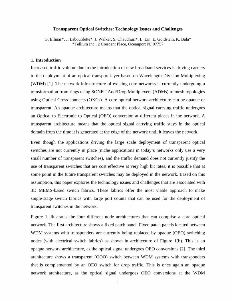
Figure 1 illustrates the four different node architectures that can comprise a core optical
network. The first architecture shows a fixed patch panel. Fixed patch panels located between
WDM systems with transponders are currently being replaced by opaque (OEO) switching
nodes (with electrical switch fabrics) as shown in architecture of Figure 1(b). This is an
opaque network architecture, as the optical signal undergoes OEO conversions [2]. The third
architecture shows a transparent (OOO) switch between WDM systems with transponders
that is complemented by an OEO switch for drop traffic. This is once again an opaque
network architecture, as the optical signal undergoes OEO conversions at the WDM
2
transponders. The fourth architecture shows a completely transparent network topology,
consisting of transparent optical switches and WDM systems that contain no transponders. In
such an architecture, the signal stays in the optical domain until it exits the network.
OpticalFabric Electronic Fabric
1(b) Opaque Network - Opaque Switch
OpticalFabric
1(c) Opaque Network - Transparent Switch
O/EO/E
Optical Fabric
1(d) Transparent Network - Transparent Switch
1(a) Opaque Network - Fixed Patch panel
Fixed PatchPanel
Figure 1: Node Architectures for a Core Optical Network
2. Transparent Network Architecture
The transparent network shown in Figure 1(d) and elaborated on in Figure 2 is a seemingly
attractive vision. A signal (wavelength) passing through an office does not undergo opto-
electronic conversion. Similarly, a client Network Element (NE), such as a router, interfaces
with the switch using long-haul optics to interface with the WDM equipment without any
O/E conversion. Since a signal from a client NE connected via a specific wavelength must
remain on the same wavelength when there is no wavelength conversion, only a small size
switch fabric is needed to interconnect the WDMs and NEs in a node. This architecture also
implies end-to-end bit rate and data format transparency. Note that another architecture of a
3
transparent switch in a transparent network may include a single large fabric instead of
multiple switch matrices of small port counts. If one is to provide flexibility, such an
architecture design would require the use of tunable lasers at the clients and wavelength
conversion.
Optical transport system
(1.5xx µm)...
...
Multiple transparentoptical switch matrices
......
... ...
Fixed ITU-grid 1.5xx µmlasers
Figure 2: Transparent switch architecture in a transparent network
This network may provide significant footprint and power savings and on the surface
suggests cost savings. However, while the transparent network architecture may be a viable
option for small-scale networks with pre-determined routes and limited numbers of nodes, it
is not a practical solution for a core network for the following reasons:
1. Based on the current state and history of research in the wavelength conversion arena,
it is highly unlikely that there will be field-deployable wavelength conversion
technology in the optical domain available in the next several years. In addition, for
this technology to be effective and in order to build a flexible network for unrestricted
routing and restoration capacity sharing, an all-optical 3R1 function must be available.
Even though a number of laboratory experiments have demonstrated all-optical 3R, a
commercial product that harnesses such a technology does not currently exist [3].
Such a network that does not allow for wavelength conversion is essentially a
network of n (n being the number of WDM channels) disjoint layers. Inflexible usage
4
of wavelengths in this network would lead to increased bandwidth and network
operational cost, thus negating the savings that may result from eliminating opto-
electronic conversion.
2. Physical impairments such as chromatic dispersion, polarization mode dispersion
systems, and packaging subsystems. The specifics and complexity of each of these
components depends dramatically upon the size and configuration of the cross-connect itself,
and presents significant challenges to the successful large-scale deployment of these network
elements.
(a) Optical Fiber Bundles
The optical signals to be switched by the optical cross-connect enter and exit the fabric via
two-dimensional arrays of optical fibers. The position of each fiber within each array must be
accurate in five dimensions, x, y, z, and both axes of tilt (see Figure 8). The required
translational accuracy of all fibers is measured in microns, with variant optical design choices
12
permitting no substantial relaxation of these requirements. Milliradian accuracy in fiber tilt is
required. Tolerances of this order place extremely high demands on fiber bundle
manufacturers. Thus far, capability has been demonstrated for low-volume supplies of fiber
bundles with fiber counts of a few hundred elements. The challenges faced in extending this
capability to 1,000+ fibers become more extreme as fiber handling and management issues
become more complex and the difficulty of achieving high yield arrays increases. The fiber
bundles are in general constructed using epoxy packing. These systems are currently
struggling to achieve the required positional accuracies with reasonable yield on day one;
aging properties over tens of years have not yet been seriously explored.
x
y
zθ
Figure 8: Fiber Bundles
(b) Lenslet Arrays
In order to achieve low loss through the switch fabric, collimation of the optical signals is
required. This is typically achieved through the use of 2D arrays of lenslets on the same pitch
as the optical fibers (see Figure 9). Various lenslet materials ranging from epoxies to glass,
silicon, and polymers are being explored. One of the chief technical hurdles is that of
achieving sufficiently tight variations in focal length. As with fiber arrays, the capability of
producing low volumes of arrays with hundreds of elements with sufficient yield has been
demonstrated; arrays of 1,000 or more lenslets are now at the frontier. At 1,000+ element
sizes, the present state of the component supply chain for both fiber arrays and lenslet arrays
13
can best be described as active research. It is expected, however, that volume availability will
be achieved in the next couple of years.
Figure 9: Lenslet Arrays
(c) MEMS Mirror Chips
The most common approach to providing beam steering functionality is to use 2D arrays of
gimbal-mounted 2-axis controllable mirrors. MEMS mirror chips have been developed using
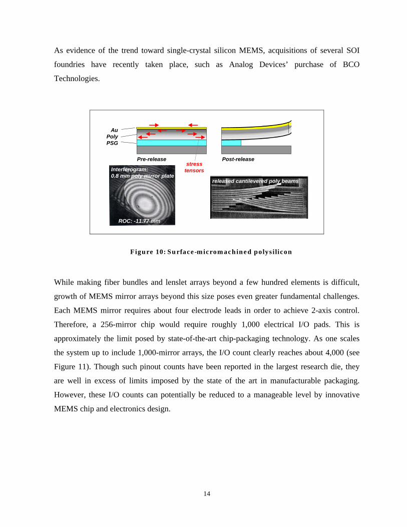
either polysilicon or single-crystal silicon (SCS) for the mirror structural material. Although
polysilicon is the technology with widespread use in MEMS systems for over ten years, it is
not well suited to optical MEMS applications due to inherent stress and stress gradient
through the material thickness. This stress and stress gradient typically cause curling of
released plates in polysilicon even in the absence of metalization that only becomes
exacerbated after deposition of mirror metals that have their own stress characteristics.
Finally, since polysilicon and metal films have different thermal expansion coefficients, the
amount of curling is thermally sensitive and very difficult to control over time and operating
conditions (see Figure 10). The curling contributes significant loss to the optical system
employing polysilicon mirrors. In recognition of the fact that polysilicon mirrors are highly
challenged to provide the extreme flatness required, on the order of 1 m radius of curvature,
the majority of switch fabric producers have moved toward single-crystal silicon as the
material of choice. Single-crystal silicon offers significant advantages over polysilicon for
optical MEMS technology due primarily to its very low inherent stress characteristics and
total lack of a stress gradient through the thickness of the material. Although it is a relatively
new material system to MEMS technologists, it is readily accessible through the use of well-
known silicon-on-insulator (SOI) technology and new deep reactive ion etching techniques.
14
As evidence of the trend toward single-crystal silicon MEMS, acquisitions of several SOI
foundries have recently taken place, such as Analog Devices’ purchase of BCO
Technologies.
stresstensors
Pre-release Post-release
released cantilevered poly beams
ROC: -11.77 mm
Interferogram:0.8 mm poly mirror plate
AuPolyPSG
Figure 10: Surface-micromachined polysilicon
While making fiber bundles and lenslet arrays beyond a few hundred elements is difficult,
growth of MEMS mirror arrays beyond this size poses even greater fundamental challenges.
Each MEMS mirror requires about four electrode leads in order to achieve 2-axis control.
Therefore, a 256-mirror chip would require roughly 1,000 electrical I/O pads. This is
approximately the limit posed by state-of-the-art chip-packaging technology. As one scales
the system up to include 1,000-mirror arrays, the I/O count clearly reaches about 4,000 (see
Figure 11). Though such pinout counts have been reported in the largest research die, they
are well in excess of limits imposed by the state of the art in manufacturable packaging.
However, these I/O counts can potentially be reduced to a manageable level by innovative
MEMS chip and electronics design.
15
Die package mockup
Figure 11: The electronic I/O bottleneck – Die package mockup
(d) MEMS Reliability
The entire MEMS field is relatively immature and therefore reliability concerns have only
recently begun to be addressed by the community at large. Reliability of MEMS devices has
been found to be exceptionally design-dependent with only some general cross-material
system characteristics. It is understood that reliability can be designed into a component by
avoiding operating characteristics such as surface contact, friction, and wear. MEMS designs
based on flexure elements have been shown to be orders of magnitude more reliable than
designs exhibiting these characteristics.
Since the predominant material system investigated to date has been polysilicon, much of the
reliability study has concentrated on polysilicon structures such as the Analog Devices’
ADXL50 accelerometer or Sandia National Lab’s gear/linkage systems. Unfortunately, while
polysilicon and single-crystal silicon have much in common, their reliability characteristics
are quite different. This fact has particular significance in the area of compliance testing,
because the time required for testing is commonly on the order of one year. The replacement
of a polysilicon element with a single-crystal silicon element will therefore require new and
equivalent testing and may delay deployment in commercial systems.
16
(e) Mirror Control
Because 3D MEMS switches couple single-mode fibers through free-space propagation
regions on the order of tens of cm, the demands that they place on control systems are quite
severe. The requirement for control is simple: upon execution of a switch command, place
two micromirrors, each with two angular degrees of freedom, in sub-milliradian alignment
within a few msec and hold this alignment through stochastic vibration, electronic
component variations, and temperature variations over twenty years with reliability suitable
for core-networking applications.
Four facts make this requirement particularly demanding. First, electrostatic MEMS actuators
are strongly nonlinear; thus, the control systems required are nonlinear. Second, because
making a connection requires the control of four angular variables, these nonlinear systems
must search and hold connection in a coupled four-dimensional space. Third, the micro-
electro-mechanics of MEMS structures result in large regions of electromechanical instability
in the operating space, while the need to restrain operating voltages generates strong
incentives to operate systems within these regions of instability. Finally, even after one has
devised a control system that overcomes the above challenges, such a system needs to know
in real time, with sub-milliradian accuracy, the angular position of each mirror in each of its
two orthogonal axes. This mirror position-sense system is in fact one of the more challenging
parts of a MEMS switch control system. To address this issue, substantial innovation in the
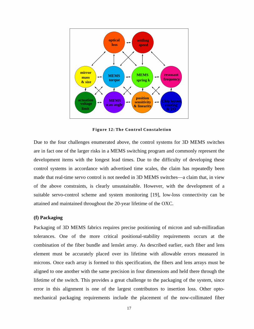
development of fundamentally new components and subsystems is required. Figure 12
shows the “control constaletion” that clearly demonstrates how a set of tightly-coupled
problems has to be resolved in order to address the control requirement.
17
settling speed
mirror mass & size
actuation voltage limit
position sensitivity
& linearityMEMS
scan angleChip layout,
routing & I/O
resonant frequency
MEMS torque
MEMS spring k
optical loss
Figure 12: The Control Constaletion
Due to the four challenges enumerated above, the control systems for 3D MEMS switches
are in fact one of the larger risks in a MEMS switching program and commonly represent the
development items with the longest lead times. Due to the difficulty of developing these
control systems in accordance with advertised time scales, the claim has repeatedly been
made that real-time servo control is not needed in 3D MEMS switches—a claim that, in view
of the above constraints, is clearly unsustainable. However, with the development of a
suitable servo-control scheme and system monitoring [19], low-loss connectivity can be
attained and maintained throughout the 20-year lifetime of the OXC.
(f) Packaging
Packaging of 3D MEMS fabrics requires precise positioning of micron and sub-milliradian
tolerances. One of the more critical positional-stability requirements occurs at the
combination of the fiber bundle and lenslet array. As described earlier, each fiber and lens
element must be accurately placed over its lifetime with allowable errors measured in
microns. Once each array is formed to this specification, the fibers and lens arrays must be
aligned to one another with the same precision in four dimensions and held there through the
lifetime of the switch. This provides a great challenge to the packaging of the system, since
error in this alignment is one of the largest contributors to insertion loss. Other opto-
mechanical packaging requirements include the placement of the now-collimated fiber
18
bundles with respect to the MEMS chips and holding these positions stable during ambient
temperature changes of tens of degrees Celsius. Finally, routing and management of
thousands of electrical cables and optical fibers into the switch bay in a compact and
organized manner is required [20].
5. Conclusion
The current state of affairs in terms of network deployment, applications and traffic demand
does not justify the large scale use of transparent switches in today’s networks. Some niche
applications do exist, but can mostly be addressed using a number of small transparent
switches. Provided that the traffic grows and the bit rates increase substantially there may
emerge a potential need for an additional network layer utilizing transparent optical switches.
Even from the technology standpoint, the present state of 3D MEMS-based switches is at
best “advanced development” for 256 port fabrics and “advanced research” for 1,000 port
fabrics. In the meantime, the deployment of transparent network elements is expected to
remain limited to wavelength selective cross-connect (WSXC) architectures and
Reconfigurable Optical Add Drop Multiplexers (ROADMs) on high capacity routes.
Furthermore, we anticipate that opaque switches will always remain for the embedded
service base even after the transparent switches are eventually introduced in the network.
These opaque switches will provide the grooming and multiplexing functions, as well as
some of the necessary control and management functions, and will scale and decrease in cost
with rapid progress in electronics.
References
1. T. Stern, K. Bala, Multiwavelength Optical Networks: A Layered Approach, Prentice Hall,May 1999.
2. K. Bala, et al, “The case for opaque multiwavelength lightwave networks”, IEEE/LEOSSummer Topical Meeting, 1995.
3. B. Mukherjee, “WDM Optical Communication Networks: Progress and Challenges”, IEEEJournal on Selected Areas in Communications, vol. 18, no. 10, pp. 1810-1824, October 2000.
4. B. Ramamurthy, et al, “Impact of transmission impairments on the teletraffic performance ofwavelength-routed optical networks,” IEEE/OSA J. Lightwave Technol., vol. 17, pp. 1713–1723, Oct. 1999.
5. C. S. Li et al., “Gain equalization in metropolitan and wide area optical networks usingoptical amplifiers,” in Proc. IEEE Infocom’94, Toronto, Canada, July 1994, pp. 130–137.
19
6. B. Ramamurthy, et al, “Optimizing amplifier placements in a multi-wavelength opticalLAN/MAN: The equally-powered-wavelengths case,” IEEE/OSA J. Lightwave Technol., vol.16, pp. 1560–1569, Sept. 1998.
7. B. Ramamurthy, et al, “Transparent vs. opaque vs. translucent wavelength-routed optical net-works,” in Proc. Optical Fiber Communications. (OFC’99), San Diego, CA, Feb. 1999,Paper TuF2, pp. 59–61.
8. G. Ellinas, et al, “Routing and Restoration Architectures in Mesh Optical Networks”, OpticalNetworks Magazine, Issue 4:1, January/February 2003.
9. J. Labourdette, et al, “Routing Strategies for Capacity-Efficient and Fast-Restorable MeshOptical Networks”, Photonic Network Communications, vol. 4, no. 3-4, pp. 219-235, 2002.
10. E. Bouillet, et al, “Addressing Transparency in DWDM Mesh Survivable Networks”, in Proc.OFC ’01, Anaheim, CA, March 2001.
11. J. Strand, A. Chiu, and R. Tkach: Issues for Routing in the Optical Layer, IEEECommunications Magazine, pp. 81-87, February 2001.
12. J. Walker, “The Future of MEMS in Telecommunication Networks”, J. Micromech.Microeng., Vol. 10, pp. R1-R7, 2000.
13. J. E. Ford and J. A. Walker, “Dynamic spectral power equalization using micro-mechanics,”IEEE Photonics Technol. Lett., vol. 10, pp. 1440-1442, 1998.
14. J. Ojha, “OIF Very Short Reach (VSR) Interface”, OIF White Paper, www.oiforum.com.15. L. Y. Lin, E. L. Goldstein, and R. W. Tkach, “Free-space micromachined optical switches
with submillisecond switching time for large-scale optical crossconnects,” IEEE PhotonicsTechnol. Lett., vol. 10, pp. 525-527, 1998.
16. R. T. Chen, H. Nguyen, and M. C. Wu, “A low voltage micromachined optical switch bystress-induced bending,” 12th IEEE International Conference on Micro Electro MechanicalSystems, Orlando, FL, 1999.
17. B. Behin, K. Y. Lau, and R. S. Muller, “Magnetically Actuated micromirrors for fiber-opticswitching,” Solid-State Sensor and Actuator Workshop, Hilton Head Island, SC, 1998.
18. H. Laor, “MEMS mirrors application in optical cross-connects,” IEEE LEOS Summer TopicalMeetings, Monterey, CA, 1998.
19. S. Pannu, C. Chang, R. S. Muller, and A. P. Pisano, “Closed-loop feedback-control systemfor improved tracking in magnetically actuated micromirrors,” International Conference onOptical MEMS, Kauai, Hawaii, Aug. 21-24, 2000.
20. R. Scotti, N. Basavanhally, Y. Low, D. Ramsey, and D. Bishop, “The Challenges ofPackaging MEMS Components for the All Optical Networks of the Future,” Design, Test,Integration, and Packaging of MEMS/MOEMS 2001, Cannes, France, pp. 19-27, 2001.