Trends And Skill Needs in the Field of Nanotechnology - The State of Affairs in the Czech Republic in the European Context Jan Voves Department of Microelectronics, Faculty of Electrical Engineering, Czech Technical University in Prague, Technická 2, 166 27 Prague 6, Czech Republic
Transcript
Trends And Skill Needs in the Field of Nanotechnology -
The State of Affairs in the Czech Republic in the European Context
Jan Voves
Department of Microelectronics, Faculty of Electrical Engineering,
Czech Technical University in Prague,Technická 2, 166 27 Prague 6, Czech Republic
emission. • spin-polarised field effect transistor (spin-
FET) - change properties of magnetic layer by applied gate voltage.
• spin resonant tunneling device (spin-RTD) • Multilayers with alternating magnetic and
non-magnetic semiconductors giantmagnetoresistance (GMR) effect - magnetic field sensors, hard disk industry.
• magnetoresistive random access memory(MRAM).
• quantum information processing– qubitsusing coherent spin states in quantum dots
Advantages of Spintronics
• nonvolatility, • increased data processing speed, • decreased electric power consumption, • increased integration densities compared with
conventional semiconductor devices.
Many of the difficulties and of the limits of candidate technologies for nanoelectronics and molecular electronics could be predicted, anticipated and, hopefully, solved if detailed modelling tools of realistic devices and structures were available.
• Process, device and circuit simulation modules
• Thermal and optical analysis as well.
• The semi-classical and quantum models are taken in the account.
Technology Computer Aided Design (TCAD)
Design loop
idea
simulation
ralization
experimentaltest
modiffication
specimentheoreticalsolution
simulation
time savings+
cost savings
Physical model levels
1nm 10nm 100nm 1000nm
electronwavelengthregion
electronfree-pathregion
localtermodynamicequilibriumregion
MICROPHYSICAL
QUANTUM
HYDRODYNAMIC
MACROPHYSICAL
critical dimensions
Nano-Characterisation Techniques
• Atomic Force Microscopy (AFM),• Scanning Tunneling Microscopy (STM)• Scanning Electron Miroscopy (SEM)
necessary for the correct implementation of physicalmodels into predictive simulation tools.
Nanotechnology Impacts• industry• health and society• ethical aspects• jobs• skill needs• education• training
GMR read heads Terabit memory and microprocessing
Single molecule DNA sizing and sequencing
Biomedical sensorsLow threshold lasersNanotubes for high
brightness displays
Nanodevices
Present Impact Potential Impact
N
S
Current cannot pass through
GMR
N
S
Thermal barriers Targeted drug deliveryInformation-recording layers Gene therapyOptical (visible and UV) barriers Multifunctional
8 nm gold particles attached to a 31 nm gold particle with DNA http://www.chem.nwu.edu/~mkngrp/dnasubgr.html
Nanotechnology Implications
• Nanotechnology will impact many technologies on short andlong term time frames
• Eventually nanotechnology will alter the way we make thingsand have the broad impact of the industrial or informationrevolutions
• New ways of making chemical and products may impactdistribution, consumption, energy use, environmentalcontamination. Potentially large impacts on the way we live.
• Rate of change and information growth is very rapid• The large impacts and rapid rate of change will likely cause
disruption of some type and fear
• Nanotechnology allow virtually total control of matter.
• Possible ethical issues includes non-therapeutic human enhancement
• Invasion of privacy due to invisible sensors.
• Much nanotechnology development is in the hands of private companies that are beyond direct public control.
• ‘nano-divide’ may arise between those countries or regions that understand the new technological approach and those that do not.
Impact on the Public Health, Safety and Environmental Protection
Nanoparticles have a greater reactive surface area per unit mass than larger particles, their toxicity and potential health effects may also increase.Inhaled particles couldinduce inflammation in the respiratorytract, causing tissue damage.
Ingested nanoparticles may cause liver damage: ingested nanoparticlesaccumulate in the liver, which couldeventually provoke excessive immuneresponses causing permanent liverdamage.
Health Riscs
All applications and use of nanotechnology must comply with the high level of public health, safety, consumers and workers protection, and environmental protection.
• Adequate transparency in research is essential, and a safe set of rules must be put in place.
• Public power, through politicians and public opinion, should therefore have the cultural instruments and access to appropriate qualified expertise to assess, steer and –where appropriate – constrain developments.
• Societal acceptance and confidence in nanotechnology
Impact on the Public Health, Safety and Environmental Protection
Two competing processes begin to affect jobs.
• boom time for jobs for the science and engineering workforce. need for supporting labour services, persons in sales, clerical and office work, service workers of different types.
• the technology reduces the number of workers needed to produce a given level of output.
Impact on the Jobs, Education and Training
Cost-reducing effect of nano
• nanotechnology lowers the cost of products, which increases demand for goods and expands jobs
• nanotechnology as a productivity enhancing technology
• improves real wages and living standards.
• generates additional consumer demand for all sorts of products and thus contribute to the growth of employment.
Skill needsWe need skilled people to produce the products and also to
use the products.• (more than 1 mil. researchers in Europe for
nanotechnology)• In Europe is lack of people with skills in business and
entrepreneurship
Needs:• Interdisciplinarity• Better communication skills• Team work skills
Interdisciplinarity• Nanoscience and nanotechnology are not one cohesive
discipline.
• Nanotechnology is composed of multiple disciplinesChemistry, physics, biology and information storage at theare linked at the nanoscale.
• Interdepartmental cooperation in making nanoscience and nanotechnologies course
• PhD´s with joint supervision from different disciplines
• Overcome institucional obstacles to interdisciplinary research
• Interdisciplinary nature of the work requires communication across technical and scientific fields, focusing on physics, chemistry, biology, toxicology and engineering, but also including entrepreneurial studies, risk assessment, and social and human sciences
• Each of the sciences and engineering represent distinct ways of seeing the natural world, with different jargon, culture, andanalytical tools.
• Nanotechnology workers must possess sufficient understanding of more than one discipline to promote efficient communication.
• Important to develop a common language that will permit an integrated exploration of nanotechnology.
Communication skills
Team Work
• Need local multi-disciplinary research centers• Best knowledge sharing - Scientific Hub• Frequent and informal interactions - Quick feedback loop• Best equipments sharing - Technological Hub • Brings complementary skilled scientists to Nano• Easy « bottom-up » - Self -assembly due to due to low
local barriers• Bottom-up = motivation + confidence = creativityProject /
team - based learning• New research organization - Multi-disciplinary teams in a
fractal network• International cooperation
• Many scientifically trained graduates have left scientific fields in favour of positions in finance, management or other non-science related jobs.
• Many students have become disillusioned with the sciences as a career option.
• Nanoscience and nanotechnology are very attractive
• Hope that some will prefer nano-fun to law-money
• Working on on nanotech problems involving backgroundknowledges
Recruitment
Nanotechnology EducationMore than one type of education is needed needed:• Experts – research, engineering, manufacturing, policy,
safety and regulation• Workforce skills need to be identified and taught (clean
room skills, computer skills...)• Need deeper understanding of characterization tools and
metrology for manufacturing and commerce• Need terminology appropriate for education, regulation
and manufacturing• Need to facilitate formation of creative multi-disciplinary
teams• Not technical skills – social issues, ethic, philosophy,
safety, health, environment, communication
Long Term Education Needs• Primary and secondary - Nanoscience information
integrated into course structures. Development ofconcepts and language.
• Terciary – Specific courses in nanoscience andintegration of nanoscience into other science and mathcourses.
• Graduate – Combine knowledge depth in at least oneskill area with skills to participate in and lead multi-disciplinary teams.
• Lifelong education – With the rapid knowledge growth,education is a continual process
Primary and secondary schools
• To stimulate future interest for the intellectual challenges of science and research, observation, analysis, interpretation, abstraction and prediction skills have to be developed in primary and secondary schools
• Contact with science is essential at early ages - primaryschool (5-12)
• Initiate to scientific reasoning• Demonstrate simple phenomenon - « fun » science • Use nano-fascination to attract students - Science is alive
and fascinating• Visit the labs
• Conceptual and language barriers prohibit fruitfulcollaborations collaborations _
• Background education in all important disciplines fornanotechnology Physics, biology, chemistry, engineering
• All aspects including ethics and societal impact• Nanooriented courses• Nano science, nanofabrication, nano characterisation• Specific nano Diploma• Potentially attractive for students• Opportunity: The new bachelor -master system
Tertiary Education System
A distinction should be made between first (bachelors) and postgraduate degrees in nanotechnology.
• It is still unknown whether a three of four year taught course at the first degree level will allow students to gain the required level of expertise in any discipline to be useful to future employers
• would be better to have a sound understanding of one area of science first and then broaden this to include other disciplines.
postgraduate courses• specifically designed to give multidisciplinary skills. • adding elements of entrepreneurship or business skills
Tertiary Education System
Career re-orientation and follow-up are are essential in a rapidly changing technology
• important opportunity for university-industrycollaborations
• reorientation courses, summer schools, and workshops
• mid-career post-doctorates • international co-operation
Continuous Training
Public Education
• Awareness of potential risk should also include potential benefits of nanotech
• Information to broader public is indispensable in order to ensure an informed dialogue
• Avoid exaggerating the technological potential and respond to irrational fears
• Educated politicians, more scientists in policy decision positions
• Societal acceptance and confidence in nanotechnology
Basic research remains the essential element to technical infrastructure. • Knowledge flows primarily from academic labs to industry.• Industry do not readily profit from investing in basic science
(no commercial value in any reasonable time period)• Temptation to allow industry to control it or to dictate the
direction of academic research • Reduce the government’s burden for funding academic
science.
dangerous strategy - firms have a strong incentive to restrict the knowledge that they help to create, which would result in a slowdown of the overall pace of basic research.
Basic Research
European and CzechNano-Infrastructure
• poles of exelence• education• institutes
Communication Towards a European Strategy for Nanotechnology adopted by EC Commission in 2004
• Research and development infrastructure system of comprises ‘single sited’ (in one location) and ‘distributed’ (networked) facilities.
• nanotechnology requires a critical mass of resourcesthat are beyond the means of regional and often even national governments and industry.
• Poles-of excellence can bring together faculty members of different disciplines under a single organization
• these researchers may retain a desk at their ‘home’department.
Poles of Excellence
Special attention will be paid to the needs of industry.
• Small and medium sized enterprises (SMEs) reinforce cooperation and technology transfer from academic teams to conceive advanced prototypes and validate them in industrially relevant environments.
• SMEs and regional technological clusters integrating industry, research institutes and universities can play a crucial role in particular at regional level.
• ‘Regions of Knowledge’ initiative could contribute towards establishing effective clusters and networks.
Regions of Knowledge
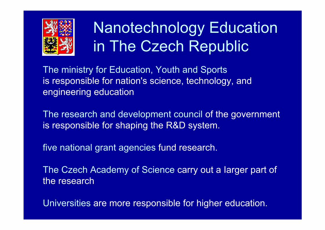
The ministry for Education, Youth and Sportsis responsible for nation's science, technology, and engineering education
The research and development council of the government is responsible for shaping the R&D system.
five national grant agencies fund research.
The Czech Academy of Science carry out a Iarger part of the research
Universities are more responsible for higher education.
Nanotechnology Education in The Czech Republic
• approved by the Czech government in April 2003• for the period from 2004 to 2009 • consists of five thematic programs • program No.3 "Competitiveness in Sustainable Developmenť' • six sub-programs
• the sub-program "Manufacturing Processes and Systems" key research direction "Electronic and Photonic Materials and Structures", also focuses on Nano-Electro-Mechanical-Systems (NEMS), molecular electronics, new carbon and bio-mimetic materials.
• the sub-program "Emerging Technologies" includes the key research direction "Nanotechnologies and Nanomaterials"
National Research Program
To realize the mentioned potential of nanotechnology research, the Czech Republic needs a population of interdisciplinary researchers and engineers who can generate knowledge and ensure that this is, in turn, transferred to industry. To meet the need of the nanotechnology infrastructure of research and education at the national and international level, new and existing nanotechnology networks are developed and shared. A hierarchal infrastructure has recently been completed.
Nanotechnology Infrastructure
Centre NANOTECH CTU
• was established in 2004 • workgroup for micro- and nanotechnology of the
Czech Technical University
• continuous communication between teams of different but complementary research profiles
• results in advances for future application of nanotechnologies
• improved education in nanotechnology, especially in the PhD study programs
University Level
The Czech Society of New Materials and Technologieswas founded in 2002 its "Nanoscience and Nanotechnology Section" with more than 100 members with several working groups
the working group Educationorganizes the network of Czech universities with the aim:• to build up the infrastructure for experience exchange• to establish new courses and curricula in the field of nanotechnology• to encourage the collaboration with the Czech Academy of Science
coordination role in the process of implementation.
National Level
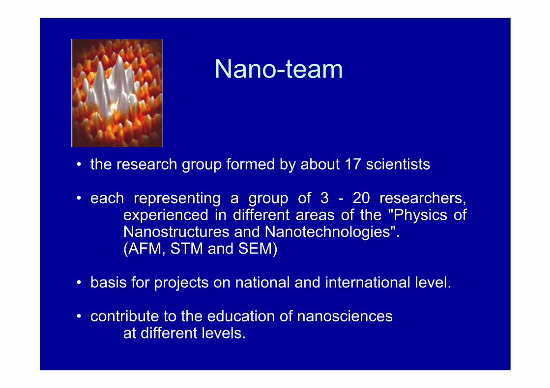
Nano-team
• the research group formed by about 17 scientists
• each representing a group of 3 - 20 researchers,experienced in different areas of the "Physics of Nanostructures and Nanotechnologies". (AFM, STM and SEM)
• basis for projects on national and international level.
• contribute to the education of nanosciencesat different levels.
Institute of Applied Sciences
All groups in this region are cooperating in preparation of a new Institute of Applied Sciences - IAS.
There are four main proposed research areas in IAS:• nanosciences, • special chemistry, • new energy sources • applied mathematics.
Institute will concentrate expensive equipments for the electron lithography and nano characterisation techniques.
Mainly PhD students will take part in the IAS research.
It could be be a new "pole of excellence".
Network for Nanostructured Materials - NENAMAT
• proposed by 10 Centres of Associate Candidate Countries(the Czech coordinator in the Technical University in Brno)
• founded in 2004 • to improve the knowledge base of application-oriented
nanosciences and technology • to help in building of the European nanotechnology related
industry.
European Level
Network MNT ERA-NET (Micro- and Nanotechnology European Research Area Network)
• integrates nanotechnology programs of new participants into the already existing network.
• The Czech Republic is planned to be included as an associated member.
The planned activities include • the systematic exchange of information about programs, • implementation of joint activities, co-operation programs,
transnational research activities, and the institutionalization of co-operation.
European Level
"International Dialogue on Responsible Research and Development of Nanotechnology"
• global group of experts involved with nanotechnology from 25 countries
• met in 2004 in USA.
• The NSF USA, EU and Japan will continue to organize future meetings of the expanded group.
• The Czech Republic has been nominated into the group, which is responsible for conceptual education for nanotechnology .
Global level
Currently there is no specific state program supporting the related research and development and no specific study program focusing on nanotechnology (or curricula, specialization or course) at Czech Technical Universities. Nanoscience and nanotechnology are only partially included in courses like physics, chemistry, physical chemistry, electronics, materials engineering, etc.
Czech Universities
PLD
SKA
PRAHACzech Technical Univ.Charles´ UniversityU. of Chem. Technology
CESKE BUDEJOVICESouth Bohemia Univ. BRNO
Masaryk UniversityTechnical Univ.
LIBERECTechnical Univ.
PLZENWest Bohemia Univ.
USTI nad LabemJ.E.Purkyne Univ.
OSTRAVATechnical Univ.
ZLINT. Bata Univ.
OLOMOUCPalacky Univ.
PARDUBICEUniversity
Czech Universities
Czech Technical University in Prague: Diagnostics of nanomaterials, nanoelectronics, subnanometric InAs/GaAs laser structures, nanostructural coatings, biomedical engineering, biocybernetics, low-dimensional semiconducting structures, self-assembly of carbon colloids, nanocrystalline diamond like layers, microalloyed steels, polymeric nanocomposite materials. Nanotechnology is included in the education as well in these subjects: New trends in Electronics. Electronics of Semiconductors, TCAD for Electronics and in the new subject Nanotechnology at the Department of Microelectronics and the Department of Mechanics andMaterial Science, Faculty of Electrical Engineering CTU.
Charles University in Prague: II-VI and III-V semiconductor based nanostructures. Nucleation and growth of metals on Si for nanoelectronics. Nanotechnology is included in the MSc. course in Chemistry at the Faculty of Science.
University of Chemical Technology in Prague: Chemical and structural analysis, submicron polymeric films with high permitivity, diffusion in nanometric scale.
Czech Universities
Technical University in Brno: Nanolithography by SPM. Nano-structured thin layers, functional gradient materials, nano-structured ceramics, AFM, near field optical microscopy .
Masaryk University in Brno:Low-dimensional semiconducting structures, plasma-chemical deposition, structure and function of biomolecules and proteins, processing of fullerens and nanotubes, diagnostics of nanomaterials, near-field optical microscopy, AFM, magnetic-force microscopy. Nanostructures in III-V semiconductors and cuprates/manganites.
Tomas Bata University in Zlin:Nanotechnolgy is included in the M.Sc. course Material Science
Palacky University Olomouc:Nanocomposite and nanobiotechnology. Amorphous and nanocrystalline iron oxides.
Czech Universities
Technical University in Ostrava: Periodic nanostructures, magneto-optics, layered nanostructures, nanoparticles and nanocomposites, clay-polymer, anticorrosion layers.
West Bohemia University in Plzen: Thin and hard layers. Nanotechnolgy is included in the M.Sc. course Applied Science.
South Bohemia University in Ceske Budejovice: Nanoparticles in biosciences.
J. E. Purkyne University in Usti nad Labem: SnO2 thin films and nanometer surface analysis.
Technical University in Liberec: Nanofibers.
University in Pardubice: Amorphous chalkogenides.
Czech Universities
Institute of Physics in Prague: Quantum size MOVPE grown AIIIBV nanostructures. Nano/micro-crystalline Si and Sinanocrystals. Nano-phenomena on metal interfaces. Dielectric properties of nano-inhomogeneities in condensed matter. MBE AIIIBV nanostructures and diluted magnetic semiconductors.
Institute of Radio Engineering and Electronics in Prague: Nano-porous AIIIBV structures.
Institute of Scientific Instruments in Brno: Diagnostics of nanostructures with very low energy electrons.
Research Institutes
Institute of Macromolecular Chemistry Prague:Macromolecular assemblies, bioanalogous polymers, synthetic drug and gene carriers. Polymeric quantum dots, molecular wires and switches,, structure and preparation of polypeptide systems, self-assembly, biocompatible interfaces. Polymer-based luminescent complexes.
J. Heyrovsky Institute of Physical Chemistry in Prague: Nanostructured Carbon Allotropes and their Derivatives.
Institute of Inorganic Chemistry in Řež near Prague: Nanocomposites with controlled size of nanoparticles, nanostructures for optoelectronics.
Institute of Experimental Technology in Prague: Quantum light generators.
Instituteof Microbiology in Prague: Nanobiotechnology.Institute of Biophysics in Prague: Study of DNA and proteins.Institute of Organic Chemistry and Biochemistry in Prague: Study of proteins.
Research Institutes
Conclusions• Interdisciplinary research and education is the most important aspect in
nanotechnology. • Universities should introduce courses based on nanoscale science and
integrate nanotechnology with physics, chemistry, biology, electronics, medicine, engineering and other fields.
• To meet the needs of the research and education in nanotechnology the infrastructure at the national and international level has recently been formed.
• Poles of exelence will play a central role in the development of the society of knowledge needed for the nanotechnology.
• International collaboration and academy-industry cooperation is necessary.
• Because of the fact that manufacturing at the nanoscale has potential to decrease the consumption of energy, water, materials, waste, contaminants and because some nanotechnologies include also serious potential risks, nanotechnology education must also include environmental, health, ethical, and legal aspects.