25
Trends in Test Technology for Advanced Packaging Joe Klein Region Sales Manager TEL Test Systems
Trends in Test Technology for Advanced PackagingJoe Klein Region Sales Manager TEL Test Systems
Die Level test system / TEL / ATSBU, TS-Dept. / Rev.0 / 2015 Jan 12th
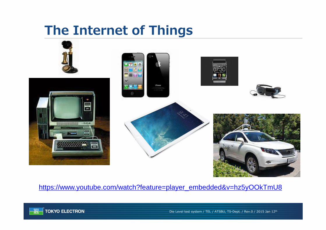
The Internet of Things
https://www.youtube.com/watch?feature=player_embedded&v=hz5yOOkTmU8
Die Level test system / TEL / ATSBU, TS-Dept. / Rev.0 / 2015 Jan 12th
Honey, I Shrunk the Package?
Die Level test system / TEL / ATSBU, TS-Dept. / Rev.0 / 2015 Jan 12th
Die Level test system / TEL / ATSBU, TS-Dept. / Rev.0 / 2015 Jan 12th
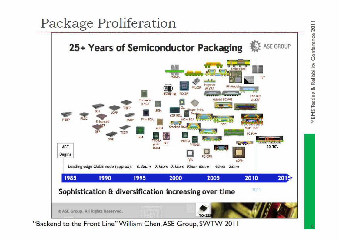
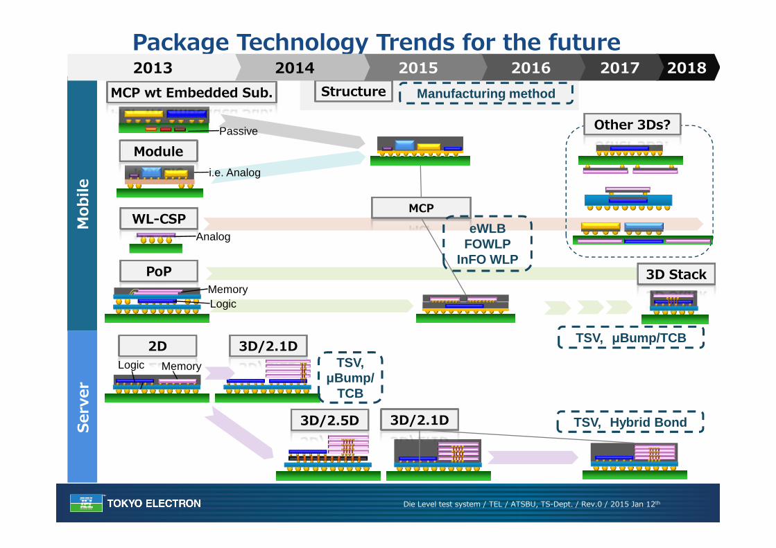
Package Technology Trends for the future
3D/2.5D
3D/2.1D
PoP
Mob
ileSe
rver
WL-CSP
3D/2.1D
Logic
i.e. Analog
Module
Memory
MCP
TSV,µBump/
TCB
TSV, Hybrid Bond
eWLBFOWLP
InFO WLP
Structure Manufacturing method
Analog
MCP wt Embedded Sub.
Passive
3D Stack
TSV, µBump/TCB
Other 3Ds?
2DLogic Memory
201820172016201520142013
Die Level test system / TEL / ATSBU, TS-Dept. / Rev.0 / 2015 Jan 12th
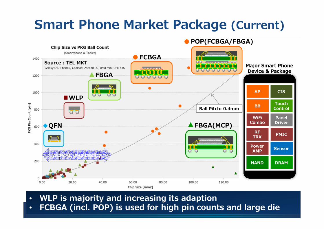
Smart Phone Market Package (Current)
TouchControl
RFTRX
BB
CISAP
PanelDriver
WiFiCombo
PMIC
NAND DRAM
PowerAMP Sensor
WLP
QFN
FBGA
POP(FCBGA/FBGA)
FBGA(MCP)
Ball Pitch: 0.4mm
FCBGAMajor Smart PhoneDevice & Package
Galaxy S4, iPhone5, Coolpad, Ascend D2, iPad min, UMI X1SSource : TEL MKT
WLP(FI) Availability
• WLP is majority and increasing its adaption• FCBGA (incl. POP) is used for high pin counts and large die
Die Level test system / TEL / ATSBU, TS-Dept. / Rev.0 / 2015 Jan 12th
7
Die Level test system / TEL / ATSBU, TS-Dept. / Rev.0 / 2015 Jan 12th
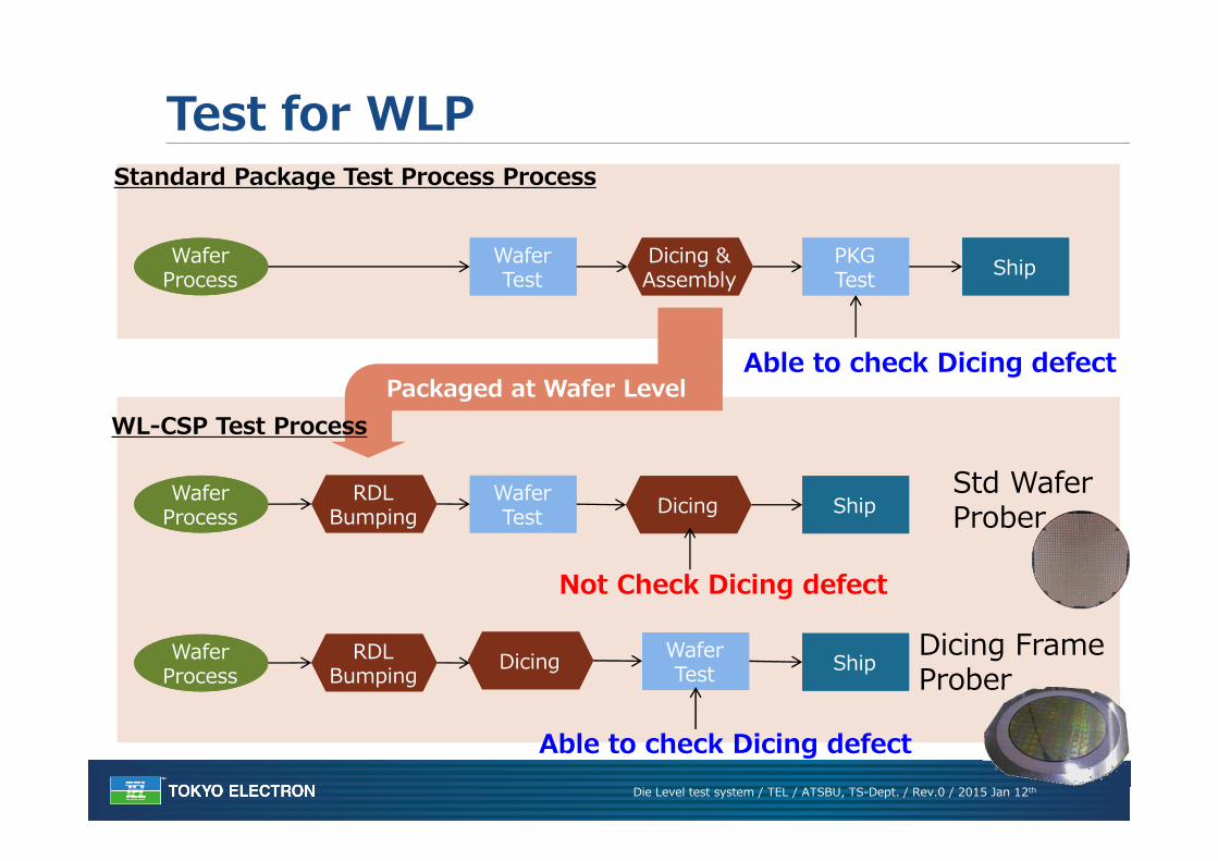
Wafer Test
Wafer Test
Wafer ProcessWafer
Process
Test for WLP
WaferProcessWafer
ProcessWafer Test
Wafer Test
Dicing &AssemblyDicing &Assembly ShipShipPKG
TestPKGTest
Standard Package Test Process Process
WL-CSP Test ProcessPackaged at Wafer Level
RDLBumping
RDLBumping DicingDicing ShipShip
Wafer ProcessWafer
ProcessRDL
BumpingRDL
Bumping ShipShipWafer Test
Wafer TestDicingDicing
Not Check Dicing defect
Able to check Dicing defect
Dicing Frame Prober
Std Wafer Prober
Able to check Dicing defect
Die Level test system / TEL / ATSBU, TS-Dept. / Rev.0 / 2015 Jan 12th
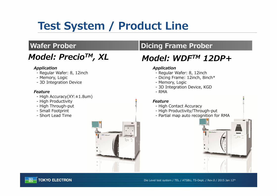
Test System / Product LineWafer Prober Dicing Frame ProberModel: PrecioTM, XL Model: WDFTM 12DP+
Application- Regular Wafer: 8, 12inch- Memory, Logic- 3D Integration Device
Feature- High Accuracy(XY:±1.8um)- High Productivity- High Through-put- Small Footprint- Short Lead Time
Application- Regular Wafer: 8, 12inch- Dicing Frame: 12inch, 8inch*- Memory, Logic- 3D Integration Device, KGD- RMA
Feature- High Contact Accuracy- High Productivity/Through-put- Partial map auto recognition for RMA
Tutorial on Frame Probing
Die Level test system / TEL / ATSBU, TS-Dept. / Rev.0 / 2015 Jan 12th
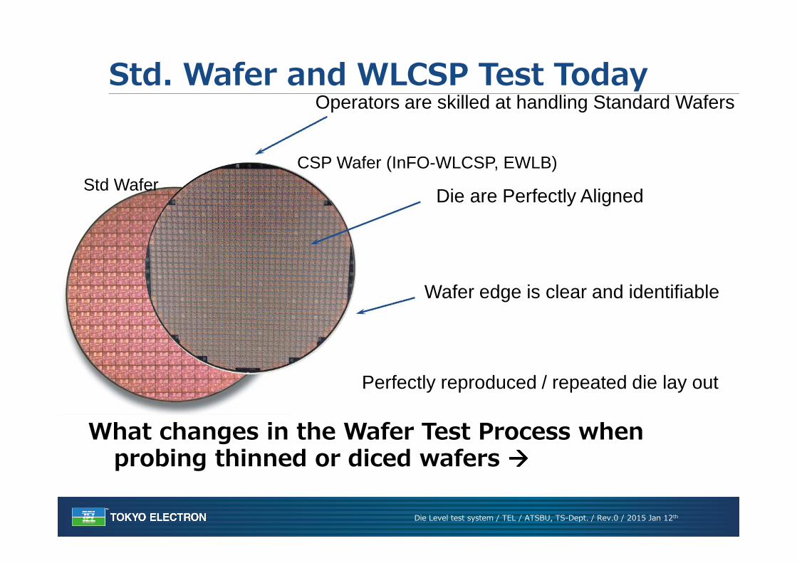
Std. Wafer and WLCSP Test Today
What changes in the Wafer Test Process when probing thinned or diced wafers ����
Operators are skilled at handling Standard Wafers
Wafer edge is clear and identifiable
Perfectly reproduced / repeated die lay out
Die are Perfectly Aligned Std Wafer
CSP Wafer (InFO-WLCSP, EWLB)
Die Level test system / TEL / ATSBU, TS-Dept. / Rev.0 / 2015 Jan 12th
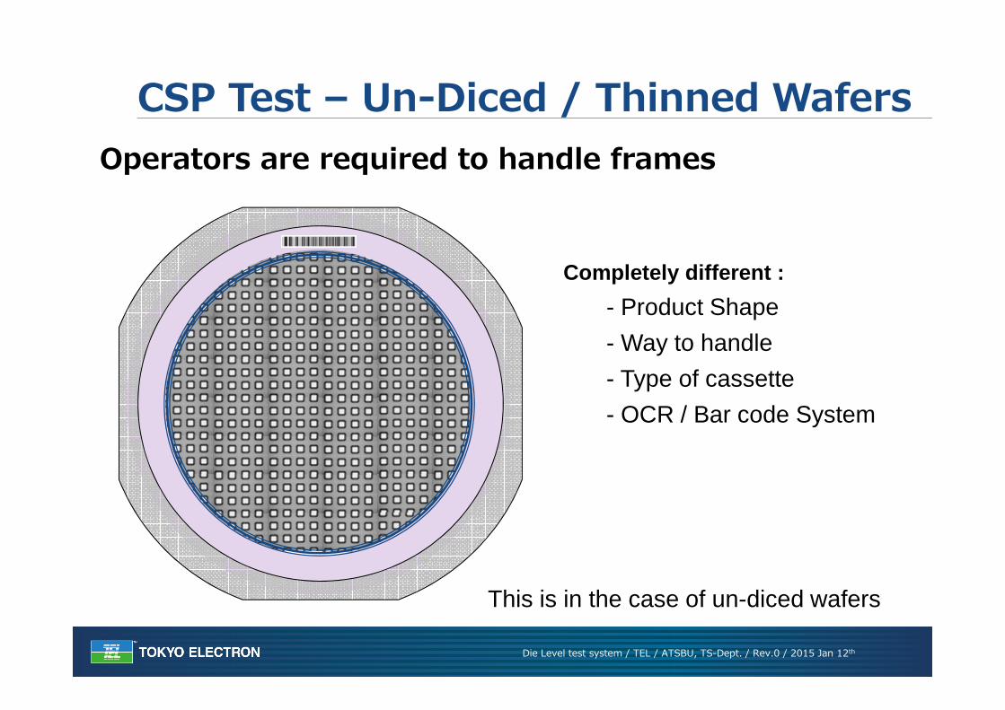
CSP Test – Un-Diced / Thinned WafersOperators are required to handle frames
Completely different :
- Product Shape
- Way to handle
- Type of cassette
- OCR / Bar code System
This is in the case of un-diced wafers
Die Level test system / TEL / ATSBU, TS-Dept. / Rev.0 / 2015 Jan 12th
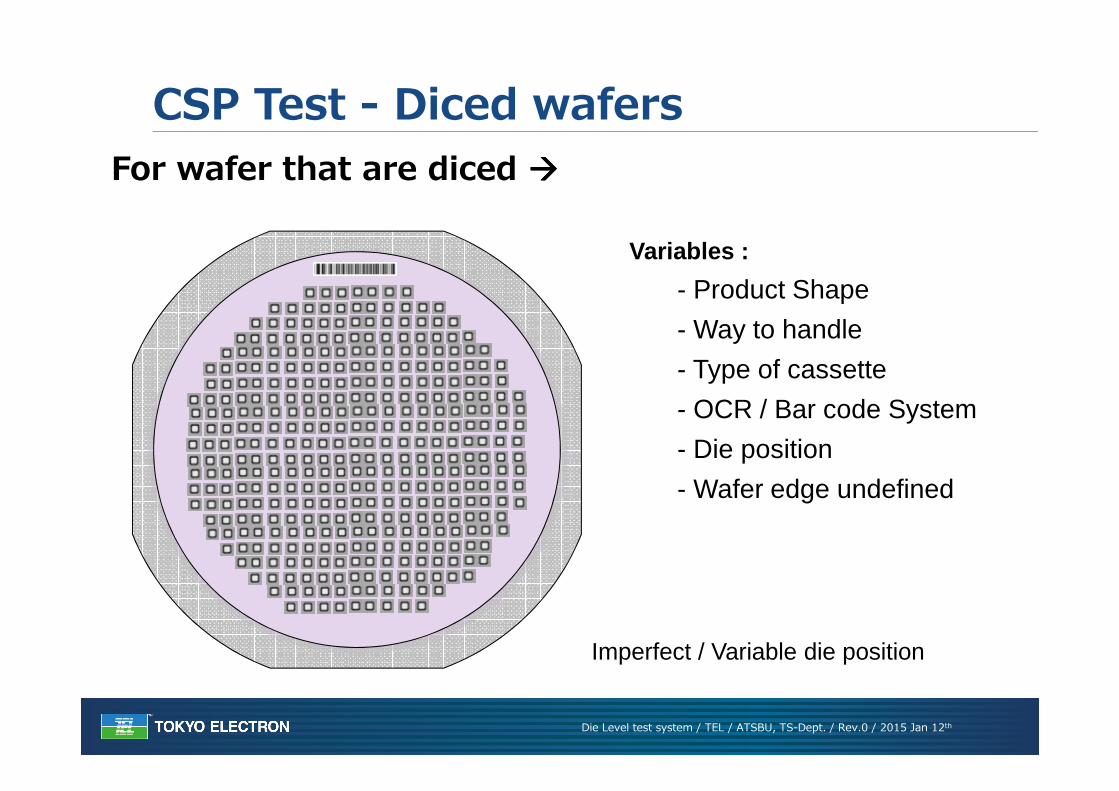
CSP Test - Diced wafersFor wafer that are diced ����
Variables :
- Product Shape
- Way to handle
- Type of cassette
- OCR / Bar code System
- Die position
- Wafer edge undefined
Imperfect / Variable die position
Die Level test system / TEL / ATSBU, TS-Dept. / Rev.0 / 2015 Jan 12th
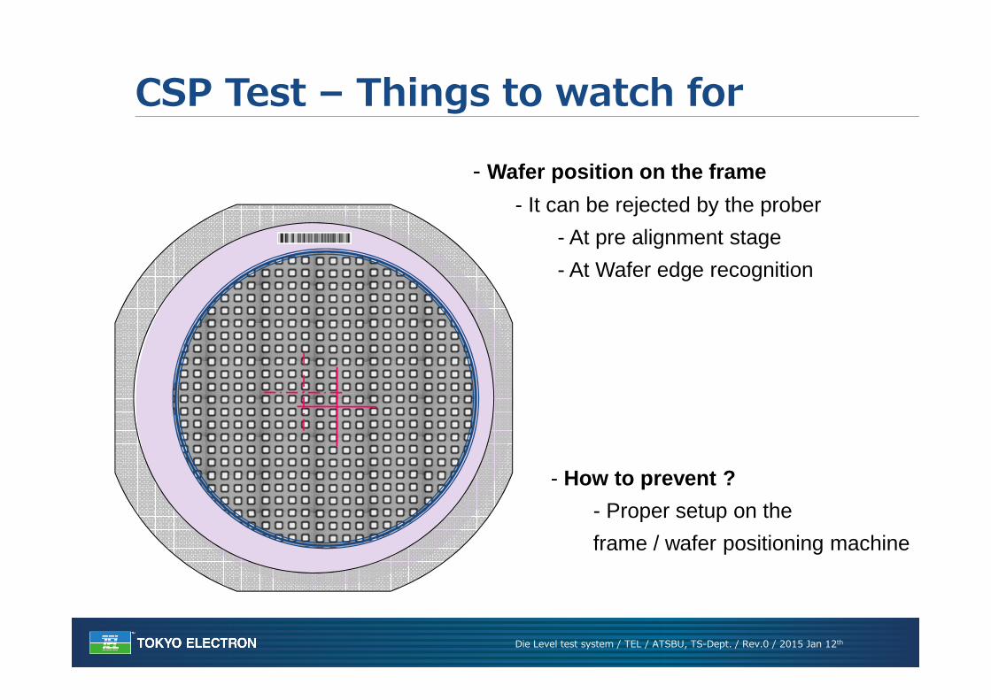
CSP Test – Things to watch for
- Wafer position on the frame
- It can be rejected by the prober
- At pre alignment stage
- At Wafer edge recognition
- How to prevent ?
- Proper setup on the
frame / wafer positioning machine
Die Level test system / TEL / ATSBU, TS-Dept. / Rev.0 / 2015 Jan 12th
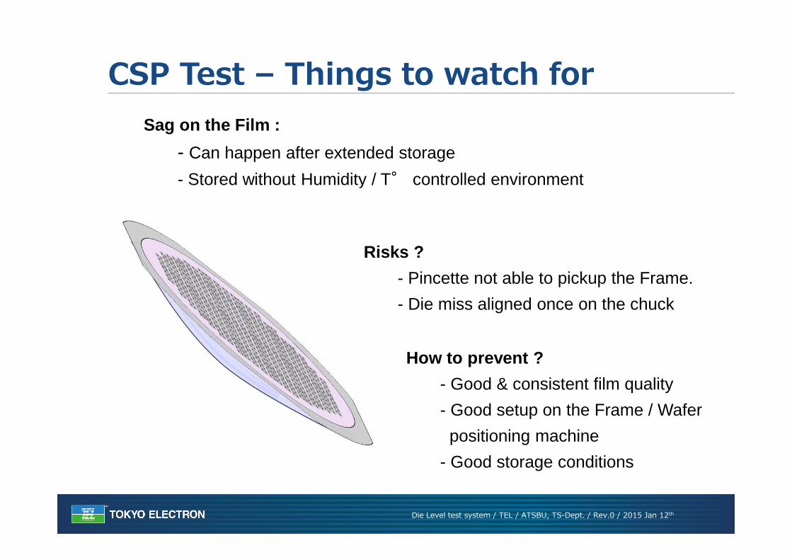
Sag on the Film :
- Can happen after extended storage
- Stored without Humidity / T° controlled environment
CSP Test – Things to watch for
How to prevent ?
- Good & consistent film quality
- Good setup on the Frame / Wafer
positioning machine
- Good storage conditions
Risks ?
- Pincette not able to pickup the Frame.
- Die miss aligned once on the chuck
Die Level test system / TEL / ATSBU, TS-Dept. / Rev.0 / 2015 Jan 12th
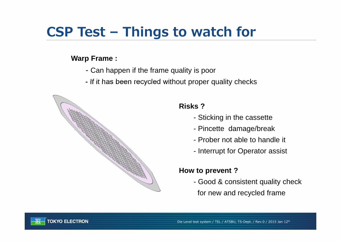
Warp Frame :
- Can happen if the frame quality is poor
- If it has been recycled without proper quality checks
CSP Test – Things to watch for
How to prevent ?
- Good & consistent quality check
for new and recycled frame
Risks ?
- Sticking in the cassette
- Pincette damage/break
- Prober not able to handle it
- Interrupt for Operator assist
Die Level test system / TEL / ATSBU, TS-Dept. / Rev.0 / 2015 Jan 12th
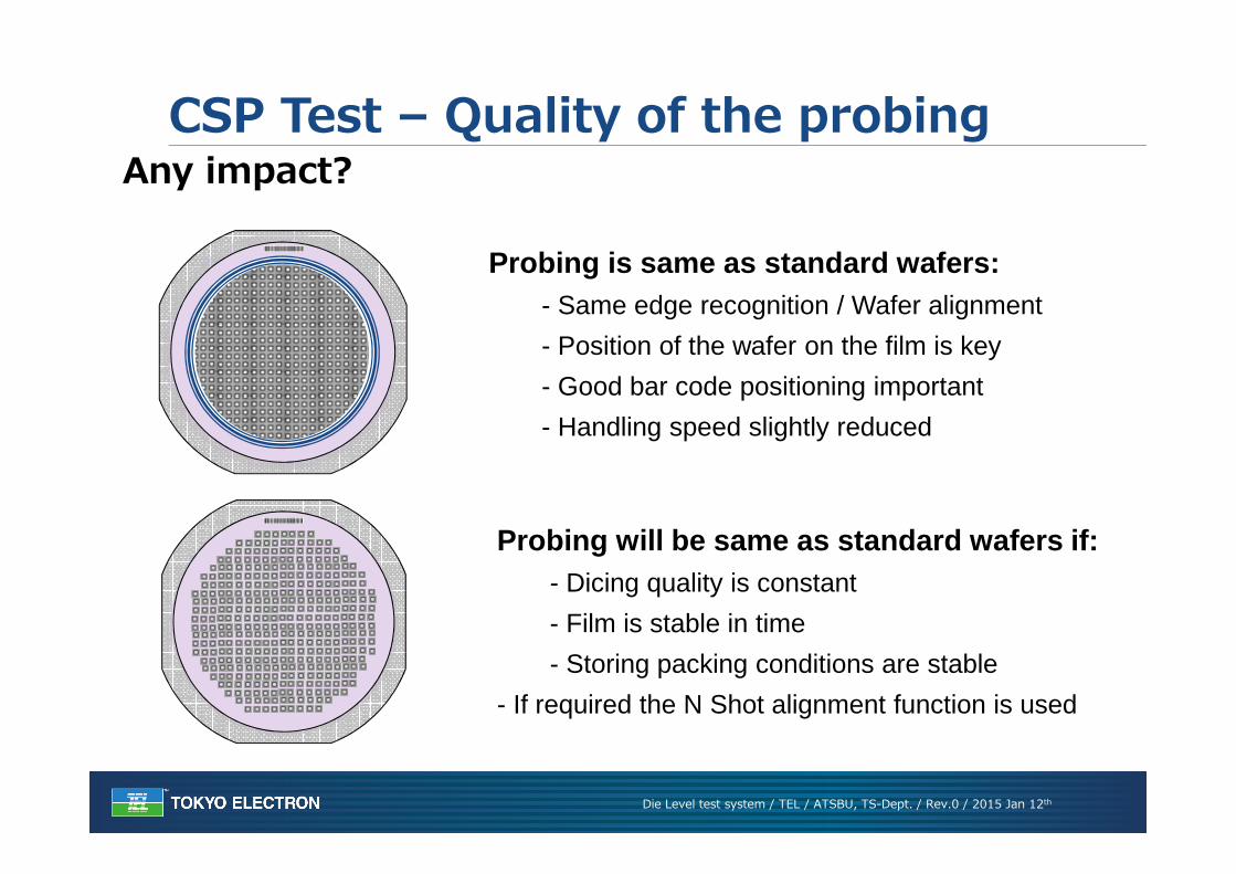
CSP Test – Quality of the probingAny impact?
Probing is same as standard wafers:- Same edge recognition / Wafer alignment
- Position of the wafer on the film is key
- Good bar code positioning important
- Handling speed slightly reduced
Probing will be same as standard wafers if:- Dicing quality is constant
- Film is stable in time
- Storing packing conditions are stable
- If required the N Shot alignment function is used
CONFIDENTIAL
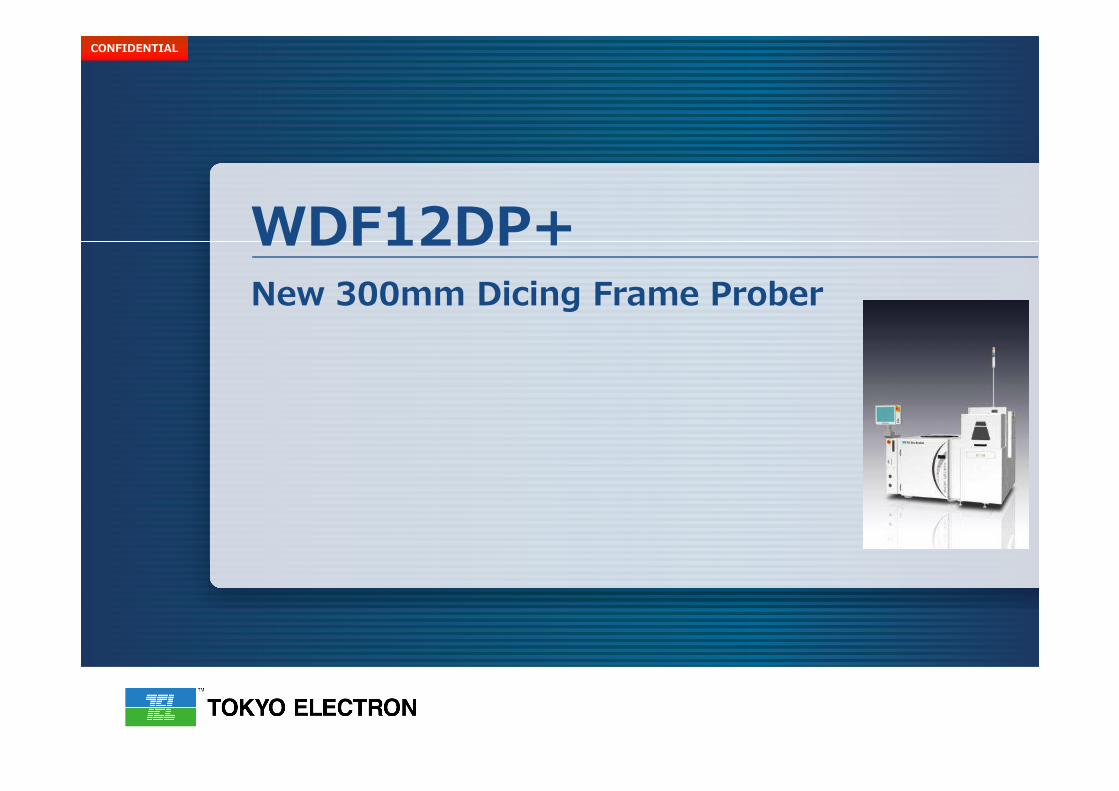
WDF12DP+New 300mm Dicing Frame Prober
Die Level test system / TEL / ATSBU, TS-Dept. / Rev.0 / 2015 Jan 12th
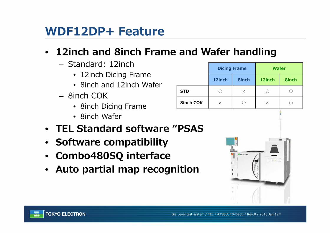
WDF12DP+ Feature• 12inch and 8inch Frame and Wafer handling
– Standard: 12inch• 12inch Dicing Frame• 8inch and 12inch Wafer
– 8inch COK• 8inch Dicing Frame• 8inch Wafer
• TEL Standard software “PSAS• Software compatibility• Combo480SQ interface• Auto partial map recognition
Dicing Frame Wafer
12inch 8inch 12inch 8inch
STD ○ × ○ ○
8inch COK × ○ × ○
Die Level test system / TEL / ATSBU, TS-Dept. / Rev.0 / 2015 Jan 12th
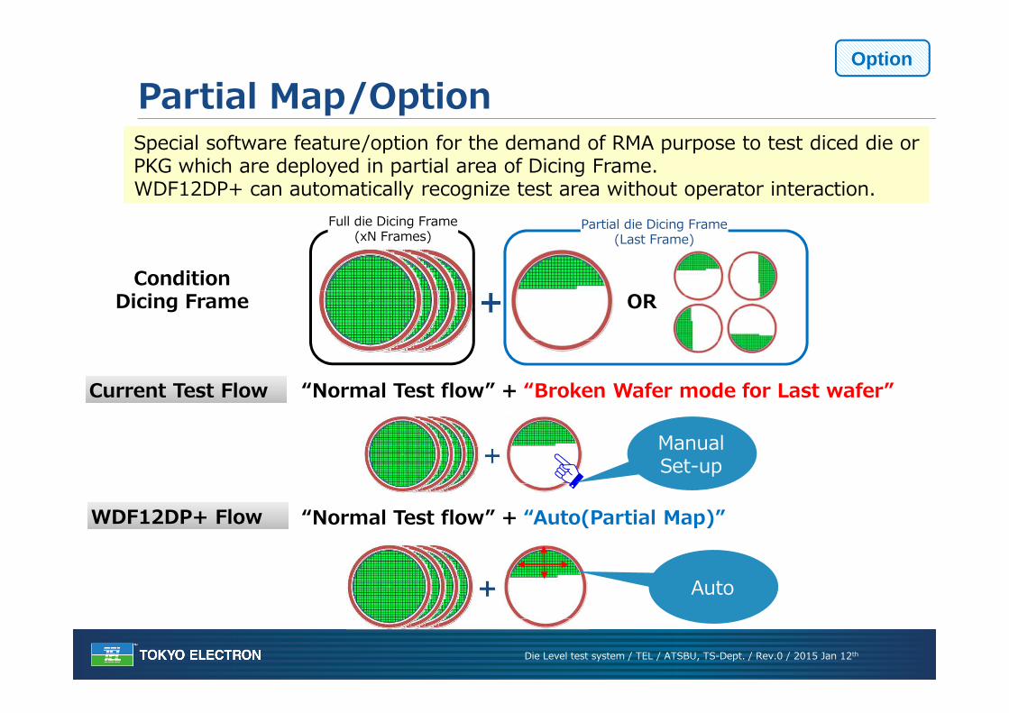
Partial Map/OptionSpecial software feature/option for the demand of RMA purpose to test diced die or PKG which are deployed in partial area of Dicing Frame.WDF12DP+ can automatically recognize test area without operator interaction.
“Normal Test flow” + “Broken Wafer mode for Last wafer”Current Test FlowCurrent Test Flow
WDF12DP+ FlowWDF12DP+ Flow “Normal Test flow” + “Auto(Partial Map)”
Manual Set-up
Auto
ORCondition
Dicing Frame
Full die Dicing Frame(xN Frames)
Partial die Dicing Frame(Last Frame)
Option
Die Level test system / TEL / ATSBU, TS-Dept. / Rev.0 / 2015 Jan 12th
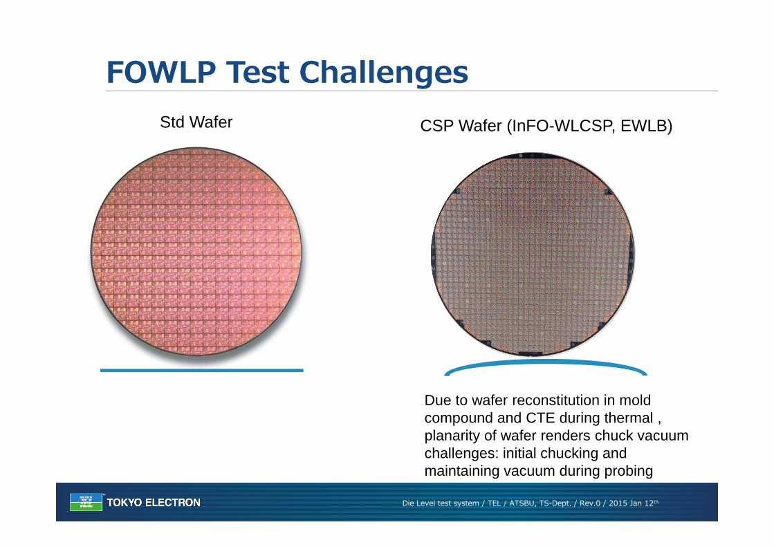
FOWLP Test Challenges Std Wafer CSP Wafer (InFO-WLCSP, EWLB)
Due to wafer reconstitution in mold compound and CTE during thermal , planarity of wafer renders chuck vacuum challenges: initial chucking and maintaining vacuum during probing
Die Level test system / TEL / ATSBU, TS-Dept. / Rev.0 / 2015 Jan 12th
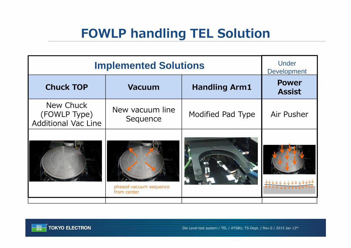
FOWLP handling TEL Solution
Chuck TOP Vacuum Handling Arm1 Power Assist
New Chuck(FOWLP Type)
Additional Vac LineNew vacuum line
Sequence Modified Pad Type Air Pusher
phased vacuum sequence from center
Implemented Solutions Under Development
Wafer Level System Level Test Probing
Die Level test system / TEL / ATSBU, TS-Dept. / Rev.0 / 2015 Jan 12th
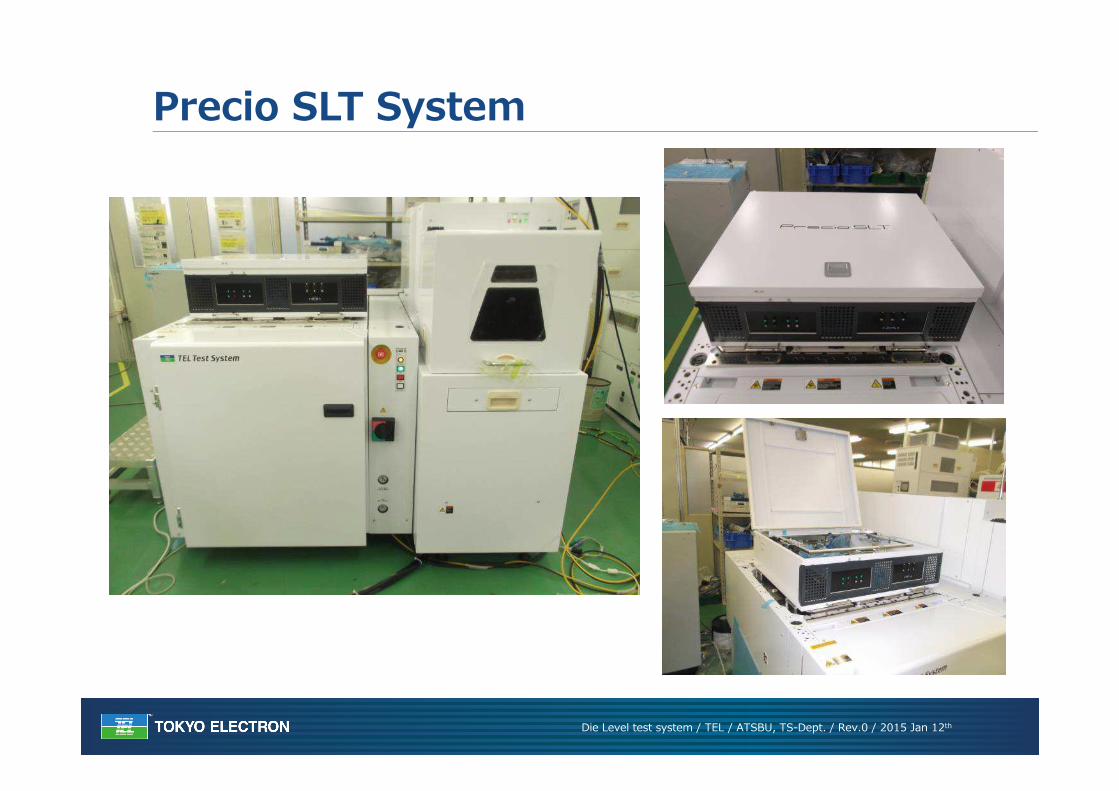
Precio SLT System
Die Level test system / TEL / ATSBU, TS-Dept. / Rev.0 / 2015 Jan 12th
• Packaging continue to Shrink • Testing methods are adapting to the Package
Shrink and Chip Bundling• The Key to the future of Semiconductor Testing is
Package Handling
Summary


