1 a-axis YBa 2 Cu 3 O 7-x /PrBa 2 Cu 3 O 7-x /YBa 2 Cu 3 O 7-x trilayers with subnanometer rms roughness Y. Eren Suyolcu, 1† Jiaxin Sun, 1† Berit H. Goodge, 2 Jisung Park, 1 Jürgen Schubert, 3 Lena F. Kourkoutis, 2,4 and Darrell G. Schlom 1,4,5 1 Department of Materials Sciences and Engineering, Cornell University, Ithaca, New York 14853, USA 2 School of Applied and Engineering Physics, Cornell University, Ithaca, New York 14853, USA 3 Peter Grünberg Institute (PGI-9) and JARA-Fundamentals of Future Information Technology, Forschungszentrum Jülich GmbH, 52425 Jülich, Germany 4 Kavli Institute at Cornell for Nanoscale Science, Ithaca, New York 14853, USA 5 Leibniz-Institut für Kristallzüchtung, Max-Born-Str. 2, 12489 Berlin, Germany † These authors contributed equally to this work
Transcript
1
a-axis YBa2Cu3O7-x/PrBa2Cu3O7-x/YBa2Cu3O7-x
trilayers with subnanometer rms roughness
Y. Eren Suyolcu,1† Jiaxin Sun,1† Berit H. Goodge,2 Jisung Park,1 Jürgen Schubert,3 Lena F.
Kourkoutis,2,4 and Darrell G. Schlom1,4,5
1Department of Materials Sciences and Engineering, Cornell University, Ithaca, New York 14853,
USA
2School of Applied and Engineering Physics, Cornell University, Ithaca, New York 14853, USA
3Peter Grünberg Institute (PGI-9) and JARA-Fundamentals of Future Information Technology,
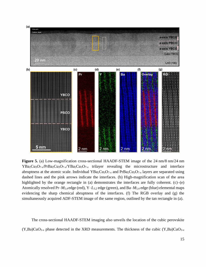
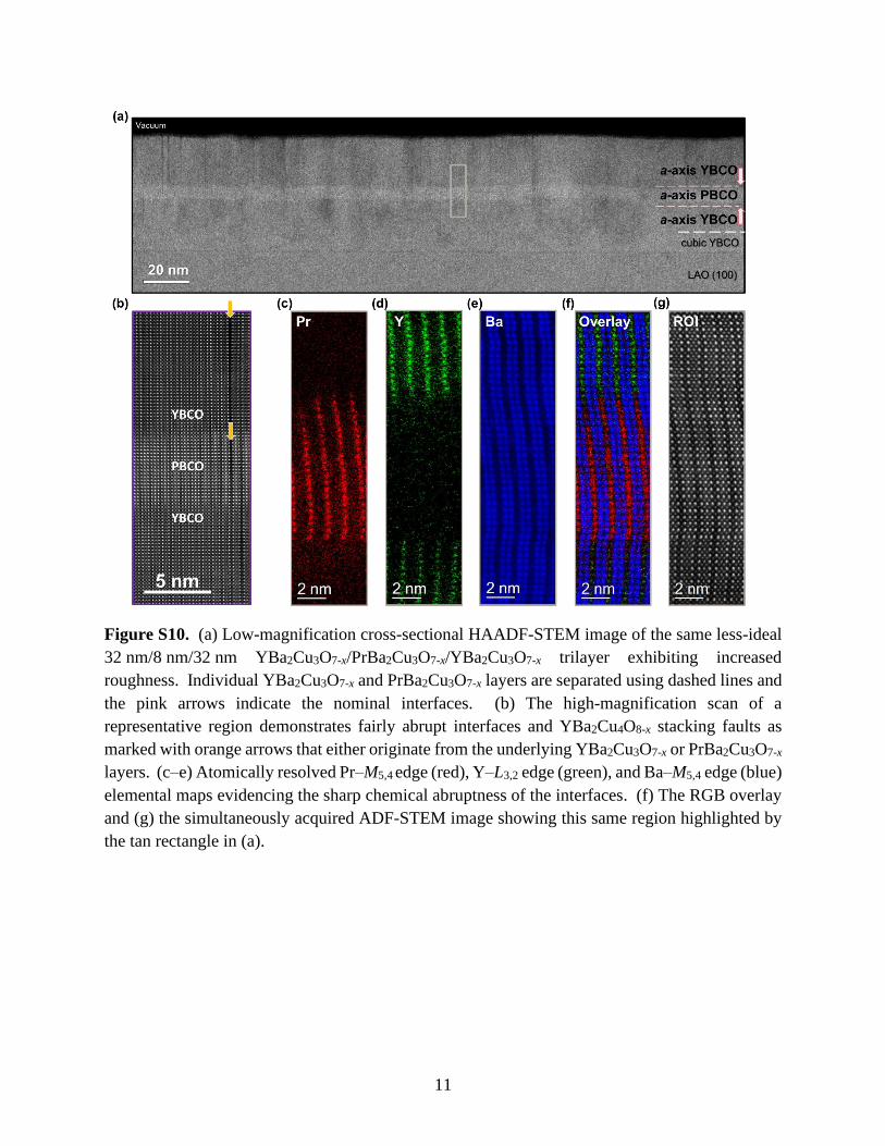
evidencing the sharp chemical abruptness of the interfaces. (f) The RGB overlay and (g) the
simultaneously acquired ADF-STEM image of the same region, outlined by the tan rectangle in (a).
The cross-sectional HAADF-STEM imaging also unveils the location of the cubic perovskite
(Y,Ba)CuO3-x phase detected in the XRD measurements. The thickness of the cubic (Y,Ba)CuO3-x
16
layer is found to be ~10 nm and it is located under the bottom YBa2Cu3O7-x layer (Fig. S7(a)). This
cubic (Y,Ba)CuO3-x layer forms at the start of growth when the substrate is coldest and surface
diffusion is most constrained. Yttrium and barium are unable to diffuse sufficiently far to establish
the Y-Ba-Ba-… ordered arrangement found in the unit cell of YBa2Cu3O7-x; instead yttrium and
barium share the A-site of the resulting perovskite structure, with copper on the B-site.47
As the temperature of the substrate is ramped, the diffusion lengths increase, and in-plane
structural order emerges. The resulting a-axis YBa2Cu3O7-x grains grow epitaxially in one of two
symmetry equivalent orientations: with the c-axis parallel to either [010] or [001] of the cubic
(Y,Ba)CuO3-x layer on which they nucleate on the (100) LaAlO3 substrate. One set of such domains
is clearly seen in Fig. S7: the set with the c-axis along the horizontal direction of the image. The other
set, with the c-axis oriented into the plane of the image, are more difficult to establish because their
spacing along the horizontal direction is the same perovskite spacing as the cubic (Y,Ba)CuO3-x layer
on which they nucleated.
Our hypothesis is that the ~10 nm thick cubic (Y,Ba)CuO3-x layer only lies under the a-axis
oriented YBa2Cu3O7-x layer and that the regions in which this perovskite structure appears to extend
further, i.e., through and all the way to the surface of the trilayer, are actually the set of a-axis domains
oriented with the c-axis running into the plane of the image. This hypothesis is consistent with the
grain size of the a-domains seen in the AFM images (Figs. 3(a)-3(d)) as well as published by others
for a-axis YBa2Cu3O7-x grown on (100) LaAlO3.17,20,33,34,47,48 We know from the XRD -scans (Figs.
2(b) and S5) that there is an equal volume fraction of both 90° in-plane rotation twin variants and
although the volume sampled in our STEM investigation is small, this hypothesis is also consistent
with our STEM observations. Once the substrate temperature is sufficiently high that the a-axis
17
YBa2Cu3O7-x grains nucleate, both twin variants continue through the entire
YBa2Cu3O7-x/PrBa2Cu3O7-x/YBa2Cu3O7-x trilayer.
Lastly, in order to gain insights on the effect of c-axis grains in the trilayers, we perform
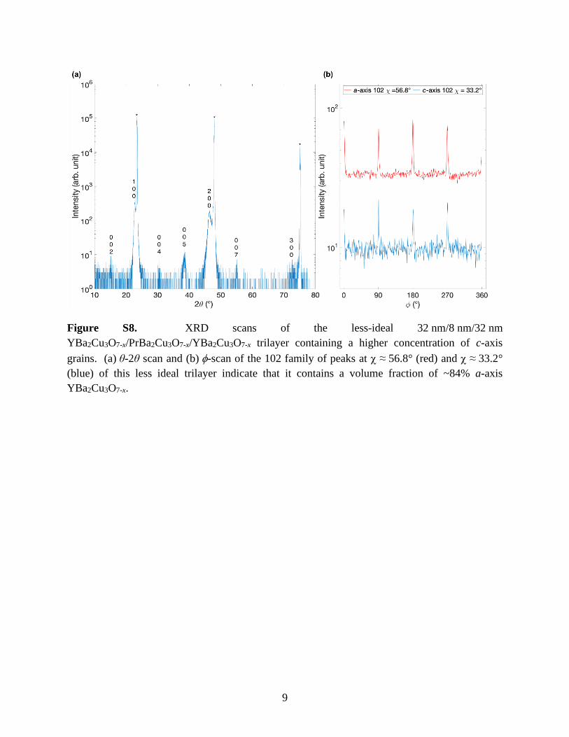
additional cross-sectional STEM investigations on a less-ideal 32 nm/8 nm/32 nm sample. XRD
shows the sample chosen to contain a higher volume fraction (16%) of c-axis oriented
YBa2Cu3O7-x/PrBa2Cu3O7-x (Fig. S8) and to have a higher rms roughness than the 32 nm/8 nm/32 nm
trilayer characterized in Figs. 2-4. HAADF-STEM imaging (Fig. S9) of this less-ideal
32 nm/8 nm/32 nm trilayer confirms the presence of c-axis oriented grains in the structure and also
demonstrates the rougher interfaces. Although the interfaces are rougher, STEM-EELS (Fig. S10)
shows that they remain chemically abrupt. These results, when evaluated together, explain the
rougher surfaces of the thicker samples. The c-axis grain formation in the bottom YBa2Cu3O7-x layer
not only disturbs the PrBa2Cu3O7-x layer (and interface) profiles, but also directly influences the top
surface roughness with changes in the local structural homogeneity in the first layers of the growth.
The strong correlation between surface roughness and the volume fraction of c-axis grains in a-axis
YBa2Cu3O7-x films has been previously noted.39 To avoid c-axis oriented YBa2Cu3O7-x, we initiate
growth at a substrate temperature where only cubic (Y,Ba)CuO3-x can nucleate.
In conclusion, we revisited the growth of a-axis YBa2Cu3O7-x/PrBa2Cu3O7-x/YBa2Cu3O7-x
trilayers and were able to improve their structural quality. By leveraging a temperature-ramping
procedure that begins with a cubic (Y,Ba)CuO3-x buffer layer, we have grown high-quality a-axis
trilayers as confirmed by ex-situ XRD measurements. AFM investigations revealed the improved
surface quality with rms roughness that is less than ξa for the thinnest
YBa2Cu3O7-x/PrBa2Cu3O7-x/YBa2Cu3O7-x trilayers. STEM analyses unveil the interrelation between
18
c-axis oriented regions and surface roughness. Resistivity vs. temperature measurements exhibit an
onset of the superconducting transition at Tonset ~ 85 K and also the widening of the superconducting
transition width with decreasing YBa2Cu3O7-x film thickness. Sharp and coherent interfaces with
limited elemental intermixing are evidenced by atomic-resolution HAADF-STEM and STEM-EELS.
Our findings suggest that with precise control of the growth conditions, the sharp interfaces and
smooth surfaces required in a-axis-based YBa2Cu3O7-x heterostructures for high-performance
Josephson junctions and other oxide electronics are within reach.
19
ACKNOWLEDGMENTS
This work was primarily supported by Ambature, Inc. B.H.G. and L.F.K. acknowledge support
by the Department of Defense Air Force Office of Scientific Research (No. FA 9550-16-1-0305). The
authors thank Ronald Kelly, Michael Lebby, Davis Hartman, Mitch Robson, and Ivan Bozovic for
fruitful discussions. This work made use of a Helios FIB supported by NSF (DMR-1539918) and the
Cornell Center for Materials Research (CCMR) Shared Facilities, which are supported through the
NSF MRSEC Program (Grant No. DMR-1719875). The authors acknowledge Malcolm Thomas,
Donald Werder, John Grazul, and Mariena Silvestry Ramos for assistance in the Electron Microscopy
CCMR facilities. The FEI Titan Themis 300 was acquired through Grant No. NSF-MRI-1429155,
with additional support from Cornell University, the Weill Institute, and the Kavli Institute at Cornell.
This work also made use of the CESI Shared Facilities partly sponsored by the NSF (Grant No. DMR-
1338010) and the Kavli Institute at Cornell. Substrate preparation was performed in part at the Cornell
NanoScale Facility, a member of the National Nanotechnology Coordinated Infrastructure (NNCI),
which is supported by the NSF (Grant No. NNCI-2025233). The authors thank Sean C. Palmer for
his assistance with substrate preparation.
Data availability Statement
The data that support the findings of this study are available from the corresponding author upon
reasonable request.
20
REFERENCES
1 M.K. Wu, J.R. Ashburn, C.J. Torng, P.H. Hor, R.L. Meng, L. Gao, Z.J. Huang, Y.Q. Wang, and
C.W. Chu, Phys. Rev. Lett. 58, 908 (1987). 2 R.J. Cava, B. Batlogg, R.B. van Dover, D.W. Murphy, S. Sunshine, T. Siegrist, J.P. Remeika, E.A.
Rietman, S. Zahurak, and G.P. Espinosa, Phys. Rev. Lett. 58, 1676 (1987). 3 H.-C. Ri, R. Gross, F. Gollnik, A. Beck, R.P. Huebener, P. Wagner, and H. Adrian, Phys. Rev. B
50, 3312 (1994). 4 R.I. Rey, C. Carballeira, J.M. Doval, J. Mosqueira, M.V. Ramallo, A. Ramos-Álvarez, D. Sóñora,
J.A. Veira, J.C. Verde, and F. Vidal, Supercond. Sci. Technol. 32, 045009 (2019). 5 B. Oh, K. Char, A.D. Kent, M. Naito, M.R. Beasley, T.H. Geballe, R.H. Hammond, A. Kapitulnik,
and J.M. Graybeal, Phys. Rev. B 37, 7861 (1988). 6 J.B. Barner, C.T. Rogers, A. Inam, R. Ramesh, and S. Bersey, Appl. Phys. Lett. 59, 742 (1991). 7 R. Gross, L. Alff, A. Beck, O.M. Froehlich, D. Koelle, and A. Marx, IEEE Trans. Appl. Supercond.
7, 2929 (1997). 8 R.H. Koch, C.P. Umbach, G.J. Clark, P. Chaudhari, and R.B. Laibowitz, Appl. Phys. Lett. 51, 200
(1987). 9 J.E. Zimmerman, J.A. Beall, M.W. Cromar, and R.H. Ono, Appl. Phys. Lett. 51, 617 (1987). 10 J. Mannhart, P. Chaudhari, D. Dimos, C.C. Tsuei, and T.R. McGuire, Phys. Rev. Lett. 61, 2476
(1988). 11 D. Koelle, R. Kleiner, F. Ludwig, E. Dantsker, and J. Clarke, Rev. Mod. Phys. 71, 631 (1999). 12 H. Hilgenkamp and J. Mannhart, Rev. Mod. Phys. 74, 485 (2002). 13 S.A. Cybart, E.Y. Cho, T.J. Wong, B.H. Wehlin, M.K. Ma, C. Huynh, and R.C. Dynes, Nature
Nanotechnology 10, 598 (2015). 14 J. Gao, Yu. Boguslavskij, B.B.G. Klopman, D. Terpstra, G.J. Gerritsma, and H. Rogalla, Appl.
Phys. Lett. 59, 2754 (1991). 15 J. Gao, Yu.M. Boguslavskij, B.B.G. Klopman, D. Terpstra, R. Wijbrans, G.J. Gerritsma, and H.
Rogalla, Journal of Applied Physics 72, 575 (1992). 16 H. Asano, M. Asahi, and O. Michikami, Jpn. J. Appl. Phys. 28, L981 (1989). 17 C.B. Eom, A.F. Marshall, S.S. Laderman, R.D. Jacowitz, and T.H. Geballe, Science 249, 1549
(1990). 18 I. Takeuchi, P.A. Warburton, Z. Trajanovic, C.J. Lobb, Z.W. Dong, T. Venkatesan, M.A. Bari,
W.E. Booij, E.J. Tarte, and M.G. Blamire, Appl. Phys. Lett. 69, 112 (1996). 19 F. Miletto Granozio and U.S. di Uccio, Journal of Crystal Growth 174, 409 (1997). 20 A. Inam, C.T. Rogers, R. Ramesh, K. Remschnig, L. Farrow, D. Hart, T. Venkatesan, and B.
Wilkens, Appl. Phys. Lett. 57, 2484 (1990). 21 Z. Trajanovic, I. Takeuchi, P.A. Warburton, C.J. Lobb, and T. Venkatesan, Appl. Phys. Lett. 66,
1536 (1995). 22 A. Inam, R. Ramesh, and C.T. Rogers, 5324714 (28 June 1994). 23 A. Inam, R. Ramesh, and C.T. Rogers, 5358927 (25 October 1994). 24 I. Bozovic, J.N. Eckstein, N. Bozovic, and J. O’Donnell, MRS Online Proceedings Library Archive
502, (1997). 25 R. Baghdadi, R. Arpaia, E. Stepantsov, M. Arzeo, D. Golubev, D. Montemurro, E. Andersson, T.
Bauch, and F. Lombardi, Phys. Rev. B 95, 184505 (2017).
21
26 G.W. Berkstresser, A.J. Valentino, and C.D. Brandle, Journal of Crystal Growth 128, 684 (1993). 27 P.D.C. King, H.I. Wei, Y.F. Nie, M. Uchida, C. Adamo, S. Zhu, X. He, I. Božović, D.G. Schlom,
and K.M. Shen, Nature Nanotechnology 9, 443 (2014). 28 M. Park, M.J. Kramer, K.W. Dennis, and R.W. McCallum, Physica C: Superconductivity and Its
Applications 259, 43 (1996). 29 J.A. Edwards, N.G. Chew, S.W. Goodyear, J.S. Satchell, S.E. Blenkinsop, and R.G. Humphreys,
Journal of the Less Common Metals 164–165, 414 (1990). 30 J.A. Agostinelli, S. Chen, and G. Braunstein, Phys. Rev. B 43, 11396 (1991). 31 M. Bosman, M. Watanabe, D.T.L. Alexander, and V.J. Keast, Ultramicroscopy 106, 1024 (2006). 32 C. Giacovazzo, H.L. Monaco, G. Artioli, D. Viterbo, G. Ferraris, G. Gilli, G. Zanotti, and M. Catti,
Fundamentals of Crystallography, 2nd Edition (Oxford University Press, Oxford ; New York, 2002). 33 R. Ramesh, A. Inam, D.M. Hwang, T.S. Ravi, T. Sands, X.X. Xi, X.D. Wu, Q. Li, T. Venkatesan,
and R. Kilaas, Journal of Materials Research 6, 2264 (1991). 34 A.F. Marshall and C.B. Eom, Physica C: Superconductivity 207, 239 (1993). 35 H.M. Appelboom, V.C. Matijasevic, F. Mathu, G. Rietveld, B. Anczykowski, W.J.A.M. Peterse,
F. Tuinstra, J.E. Mooij, W.G. Sloof, H.A. Rijken, S.S. Klein, and L.J. van IJzendoorn, Physica C:
Superconductivity 214, 323 (1993). 36 J.A. Agostinelli, S. Chen, and G. Braunstein, Physica C: Superconductivity 180, 26 (1991). 37 S. Chan, D.M. Hwang, and L. Nazar, Journal of Applied Physics 65, 4719 (1989). 38 P. Berberich, B. Utz, W. Prusseit, and H. Kinder, Physica C: Superconductivity 219, 497 (1994). 39 T. Umezawa, D.J. Lew, S.K. Streiffer, and M.R. Beasley, Appl. Phys. Lett. 63, 3221 (1993). 40 D. Putzky, P. Radhakrishnan, Y. Wang, P. Wochner, G. Christiani, M. Minola, P.A. van Aken, G.
Logvenov, E. Benckiser, and B. Keimer, Appl. Phys. Lett. 117, 072601 (2020). 41 S.J. Pennycook, Ultramicroscopy 30, 58 (1989). 42 Y.E. Suyolcu, Y. Wang, F. Baiutti, A. Al-Temimy, G. Gregori, G. Cristiani, W. Sigle, J. Maier,
P.A. van Aken, and G. Logvenov, Scientific Reports 7, 453 (2017). 43 Y.E. Suyolcu, G. Christiani, P.A. van Aken, and G. Logvenov, J Supercond Nov Magn 33, 107
(2020). 44 H.W. Zandbergen, R. Gronsky, K. Wang, and G. Thomas, Nature 331, 596 (1988). 45 R. Ramesh, D.M. Hwang, J.B. Barner, L. Nazar, T.S. Ravi, A. Inam, B. Dutta, X.D. Wu, and T.
Venkatesan, Journal of Materials Research 5, 704 (1990). 46 H. Zhang, N. Gauquelin, G.A. Botton, and J.Y.T. Wei, Appl. Phys. Lett. 103, 052606 (2013). 47 S.K. Streiffer, B.M. Lairson, E.M. Zielinski, and J.C. Bravman, Phys. Rev. B 47, 11431 (1993). 48 S.K. Streiffer, B.M. Lairson, E.M. Zielinski, and J.C. Bravman, MRS Online Proceedings Library
Archive 275, (1992).
1
Supplementary Material
a-axis YBa2Cu3O7-x/PrBa2Cu3O7-x/YBa2Cu3O7-x
trilayers with subnanometer rms roughness
Y. Eren Suyolcu1†, Jiaxin Sun1†, Berit H. Goodge2, Jisung Park1, Jürgen Schubert3, Lena F.
Kourkoutis2,4, and Darrell G. Schlom1,4,5
1Department of Materials Sciences and Engineering, Cornell University, Ithaca, New York 14853,
USA
2School of Applied and Engineering Physics, Cornell University, Ithaca, New York 14853, USA
3Peter Grünberg Institute (PGI-9) and JARA-Fundamentals of Future Information Technology,
elemental maps evidencing the sharp chemical abruptness of the interfaces. (f) The RGB overlay
and (g) the simultaneously acquired ADF-STEM image showing this same region highlighted by
the tan rectangle in (a).
12
References
1 T. Terashima, Y. Bando, K. Iijima, K. Yamamoto, K. Hirata, K. Hayashi, K. Kamigaki, and H.
Terauchi, Phys. Rev. Lett. 65, 2684 (1990). 2 C. Korte, A. Peters, J. Janek, D. Hesse, and N. Zakharov, Phys. Chem. Chem. Phys. 10, 4623
(2008). 3 D.C. Sayle and G.W. Watson, J. Phys. Chem. B 105, 5506 (2001). 4 K. Kawaguchi, R. Kita, M. Nishiyama, and T. Morishita, Journal of Crystal Growth 143, 221