TRIPLE OUTPUT LCD SUPPLY WITH LINEAR REGULATOR AND POWER GOOD
• 2.7-V to 5.8-V Input Voltage Range The TPS65140/145 offers a compact and smallpower supply solution to provide all three voltages• 1.6-MHz Fixed Switching Frequencyrequired by thin film transistor (TFT) LCD displays.• 3 Independent Adjustable OutputsThe auxiliary linear regulator controller can be used
• Main Output up to 15 V With <1% Typical to generate a 3.3-V logic power rail for systemsOutput Voltage Accuracy powered by a 5-V supply rail only.
• Negative Output Voltage Down to -12 V/20 mA The main output Vo1 is a 1.6-MHz fixed frequency• Positive Output Voltage up to 30 V/20 mA PWM boost converter providing the source drive
voltage for the LCD display. The device is available in• Auxiliary 3.3-V Linear Regulator Controllertwo versions with different internal switch current• Internal Soft Startlimits to allow the use of a smaller external inductor
• Internal Power-On Sequencing when lower output power is required. The TPS65140has a typical switch current limit of 2.3 A and the• Fault Detection of all OutputsTPS65145 has a typical switch current limit of 1.37 A.• Thermal ShutdownA fully integrated adjustable charge pump
• System Power Good doubler/tripler provides the positive LCD gate drivevoltage. An externally adjustable negative charge• Available in TSSOP-24 and QFN-24pump provides the negative gate drive voltage. DuePowerPAD™ Packagesto the high 1.6-MHz switching frequency of thecharge pumps, inexpensive and small 220-nF capaci-tors can be used.• TFT LCD Displays for NotebooksAdditionally, the TPS65140/145 has a system power• TFT LCD Displays for Monitorsgood output to indicate when all supply rails are• Portable DVD Playersacceptable. For LCD panels powered by 5 V, only the
• Tablet PCs TPS65140/145 has a linear regulator controller using• Car Navigation Systems an external transistor to provide a regulated 3.3 V
output for the digital circuits. For maximum safety, the• Industrial Displaysentire device goes into shutdown as soon as one ofthe outputs is out of regulation. The device can beenabled again by toggling the input or the enable(EN) pin to GND.
Please be aware that an important notice concerning availability, standard warranty, and use in critical applications of TexasInstruments semiconductor products and disclaimers thereto appears at the end of this data sheet.
TPS65140TPS65145SLVS497B–SEPTEMBER 2003–REVISED MARCH 2004
These devices have limited built-in ESD protection. The leads should be shorted together or the device placed in conductive foamduring storage or handling to prevent electrostatic damage to the MOS gates.
TYPICAL APPLICATION CIRCUIT
ORDERING INFORMATION
PACKAGE (1)
LINEAR REGULATOR MINIMUM SWITCHTA PACKAGEOUTPUT VOLTAGE CURRENT LIMIT TSSOP QFN MARKING
3.3 V 1.6 A TPS65140PWP TPS65140RGE TPS65140-40°C to 85°C
3.3 V 0.96 A TPS65145PWP TPS65145RGE TPS65145
(1) The PWP and RGE packages are available taped and reeled. Add an R suffix to the device type (TPS65100PWPR) to order the devicetaped and reeled. The PWPR package has quantities of 2000 devices per reel, and the the RGER package has 3000 devices per reel.Without the suffix, the PWP package only, is shipped in tubes with 60 devices per tube.
2
www.ti.com
ABSOLUTE MAXIMUM RATINGS
DISSIPATION RATINGS
RECOMMENDED OPERATING CONDITIONS
ELECTRICAL CHARACTERISTICS
TPS65140TPS65145
SLVS497B–SEPTEMBER 2003–REVISED MARCH 2004
over operating free-air temperature range (unless otherwise noted) (1)
UNIT
Voltages on pin VIN (2) -0.3 V to 6.0 V
Voltages on pin Vo1, SUP, PG (2) -0.3 V to 15.5 V
Voltages on pin EN, MODE, ENR (2) -0.3 V to VI + 0.3 V
Voltage on pin SW (2) 20 V
Power good maximum sink current (PG) 1 mA
Continuous power dissipation See Dissipation Rating Table
Operating junction temperature range -40°C to 150°C
Storage temperature range -65°C to 150°C
Lead temperature (soldering, 10 sec) 260°C
(1) Stresses beyond those listed under “absolute maximum ratings” may cause permanent damage to the device. These are stress ratingsonly, and functional operation of the device at these or any other conditions beyond those indicated under “recommended operatingconditions” is not implied. Exposure to absolute-maximum-rated conditions for extended periods may affect device reliability.
(2) All voltage values are with respect to network ground terminal.
TA≤ 25°C TA = 70°C TA = 85°CPACKAGE RΘJA POWER RATING POWER RATING POWER RATING
24-Pin TSSOP 30.13 C°/W (PWP soldered) 3.3 W 1.83 W 1.32 W
24-Pin QFN 30.0 C°/W 3.3 W 1.8 W 1.3 W
MIN TYP MAX UNIT
VIN Input voltage range 2.7 5.8 V
L Inductor (1) 4.7 µH
TA Operating ambient temperature -40 85 °C
TJ Operating junction temperature -40 125 °C
(1) Refer to the application information section for further information.
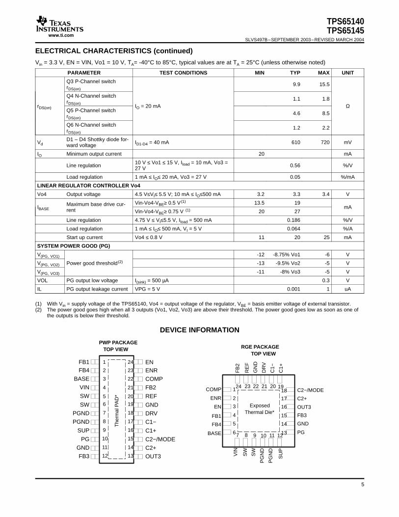
Vin = 3.3 V, EN = VIN, Vo1 = 10 V, TA= -40°C to 85°C, typical values are at TA = 25°C (unless otherwise noted)
PARAMETER TEST CONDITIONS MIN TYP MAX UNIT
SUPPLY CURRENT
Vin Input voltage range 2.7 5.5 V
ENR = GND, Vo3 = 2 × Vo1, 0.7 0.9 mAIQIN Quiescent current into VIN Boost converter not switching
D1 – D4 Shottky diode for-Vd ID1-D4 = 40 mA 610 720 mVward voltage
IO Minimum output current 20 mA
10 V ≤ Vo1 ≤ 15 V, Iload = 10 mA, Vo3 =Line regulation 0.56 %/V27 V
Load regulation 1 mA ≤ IO≤ 20 mA, Vo3 = 27 V 0.05 %/mA
LINEAR REGULATOR CONTROLLER Vo4
Vo4 Output voltage 4.5 V≤VI≤ 5.5 V; 10 mA ≤ IO≤500 mA 3.2 3.3 3.4 V
Vin-Vo4-VBE≥ 0.5 V (1) 13.5 19Maximum base drive cur-IBASE mArent Vin-Vo4-VBE≥ 0.75 V (1) 20 27
Line regulation 4.75 V ≤ VI≤5.5 V, Iload = 500 mA 0.186 %/V
Load regulation 1 mA ≤ IO≤ 500 mA, VI = 5 V 0.064 %/A
Start up current Vo4 ≤ 0.8 V 11 20 25 mA
SYSTEM POWER GOOD (PG)
V(PG, VO1) -12 -8.75% Vo1 -6 V
V(PG, VO2) Power good threshold (2) -13 -9.5% Vo2 -5 V
V(PG, VO3) -11 -8% Vo3 -5 V
VOL PG output low voltage I(sink) = 500 µA 0.3 V
IL PG output leakage current VPG = 5 V 0.001 1 uA
(1) With Vin = supply voltage of the TPS65140, Vo4 = output voltage of the regulator, VBE = basis emitter voltage of external transistor.(2) The power good goes high when all 3 outputs (Vo1, Vo2, Vo3) are above their threshold. The power good goes low as soon as one of
the outputs is below their threshold.
5
www.ti.com
TPS65140TPS65145SLVS497B–SEPTEMBER 2003–REVISED MARCH 2004
DEVICE INFORMATION (continued)Terminal Functions
TERMINALI/O DESCRIPTIONNO.NAME NO. (RGE)(PWP)
VIN 4 7 I Input voltage pin of the device.
Enable pin of the device. This pin should be terminated and not be left floating. A logicEN 24 3 I high enables the device and a logic low shuts down the device.
COMP 22 1 Compensation pin for the main boost converter. A small capacitor is connected to thispin.
Open drain output indicating when all outputs Vo1, Vo2, Vo3 are within 10% of theirPG 10 13 O nominal output voltage. The output goes low when one of the outputs falls below 10%
of their nominal output voltage.
Enable pin of the linear regulator controller. This pin should be terminated and not beENR 23 2 I left floating. Logic high enables the regulator and a logic low puts the regulator in
shutdown.
C1+ 16 19 Positive terminal of the charge pump flying capacitor
C1- 17 20 Negative terminal of the charge pump flying capacitor
DRV 18 21 O External charge pump driver
FB2 21 24 I Feedback pin of negative charge pump
REF 20 23 O Internal reference output typically 1.23 V
Feedback pin of the linear regulator controller. The linear regulator controller is set to aFB4 2 5 I fixed output voltage of 3.3 V or 3.0 V depending on the version.
BASE 3 6 O Base drive output for the external transistor
GND 11, 19 14, 22 Ground
PGND 7, 8 10, 11 Power ground
FB3 12 15 I Feedback pin of positive charge pump
OUT3 13 16 O Positive charge pump output
Negative terminal of the charge pump flying capacitor and charge pump MODE pin. Ifthe flying capacitor is connected to this pin, the converter operates in a voltage triplerC2-/MODE 15 18 mode. If the charge pump needs to operate in a voltage doubler mode, the flyingcapacitor is removed and the C2-/MODE pin needs to be connected to GND.
Positive terminal for the charge pump flying capacitor. If the device runs in voltageC2+ 14 17 doubler mode, this pin needs to be left open.
Supply pin of the positive, negative charge pump, boost converter, and gate drivecircuit. This pin needs to be connected to the output of the main boost converter andSUP 9 12 I cannot be connected to any other voltage source. For performance reasons, it is notrecommended for a bypass capacitor to be connected directly to this pin.
FB1 1 4 I Feedback pin of the boost converter
SW 5, 6 8, 9 I Switch pin of the boost converter
PowerPAD The PowerPAD or exposed thermal die needs to be connected to power ground pins™/Thermal (PGND)Die
POWER-UP SEQUENCING SOFT START Vo1 Vo2 MAXIMUM LOAD CURRENT
Figure 10. Figure 11. Figure 12.
9
www.ti.com
0
0.02
0.04
0.06
0.08
0.10
0.12
0.14
9 10 11 12 13 14 15
Vo1 − Output Voltage − V
− O
utp
ut
Cu
rren
t −
AI O
Vo3 = 18 V (Doubler Mode)
TA = 25°C
TA = 85°CTA = −40°C
0
0.02
0.04
0.06
0.08
0.10
0.12
9 10 11 12 13 14 15
Vo1 − Output Voltage − V
− O
utp
ut
Cu
rren
t −
AI O
Vo3 = 28 V (Tripler Mode)
TA = 25°C
TA = 85°C
TA = −40°C
DETAILED DESCRIPTION
Main Boost Converter
Power-Good Output
Enable and Power-On Sequencing (EN, ENR)
TPS65140TPS65145SLVS497B–SEPTEMBER 2003–REVISED MARCH 2004
TYPICAL CHARACTERISTICS (continued)
Vo3 MAXIMUM LOAD CURRENT Vo3 MAXIMUM LOAD CURRENT
Figure 13. Figure 14.
The TPS65140/45 consists of a main boost converter operating with a fixed switching frequency of 1.6 MHz toallow for small external components. The boost converter output voltage Vo1 is also the input voltage, connectedvia the pin SUP, for the positive and negative charge pump. The linear regulator controller is independent fromthis system with its own enable pin. This allows the linear regulator controller to continue to operate while theother supply rails are disabled or in shutdown due to a fault condition on one of their outputs. Refer to thefunctional block diagram for more information.
The main boost converter operates with PWM and a fixed switching frequency of 1.6 MHz. The converter uses aunique fast response, voltage mode controller scheme with input voltage feedforward. This achieves excellentline and load regulation (0.2% A load regulation typical) and allows the use of small external components. To addhigher flexibility to the selection of external component values, the device uses external loop compensation.Although the boost converter looks like a nonsynchronous boost converter topology operating in discontinuousmode at light load, the TPS65140/45 maintains continuous conduction even at light load currents.
This is achieved with a novel architecture using an external Schottky diode and an integrated MOSFET in parallelconnected between SW and SUP (see the functional block diagram). The integrated MOSFET Q2 allows theinductor current to become negative at light load conditions. For this purpose, a small integrated P-channelMOSFET with typically 10 Ω rDS(on) is sufficient. When the inductor current is positive, the external Schottky diodewith the lower forward voltage conducts the current. This causes the converter to operate with a fixed frequencyin continuous conduction mode over the entire load current range. This avoids the ringing on the switch pin asseen with a standard nonsynchronous boost converter and allows a simpler compensation for the boostconverter.
The TPS65140/45 has an open-drain power-good output with a maximum sink capability of 1 mA. Thepower-good output goes high as soon as the main boost converter Vo1 and the negative and the positive chargepumps are within regulation. The power-good output goes low as soon as one of the outputs is out of regulation.In this case, the device goes into shutdown at the same time. See the electrical characteristics table for thepower-good thresholds.
The device has two enable pins. These pins should be terminated and not left floating to prevent faulty operation.Pulling the enable pin (EN) high enables the device and starts the power-on sequencing with the main boostconverter Vo1 coming up first, then the negative and positive charge pumps. The linear regulator has anindependent enable pin (ENR). Pulling this pin low disables the regulator, and pulling this pin high enables thisregulator.
10
www.ti.com
Positive Charge Pump
Negative Charge Pump
Linear Regulator Controller
Soft Start
Fault Protection
Thermal Shutdown
TPS65140TPS65145
SLVS497B–SEPTEMBER 2003–REVISED MARCH 2004
If the enable pin (EN) is pulled high, the device starts its power-on sequencing. The main boost converter startsup first with its soft start. If the output voltage has reached 91.25% of its output voltage, the negative chargepump comes up next. The negative charge pump starts with a soft start and when the output voltage hasreached 91% of the nominal value, the positive charge pump comes up with the soft start.
Pulling the enable pin low shuts down the device. Dependent on load current and output capacitance, each ofthe outputs comes down.
The TPS65140/45 has a fully regulated integrated positive charge pump generating Vo3. The input voltage forthe charge pump is applied to the SUP pin that is equal to the output of the main boost converter Vo1. Thecharge pump is capable of supplying a minimum load current of 20 mA. Higher load currents are possibledepending on the voltage difference between Vo1 and Vo3. See Figure 13 and Figure 14.
The TPS65140/45 has a regulated negative charge pump using two external Schottky diodes. The input voltagefor the charge pump is applied to the SUP pin that is connected to the output of the main boost converter Vo1.The charge pump inverts the main boost converter output voltage and is capable of supplying a minimum loadcurrent of 20 mA. Higher load currents are possible depending on the voltage difference between Vo1 and Vo2.See Figure 12.
The TPS65140/45 includes a linear regulator controller to generate a 3.3-V rail which is useful when the systemis powered from a 5-V supply. The regulator is independent from the other voltage rails of the device and has itsown enable (ENR).
The main boost converter as well as the charge pumps and linear regulator have an internal soft start. Thisavoids heavy voltage drops at the input voltage rail or at the output of the main boost converter Vo1 duringstart-up caused by high inrush currents. See Figure 10 and Figure 11.
All of the outputs of the TPS65140/45 have short-circuit detection and cause the device to go into shutdown. Themain boost converter has overvoltage and undervoltage protection. If the output voltage Vo1 rises above theovervoltage protection threshold of typically 5% of Vo1, then the device stops switching, but remains operational.When the output voltage falls below this threshold, the converter continues operation. When the output voltagefalls below the undervoltage protection threshold of typically 8.75% of Vo1, because of a short-circuit condition,the TPS65140/45 goes into shutdown. Because there is a direct pass from the input to the output through thediode, the short-circuit condition remains. If this condition needs to be avoided, a fuse at the input or an outputdisconnect using a single transistor and resistor is required. The negative and positive charge pumps have anundervoltage lockout (UVLO) to protect the LCD panel of possible latch-up conditions due to a short-circuitcondition or faulty operation. When the negative output voltage is typically above 9.5% of its output voltage(closer to ground), then the device enters shutdown. When the positive charge pump output voltage, Vo3, isbelow 8% typical of its output voltage, the device goes into shutdown. See the fault protection thresholds in theelectrical characteristics table. The device is enabled by toggling the enable pin (EN) below 0.4 V or by cyclingthe input voltage below the UVLO of 1.7 V. The linear regulator reduces the output current to 20 mA typicalunder a short-circuit condition when the output voltage is typically < 1 V. See the functional block diagram. Thelinear regulator does not go into shutdown under a short-circuit condition.
A thermal shutdown is implemented to prevent damage due to excessive heat and power dissipation. Typically,the thermal shutdown threshold is 160°C. If this temperature is reached, the device goes into shutdown. Thedevice can be enabled by toggling the enable pin to low and back to high or by cycling the input voltage to GNDand back to VI again.
11
www.ti.com
APPLICATION INFORMATION
BOOST CONVERTER DESIGN PROCEDURE
DVout VD VinVout VD Vsw
10 V 0.8 V 3.3 V10 V 0.8 V 0.5 V
0.73
IL
Iout1 D
300 mA1 0.73
1.11 A
iL Vin Vsw D
fs L
(3.3 V 0.5 V) 0.731.6 MHz 4.2 H
304 mA
Iswpeak IL
iL2
1.11 A 304 mA
2 1.26 A
Inductor Selection
TPS65140TPS65145SLVS497B–SEPTEMBER 2003–REVISED MARCH 2004
The first step in the design procedure is to calculate the maximum possible output current of the main boostconverter under certain input and output voltage conditions. Below is an example for a 3.3-V to 10-V conversion:
Vin = 3.3 V, Vout = 10 V, Switch voltage drop Vsw = 0.5 V, Schottky diode forward voltage VD = 0.8 V1. Duty cycle:
2. Average inductor current:
3. Inductor peak-to-peak ripple current:
4. Peak switch current:
The integrated switch, the inductor, and the external Schottky diode must be able to handle the peak switchcurrent. The calculated peak switch current has to be equal or lower to the minimum N-MOSFET switch currentlimit as specified in the electrical characteristics table (1.6 A for the TPS65140 and 0.96 A for the TPS65145). Ifthe peak switch current is higher, then the converter cannot support the required load current. This calculationmust be done for the minimum input voltage where the peak switch current is highest. The calculation includesconduction losses like switch rDS(on) (0.5 V) and diode forward drop voltage losses (0.8 V). Additional switchinglosses, inductor core and winding losses, etc., require a slightly higher peak switch current in the actualapplication. The above calculation still allows for a good design and component selection.
Several inductors work with the TPS65140. Especially with the external compensation, the performance can beadjusted to the specific application requirements. The main parameter for the inductor selection is the saturationcurrent of the inductor which should be higher than the peak switch current as calculated above with additionalmargin to cover for heavy load transients and extreme start-up conditions. Another method is to choose theinductor with a saturation current at least as high as the minimum switch current limit of 1.6 A for the TPS65140and 0.96 A for the TPS65145. The different switch current limits allow selection of a physically smaller inductorwhen less output current is required. The second important parameter is the inductor dc resistance. Usually, thelower the dc resistance, the higher the efficiency. However, the inductor dc resistance is not the only parameterdetermining the efficiency. Especially for a boost converter where the inductor is the energy storage element, thetype and material of the inductor influences the efficiency as well. Especially at high switching frequencies of 1.6MHz, inductor core losses, proximity effects, and skin effects become more important. Usually, an inductor with alarger form factor yields higher efficiency. The efficiency difference between different inductors can vary between2% to 10%. For the TPS65140, inductor values between 3.3 µH and 6.8 µH are a good choice but other valuescan be used as well. Possible inductors are shown in Table 1.
12
www.ti.com
Output Capacitor Selection
Vout IoutCout
1fs
Ip L
Vout Vd Vin Ip ESR
Ip = Peak current as described in the previous section peak current control L = Selected inductor valueIout = Nominal load currentfs = Switching frequencyVd = Rectifier diode forward voltage (typically 0.3 V)Cout = Selected output capacitorESR = Output capacitor ESR value
Input Capacitor Selection
Rectifier Diode Selection
TPS65140TPS65145
SLVS497B–SEPTEMBER 2003–REVISED MARCH 2004
APPLICATION INFORMATION (continued)Table 1. Inductor Selection
DEVICE INDUCTOR VALUE COMPONENT SUPPLIER DIMENSIONS ISAT/DCR
For best output voltage filtering, a low ESR output capacitor is recommended. Ceramic capacitors have a lowESR value but depending on the application, tantalum capacitors can be used as well. A 22-µF ceramic outputcapacitor works for most of the applications. Higher capacitor values can be used to improve load transientregulation. See Table 2 for the selection of the output capacitor. The output voltage ripple can be calculated as:
with:
For good input voltage filtering, low ESR ceramic capacitors are recommended. A 22-µF ceramic input capacitoris sufficient for most of applications. For better input voltage filtering, this value can be increased. See Table 2and the typical applications for input capacitor recommendations.
Table 2. Input and Output Capacitors Selection
CAPACITOR VOLTAGE RATING COMPONENT SUPPLIER COMMENTS
22 µF/1210 16V Taiyo Yuden EMK325BY226MM CO
22 µF/1206 6.3V Taiyo Yuden JMK316BJ226 CI
To achieve high efficiency, a Schottky diode should be used. The voltage rating should be higher than themaximum output voltage of the converter. The average forward current should be equal to the average inductorcurrent of the converter. The main parameter influencing the efficiency of the converter is the forward voltage andthe reverse leakage current of the diode; both should be as low as possible. Possible diodes are: OnSemiconductor MBRM120L, Microsemi UPS120E, and Fairchild Semiconductor MBRS130L.
13
www.ti.com
Converter Loop Design and Stability
Design Procedure Quick Steps
Setting the Output Voltage and Selecting the Feedforward Capacitor
Vout 1.146 V 1 R1R2
SWSWFB1SUP
C2+C2−/MODE
D1
C86.8 pF
R1430 kΩ
R256 kΩ
C422 µF
VO1Up to 10 V/150 mA
C2 0.22 µF
C8 1
2 fz R1
12 50 kHz R1
TPS65140TPS65145SLVS497B–SEPTEMBER 2003–REVISED MARCH 2004
The TPS65140/45 converter loop can be externally compensated and allows access to the internaltransconductance error amplifier output at the COMP pin. A small feedforward capacitor across the upperfeedback resistor divider speeds up the circuit as well. To test the converter stability and load transientperformance of the converter, a load step from 50 mA to 250 mA is applied and the output voltage of theconverter is monitored. Applying load steps to the converter output is a good tool to judge the stability of such aboost converter.
1. Select the feedback resistor divider to set the output voltage.2. Select the feedforward capacitor to place a zero at 50 kHz.3. Select the compensation capacitor on pin COMP. The smaller the value, the higher the low frequency gain.4. Use a 50-kΩ potentiometer in series to Cc and monitor Vout during load transients. Fine tune the load
transient by adjusting the potentiometer. Select a resistor value that comes closest to the potentiometerresistor value. This needs to be done at the highest Vin and highest load current because stability is mostcritical at these conditions.
The output voltage is set by the external resistor divider and is calculated as:
Across the upper resistor, a bypass capacitor is required to speed up the circuit during load transients as shownin Figure 15.
Figure 15. Feedforward Capacitor
Together with R1 the bypass capacitor C8 sets a zero in the control loop at approximately 50 kHz:
A value closest to the calculated value should be used. Larger feedforward capacitor values reduce the loadregulation of the converter and cause load steps as shown in Figure 16.
14
www.ti.com
Load Step
Compensation
VIN
COMPRC
15 kΩ
CC
1 nF
fz 1
2 Cc Rc
CC = 4.7 nF
TPS65140TPS65145
SLVS497B–SEPTEMBER 2003–REVISED MARCH 2004
Figure 16. Load Step Caused By A Too Large Feedforward Capacitor Value
The regulator loop can be compensated by adjusting the external components connected to the COMP pin. TheCOMP pin is connected to the output of the internal transconductance error amplifier. A typical compensationscheme is shown in Figure 17.
Figure 17. Compensation Network
The compensation capacitor Cc adjusts the low frequency gain, and the resistor value adjusts the high frequencygain. The following formula calculates at what frequency the resistor increases the high frequency gain.
Lower input voltages require a higher gain and a lower compensation capacitor value. A good start is Cc = 1 nFfor a 3.3-V input and Cc = 2.2 nF for a 5-V input. If the device operates over the entire input voltage range from2.7 V to 5.8 V, a larger compensation capacitor up to 10 nF is recommended. Figure 18 shows the load transientwith a larger compensation capacitor, and Figure 19 shows a smaller compensation capacitor.
Figure 18. CC = 4. 7 nF
15
www.ti.com
CC = 1 nF
TPS65140TPS65145SLVS497B–SEPTEMBER 2003–REVISED MARCH 2004
Figure 19. CC = 1 nF
Lastly, Rc needs to be selected. A good practice is to use a 50-kΩ potentiometer and adjust the potentiometer forthe best load transient where no oscillations should occur. These tests have to be done at the highest Vin andhighest load current because the converter stability is most critical under these conditions. Figure 20, Figure 21,and Figure 22 show the fine tuning of the loop with Rc.
Figure 20. Overcompensated (Damped Oscillation), RC Is Too Large
Figure 21. Undercompensated (Loop Is Too Slow), RC Is Too Small
16
www.ti.com
Vout VREF 1 R3R4 VREF 1.213 V 1 R3
R4 1.213 V
R3 R4 Vout
VREFVREF
1 R4 Vout
1.213
1.213 1
TPS65140TPS65145
SLVS497B–SEPTEMBER 2003–REVISED MARCH 2004
Figure 22. Optimum, RC Is Ideal
Negative Charge Pump
The negative charge pump provides a regulated output voltage by inverting the main output voltage, Vo1. Thenegative charge pump output voltage is set with external feedback resistors.
The maximum load current of the negative charge pump depends on the voltage drop across the externalSchottky diodes, the internal on resistance of the charge pump MOSFETS Q8 and Q9, and the impedance of theflying capacitor, C12. When the voltage drop across these components is larger than the voltage difference fromVo1 to Vo2, the charge pump is in drop out, providing the maximum possible output current. Therefore, thehigher the voltage difference between Vo1 and Vo2, the higher the possible load current. See Figure 12 for thepossible output current versus boost converter voltage Vo1 and the calculations below.
The lower feedback resistor value, R4, should be in a range between 40 kΩ to 120 kΩ or the overall feedbackresistance should be within 500 kΩ to 1 MΩ. Smaller values load the reference too heavy and larger values maycause stability problems. The negative charge pump requires two external Schottky diodes. The peak currentrating of the Schottky diode has to be twice the load current of the output. For a 20 mA output current, the dualSchottky diode BAT54 or similar is a good choice.
Positive Charge Pump
The positive charge pump can be operated in a voltage doubler mode or a voltage tripler mode depending on theconfiguration of the C2+ and C2-/MODE pins. Leaving the C2+ pin open and connecting C2-/MODE to GNDforces the positive charge pump to operate in a voltage doubler mode. If higher output voltages are required thepositive charge pump can be operated as a voltage tripler. To operate the charge pump in the voltage triplermode, a flying capacitor needs to be connected to C2+ and C2-/MODE.
The maximum load current of the positive charge pump depends on the voltage drop across the internal Schottkydiodes, the internal on-resistance of the charge pump MOSFETS, and the impedance of the flying capacitor.When the voltage drop across these components is larger than the voltage difference Vo1 × 2 to Vo3 (doublermode) or Vo1 × 3 to Vo3 (tripler mode), then the charge pump is in dropout, providing the maximum possibleoutput current. Therefore, the higher the voltage difference between Vo1 × 2 (doubler) or Vo1 × 3 (tripler) to Vo3,the higher the possible load current. See Figure 13 and Figure 14 for output current versus boost convertervoltage, Vo1, and the following calculations.
The output voltage is set by the external resistor divider and is calculated as:
Linear Regulator Controller
The TPS65100/05 includes a linear regulator controller to generate a 3.3-V rail when the system is powered froma 5-V supply. Because an external npn transistor is required, the input voltage of the TPS65140/45 applied toVIN needs to be higher than the output voltage of the regulator. To provide a minimum base drive current of 13.5mA, a minimum internal voltage drop of 500 mV from Vin to Vbase is required. This can be translated into aminimum input voltage on VIN for a certain output voltage as the following calculation shows:
Vinmin = Vo4 + VBE + 0.5 V
The base drive current together with the hFE of the external transistor determines the possible output current.Using a standard npn transistor like the BCP68 allows an output current of 1 A and using the BCP54 allows aload current of 337 mA for an input voltage of 5 V. Other transistors can be used as well, depending on therequired output current, power dissipation, and PCB space. The device is stable with a 4.7-µF ceramic outputcapacitor. Larger output capacitor values can be used to improve the load transient response when higher loadcurrents are required.
Thermal Information
An influential component of the thermal performance of a package is board design. To take full advantage of theheat dissipation abilities of the PowerPAD or QFN package with exposed thermal die, a board that acts similar toa heatsink and allows for the use of an exposed (and solderable) deep downset pad should be used. For furtherinformation. see Texas Instrumens application notes (SLMA002) PowerPAD Thermally Enhanced Package, and(SLMA004) Power Pad Made Easy. For the QFN package, see the application report (SLUA271) QFN/SON PCBAttachement.
Layout Considerations
For all switching power supplies, the layout is an important step in the design, especially at high-peak currentsand switching frequencies. If the layout is not carefully designed, the regulator might show stability and EMIproblems. Therefore, the traces carrying high-switching currents should be routed first using wide and shorttraces. The input filter capacitor should be placed as close as possible to the input pin VIN of the IC. See theevaluation module (EVM) for a layout example.
18
www.ti.com
VIN
COMP
GND
ENENRC1+C1−DRV
FB2REFFB4BASE
SWSWFB1SUP
C2+C2−/MODE
OUT3
FB3PG
PGNDPGND
GND
TPS65140
D1L1
3.3uH
C322uF
Vin3.3V
Vo110V / 150 mA
Vo3up to 23V/20mA
System PowerGood
C70.22u
R733k
D2
D3
C10.22u
R3620k
R4150k
C11220nF
C60.22u
R51M
R656k
C422uF
C20.22u
C56.8pF
R256k
R1430
C12 0.22u
C131n
Vin
R715k
Vo2−5 V / 20 mA
VIN
COMP
GND
ENENRC1+C1−DRV
FB2REFFB4BASE
SWSWFB1SUP
C2+C2−/MODE
OUT3
FB3PG
PGNDPGNDGND
TPS65140
D1L1
4.7uH
C322uF
Vin5.0 V
Vo113.5V / 400 mA
Vo3up to 23V/20mA
System PowerGood
C70.22u
R733k
C104.7uF
Q1BCP68
Vo43.3V/500mA
Vin
D2
D3
C10.22u
R3750k
R4130k
C11220nF
C60.22u
C91uF
R51M
R656k
C422uF
C53.3pF
R275k
R1820
C12 0.22u
C132.2n
Vin
R74.3k
Vo2−7 V / 20 mA
TPS65140TPS65145
SLVS497B–SEPTEMBER 2003–REVISED MARCH 2004
Figure 23. Typical Application, Notebook Supply
Figure 24. Typical Application, Monitor Supply
19
PWP (R-PDSO-G24)
www.ti.com
THERMAL PAD MECHANICAL DATA
PowerPAD™ PLASTIC SMALL-OUTLINE
PACKAGING INFORMATION
Orderable Device Status (1) PackageType
PackageDrawing
Pins PackageQty
Eco Plan (2) Lead/Ball Finish MSL Peak Temp (3)
TPS65140PWP ACTIVE HTSSOP PWP 24 60 None CU NIPDAU Level-1-220C-UNLIM
TPS65140PWPR ACTIVE HTSSOP PWP 24 2000 None CU NIPDAU Level-1-220C-UNLIM
TPS65140RGER ACTIVE QFN RGE 24 3000 None CU NIPDAU Level-2-235C-1 YEAR
TPS65145PWP ACTIVE HTSSOP PWP 24 60 None CU NIPDAU Level-1-220C-UNLIM
TPS65145PWPR ACTIVE HTSSOP PWP 24 2000 None CU NIPDAU Level-1-220C-UNLIM
TPS65145RGER ACTIVE QFN RGE 24 3000 None CU NIPDAU Level-2-235C-1 YEAR
(1) The marketing status values are defined as follows:ACTIVE: Product device recommended for new designs.LIFEBUY: TI has announced that the device will be discontinued, and a lifetime-buy period is in effect.NRND: Not recommended for new designs. Device is in production to support existing customers, but TI does not recommend using this part ina new design.PREVIEW: Device has been announced but is not in production. Samples may or may not be available.OBSOLETE: TI has discontinued the production of the device.
(2) Eco Plan - May not be currently available - please check http://www.ti.com/productcontent for the latest availability information and additionalproduct content details.None: Not yet available Lead (Pb-Free).Pb-Free (RoHS): TI's terms "Lead-Free" or "Pb-Free" mean semiconductor products that are compatible with the current RoHS requirementsfor all 6 substances, including the requirement that lead not exceed 0.1% by weight in homogeneous materials. Where designed to be solderedat high temperatures, TI Pb-Free products are suitable for use in specified lead-free processes.Green (RoHS & no Sb/Br): TI defines "Green" to mean "Pb-Free" and in addition, uses package materials that do not contain halogens,including bromine (Br) or antimony (Sb) above 0.1% of total product weight.
(3) MSL, Peak Temp. -- The Moisture Sensitivity Level rating according to the JEDECindustry standard classifications, and peak soldertemperature.
Important Information and Disclaimer:The information provided on this page represents TI's knowledge and belief as of the date that it isprovided. TI bases its knowledge and belief on information provided by third parties, and makes no representation or warranty as to theaccuracy of such information. Efforts are underway to better integrate information from third parties. TI has taken and continues to takereasonable steps to provide representative and accurate information but may not have conducted destructive testing or chemical analysis onincoming materials and chemicals. TI and TI suppliers consider certain information to be proprietary, and thus CAS numbers and other limitedinformation may not be available for release.
In no event shall TI's liability arising out of such information exceed the total purchase price of the TI part(s) at issue in this document sold by TIto Customer on an annual basis.
Texas Instruments Incorporated and its subsidiaries (TI) reserve the right to make corrections, modifications,enhancements, improvements, and other changes to its products and services at any time and to discontinueany product or service without notice. Customers should obtain the latest relevant information before placingorders and should verify that such information is current and complete. All products are sold subject to TI’s termsand conditions of sale supplied at the time of order acknowledgment.
TI warrants performance of its hardware products to the specifications applicable at the time of sale inaccordance with TI’s standard warranty. Testing and other quality control techniques are used to the extent TIdeems necessary to support this warranty. Except where mandated by government requirements, testing of allparameters of each product is not necessarily performed.
TI assumes no liability for applications assistance or customer product design. Customers are responsible fortheir products and applications using TI components. To minimize the risks associated with customer productsand applications, customers should provide adequate design and operating safeguards.
TI does not warrant or represent that any license, either express or implied, is granted under any TI patent right,copyright, mask work right, or other TI intellectual property right relating to any combination, machine, or processin which TI products or services are used. Information published by TI regarding third-party products or servicesdoes not constitute a license from TI to use such products or services or a warranty or endorsement thereof.Use of such information may require a license from a third party under the patents or other intellectual propertyof the third party, or a license from TI under the patents or other intellectual property of TI.
Reproduction of information in TI data books or data sheets is permissible only if reproduction is withoutalteration and is accompanied by all associated warranties, conditions, limitations, and notices. Reproductionof this information with alteration is an unfair and deceptive business practice. TI is not responsible or liable forsuch altered documentation.
Resale of TI products or services with statements different from or beyond the parameters stated by TI for thatproduct or service voids all express and any implied warranties for the associated TI product or service andis an unfair and deceptive business practice. TI is not responsible or liable for any such statements.
Following are URLs where you can obtain information on other Texas Instruments products and applicationsolutions:


![Hypertensive Disorders Of [Read-Only] · Hypertensive Disorders Of Pregnancy ... renal disease is the only recommended screening ... IUFD 0.71, PTB 0.96, SGA](https://static.documents.pub/doc/80x56/5ad837f47f8b9a6b668e001c/hypertensive-disorders-of-read-only-disorders-of-pregnancy-renal-disease-is.jpg)


