HIGH PERFORMANCE UNIVERSAL ACTIVE ELEMENTS FOR ANALOG SIGNAL PROCESSING ABSTRACT~--.- . ° "THESIS, = = SUBMITiTEO)FOR'THE AWARD-O:FTHE , DEGREE OF 't'rte :° - / I r e ~ryw ~ t„ ~ otter,=~. , aka AD -~ ^ _te e - ~l~~ ~• .~ r, J IN ill f r 1 •L-- (ELECTONICS ENGINEERING / r? r f BHARTEND- UC -H=i1URVE~DI ce Under the Supervision of DR. SUDHANSHU MAHESHWARI DEPARTMENT OF ELECTRONICS ENGINEERING Z.H. COLLEGE OF ENGINEERING'& TECHNOLOGY ALIGARH MUSLIM UNIVERSITY ALIGARH (INDIA) 2013
Transcript
HIGH PERFORMANCE UNIVERSAL ACTIVE ELEMENTS FOR ANALOG SIGNAL PROCESSING
ABSTRACT~--.- .
° "THESIS, = =
SUBMITiTEO)FOR'THE AWARD-O:FTHE, DEGREE OF
't'rte :° -
/ I r e ~ryw ~ t„ ~
otter,=~. , aka AD
-~ ^ _te e - ~l~~ ~• .~
r, J IN ill
f r 1 •L--
(ELECTONICS ENGINEERING
/ r? r
f
BHARTEND-UC-H=i1URVE~DI ce
Under the Supervision of
DR. SUDHANSHU MAHESHWARI
DEPARTMENT OF ELECTRONICS ENGINEERING Z.H. COLLEGE OF ENGINEERING'& TECHNOLOGY
ALIGARH MUSLIM UNIVERSITY ALIGARH (INDIA)
2013
4
'Muslim
ABSTRACT
The field of analog signal processing has developed and matured for the past few decades. The
implementation of analog signal processing circuits in the current domain offers the potential
advantages of higher bandwidth capability, less circuit complexity, wider dynamic range, and
higher operating speed. Consequently, current-mode approach has been accepted as an
alternative means besides the traditional voltage-mode circuits. It is playing an important role in
the development of many new high-performance circuits for signal processing applications. In
addition, current-mode active elements, which comprise voltage and current variables in their
port relations of input and output, haye_p'roved..to, pbssess favorable balance of operational
flexibility and simplicity over -their conventional op-amp counterparts. They are suitable to
operate with signals in currentmode and in voltage-mode, rapidly gaining the acceptance of
researchers as active elements in.1high-performance circuit designs. Current conveyors have
proved to be useful current-mode active. elements, for realizing high performance analog signal
processing circuits. The usability is further extended by employing Differential Voltage Current
Conveyor (DVCC), Differential Difference Current Conveyor (DDCC), Voltage Controlled
Differential Difference Current Conveyor (VC-DDCC), second generation Dual-X Current
Conveyor (DXCC-II).
This Thesis deals with the design and applications of high performance universal active
elements usable in the area of analog signal processing and their various aspects. Some of the
earlier named elements can be called universal since they are versatile enough to realize many
other active elements available in the literature. The Thesis proposes the design of new active
building blocks in form of DXCC-11 with buffered output. The new circuit of Digitally
Controlled DXCC-II (DC-DXCCII) with buffered output is further proposed. The aim of these
proposed active blocks is the realization of analog networks with ease of cascading and
possibility of digitally controlling the parameters of the analog circuits designed around these
building blocks.
Furthermore, a number of applications are realized using DVCCs, DDCCs and DXCC-IIs
as active element along with R-C components. The proposed analog signal processing circuits
THESIS
Jude voltage/current/mixed-mode analog filters, quadrature oscillators and multiphase
usoidal oscillators. Several bilinear networks with the advantageous features of grounded and
v component with appropriate input and output impedances are proposed. First order all-pass
ers and second order filters with diverse features are further introduced in the Thesis. Several
isoidal oscillators with either multiphase or quadrature outputs are also proposed in the work.
active-RC proposal in the Thesis can be easily adopted for CMOS implementation by
lacing the resistors with their active equivalents in form of voltage controlled resistors. The
posed realizations are thus extended to the tunable active-C networks, making them a feasible
economical choice for various analog signal processing functions. With this view some case-
lies are further presented to demonstrate the tunability as well as integration aspects of the
suits. Furthermore, some experimental results are also given.
A complete study of the proposed realizations is carried out both theoretically as well as
ough PSPICE simulations. The discrepancies and the causes have been commented upon. The
esis is expected to enhance the existing knowledge on the subject.
PUBLLSRED PAPERS FROM THE THESIS
P1. S. Maheshwari, B. Chaturvedi, "High input low output impedance all-pass filters using one
active element", JET Circuits, Devices and Systems, vol. 6, pp. 103-110, 2012.
P2. B. Chaturvedi, S. Maheshwari, "Simple voltage mode quadrature oscillator using CMOS
DDCC", International Conference on Multimedia, Signal Processing and Communication
Technologies: IMPACT-2017, IEEE Doi: 978-1-4577-7111, pp. 220-223, 2011.
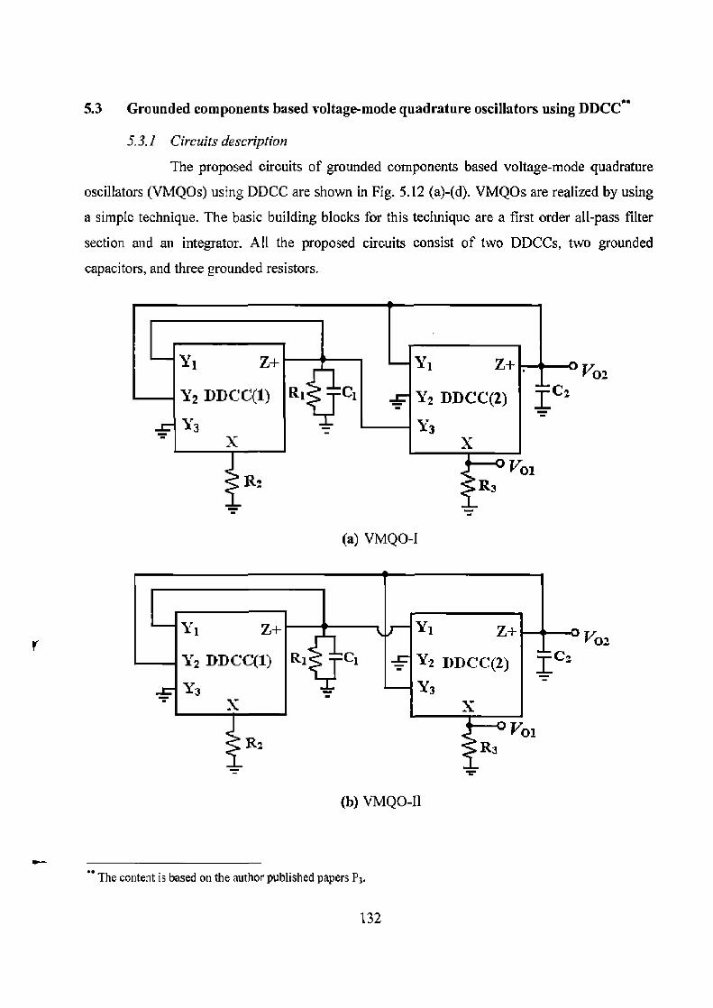
P3. J. Mohan, B. Chaturvedi, S. Maheshwari, "Grounded components based voltage-mode
quadrature oscillators", International Conference on Multimedia, Signal Processing and
Communication Technologies: IMPACT-2013, IEEE Doi: 978-1-4799-1205-6/13, pp. 241-
245, 2013.
P4. B. Chaturvedi, S. Maheshwari, "Current mode biquad filter with minimum component
count", Active and Passive Electronic Components, vol. 2011, pp. 1-7, 2011.
P5. S. Maheshwari and B. Chaturvedi, "Additional High Input Low Output Impedance Analog
Networks",Active and Passive Electronic Components, vol. 2013, Article ID 574925, 9
pages, 2013. (Doi:10.1155120131574925)
P6. B. Chaturvedi, S. Maheshwari, "Second order mixed mode quadrature oscillator using
DVCCs and grounded components", International Journal of Computer Applications, vol.
58, pp. 42-45, 2012.
P7. 3. Mohan, B. Chaturvedi, S. Maheshwari, "Novel current-mode all-pass filter with
minimum component count", International Journal of Image, Graphics and Signal
Processing, vol. 5, pp. 32-37, 2013.
P8. B. Chaturvedi, S. Maheshwari, "An ideal voltage mode all-pass filter and its applications",
Journal of Communication and Computer, vol. 9, pp. 613-623, 2012.
P9. B. Chaturvedi and S. Maheshwari, "Third-Order Quadrature Oscillator Circuit with Current
and Voltage Outputs", ISR.N Electronics, vol. 2013, Article ID 3 85062, 8 pages, 2013.
(Doi:10.1155/2013/385062)
P10. B. Chaturvedi, S. Maheshwari, "Cascadable band-pass filters using single active element
for low-Q applications", Chinese Journal of Engineering, 2013. (Communicated)
P11. B. Chaturvedi, S. Maheshwari, "Digitally controlled DXCC-II and its application",
International Journal of Circuit Theory and Applications, 2013. (Communicated)
,r
HIGH PERFORMANCE UNIVERSAL ACTIVE ELEMENTS FOR ANALOG SIGNAL PROCESSING
SUBMIT'TEDFOR THE AWARD_OF'T_FE,DEGREE
~ (\\'\\
OF
~~~' ' (f `~ • ~±L 'Pf;~ by { ~ .9 ~
AETa~csl. YEY3 (I /
(LJ i`fJ f f ! I
1~ ~1 \'rr A ~
~ ~~ ; ~7i BYE ~',_,';. •~ ~~ ,~~ rr r
B HART FJNiDcU=GH}AT,UIWE~DI
Under the Supervision of THESIS
DR. SUDHANSHU MAHESHWARI
DEPARTMENT OF ELECTRONICS ENGINEERING Z.H. COLLEGE OF ENGINEERING & TECHNOLOGY
ALIGARH MUSLIM UNIVERSITY ALIGARH (INDIA)
2013
1J, NOV 2014
(Dedt'cated:to
~FamiCy
certificate
It is certified that the Thesis entitled "HIGH PERFORMANCE UNIVERSAL ACTIVE
ELEMENTS FOR ANALOG SIGNAL PROCESSING". submitted by Mr. BHARTENDU
CHATURVEDI, for the award of the degree of DOCTOR OF PHILOSOPHY IN ELECTRONICS
ENGINEERING from Aligarh Muslim University, _Aligarh, .India is a record of candidate's
own work, carried out by him under my supervision. To the best of my knowledge, the
advances embodied in the Thesis have not been used-for..the award of any other degree.
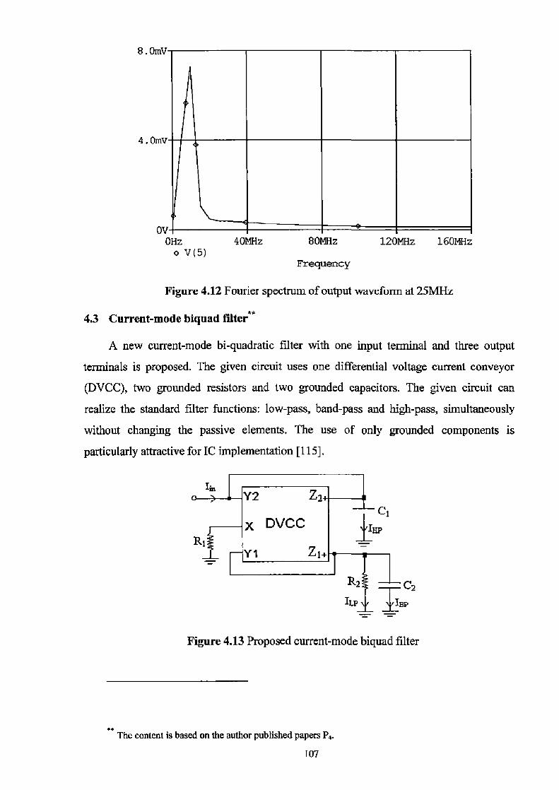
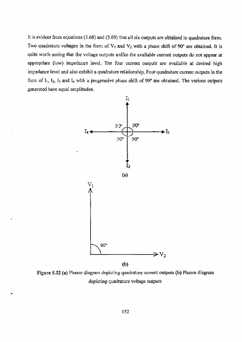
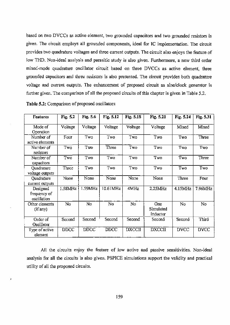
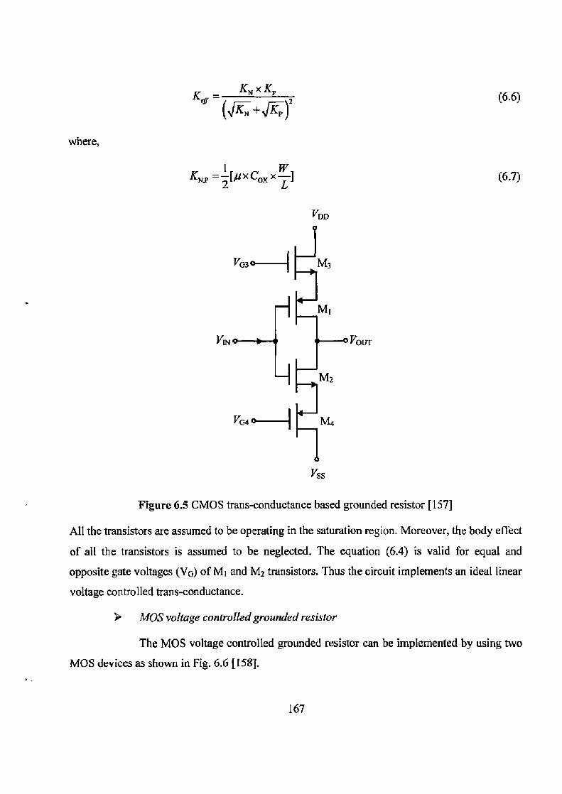
5.8 Conclusion 158 6. INTEGRATION AND TUNING ASPECTS 160
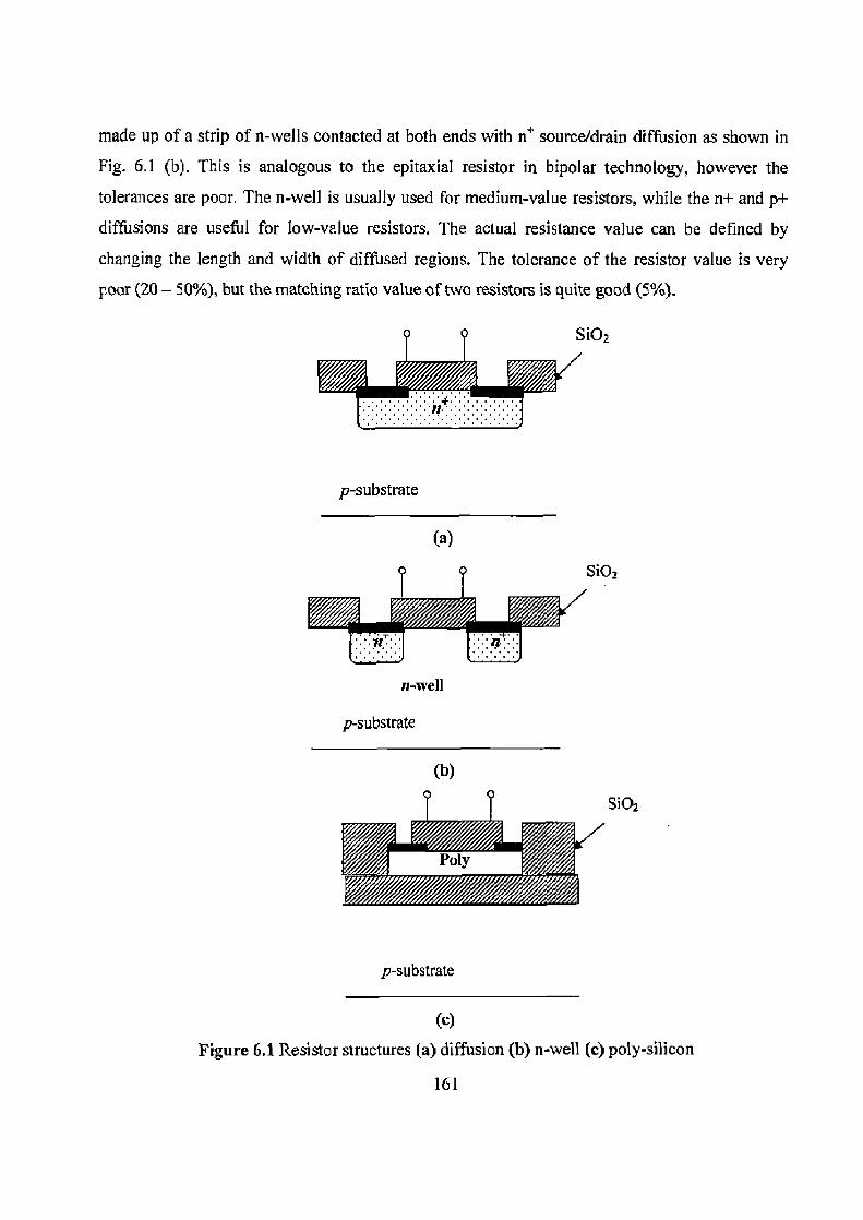
6.1 Resistors 160 6.2 Capacitors 162
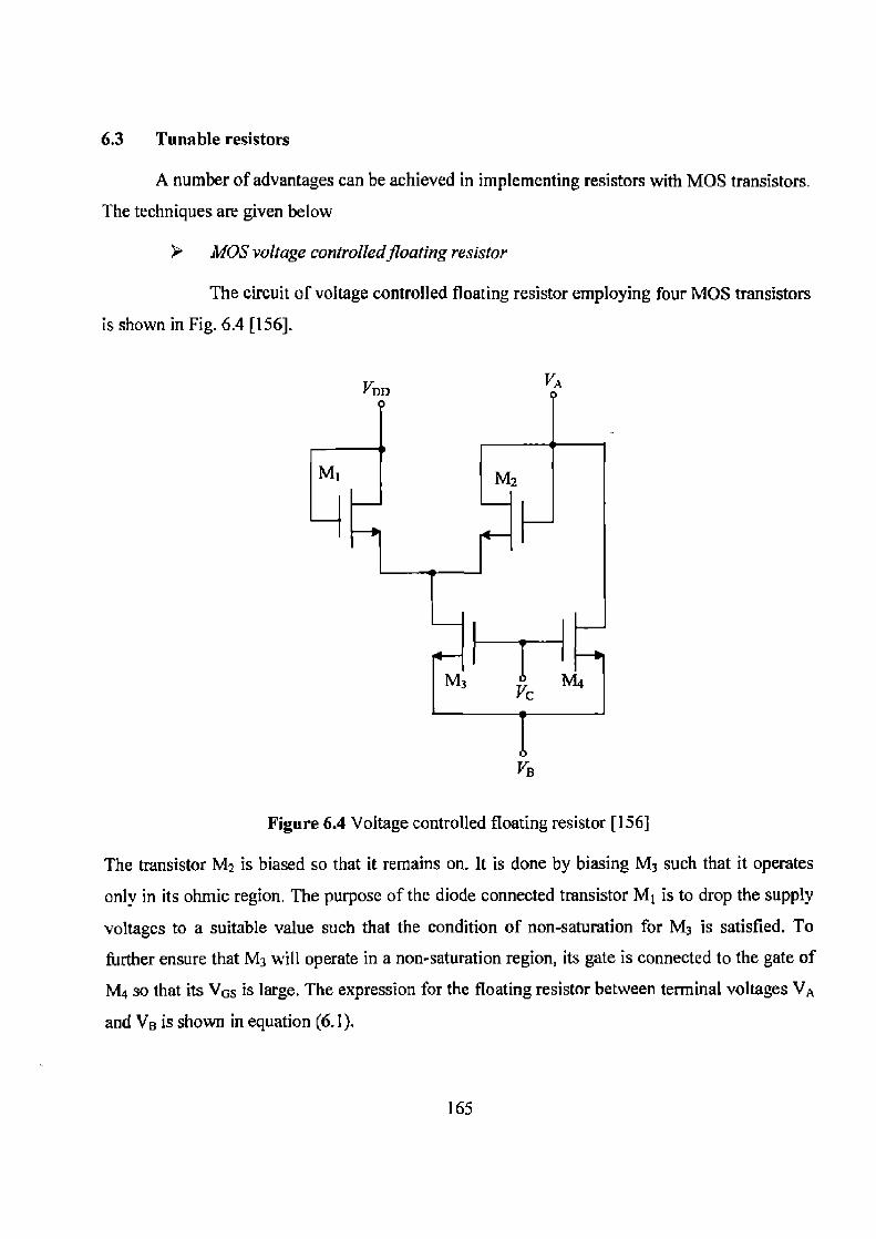
6.3 Tunable resistors 165
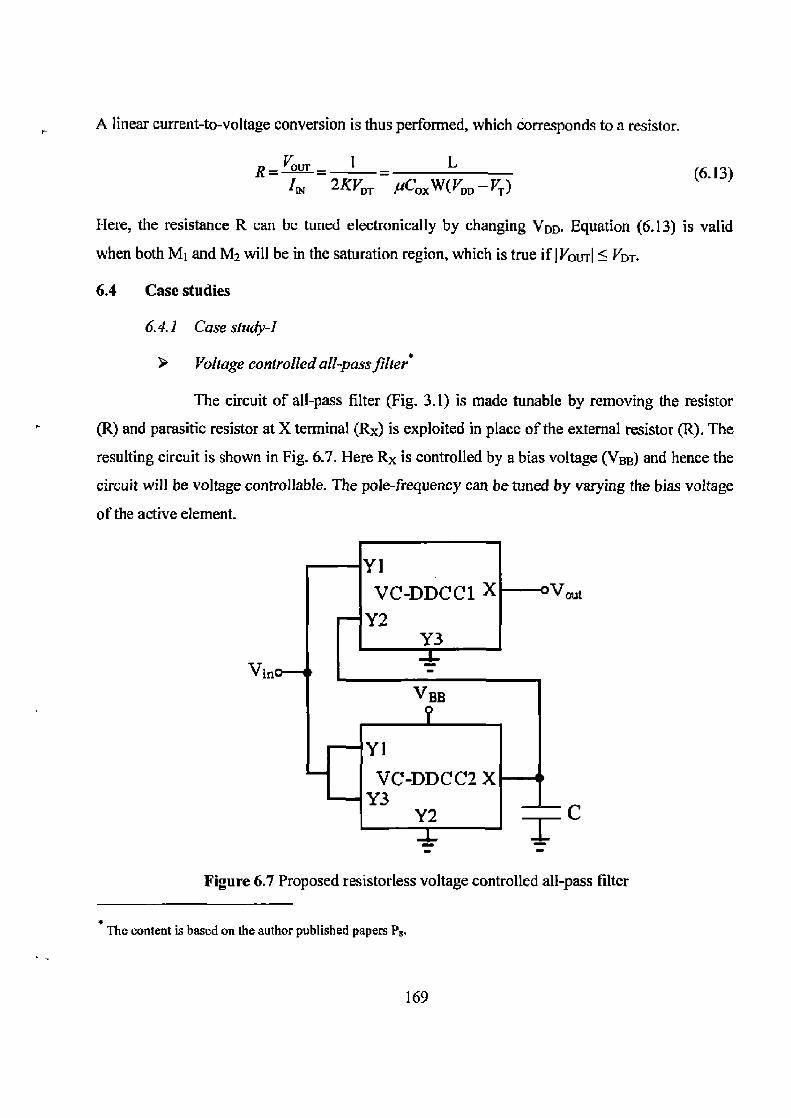
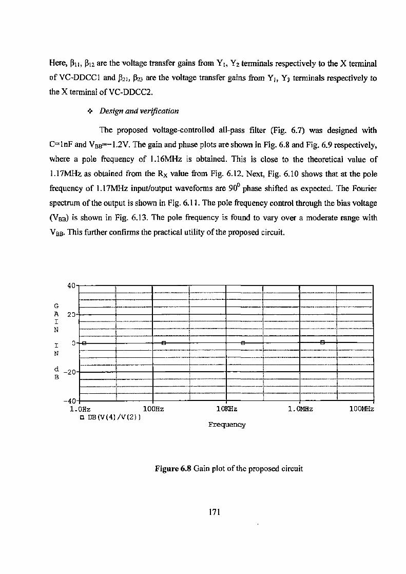
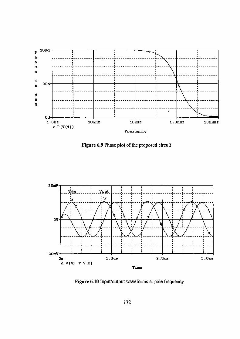
6.4 Case studies 169 6.4.1 Case study-I 169
6.4.2 Case study-11 173
6.4.3 Case study-III 176 6.4.4 Case study-IV 178
6.5 Concluding Remarks 181
7. CONCLUSION AND FUTURE SCOPE 182 7.1 Contribution to the Knowledge 182
7.2 Suggestions for future work 184
REFERENCES 185
XI
PUBLISHED PAPERS FROM THE THESIS
P1. S. Maheshwari, B. Chaturvedi, "High input low output impedance all-pass filters using one
active element", JET Circuits, Devices and Systems, vol. 6, pp. 103-110, 20I2.
P2. B. Chaturvedi, S. Maheshwari, "Simple voltage mode quadrature oscillator using CMOS
DDCC", International Conference on Multimedia, Signal Processing and Communication
Technologies: IMPACT-2011, IEEE Doi: 978-1-4577-7/11, pp. 220-223, 2011,
P3. J. Mohan, B. Chaturvedi, S. Maheshwari, "Grounded components based voltage-mode quadrature oscillators", international Conference on Multimedia, Signal Processing and
Communication Technologies: AIPACT-2013, IEEE Doi: 978-1-4799-1205-6/13, pp. 241-
245, 2013.
P4. B. Chaturvedi, S. Maheshwari, "Current mode biquad filter with minimum component
count", Active and Passive Electronic Components, vol. 2011, pp. 1-7, 2011.
P5. S. Maheshwari and B. Chaturvedi, "Additional High Input Low Output Impedance Analog
Networks", Active and Passive Electronic Components, vol. 2013, Article ID 574925, 9
pages, 2013. (Doi:10.115512013 /574925)
P6. B. Chaturvedi, S. Maheshwari, "Second order mixed mode quadrature oscillator using
DVCCs and grounded components", International Journal of Computer Applications, vol.
58, pp. 42-45, 2012.
P7. J. Mohan, B. Chaturvedi, S. Maheshwari, "Novel current-mode all-pass filter with
minimum component count", International 'Journal of Itnage, Graphics and Signal
Processing, vol. 5, pp. 32-37, 2013.
P8. B. Chaturvedi, S. Maheshwari, "An ideal voltage mode all-pass filter and its applications",
Journal of Corrnrrunication and Computer, vol. 9, pp. 613-623, 2012.
XI
P9. B. Chaturvedi and S. Maheshwari, "Third-Order Quadrature Oscillator Circuit with Current
and Voltage Outputs", ISRN Electronics, vol. 2013, Article ID 385062, 8 pages, 2013.
(Doi; 10.1155/2013/385062)
P10. B. Chaturvedi, S. Maheshwari, "Cascadable band-pass filters using single active element
for low-Q applications", Chinese Journal ofEngineering, 2013. (Communicated)
P11. B. Chaturvedi, S, Maheshwari, "Digitally controlled DXCC-II and its application",
International Journal of Circuit Theory and Applications, 2013. (Communicated)
3
LIST OF ABBREVIATIONS
AC Alternating Current
BiCMOS Bipolar Complementary Metal Oxide Semiconductor
CC Current Conveyor
CC-I First Generation Current Conveyor
CC-U Second Generation Current Conveyor
CC-III Third Generation Current Conveyor
CDBA Current Differencing Buffered Amplifier
CFA Current Feedback Amplifier
CFOA Current Feedback Operational Amplifier
clk Clock
CM Current-Mode
CMAPF Current-Mode All-Pass Filter
CMOS Complementary Metal Oxide Semiconductor
CO Condition Of Oscillation
dB Decibel
DC Direct Current
DDCC Differential Difference Current Conveyor
DDA Differential Difference Amplifier
DVCC Differential Voltage Current Conveyor
DXCC-II Dual X Second Generation Current Conveyor
FDCCII Fully Differential Second Generation Current Conveyor
FDNR Frequency Dependent Negative Resistance
Fig Figure
FO Frequency of Oscillation
IC Integrated Circuit
ICC-II Inverting Second Generation Current Conveyor
KCL Kirchhoff Current Law
MOS Metal Oxide Semiconductor
OP-AMP Operational Amplifier
OTA Operational Transconductance Amplifier
xiv
PSPICE Simulation Program with Integarted Circuit Emphasis
RC Resistor Capacitor
sin Sine Waveform
THD Total Harmonic Distortion
TSMC Taiwan Semiconductor Manufacturing Company
VC Voltage Controlled
VCVS Voltage Controlled Voltage Source
VLSI Very Large Scale Integration
VM Voltage-Mode
VMQO Voltage-Mode Quadrature Oscillator
xv
LIST OF SYMBOLS
a Non-ideal Current Transfer Gain
fj Non-ideal Voltage Transfer Gain
y Non-ideal Voltage Transfer Gain
E; Current Tracking Error
~v Voltage Tracking Error
0 Phase
H Gain
coo Pole or Angular Frequency
Degree
um Micrometer
p Mobility of Carriers
C Capacitance
Cox Gate Oxide Capacitance per Unit Area
Hz Hertz
ID Drain Current
I Current Flowing in the Transistor, MM
k Boltzmann Constant
K Transconductance Parameter Of The Transistor
MM CMOS Transistor
Q Quality Factor
R Resistance
C Capacitance
Cc Coupling Capacitance
xvi
L Inductance
L31, Simulated Inductance
g„r Transconductance
D Frequency Dependent Negative Resistance
CD Capacitance of the FDNR
S Sensitivity
s =jw Complex Parameter-Laplace Operator
I Current
V Voltage
VC Control Voltage
VBB Biasing Voltage
VDT, Vss Supply Voltages Of CMOS Structures
VDS Drain to Source Voltage
VAS Gate to Source Voltage
VG Gate Voltage
VT Threshold Voltage
W, L Channel Width and Length of CMOS Transistor
Z Impedance
% Percentage
S2 Ohm
KS~ Kilo Ohm
MI) Mega Ohm
pF Pico Farad
nF Nano Farad
VF Micro Farad
mH Mili Henry
xvii
mV Mili Volt
V Volt
µA Micro Ampere
mA Miii Ampere
A Ampere
MHz Mega Hertz
GHz Giga Hertz
LP Low Pass
HP High Pass
BP Band Pass
xviii
CHAPTER 1
INTRODUCTION
During the last many decades, analog and digital circuit designers considered voltages as the
most important circuit variable, although many of the signals encountered in circuits and systems
are actually currents in their initial state. The reason, why current signal processing was not able
to establish itself until now, was the missing high performance current processing circuits.
Although there are numbers of well established building blocks for voltage processing circuits,
e.g. operational amplifiers, comparators, etc., there was not enough attention paid to the design
of similar building blocks for current processing circuits.
A current conveyor belongs to the category of current processing building blocks. It is
very useful building block consisting of both voltage and current sub-blocks. Current conveyors
were introduced in the late sixties by Sedra and Smith. They were considered to be used as
controlled voltage and current sources, impedance converters, function generators, amplifiers,
filters etc. In the beginning of their appearance, the performance of current conveyors was
limited by the available technologies, which did not allow well-matched devices on fabricated
chips. Since the technologies have improved, the current processing blocks have also gained
attention of many analog designers. Today the current conveyors have developed to very useful
building blocks of analog signal processing and their main application areas are in high-speed,
high frequency circuits for both voltage-mode and current-mode signals.
1.1 Analog Signal Processing
Nowadays, the design of analog integrated circuits is an area of significance. As the
technology forges ahead, the performance/cost potential of the complete system cannot be fully
realized until integrated circuits with analog input and output can be implemented. Many new
high-performance devices have now been integrated with different advancements in IC
processing techniques. This in turn has led to a renewed interest in the analog circuit design
techniques. In the last decade, huge numbers of high performance devices were reported for this
purpose. An example is the development of "current-mode" techniques [1], many of which have
1
only become practically feasible with the development of true complementary bipolar and MOS
technology processes.
Voltage-mode analog circuit design is called a "traditional" nowadays. Current-mode
signal processing circuits have recently demonstrated many advantages over their voltage-mode
counterparts including higher bandwidth capability, greater Iinearity, higher operating speed and
wider dynamic range [1]. In addition, current-mode processing often leads to simpler circuitry
and lower power consumption. It is playing a significant role in the development of many new
high-performance circuits for signal processing application.
In the current scenario, CMOS VLSI is used to perform information processing more and
more in the digital area. However, the interface between the analog outside world and the digital
processor will continue to be analog in nature. Analog circuits are only competitive with digital
circuits in performance and area. Analog circuit design has historically been viewed as a voltage
dominated form of signal processing. Recently, current-mode analog circuits have emerged in
the implementation of analog functions. Due to many potential advantages [1-3], the current-
mode circuits have received considerable attentions as an alternative for signal processing
applications.
In CMOS technology, developments have centered on a new generation of analog
sampled data processing that may be referred to as switched or dynamic current circuits. These
circuits include switched current filters, dynamic current mirrors and memory cells. On the other
hand, novel special analog building blocks have been developed opposite to voltage-mode
classical blocks. These blocks, including current amplifiers, current followers, current conveyors
and others, can be called as "adjoint" to voltage amplifiers, voltage comparators, followers and
so on.
CMOS technology has become a dominant analog technology because of good quality
capacitors and switches. Furthermore with growing CMOS VLSI, current-mode analog design
techniques play an important role in successfully exploiting this technology in the analog
domain. As a consequence many of the early current-mode circuit techniques are enjoying a new
beginning and a new generation of current-mode analog building blocks and systems.
r
01
The advancement of the semiconductor technology in the last few decades had significant
impact to the research and development activities on electronic circuit and systems with
enormous coverage on analog signal processing. The impact had further renewed with
introduction of the versatile monolithic Integrated Circuit (IC) building block termed as
operational amplifier (op-amp) [2, 4]. The op-amp device is essentially a Voltage Controlled
Voltage Source (VCVS) element. Since its beginning, the op-amp element had been widely used
for various voltage mode circuit design covering widespread areas of applicabilities in analog
signal processing [2, 4]. Among these, the design of passive inductor-less active op-amp-RC
function circuits, e.g., integrators/differentiators, active filters, phase equalizers, wave generators
are quite popular, useful and IC-adaptable, since passive inductances are not compatible to IC
technology. The approach subsequently gave way to synthesize active immittance functions by
op-amp RC methods. During this track of research activity, Bruton suggested a new type of
immittance function known as the Frequency Dependent Negative Resistance (FDNR) [5]. In
this way of progress on analog signal processing circuit and system design, there emerged newer
types of active building block viz., the Operational Transconductance Amplifier (OTA) and the
Current Conveyor (CC), Many researchers had contributed elegant schemes on analog signal
processing circuit design using the OTA and the current conveyor in its various forms in the
recent past [1].
Recently, another new device, known as the Current Feedback Amplifier (CFA) had been
introduced, which is a versatile building block compatible to both voltage-mode and current-
mode functioning [1]. This is essentially a unity gain current transfer device wherein the voltage
across its trans-impedance can be copied at voltage source output nodes. The unique property of
the device is now commercially available as an off the shelf items as AD-844 IC. The CFA
element is receiving considerable interest on the R&D activities also in areas of analog signal
processing circuits [6, 7].
1.2 Historical perspectives
One of the most basic building blocks in the areas of current-mode analog signal
processing is the Current Conveyor (CC). It is a four (in basic form) terminal device which when
arranged with other electronic elements in specific circuitry can perform many useful analog
signal processing functions. In many ways current conveyor simplifies circuit design in current- 3
mode, in a manner similar to the conventional operational amplifiers (op-amp) in voltage-mode.
The current conveyor offers an alternative way of abstracting complex circuit functions, thus
aiding in the creation of new and useful implementations. Moreover, current conveyor is a
mixed-mode universal building block, which can substitute classical op-amps in voltage-mode
applications as well and provides an option to transform these applications to current-mode.
A lot of work has demonstrated the universality, advantages and novel applications of the
current conveyor since its first introduction in 1968 [8]. Concurrently with these works, a
number of researchers have outlined improved implementations designed to enhance the
performance and utility of this building block. Some existing current conveyors are discussed
below.
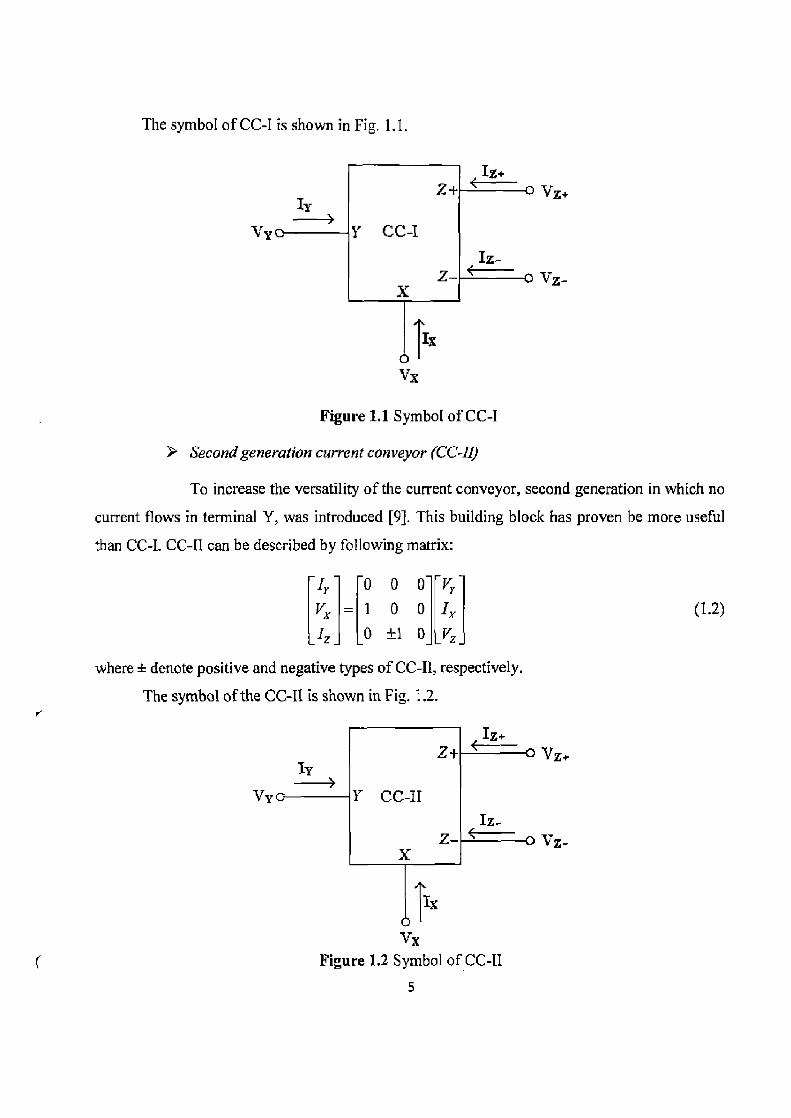
D First generation current conveyor (CC-1)
The current conveyor was originally introduced as 3-port device [8]. The
operation of this device can be described as: if a voltage is applied to input terminal Y, an equal
potential will appear on the input terminal X. In a similar fashion, an input current being forced
into terminal X will result in an equal amount of current flowing into terminal Y. Finally, the
current flowing into terminal X will be conveyed to output terminal Z. Note that Z output
terminal has characteristics of a current source with high output impedance. Voltage at X
terminal is independent on the current forced into this port. Similarly, the current flows through
input Y is fixed by current through X terminal and is independent on Y potential. The
functionality of CC-I can be described by following matrix;
ly 0 1 0 VI - 1 0 0 Ix I2 0 ±1 0 VZ
where ± denote positive and negative types of CC-1, respectively.
4
I
The symbol of CC-I is shown in Fig. I.I.
zY Vy Y CC-I
Iz_ z-- ±— V. a-
X
Ix
Figure 1.1 Symbol of CC-I
➢ Second generation current conveyor (CC-If)
To increase the versatility of the current conveyor, second generation in which no
current flows in terminal Y, was introduced [9]. This building block has proven be more useful
than CC-I. CC-II can be described by following matrix:
f,. 0 0 0 Vr Vx = 1 0 0 IX (1.2) IZ 0 ±1 0 Vz
where ± denote positive and negative types of CC-II, respectively.
The symbol of the CC-II is shown in Fig. 1.2.
Iz+
Iv
Y CC-II I.
(_-0 V z- x
T1C
Figure 1.2 Symbol of CC-II 5
r
From equation (1.2), it is clear that terminal Y exhibits infinite input impedance. The voltage at
X terminal follows the voltage of Y terminal, X exhibits zero input impedance, and current flows
through X port is conveyed to the high impedance output terminal Z. Current flows through Z
terminal with same orientation as current through the terminal X (CCII+) or opposite polarity in
case of CCII-. CC-II has proven to be considerably more useful type of the current conveyor
family. Wide range of applications was reported. It is very suitable building block for design of
the active-RC filters or number of special immittance (admittance) or/and simulators. CC-II is
also used as a powerful building block for low voltage applications.
➢
Third generation current conveyor (CC-Ill)
Current conveyor-III was reported in 1995 [10]. The operation of the third
generation current conveyor (CC-III) is similar to that of the first generation of current conveyor
(CC-i), with the exception that the currents in ports X and Y flow in opposite directions (A= -1).
As the input current flows into the Y-terminal and out from the X terminal, the CC-III has high input
impedance with common-mode current signals, i.e. identical currents are fed both to Y and X terminals.
Therefore common-mode currents can push the input terminals out from the proper operation range.
Therefore this conveyor is used as current probing. CC-III can be described by following matrix:
_TY o —1 d VY
VX = 1 0 0 IX (1.3)
L' ] 4 ±1 oiLi VZ where ± denote positive and negative types of CC-III, respectively.
The symbol of CC-III is shown in Fig. 1.3.
Iz}
Z+ Vz~ Iy
V' Y CC-III Iz-
Z— ~! Vz- x
Figure 1.3 Symbol of CC-III 6
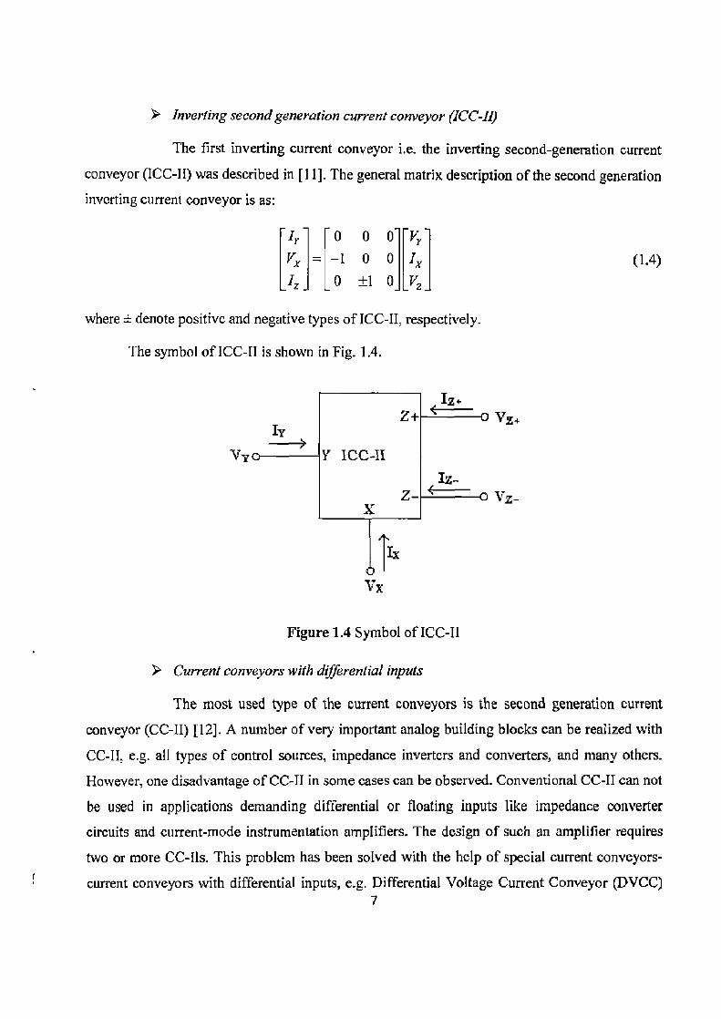
➢ Inverting second generation current conveyor (ICC-II)
The first inverting current conveyor i.e. the inverting second-generation current
conveyor (ICC-II) was described in [11]. The general matrix description of the second generation
inverting current conveyor is as:
Ir 0 0 0 VY VX _ —1 0 0 I X IZ 0 ±1 0 Vz
where th denote positive and negative types of ICC-II, respectively.
The symbol of ICC-II is shown in Fig. 1.4.
TZ+
IY
Vy 4 ICC II
I2_
IX
VX
Figure 1.4 Symbol of ICC-TI
Current conveyors with differential inputs
The most used type of the current conveyors is the second generation current
conveyor (CC-II) [12]. A number of very important analog building blocks can be realized with
CC-II, e.g. all types of control sources, impedance inverters and converters, and many others.
However, one disadvantage of CC-II in some cases can be observed. Conventional CC-II can not
be used in applications demanding differential or floating inputs like impedance converter
circuits and current-mode instrumentation amplifiers. The design of such an amplifier requires
two or more CC-Ils. This problem has been solved with the help of special current conveyors-
current conveyors with differential inputs, e.g. Differential Voltage Current Conveyor (DVCC) 7
(1.4)
[ 13], Differential Difference Current Conveyor (DDCC) J14] etc. The DVCC and DDCC are
relatively simple and useful building blocks, which keep all advantages of CC-II and cancel the
disadvantage of single high-impedance input terminal.
In this section a number of current conveyor types were presented. Some of them could
become powerful functional building blocks for monolithic ICs.
1.3 State-of-the-Art
Research in analog integrated circuits has recently gone in the direction of low-voltage
and high-speed design, especially in the environment of the portable systems where a low supply
voltage, given by a single-cell battery, is used. In this area, traditional voltage-mode techniques
are going to be substituted by the current-mode approach, which has to be advantageous to
overcome the gain-bandwidth product limitation, typical of operational amplifiers. Inside the
current-mode architectures, CC-II can be considered as basic circuit block because all active
devices can be made of a suitable connection of one or two CC-IIs. CC-II is particularly
attractive in portable systems, where low voltage constraints have to be taken into account. In
fact it suffers less from the limitation of low current utilization, while showing full dynamic
characteristics at reduced supplies (especially CMOS versions) and good high frequency
performance. Recent advances in integrated circuit technology have also highlighted the
usefulness of CC-ll solutions in large number of signal processing applications.
In the present days a number of trends can be noticed in the area of analog filter and
oscillator design, namely reducing the supply voltage of integrated circuits and transition to the
F current-mode [1]. On the other hand, voltage-mode and mixed-mode circuit design still receives
considerable attention of many researchers. Therefore, the proposed circuits in this Thesis are
working in current-mode or voltage-mode or mixed-mode.
1.4 Organization of the Thesis
The Thesis is elaborated in seven chapters. The organization of this Thesis is described
below.
Chapter 2 starts with the overview of active devices namely Differential Voltage Current
Conveyor (DVCC), Differential Difference Current Conveyor (DDCC), Voltage Controlled-
0
Differential Difference Current Conveyor (VC-DDCC) and second generation Dual-X Current
Conveyor (DXCC-II) along with their CMOS implementation. Detailed performance study and
device verification are also given. This chapter further proposes DXCC-II with buffered output
and Digitally Controlled DXCC-II (DC-DXCCII) with buffered output. Implementation of
DXCC-II with buffered output and DC-DXCCII with buffered output in CMOS technology
along with non-ideal study and simulation results is also proposed. These active building blocks
are further used in Thesis for the realization of various applications.
Chapter 3 proposes different novel first order all-pass sections. Firstly, a new circuit of
first order voltage-mode all-pass filter using DDCC is proposed. Eight new first order voltage-
mode all-pass filters based on new proposed topologies are also included. Finally, two novel first
order current-mode all-pass filters employing a single DXCC-I1 are proposed. All the circuits
possess appropriate impedance levels.
Chapter 4 is focused on the design of new second order filters. Firstly, two all-pass filters
based on simulated inductor are proposed. Floating simulators have been employed to overcome
the drawbacks of passive inductors. Next, two circuits of all-pass filter using frequency
transformation are proposed. Transformation technique has been also employed in this chapter to
realize simpler alternative with lesser circuit complexity. Furthermore, a new second order
current-mode filter circuit employing grounded components is proposed. The circuit uses a
minimum number of components required to achieve a second order transfer function. Three
types of transfer functions are available at once, without any circuit modification. In the last,
-r
single active element based two new second order band-pass filters with the feature of high input
and low output impedance are proposed. Both the circuits are simple and contain a minimum
number of active components required to achieve a second-order transfer function. The proposed
circuits benefit from low active and passive sensitivities. Although the proposed circuits are
designed for low-quality factor property, they can be used for cascading in different applications
at high frequency also. Extensive simulations are performed to validate the proposed theory.
Chapter 5 deals with several new oscillator circuits. Most of the proposed circuits are
simple and contain a minimum number of components required to achieve quadrature
oscillations or multi phase oscillations. All the circuits enjoy the feature of low active and
passive sensitivities. P7
Chapter 6 explores the integration and tuning aspects. The passive elements in form of
resistors and capacitors can also be made compatible in CMOS technology. This chapter
discusses the fabrication possibilities of these passive components in CMOS technology. This
chapter further presents case studies whereas tunability aspects of some of the circuits are
studied.
In Chapter 7, conclusions are drawn and the original contributions of this Thesis are
summarized. Finally suggestions for further research are given.
The non-ideal analysis as well as the effects of parasitics is also included to complete the
study of performance of the all proposed circuits. All the proposed circuits are designed and
simulated using PSPICE. One experimental setup is also given for presentation of the results.
10
CHAPTER 2
UNIVERSAL ACTIVE ELEMENTS
Second-generation current conveyors (CCIIs) [12] have been found very useful in many
applications. This is attributed to their higher signal bandwidths, greater linearity, and larger
dynamic range than those of the operational-amplifiers (op-amps) based ones. Ever since its
introduction, many modifications have been made to increase the versatility of the active
element, such as differential voltage current conveyor (DVCC) [13], differential difference
current conveyor (DDCC) [14], dual X current conveyors (DXCC-II) [16] etc. In the most
modern high performance analog integrated circuits, differential circuits are needed since it
improves the performance of analog systems in terms of noise rejection, dynamic range through
the cancellation of even harmonics, as well as to suppress the effect of coupling between various
blocks. DVCC, DDCC and DXCC-II are versatile active elements which can simplify the design
of active networks. Most of the active elements named above (CC-II, DVCC/DDCC etc.) can be
called universal in the sense that these can be used stand alone to realize several other current-
mode active elements being used and introduced in literature.
This chapter includes the brief introduction of DVCC, DDCC, VC-DDCC, DXCC-II,
DXCC-II with buffered output and DC-DXCCII. In section 2.1, implementation of DVCC in
CMOS technology is given. In section 2.2, CMOS implementation of DDCC is presented. VC-
DDCC is discussed in section 2.3. The CMOS implementation of DXCC-Ii is presented in
section 2.4. Furthermore, two new active elements are proposed. In section 2.5, implementation
of DXCC-II with buffered output in CMOS technology along with non-ideal study and
simulation results is proposed. In section 2.6, CMOS implementation of DC-DXCCII is
proposed. This chapter also presents the PSPICE simulated results for all active elements, which
verifies the dc, ac and transient behavior of these universal active elements.
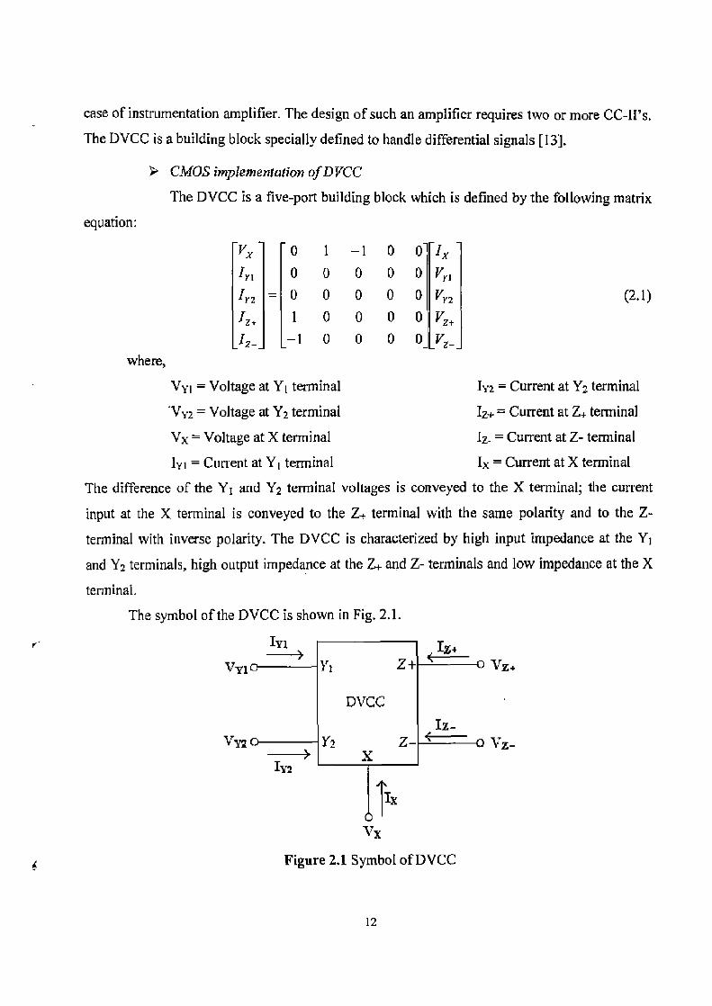
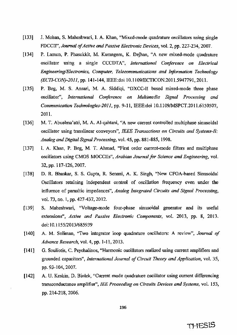
2.1 Differential Voltage Current Conveyor (DVCC)
The Differential Voltage Current Conveyor (DVCC) is an extension of the second-
generation current conveyor (CC-ll) introduced by Sedra and Smith [12]. The CC-II has a
disadvantage that only one of input terminals has high input impedance (Y terminal). This
disadvantage becomes evident when CC-II is required to handle differential signals, as in the
11
case of instrumentation amplifier. The design of such an amplifier requires two or more CC-II's.
The DVCC is a building block specially defined to handle differential signals [13].
➢ CMOS implementation of DVCC
The DVCC is a five-port building block which is defined by the following matrix
equation:
VX 1 r 0 1 —1 0 0 I X 'Y , 0 0 0 0 0 v~, 'Y2 = 0 0 0 0 0 VY2 (2.1)
Iz} 1 0 0 0 0 VZ+
IZ_ —I 0 o 0 0 Vz_ where,
VY1= Voltage at Yi terminal IY2 = Current at Y2 terminal
'VY2 = Voltage at Y2 terminal Iz+ = Current at Z+ terminal
Vx = Voltage at X terminal Iz_ = Current at Z- terminal
lyi = Current at Yi terminal Ix = Current at X terminal
The difference of the Y1 and Y2 terminal voltages is conveyed to the X terminal; the current
input at the X terminal is conveyed to the Z,. terminal with the same polarity and to the Z-
terminal with inverse polarity. The DVCC is characterized by high input impedance at the Y1
and Y2 terminals, high output impedance at the Z+ and Z- terminals and low impedance at the X
terminal.
The symbol of the DVCC is shown in Fig. 2.1.
r IY1 IZ+
VYl 7['i
DVCC zZ_
VY2 0 Y2 z- 0 Vrj-
1Y2x
z
TIX
A'x
Figure 2.1 Symbol of DVCC
12
VI
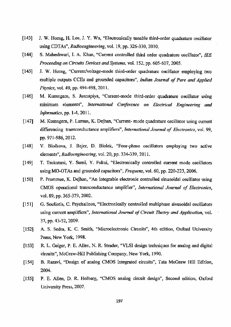
The DVCC is a versatile building block for applications demanding floating inputs. The CMOS
implementation of the DVCC [13] is shown in Fig. 2.2.
Vss
Figure 2.2 CMOS implementation of DVCC [13]
All transistors operate in saturation region and the sources are connected to bulk/substrate.
Transistors M5 and M6, work as a current mirror which are set to drive two differential
amplifiers consisting of transistors MI, M2 and M3, M4 respectively. Transistors M7 and MI4
provide the necessary feedback action to make the voltage Vx independent of current drawn
from the terminal X. The current through terminal X is conveyed to the Z+ terminal with the help
of transistors M7, M8, M14 and M15. By using extra current mirror the current is conveyed in an
inverted manner to the Z- terminal.
➢ Non-ideal analysis
Taking the non-idealities of the DVCC into account, the relationship of the
terminal voltages and currents of the DVCC can be rewritten as:
13
Vx 0 flkt — )3k2 0 0 I X 'Y, 0 0 0 0 VY,
Ire 1=1 0 0 0 0 0 VY2 1 (2.2)
1z► aki 0 0 0 0 Yz+ z_ — c k2 0 0 0 0 Vz-
where, /3k/(S), flu(s) represent the frequency transfers of the internal voltage followers and akf(s), ak2(s) represent the frequency transfers of the internal current followers of the kth-DVCC,
respectively. If DVCC is working at frequencies much less than the corner frequencies of/3k!(s),
/3k2(s), akl (s) and ak2(s), namely, then /iki(s) = uk1=1-ckv f where, sk,j (Ick„!J <<I) denotes the
voltage tracking error from the Y, terminal to the X terminal of the kth—DVCC; /3k2(s) = &2=I-
EL-v2 where, ah 2 (k 2I <<1) denotes the voltage tracking error from the Y2 terminal to the X
terminal of the kth—DVCC; akl(s) = aki =1-aklr where, E f (Ieki1f <<1) denotes the current tracking
error from the X terminal to the 7.+ terminal and ak2(s) = ak2 =1-sk,2 where, 2k12 (Is. 2[ «l) denotes
the current tracking error from the X terminal to the Z- terminal of the kth—DVCC.
➢ Parasitic effects
The parasitic model of DVCC is shown in Fig. 2.3. It is shown that the real
DVCC has parasitic resistors and capacitors at port Z in form of R7JICz, at port Y in form of
Ry//Cy and at port X parasitic are in form of series combination of resistance Rx and capacitor
Cx. Ideally, the DVCC is used at frequencies much lower than the corner frequencies of a; (i=1,
2) and J3 (i=l, 2). For typical applications built around DVCC, the external resistors (R) are
much smaller than the parasitic resistors at the Y and Z terminals of DVCC, i.e. R<<Ry or RZ
and the external resistors are much greater than the parasitic resistor at the X terminal of DVCC,
i.e. Rx<<R. IYi Iz+ _____
dry] Sri = Cyl [ Rvt Z+_C=.1] Rz.
DVCC
VYZ Y2 Z- __ ZY2 = CY21 [ Rra
ThEE!
cx Figure 2.3 Parasitic model of DVCC
14
> Simulation results
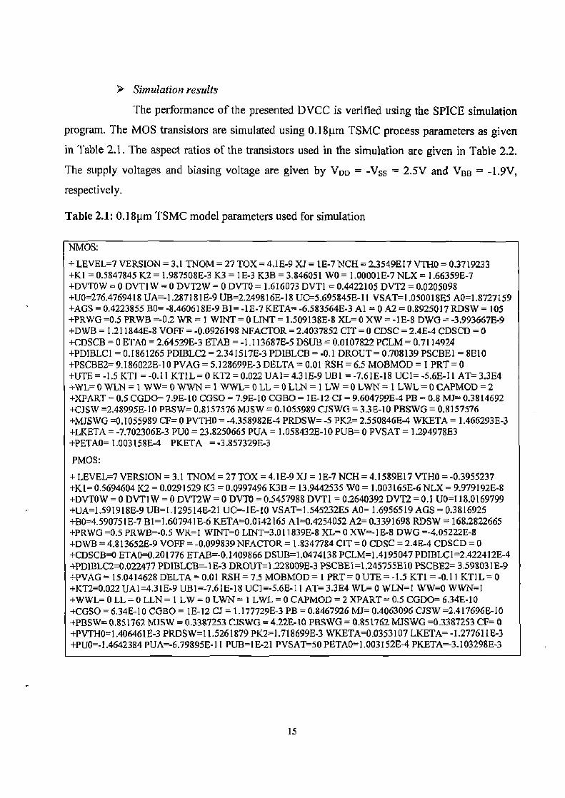
The performance of the presented DVCC is verified using the SPICE simulation
program. The MOS transistors are simulated using 0.18µm TSMC process parameters as given
in Table 2.1. The aspect ratios of the transistors used in the simulation are given in Table 2.2.
The supply voltages and biasing voltage are given by VDD = -VS5 = 2.5V and VBB = -1.9V,
respectively.
Table 2.1: 0.18µm TSMC model parameters used for simulation
VYi = Voltage at Yi terminal IY2 = Current at Y2 terminal
VYZ = Voltage at Y2 terminal IY3 = Current at Y3 terminal
VY3 = Voltage at Y3 terminal Iz+ = Current at Z+ terminal
VX = Voltage at X terminal IZ_ = Current at Z. terminal
Iy = Current at Yl terminal Ix = Current at X terminal
The difference of the Yi and Y2 terminal voltages in addition with the voltage at Y3 terminal is
conveyed to the X terminal; the current input at the X terminal is conveyed to the Z+ terminal
with the same polarity and to the Z- terminal with inverse polarity. In a DDCC, terminals Y1, Y2
and Y3 exhibit infinite input impedance. Thus, no current flows in terminals Y1 , Y2 and Y3. The
terminal X exhibits zero input impedance. The terminals Z+ and Z- have infinite output
impedance.
The symbol of the DDCC is shown in Fig. 2.17.
I-1
i Yt y1 IZ+ IY2 I Z+ ^
VY2 ' y2 DDCC
Figure 2.17 Symbol of DDCC 5
23
1
11
Y2
V
The CMOS implementation of the DDCC [14] is shown in Fig. 2.18. -tT
Vss
Figure 2.18 CMOS implementation of DDCC [14]
All transistors operate in saturation region and the sources are connected to
bulk/substrate. Transistors M5 and M6, work as a current mirror which are set to drive two
differential amplifiers consisting of transistors M1, M2, M3 and M4. Transistors M7 and M14
provide the necessary feedback action to make the voltage Vx independent of current drawn
from the terminal X. The current through terminal X is conveyed to the Z+ terminal with the help
of transistors M7, M8, M14 and M15. By using extra current mirror the current is conveyed in an
inverted manner to the Z- terminal.
Non-ideal analysis
Taking the non-idealities of the DDCC into account, the relationship of the terminal
voltages and currents of the DDCC can be rewritten as
24
VX 0 )9ki — )'k2 Pk3 0 0 -[x In 0 0 0 0 0 0 Vri 'V2 0 o o o o 0 VY2 IY3 - 0 0 0 0 0 0 VY3
(2.4)
1z+ aki 0 0 0 0 0 v IZ- -a 0 0 0 0 0 yZ-
where, Jikl(s), 13k2(s) and &3(s) represent the frequency transfers of the internal voltage followers
and akl(s), ak2(s) represent the frequency transfers of the internal current followers of the kth-
DDCC, respectively. If DDCC is working at frequencies much less than the corner frequencies
of flkr(s),13kz(S), 603(s), akJ(s) and ak2(s), namely, then /kl(s) =fikr=I -E,! where, Ems► (Ic wI <<1) denotes the voltage tracking error from the Y1 terminal to the X terminal of the kth—DDCC;
= fik2=1 where, Fh2 (IEk,21 <<1) denotes the voltage tracking error from the Y2 terminal
to the X terminal of the kth—DDCC; Qkj(s) = f k3= I -ck,3 where, Ekv3 (Is3I <<1) denotes the voltage
tracking error from the Y3 terminal to the X terminal of the kth—DDCC; ak,(s) = ak; =1- j
where, sk,f (Iski4 <<I) denotes the current tracking error from the X terminal to the Z{ terminal
and ak2(s) ak2 =I-Eki2 where, sk j2 (1c,42I <<1) denotes the current tracking error from the X
terminal to the Z- terminal of the kth—DDCC.
Parasitic effects
The parasitic model of DDCC is shown in Fig. 2.19. It is shown that the real
DDCC has parasitic resistors and capacitors at port Z in form of Rz//CZ, at port Y in form of
Ry/ICy and at port X parasitic are in form of series combination of resistance Rx and capacitor
C. Ideally, the DDCC is used at frequencies much lower than the corner frequencies of a1 (i=l,
2) and f (i=1, 2, 3). For typical applications built around DDCC, the external resistors (R) are
much smaller than the parasitic resistors at the Y and Z terminals of DDCC, i.e. R<<Ry or Rz
and the external resistors are much greater than the parasitic resistor at the X terminal of DDCC,
i.e. RX<<R.
25
`Y1 Cyi I I RYl IY2
Y2
Z12 .. CY2IIRy2 IY3
Vy3
zy3 - cY3 I I RY3
1
2 DDCC
x
Rx
IZ+
Z =Cz+I! R .~
u- z- '
ZC I Rz
Figure 2.19 Parasitic model of DDCC
Simulation results
The performance of the presented DDCC is verified using the SPICE simulation
program. The MOS transistors are simulated using 0.18µm TSMC process parameters and are
given in Table 2.3. The aspect ratios of the transistors used in the simulation are given in Table
2.4. The supply voltages and biasing voltage are given by VDD = -V5s = 2.5V and VBB = -1.6V,
respectively.
Table 2.3: 0.18im TSMC model parameters used for simulation
Figure 2.48 Input/output voltages at Y, X 1- and X- terminals
46
-2 OOuk Os n I (Rl)
2 0 QuA-
OA-
5us lOus v 1(VZp)
Time
15us 20us
2OOuZ
DA
Figure 2.49 Input/output currents at X+ and Z+ terminals
II .. ii I;IiI - - --
Figure 2.50 Input/output currents at X- and Z- terminals
-200uA Os o '(R2)
5us lOus l5us 20us G I(VZfl)
Time
47
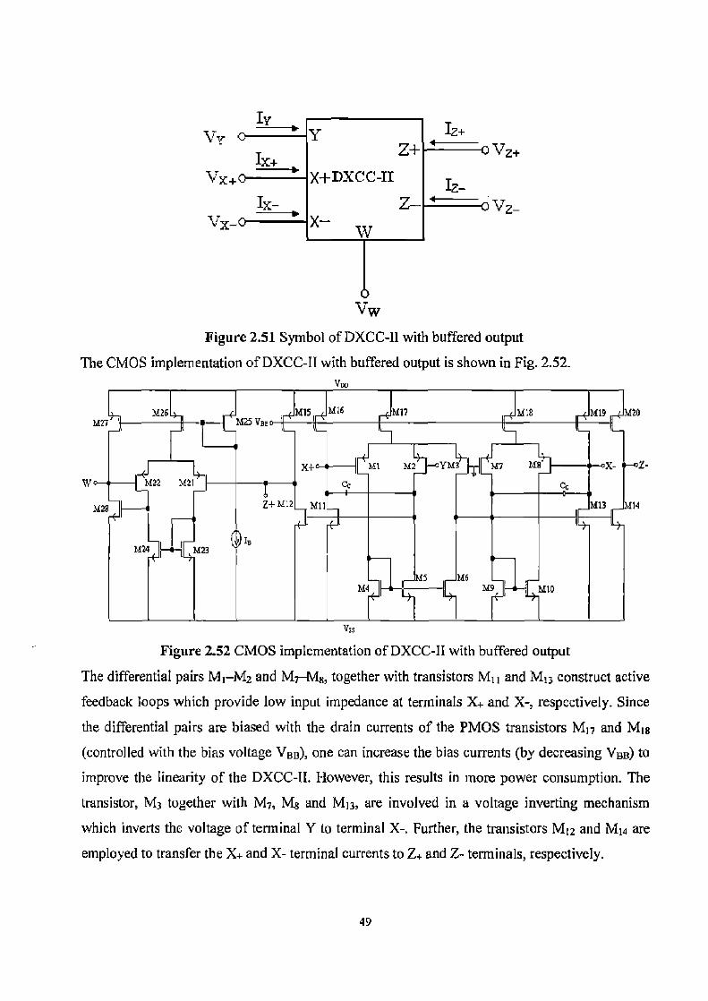
2.5 Proposed Dual X Current Conveyor-II (DXCC-II) with buffered output*
The DXCC-I1 with buffered output is a combination of regular DXCC-II and a buffer. It
has one extra low impedance terminal, which is needed for voltage-mode applications.
2.5.1 CMOS implementation of DXCC-II with buffered output
The DXCC-II with buffered output is also a five-port building block which is
defined by the following matrix equation:
VX* 0 0 1 0 a iX+
VX - 0 0 —1 0 0 II IX-
I VW 0 0 0 1 0
i = 0 0 0 0 0 YY I (2.8) IIz+i 1 0 0 0 0
II Vz+ I
Lz-] p 1 0 a s Yz
where,
Vv = Voltage at Y terminal
Vx+ = Voltage at X+ terminal
V x_ = Voltage at X- terminal
Vw = Voltage at W terminal
Iy = Current at Y terminal
Iz+ = Current at Z+ terminal
IZ_ = Current at Z. terminal
Ix± = Current at X1- terminal
Ix- = Current at X- terminal
The symbol of DXCC-II with buffered output is shown in Fig. 2.51. The DXCC-II with
buffered output has several terminals as follows:
• One high input impedances voltage input terminals: Y
• Two low impedance current input terminal: X+, X-
• Two high impedance current output terminals: Z+, Z-
• One low impedance voltage output terminal: W
The content is based on Author published paper Pt.
48
Zy Vy Y IZ+
Ix+ Z+ VZ+
'x+ I- X+DXC'C -II IZ-
Ix~ Z- '
V
Figure 2.51 Symbol of DXCC-II with buffered output
The CMOS implementation of DXCC-II with buffered output is shown in Fig. 2.52. VDD
W.
VSS
Figure 2.52 CMOS implementation of DXCC-II with buffered output
The differential pairs M, M2 and M7—M8, together with transistors M„ and M13 construct active
feedback loops which provide low input impedance at terminals X+ and X-, respectively. Since
the differential pairs are biased with the drain currents of the PMOS transistors M17 and M18
(controlled with the bias voltage VBB), one can increase the bias currents (by decreasing VaB) to
improve the linearity of the DXCC-II. However, this results in more power consumption. The
transistor, M3 together with M7, M8 and M13, are involved in a voltage inverting mechanism
which inverts the voltage of terminal Y to terminal X-. Further, the transistors M12 and M14 are
employed to transfer the X+ and X- terminal currents to Z+ and Z- terminals, respectively.
k.
Transistors M21 to M28 with a bias current Ia combinely form a buffer, which provides
one extra low impedance terminal W. The voltage at Z+ terminal is equal to the voltage at
terminal W.
2.5.2 Non-idealities
Taking the non-idealities of the DXCC-II into account, the relationship of the
terminal voltages and currents of the newly developed DXCC-1I can be rewritten as
0 0 'ski 0 0 Tex+ Vx- 0 0
Ix- Vw 0 0 0 yk 0 Ir 1 — 0 0 0 0 0 VY (2.9)
Iz+ aki 0 0 0 0 vz+
Iz - a ak1 0 o o yZ-
where, J3*j(s), /3k2(s) and yk(s) represent the frequency transfers of the internal voltage followers
and aki(s), ak2(s) represent the frequency transfers of the internal current followers of the kth-
DXCC-II, respectively. If the DXCC-II is working at frequencies much less than the corner
frequencies of flkf(s), #0(S), yk(s), ak,(s) and ak2(s), namely, then flk,(s) _ /3k1= I -c -j where, cl
(Ic ,iI «I) denotes the voltage tracking error from the Y terminal to the X+ terminal of the kth-
DXCC-II; /3,u(s) = flk2=1-sk,,2 where, EA-2 (IEki21 <<I) denotes the voltage tracking error from the Y
terminal to the X- terminal of the kth—DXCC-II; yk(s) = yk=l-&kwhere, sk„ (IEt <<I) denotes the
voltage tracking error from the Z terminal to the W terminal of the kth—DXCC-II; a ,(s) = ak!
=1-cka1 where, ckri (] I «I) denotes the current tracking error from the X+ terminal to the Z+
terminal; and 1(s) = ak2 =I-skr2 where, sk,2 (lEki2I <<1) denotes the current tracking error from the
X- terminal to the Z- terminal of the kth—DXCC-II.
2.5.3 Simulation results
The performance of the proposed DXCC-II with buffered output is verified using
the SPICE simulation program. The simulations are based on 0.1811m TSMC CMOS parameters.
The supply voltages used are f2.5V, VBB = -1.55V, Cc = 0.06pF and In = 25µA. The newly
developed DXCC-II with buffered output exhibits low output impedance at W which was
measured and found as 1851).
so
• DC analysis
DC analysis has been done to verify the current and voltage relationships
separately. Fig. 2.53 to Fig. 2.58 show the DC characteristic of DXCC-II with buffered output.
Fig. 2.53 shows that when DC voltage of 50mV is applied at input terminal Y then DC voltage of
50mV is available at terminal X+ and DC voltage of -50mV is available at terminal X-. lOOrnV--- - - ____
-lOOmV• OS a V(1)
ov.
V Y
V -'----
4-- .- - 4i.is Bus l2us 16us 20us
o V(2) v V(3)
q
Time
Figure 2.53 Verification of input voltages (Vx++Vy and V+-Vy)
Fig. 2.54 shows that the voltage at W terminal (Vw) is same as the voltage at Z+ terminal (Vz+).
Therefore, Fig. 2.53 and Fig. 2.54 verify the relationship of voltages of equation (2.8).
-p:— - - - - ----
5us lOus 15us 20us
Time
Figure 2.54 Verification of output voltages (VwVz+)
10 Cmv
5 Cmv
0v. Os n V(4) o V(6)
51
—lOOmV- 11 M
—10 0irU! o V(6)
lOOmV•
Dv.
II:IIIIIIIIIII
—5OmV Dv 50mV lOOmS!
4.
Fig. 2.55 shows the variation in voltages at X, terminal (V +) and X- terminal (Vx-) against the
input voltage at Y terminal (Vy). Fig, 2.56 shows the variation in voltage at W terminal (VW)
against the voltage at 14. terminal (Vz-1-). Fig. 2.55 and Fig. 2.56 prove that equation (2.8) is
correct. It is obtained by varying Vy and Vz+ from -I OOmV to +lOOmV and is shown in Fig. 2.55
and Fig. 2.56, respectively. Fig. 2.55 and Fig. 2.56 show good linearity range.
II III III I13 .J'I 211
I I 2I! I I IIT II II
—50MV 0
SOmV lOOmV
VIN
Figure 2.55 X+ and X- terminal voltages (Vx+ and Vx-) against VY
10 OmV
Dv.
—lOOmV —lOOmV
ci V(2) o V(3)
W—
V(4)
2 Figure 2.56 Voltage at W terminal (Vw) against voltage at Z+ terminal (Vz+)
52
1....L-
IIiIH Li E:
-5OuA
OA
50uA 100uA
10 Ou
ON
-10 OuA -10 OUP,
0 I (VZp)
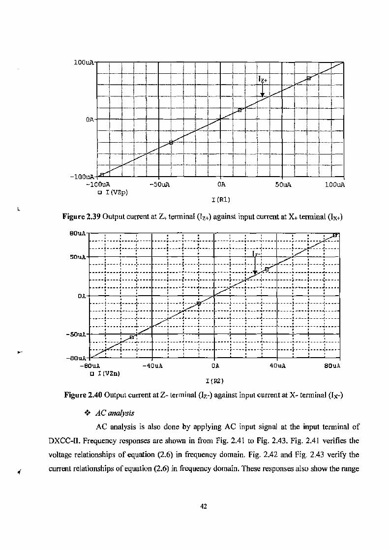
Fig. 2.57 and Fig. 2.58 show the variations in output current at terminal Z+ (lz+) and output current at terminal Z- (Iz-) with respect to the input current at X+ terminal (lx+) and input current
at X- terminal (Ix-) respectively. These responses of output currents show the linearity of the
proposed active element. Fig. 2.57 and Fig. 2.58 also verify the current relationships of equation
(2.8).
I (R1)
Figure 2.57 Output current at Z, terminal (Iz-,) against input current at X+ terminal (lx+)
0uA ..
17- .-8OuA -80uA -4OuA OA 40uA BUuA
a I (VZn) I(R2)
Figure 2.58 Output current at Z. terminal (Iz..) against input current at X- terminal (Ix-)
53
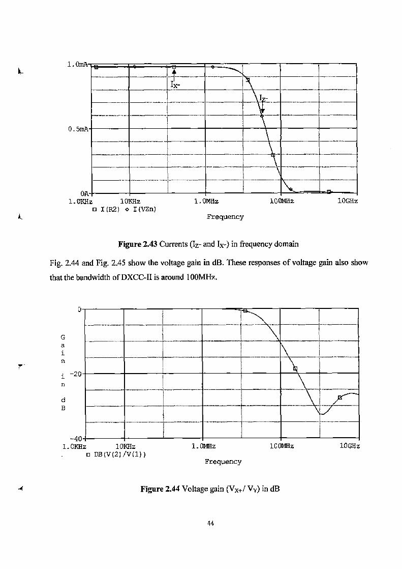
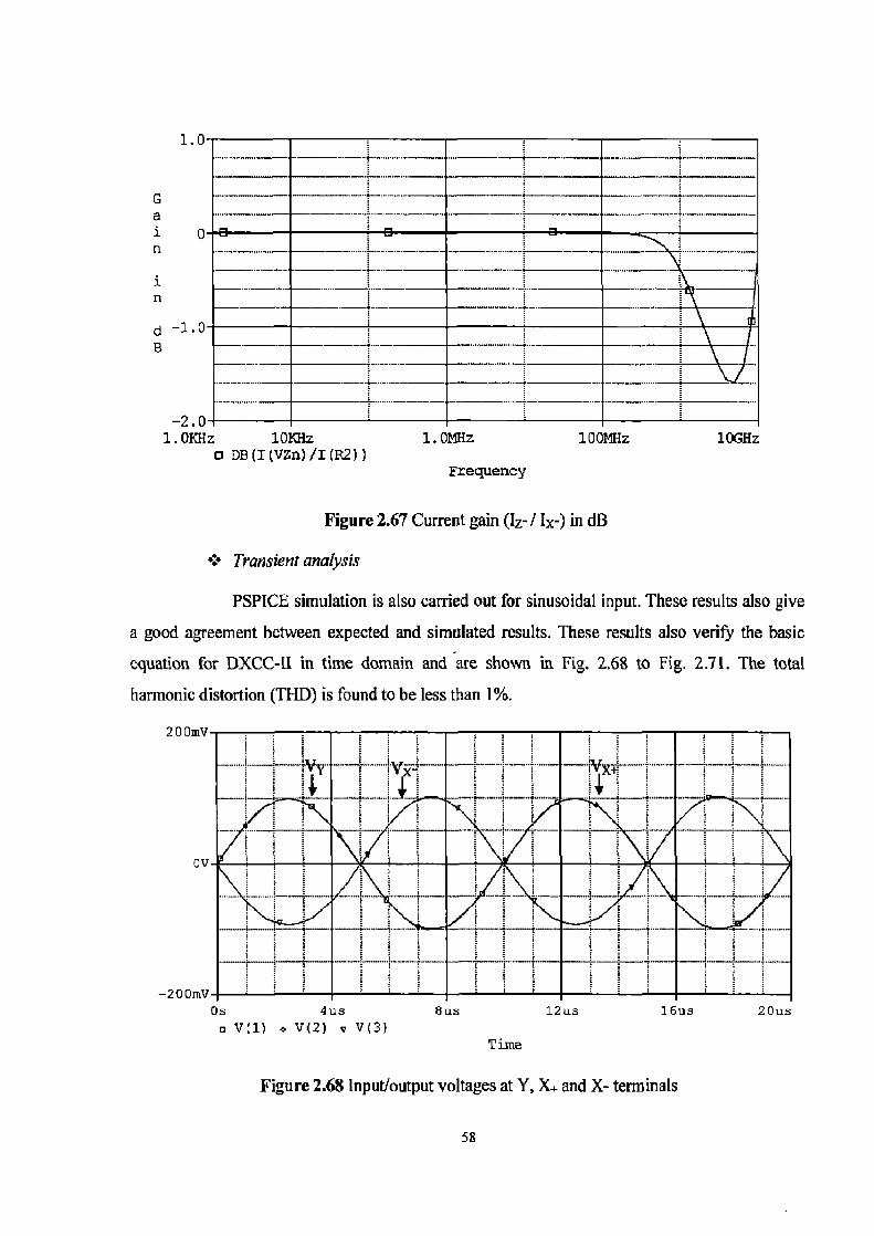
+ AC analysis
AC analysis is also done by applying AC input signal at the input terminal of
DXCC-11. Frequency responses are shown in Fig. 2.59 to Fig. 2.62. Fig. 2.59 and Fig. 2.60 verify
the voltage relationship of equation (2.8) in frequency domain. Fig. 2.61 and Fig. 2.62 verify the
current relationship of equation (2.8) in frequency domain. These responses also show the range
of frequency suitable for operation. Fig. 2.59 to Fig. 2.62 clearly indicates that voltages and
currents relationship is accurate up to 50M1-Iz. 1.ov
PSPICE simulation is also carried out for sinusoidal input. These results also give
a good agreement between expected and simulated results. These results also verify the basic
equation for DXCC-II in time domain and are shown in Fig. 2.68 to Fig. 2.71. The total
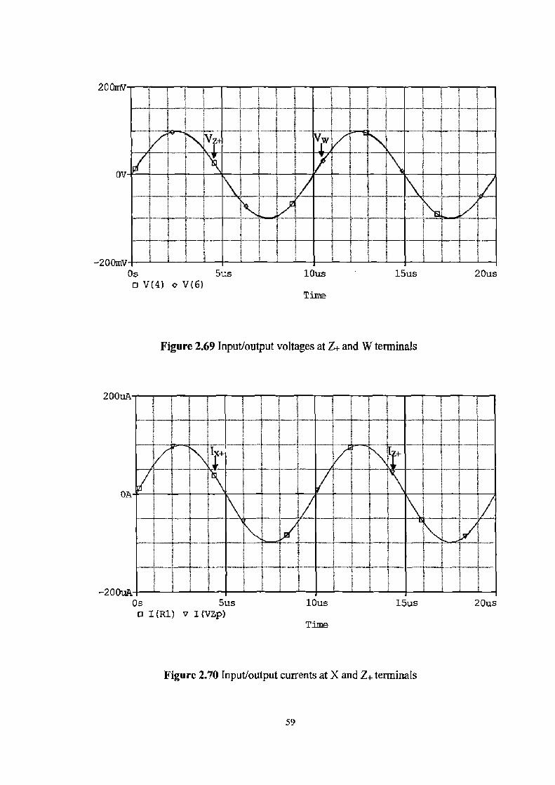
harmonic distortion (THD) is found to be less than 1%.
T ime
Figure 2.68 Input/output voltages at Y, X and X- terminals
58
7I± 1IVTIIII11 ....
5us 15us 20us o V(6)
20 OmV
Ov.
—200ntV 05 o V(4)
-200uA- - - 0$ ci I(R1)
2 OOuA
OA
II I.iI J2
Sus IOUs V I (VZp)
Time
l5us 20us
Tirm
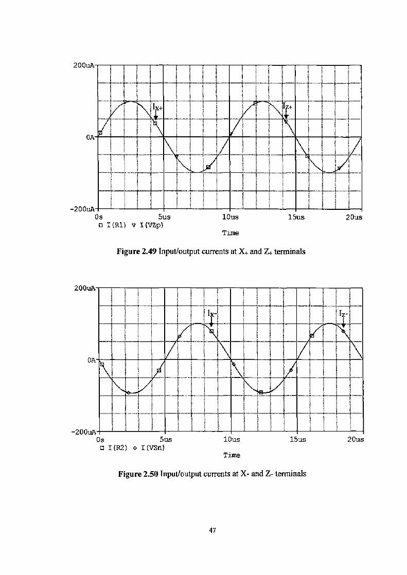
Figure 2.69 Input/output voltages at L- and W terminals
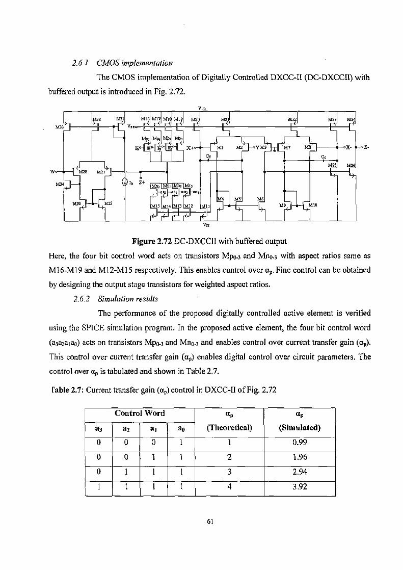
Figure 2.70 Input/output currents at X and Z+ terminals
59
! - 3
~ # t
_ S
t i
~ - ? E i
5us IOus Z5us 20us o I(VZn)
Time
200uA-
-200uA Os ❑ I (R2)
Figure 2.71 Input/output currents at X and Z- terminals
2.6 Proposed digitally controlled active elcmentt
Interesting improvements to the circuit proposals presented in the next chapters are
possible through some design modifications. A conventional DXCC-II is ideally characterized by
unity voltage as well as current transfer gains (please refer to equation (2.8)). Recently some
innovative enhancements to DXCC-lI were proposed [17]. One of these enhancements has
already been employed in this chapter in the form of DXCC-II with buffered output. Another
design modification presented in [17] was the gain variable DXCC-II, where the voltage transfer
gain was made variable in the AD-844 based realizations. Parallel to this enhancement will be
another gain variable DXCC-II with variable current transfer gain (referred to ap and a„). As the
performance parameters of most of the applications depend on current transfer gains. Therefore
if the active building block is replaced by a current gain variable DXCC-II, then further
flexibility of controlling the performance parameters can be achieved. Such enhancements will
enable possible digital control over circuit parameters by way of employing appropriate
techniques [18, 19]. Significant circuit improvement and automation can therefore be achieved
by designing current conveyors with non unity and variable transfer gains.
t The content is based on the author communicated paper P,1.
60
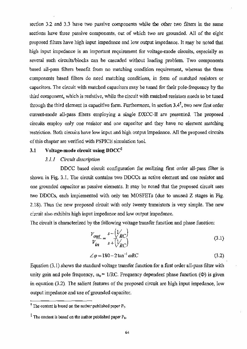
2.6.1 CMOS implementation
The CMOS implementation of Digitally Controlled DXCC-II (DC-DXCCII) with
buffered output is introduced in Fig. 2.72.
us:
Figure 2.72 DC-DXCCII with buffered output
Here, the four bit control word acts on transistors MpQ_3 and Mn4_3 with aspect ratios same as
M I 6-M 19 and Ml 2-M 15 respectively. This enables control over ap. Fine control can be obtained
by designing the output stage transistors for weighted aspect ratios.
2.6.2 Simulation results
The performance of the proposed digitally controlled active element is verified
using the SPICE simulation program. In the proposed active element, the four bit control word
(a3a2alao) acts on transistors Mp0_3 and Mn0_3 and enables control over current transfer gain (ap).
This control over current transfer gain (ap) enables digital control over circuit parameters. The
control over ap is tabulated and shown in Table 2.7.
Fable 2.7: Current transfer gain (av) control in DXCC-II of Fig. 2.72
Control Word
(Theoretical)
ap
(Simulated) a3 a2 aI -ao
0 0 0 1 1 0.99
0 0 1 1 2 1.96
0 1 1 1 3 2.94
1 1 1 1 4 3.92
61
2.7 Concluding remarks
In this chapter, an overview of DVCC, DDCC, VC-DDCC and DXCC-II along with their
CMOS implementation is presented. Furthermore, DXCC-II with buffered output and DC-
DXCCII with buffered output are proposed. The CMOS implementations of both active elements
are also given.
The important characteristics with non-ideal equations, parasitic study and simulation
results of all active elements are given. Device enhancements are further discussed as future
solutions along with some results on digital control over current transfer gain of the active
element.
62
CHAPTER 3
PROPOSED FIRST ORDER ALL-PASS SECTIONS
All-pass filters are used to correct the phase shifts caused by analog filtering operations
without changing the amplitude of the applied signal. In the literature, many first order all-
pass filters were proposed using different types of current conveyors such as [20-54]. Most of
the papers are on first order voltage-mode (VM) all-pass filter [20-47 and 49-54]. Although
the recently proposed DVCC based VM all-pass filters in [43-44] employ grounded
capacitors and resistors, which are advantageous in the reduction of parasitic impedance
effects as well as in easy integration in VLSI systems, they still suffer from the need of
passive component matching. In one work, a resistor less VM all-pass filter employing two
DVCCs and a single grounded capacitor has also been reported [15]. Although the proposed
circuit in [44] does not require a matching condition and provides low output impedance, it
still suffers from a lack of high input impedance. The most recent circuits of first order
voltage-mode all-pass filter [47] use a single active element as FDCC-II and two grounded
passive components. The circuits also enjoy the feature of high input impedance and low
output impedance. But the FDCC-II based work [47] employs as many as 35 transistors along
with a floating current source, which is cumbersome to implement. The DDCC based all-pass
filters in [29, 31] offer good options. However, all of these filters do not possess high input
impedance and/or low output impedance. The work [29] presented an all-pass filter using
differential difference current conveyor (DDCC). Similar to [29], recently presented an all-
pass filter using DDCC with minimum number of passive elements [31].
In this chapter, different circuits of first order voltage-mode all-pass filter are given.
In section 3.1', a new circuit of first order all-pass filter, using only two DDCCs, one resistor
and one grounded capacitor is proposed. The proposed filter does not need any matching
condition to realize the ail-pass filter transfer function and enjoys both high input and low
output impedance features. The non-ideal analysis of the proposed filter is also given. In
addition, the parasitic impedance effects of the active elements on the proposed filter are
investigated. Next, section 3.2' and 3.3* presents eight new first order voltage-mode all-pass
filters. All the circuits employ single DXCC-II with buffered output. The first two filters in
The content is based on the author published papers P8. P1 . 63
aeetion 3.2 and 3.3 have two passive components while the other two filters in the same
sections have three passive components, out of which two are grounded. All of the eight
proposed filters have high input impedance and low output impedance. It may be noted that
high input impedance is an important requirement for voltage-mode circuits, especially as
several such circuits/blocks can be cascaded without loading problem. Two components
based all-pass filters benefit from no matching condition requirement, whereas the three
components based filters do need matching conditions, in form of matched resistors or
capacitors. The circuit with matched capacitors may be tuned for their pole-frequency by the
third component, which is resistive, while the circuit with matched resistors needs to be tuned
through the third element in capacitive form. Furthermore, in section 3.41, two new first order
current-mode all-pass filters employing a single DXCC-II are presented. The proposed
circuits employ only one resistor and one capacitor and they have no element matching
restriction. Both circuits have low input and high output impedance. All the proposed circuits
of this chapter are verified with PSPICE simulation tool.
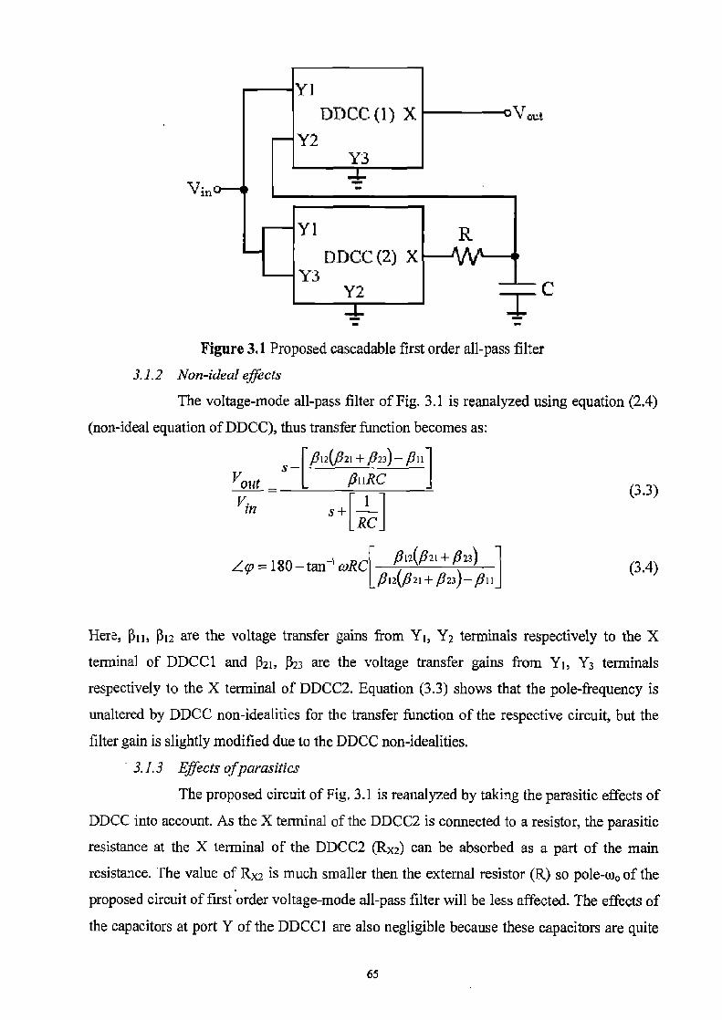
3.1 Voltage-mode circuit using DDCCt
3.1.1 Circuit description
DDCC based circuit configuration for realizing first order all-pass filter is
shown in Fig. 3.1. The circuit contains two DDCCs as active element and one resistor and
one grounded capacitor as passive elements. It may be noted that the proposed circuit uses
two DDCCs, each implemented with only ten MOSFETs (due to unused Z stages in Fig.
2.18). Thus the new proposed circuit with only twenty transistors is very simple. The new
circuit also exhibits high input impedance and low output impedance.
The circuit is characterized by the following voltage transfer function and phase function:
1 Vout (3.1) ~n s+ VRC
/gyp =1$0-2 tan coRC (3.2)
Equation (3.1) shows the standard voltage transfer function for a first order all-pass filter with
unity gain and pole frequency, coo = 1/RC. Frequency dependent phase function (t) is given
in equation (3.2). The salient features of the proposed circuit are high input impedance, low
output impedance and use of grounded capacitor.
t The content is based on the author published paper P7.
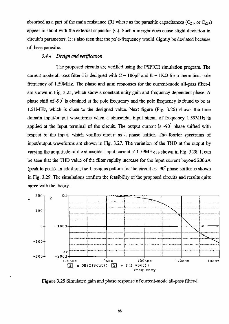
t The content is based on the author published paper P.
64
Yl DDCC(l)XI v"'t
Y2 Y3
YE I R DDCC(2) X
Y3 y2 T C
.a. Figure 3.1 Proposed cascadable first order all-pass filter
3.1.2 Non-ideal effects
The voltage-mode all-pass filter of Fig. 3.1 is reanalyzed using equation (2.4)
(non-ideal equation of DDCC), thus transfer function becomes as:
s_ fi12 21+f23) fill
____ LVout = /6uRC (3.3)
Vi IRC
Zip =180—tan coRC fi''-(fi21+#23) 1 (3.4) Ij612(1021 + fl23)— f 11
Here, P11, X312 are the voltage transfer gains from Y1, Y2 terminals respectively to the X terminal of DDCC1 and (32L, P23 are the voltage transfer gains from Yi, Y3 terminals respectively to the X terminal of DDCC2. Equation (3.3) shows that the pole-frequency is
unaltered by DDCC non-idealities for the transfer function of the respective circuit, but the
filter gain is slightly modified due to the DDCC non-idealities.
3.1.3 Effects ofparasitics
The proposed circuit of Fig. 3.1 is reanalyzed by taking the parasitic effects of
DDCC into account. As the X terminal of the DDCC2 is connected to a resistor, the parasitic resistance at the X terminal of the DDCC2 (Rx2) can be absorbed as a part of the main
resistance. The value of Rx is much smaller then the external resistor (R) so pole-w0 of the proposed circuit of first order voltage-mode all-pass filter will be less affected. The effects of
the capacitors at port Y of the DDCC1 are also negligible because these capacitors are quite
65
small (and process dependent) as compared to the external capacitors. However, the effective
value of the resistor and capacitor after parasitic inclusion is given below:
R' = R+R and C' = C+Cy12 (3.5)
where, Rxz is the parasitic resistance at X terminal of the DDCC2 and Cv12 is the
parasitic capacitor of Y2 terminal of DDCC 1.
From equation (3.5) it is clear that the parasitic resistor of X terminal of the DDCC2 appears
in series with the external resistor (R) and parasitic capacitor of Y2 terminal of DDCCI
appears in shunt with external capacitor (C). So the transfer function of the proposed first
order all-pass filter circuit including parasitic effects is given as:
RY12 — R'
'out Rr12R'C'
Tf~n RY12 + R' (3.6) s+
Rr12R'C'
where R' = R+R , C' = C+Cy12 and Ry12 is the parasitic resistor of Y2 terminal of DDCC 1.
Equation (3.6) suggests that pole and zero frequency would be different. However, for typical
design (R' << RY12), the modified pole and zero frequencies are to be in close proximity so as
to justify all-pass operation. Therefore, it is to be concluded that the circuit is not adversely
affected by the parasitic capacitances and X terminal resistance.
3.1.4 Simulation results
The voltage-mode all-pass filter of Fig. 3.1 was simulated using the CMOS
implementation of DDCC. The circuit of voltage-mode all-pass filter was designed with
C=10pf, R=10KQ. The designed pole-frequency is 1.59MHz. The simulation results show a
pole frequency of 1.57MHz that closely matches the designed frequency. The discrepancy in
the pole frequency is due to the non idealities as discussed in the previous sub-sections. The
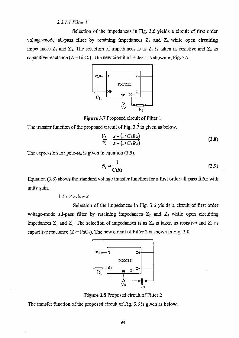
gain plot of the circuit of Fig. 3.1 is shown in Fig. 3.2, while phase plot is shown in Fig. 3.3.
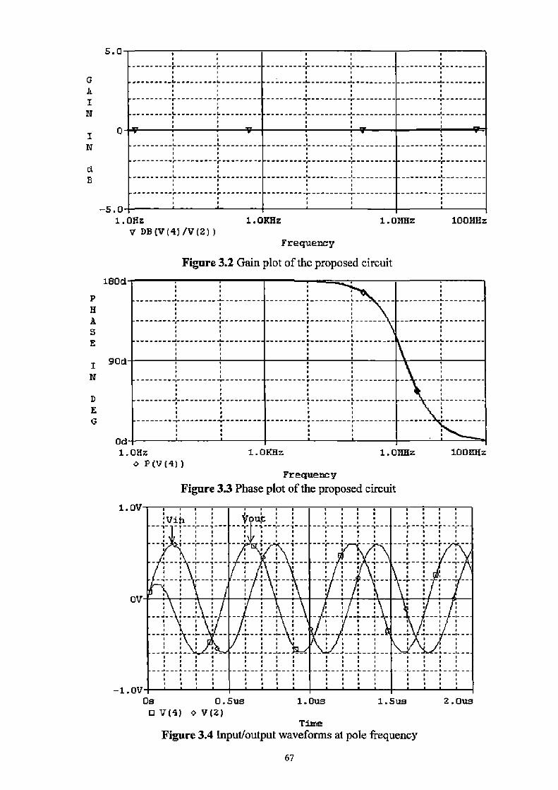
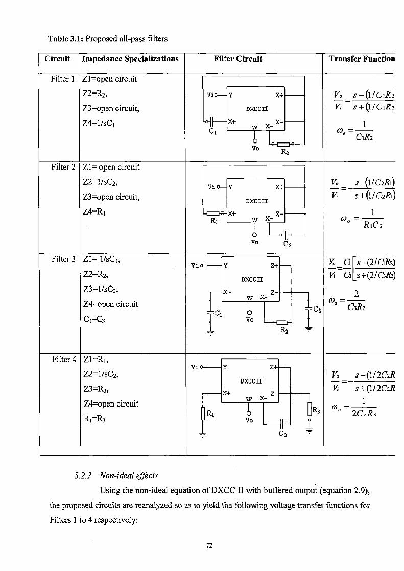
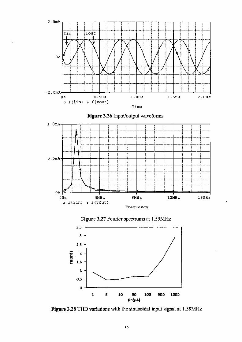
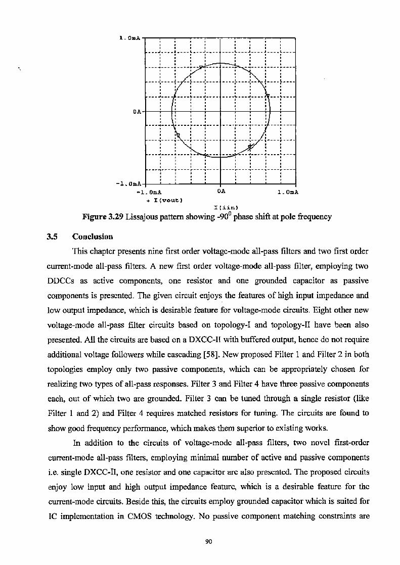
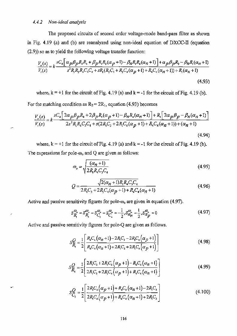
Next, Fig. 3.4 shows that at the pole frequency of 1.59MHz input/output waveforms are 900
phase shifted as expected. The Fourier spectrum of the output is shown in Fig. 3.5. The total
harmonic distortion (THD) of the proposed circuit is within 2%.
66
5.0-
G A
Y N
0.
N
d B
I 1 1 i . I I 1 , I 1 I --------r---------r--------- ---- ----r------_--,---------- ------- -r -------- 1 1 1 1 1 I I . r
.r-----1-------- 1--aa. af~ ► a ar.-r.J-..-r. r- rr-rr-rrL-.r...rJr.rrrrr~J--......L
------ 1 - 1 1 I 7 1 1 1 I I I 1 I 1 1 i 1 I A
5Ons 1DOns
D .
-2 00niV Os n ;1(11 o V(5)
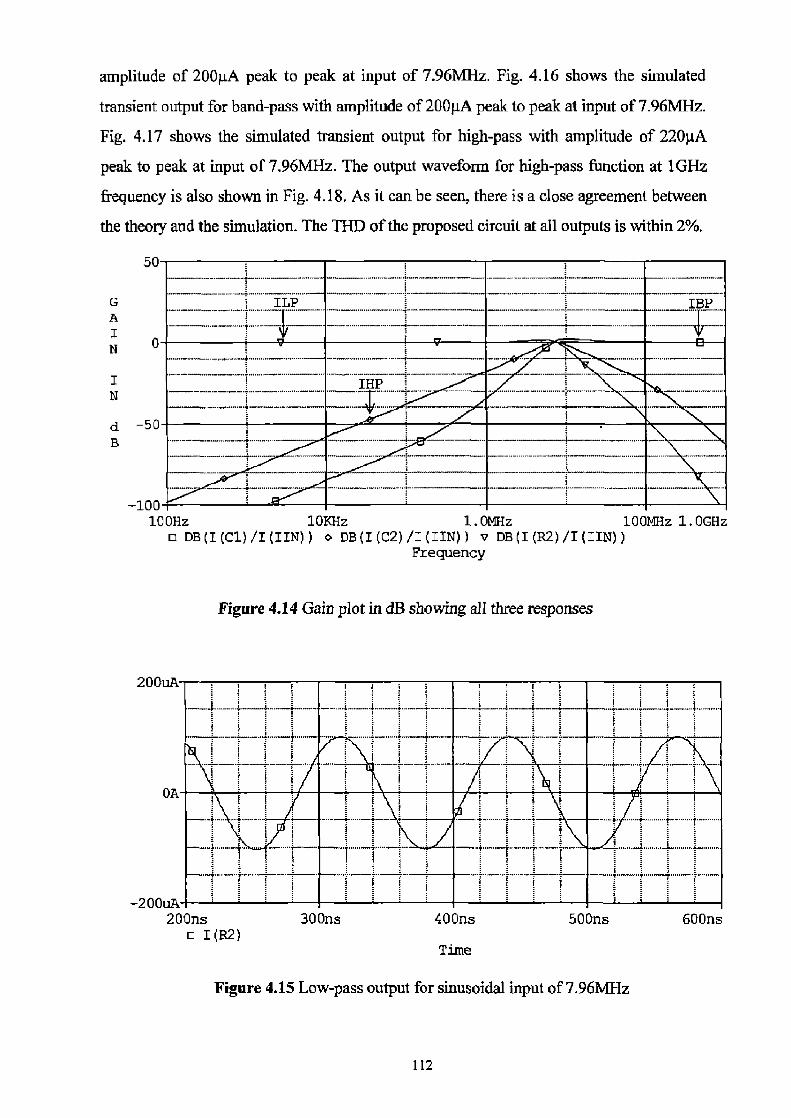
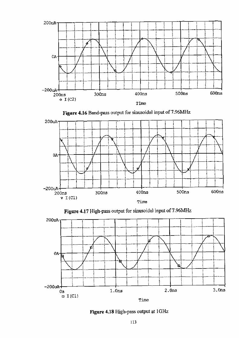
used is of 5KS~ and capacitor used is of value 1.27pF. The frequency response of Filter 1 is
shown in Fig. 3.11, which shows that the pole frequency is 24.93MHz with a percentage error
of 0.28%. The usefulness of new circuits is to be especially emphasized keeping in view the
design frequency which is quite high. The input/output waveforms are shown in Fig. 3.12.
The time-domain output at the pole frequency was found to show THD of as small as
0.79%, which is a very low value keeping in view the operating frequency. Next, the signal
amplitude was varied from lmV to 500mV and the ThD curve plotted. It is seen from Fig. 3.12 that the TFID is within 1% for nearly two decade variation in input signal amplitude. Fig. 3.12 shows a very good dynamic range of the new circuit topology.
20 c A 0 I
_20
- 4C 0 DB(V(5)/V(1) )
1504 P H 100d A
50d E SEL~~
Od 1.0Hz 100Hz 10F~iz
0 P(V(5)) Frequency
1.4HHz 10 01Hz
Figure 3.11 Frequency response of Filter 1
Time
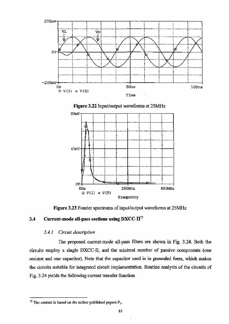
Figure 3.12 Input/output waveforms at 25MHz
75
7
6
0 100 2O0 300 400 sco 600
lnputVoltage (mV)
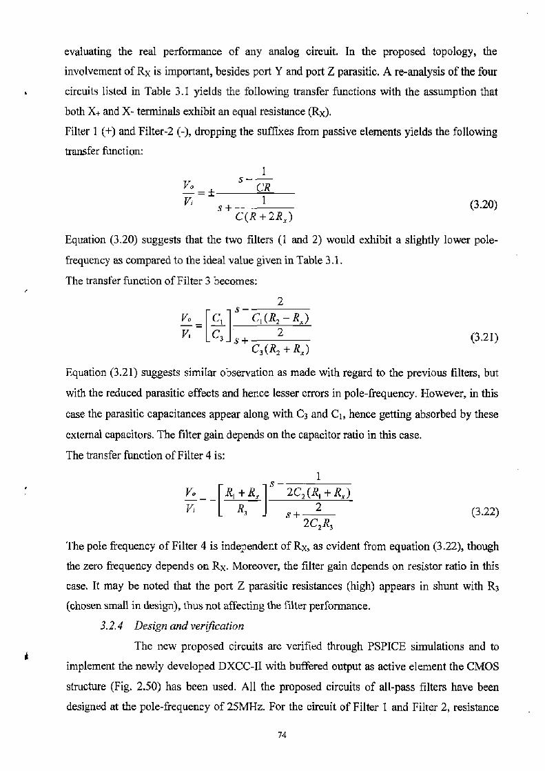
Figure 3.13 THD variations at output with signal amplitude at 25MHz
3.2.E Experimental realization using AD-844
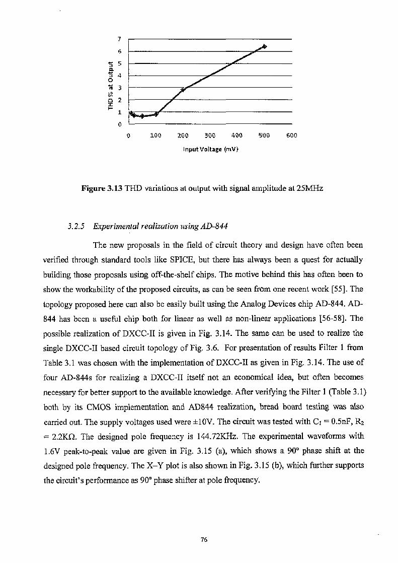
The new proposals in the field of circuit theory and design have often been
verified through standard tools like SPICE, but there has always been a quest for actually
building those proposals using off-the-shelf chips. The motive behind this has often been to
show the workability of the proposed circuits, as can be seen from one recent work [55]. The
topology proposed here can also be easily built using the Analog Devices chip AD-844. AD-
844 has been a useful chip both for linear as well as non-linear applications 156-58]. The
possible realization of DXCC-II is given in Fig. 3.14. The same can be used to realize the
single DXCC-II based circuit topology of Fig. 3.6. For presentation of results Filter 1 from
Table 3.1 was chosen with the implementation of DXCC-II as given in Fig. 3.14. The use of
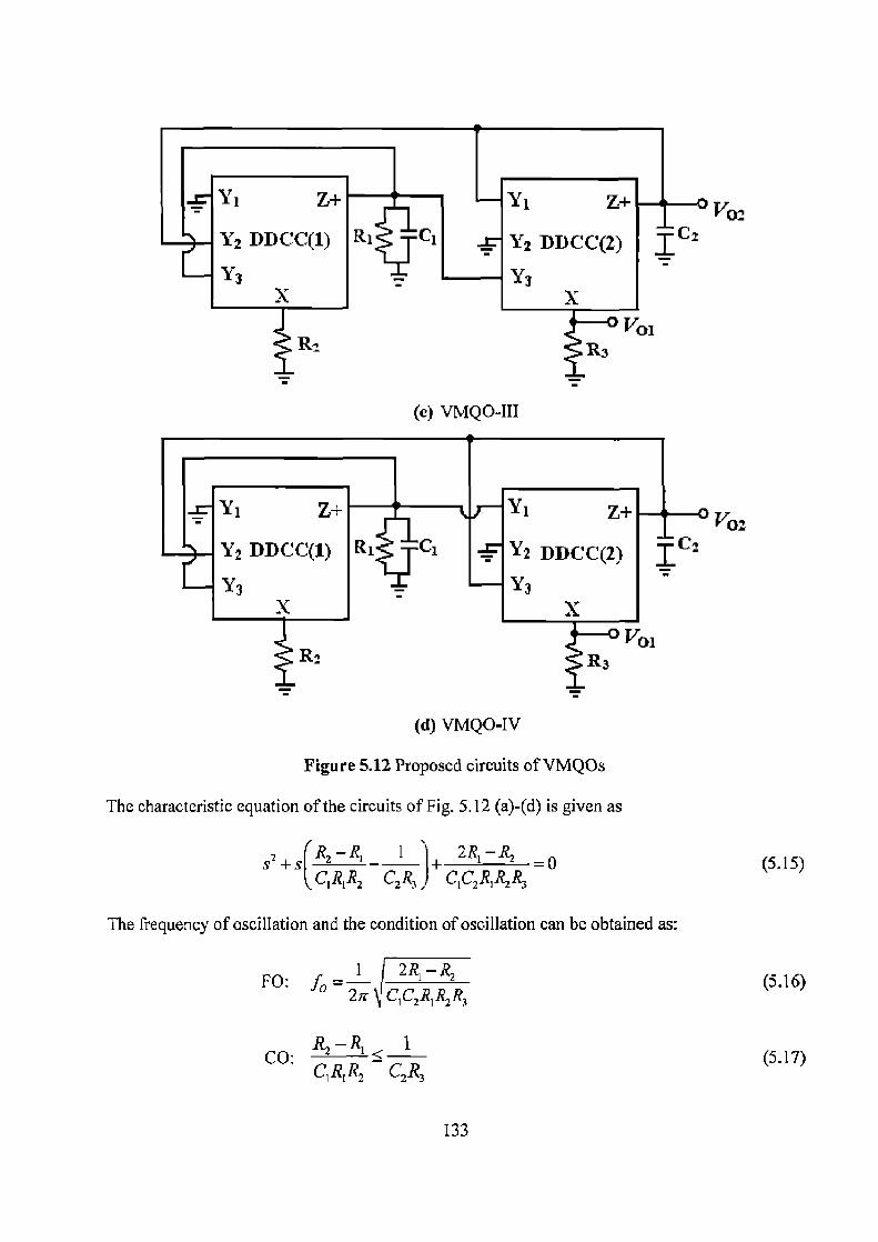
four AD-844s for realizing a DXCC-II itself not an economical idea, but often becomes
necessary for better support to the available knowledge. After verifying the Filter 1 (Table 3.1)
both by its CMOS implementation and AD844 realization, bread board testing was also
carried out. The supply voltages used were ±1OV. The circuit was tested with Ct = 0,5nF, R2
2.2KO. The designed pole frequency is 144.72KHz. The experimental waveforms with
1.6V peak-to-peak value are given in Fig. 3.15 (a), which shows a 900 phase shift at the
designed pole frequency. The X—Y plot is also shown in Fig. 3.15 (b), which further supports
the circuit's performance as 900 phase shifter at pole frequency.
76
Y
z+'
13T
Figure 3.14 Possible experimental realization of DXCC-II using AD-844s
3 WI DU L TRACE aSCJLtOS[OP£ Lu
(a)
(b)
Figure 3.15 (a) Experimentally obtained input/output waveforms (1.6 V peak-to-peak,
3.3 Voltage-mode circuits using port interchange in DXCC-Xl**
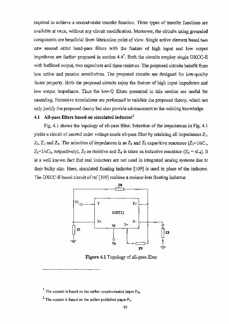
The new additional topology for voltage-mode first order all-pass filter is obtained by
interchanging the positions of X+ and X- in Topology-I (Fig. 3.6) of previous section.
3.3.1 Topology-ll
The new additional topology for first order voltage-mode all-pass filter is
shown in Fig. 3.16. Z4
Z2
Figure 3.16 Topology extension by interchanging X .ports
The given topology is characterized by the general transfer function as below:
Vd — Z2Z3Z4 + 2Z1Z2Z3 — 2Z1Z3Z4 (3.23)
V, ^ Z]Z2Z4 +2Z,Z2Z3 +2Z1Z3Z4
Specialization of the impedances in Fig. 3.16 yields four new circuits of first order all-pass
filter as described below.
3.3.1.1 Filter 1
Selection of the impedances in Fig. 3.16 yields a circuit of first order
voltage-mode all-pass filter. In the circuit of Filter 1, Z2 and Z4 are retained with Z2 as a
resistor and Z4 as a capacitor, while open-circuiting Z1 and Z3. No matching condition is
required. The new circuit of Filter I is shown in Fig. 3.17.
ri Y Z+
DXCCII
- w X+-
1
Vo R1
Figure 3.17 Filter 1
" The content is based on the author published papers P5.
78
The transfer function of the proposed circuit of Fig. 3.17 is given as below.
Vo s—(11C1R2) (3.24)
Vi r s + {1I C1R2)
The expression for pole-tea is given in equation (3.25).
_ 1
~° CiR (3.25)
Equation (3.25) shows the standard voltage transfer function for a first order all-pass filter
with unity gain.
3.3.1.2 Filter 2
Selection of the impedances in Fig. 3.16 yields a circuit of first order
voltage-mode all-pass filter. In the circuit of Filter 2, Z2 and Z4 are retained with Z2 as a
capacitor and Z4 as a resistor, while open-circuiting Zi and Z3. No matching condition is
required. The new circuit of Filter 2 is shown in Fig. 3.18.
Figure 3.18 Filter 2
'he transfer function of the proposed circuit of Fig. 3.18 is given as below.
Vo _ s-(11C2RI) V s + (1 l C2RI)
(3.26)
Che expression for pole-o 0 is given in equation (3.27).
m o = 1 (3.27) RIC2
;quation (3.27) shows the standard voltage transfer function for a first order all-pass filter
rith unity gain.
3.3.1.3 Filter 3
Selection of the impedances in Fig. 3.16 yields a circuit of first order
-oltage-mode all-pass filter. In the circuit of Filter 3, Z1, Z2 and Z3 are retained with Z1, Z3 as
capacitor and Z2 as a resistor, while open-circuiting Z4. The new circuit of Filter 3 is shown
n Fig. 3.19.
79
Vio—IY
DXCCII
X— 2- w X+
_Lc LJ 3
To r R2
Figure 3.19 Filter 3
The transfer function of the proposed circuit of Fig. 3.19 is given as below.
Y _ Ci s—(21 CiR2) (3.28)
V C3 s+(21 C31 Z)
The expression for pole-o 0 is given in equation (3.29).
2 C3Rz
(3.29)
Equation (3.29) shows the standard voltage transfer function for a first order all-pass filter
with unity gain for matched capacitors (C1=C3).
3.3.1.4 Filter 4
Selection of the impedances in Fig. 3.16 yields a circuit of first order
voltage-mode all-pass filter. In the circuit of Filter 4, ZI , Z2 and Z3 are retained with Z1, Z3 as
a resistor and Z2 as a capacitor, while open-circuiting Z4. The new circuit of Filter 4 is shown
in Fig. 3.20.
Vi
Figure 3.20 Filter 4
The transfer function of the proposed circuit of Fig. 3.20 is given as below.
V. s-(1r2C2Ri) V —s+(1!2C2R3)
(3.30)
br The expression for pole-(oo is given in equation (3.31).
o = 1 (3.31) 2C2R3
so
Equation (3.31) shows the standard voltage transfer function for a first order all-pass filter
with unity gain for matched resistors (R,=R3).
The circuits of Filter 1 and Filter 2 use two passive components. In the last two
circuits of Filter 3 and Filter 4 three components are used in each. The circuits of Filter 1 and
Filter 2 enjoy the advantage of single resistor control. The circuit of Filter 3 also enjoys the
feature of single resistor control but is non-canonical. It also employs both capacitors in
grounded form. The circuit of Filter 4 is canonical by employing single capacitor, but
requires matched grounded resistors. All four filters are further tabulated and shown in Table
3.3. It is also to be noted that other useful first order analog functions (for instance lossy and
loss less integrators, high pass filter etc) are also realizable from the modified general
topology of Fig. 3.16.
3.3.2 Non-ideal analysis
Using the non-ideal equation of DXCC-11 with buffered output (equation 2.9),
the proposed circuits are reanalyzed. The voltage transfer functions for Filters 1 to 4 are as
follows respectively:
5— (an + 1)/n
Vo_ _ (ap + I ) C i R 2 Vi y~ p a n + 1 3.32)
[ S+ (aP + 1 >C iR z
,l3p(a, + 1 ) Vo _ s 6.0 2R1(an+ 1
n Vi Y s +
(a + 1 ( 3.33)
(an+1 C2RI
(a n + 1 )p n
Vo _ C I aPf3FC iR 2 Vi r _
Ya p fp ~- 3 a n+ 1 (3.34 )
s + C 3R 2
a p/J p ___ rVo fln(a n + 1 ~C 2R I Vi Y'i n — 1 (3.35)
s + (an + 1)C 2R 3
81
Table 3.3: Proposed all-pass filters
Circuit Impedance Specializations Filter Circuit Transfer Function
Filter 1 Z1=open circuit
Z2=R2, Vi Y Z+ V. —
$ — (1 / CiR __ Z3=open circuit, DXGCII F1 s + (1l CiR
Z4=1/sCi x_ Z_ Cl ~" 1
CiR 2 ° R a
Filter 2 Z1= open circuit
Z2=1 /sC2, V. s - (1 / C2RI) _
Z3=open circuit, Vi Y Z+
V s + (1/ C2Ri) DX cczx
Z4=R1 x_ 1
Z_ w X+ 1 R1C2
vo Cs
Filter 3 Z1= 11sC1, Vi Y Z+
Z2=R2, DXCCIz Y C~ s—(2/ CiRi Z3=1ISC3, X- ~- V
_ C3 s+(2I C3R2
Z4=open circuit CI=C3 Va [_ } c 2
0)0 = C~R2 a
Filter 4 Z1=R1 , 1i Y Z+
Z2=1lsC2, Yo s — (112C2R1) ~xccz~
Z3=R3, >_ Z _ V s+(I/2C2R3)
Z4=open circuit w X+
w = 1
R1=R3 Ri
Vo
2C 2R3
C2
.r The pole-coo sensitivity for the circuits of all pass filters to the non-idealities as well as to the
external components is analyzed and is tabulated in Table 3.4,
82
Table 3.4: Sensitivity figures
Sensitivities Filter 1 Filter 2 Filter 3 Filter 4
S ~C -1 -1 -1 -1
~o 'S&P _
(ap + 1) a r
(p+1) 0 0
SaA an an
(an + 1) an
(an + 1) all
(an + 1) (an + 1)
S0 Al
0 0 0 0
Sao Al
0 0 0 0
The sensitivity figures for the proposed circuits are all equal to or less than unity in
magnitude which implies good sensitivity performance.
3.3.3 Parasitic study
A re-analysis of the four circuits listed in Table 3.3 yields the following
transfer functions with the assumption that both X+ and X- terminals exhibit an equal
resistance (Rx).
Filter 1 (+) and Filter 2 (-), dropping the suffixes from passive elements yields:
1
V. s_
CR V~
5+ 1 (3.36) C(R+2Rx )
Equation (3.36) suggests that the two filters (1 and 2) would exhibit a slightly lower pole-
frequency as compared to the ideal value given in Table 3.3.
Filter 3 transfer function becomes:
s- 2
V. _ C1 C1(R2 —1)
V, C3 s + 2 (3.37) C'3(R2+R )
Equation (3.37) suggests similar observation as made with regard to the previous filters, but
with the reduced parasitic effects and hence lesser errors in pole-frequency. However, in this
case the parasitic capacitances appear along with C3 and C1 , hence getting absorbed by these
external capacitors. The filter gain depends on the capacitor ratio in this case.
Filter 4 transfer function is:
83
I s~
V, R, + Rx 1 2C2 (R1 + R1) Y` R3 s + 2 (3.38)
2C2R3
The pole frequency of Filter 4 is independent of Rx, as evident from equation (3.38), though
the zero frequency depends on R. Moreover, the filter gain depends on resistor ratio in this
case. It may be noted that the port Z parasitic resistances appears in shunt with R3, thus not
affecting the filter performance.
3.3.4 Simulation results
The new proposed circuits are verified through PSPICE simulations. All the
proposed circuits of all-pass filters have been designed at the pole-frequency of 25MHz. For
the circuit of Filter 1 and Filter 2 (Table 3.3), resistance used is of 5K! and capacitor used is
of value 1.27pF. The frequency response of Filter 1 is shown in Fig. 3.21, which shows that
the pole frequency is 24.46NJTIz with a percentage error of 0.16%. The input-output
waveforms are shown in Fig. 3.22. Frequency spectrum of the input/output waveform is
shown in Fig. 3.23. The time-domain output at the pole frequency was found to show THD of
as small as 0.62%.
40
Cr 20
I 0
N -20
-40 13 DB (V 5) /V (1) )
P Oct
H A
-200d E
SEL>> -400d
1.0Hz 100Hz 10KHz o P(V(5))
Frequency
1.0KHz 100I3Hz
Figure 3.21 Frequency response of Filter I
84
—200mV Os ❑ v(1) o v(5)
200mV-
OY .
Vi Vo€
50ns loons Time
Figure 3.22 Input/output waveforms at 25MHz 80mV
4 OM%
200MHz 400MHz
Frequency
Figure 3.23 Fourier spectrums of input/output waveforms at 25MHz
3.4 Current-mode all-pass sections using DXCC-IItt
3.4.1 Circuit description
The proposed current-mode all-pass filters are shown in Fig. 3.24. Both the
circuits employ a single DXCC-II, and the minimal number of passive components (one
resistor and one capacitor). Note that the capacitor used is in grounded form, which makes
the circuits suitable for integrated circuit implementation. Routine analysis of the circuits of
Fig. 3.24 yields the following current transfer function
tt The content is based on the author published papers P7.
ov 0Hz
❑ V(1) o V(5)
i -
85
I
'° — CR (3.39) ~IN 5 +
CR
The frequency dependent phase response (0) of the filters is given by
0(w) = —2 tan-1 (rvCR) (3.40)
It is to be noted from equation (3.39) that no passive element matching constraints are required for the proposed circuits. The proposed filters exhibit low input and high output impedance, which make them suitable for cascading without requiring additional current buffer circuit.
Mode of Voltage Voltage Voltage Voltage Voltage Voltage Voltage Current Operation Number of Two One One One One One One ' One
active elements
Number of One One One Two One One Two One resistors
Number of One One Two One One Two One One capacitors
Input High High High High High High High Low impedance
Output Low Low Low Low Low Low Low High impedance Designed 1.59MHz 25MHz 25MHz 25MHz 25MHz 25MHz 25MHz 1.59MHz
pole- frequency Type of DDCC DXCCII DXCCII DXCCII DXCCII DXCCII DXCCII DXCCII active
element
Furthermore, non-ideal analysis and parasitic considerations for all the circuits are
also given. Simulations results are given to verify the theory. The new developed circuits are
expected to further enhance the existing knowledge on the subject.
91
CHAPTER 4
PROPOSED SECOND ORDER FILTER CIRCUITS
It is well known that current conveyor and its different variations have received significant
attention because of their high performance attributes such as extended bandwidths and
high values of slew rates [1]. Second order active filters using different kinds of active
elements are of great interest, since several cells of that kind can be connected in cascade
to implement higher order filters. It is important to realize these active filters using a
minimum number of active and passive elements, since simplicity, cost reduction, power
consumption and versatility are all important for the integrated circuit designers. In
addition to these features, numerous circuits presented in the literature realizing second
order transfer functions exhibit different properties concerning the operation mode,
sensitivity, integrability, etc. Therefore, numerous circuits reported in the literature tend to
employ a minimum number of active and/or passive components [1, 60-74]. Current-mode
analog signal filtering has also received a lot of attention in the recent past. Thus, several
multifunction or universal hi-quadratic filters using current conveyors have been reported
in the literature [13, 75-106]. It may be noted that analog filters continue to appear in open
literature as a potential analog block for larger subsystems [21, 27, 28, 46, 47, 49, 107,
108].
This chapter presents second order filter circuits. Second order all-pass filters with
the features of high input and low output impedance are presented in first two sections. In
section 4.1#, floating simulators have been employed to overcome the drawbacks of
passive inductors [109]. It may be noted that floating inductor simulators using current
conveyors have been researched well in literature [12, 110-112]. Transformation technique
has further been employed in section 4.2* to realize simpler alternative with lesser circuit
complexity. Section 43* presents a new second order current-mode biquad filter circuit
employing grounded components. The circuit uses a minimum number of components
The content is based on the author published papers Ps. P4.
92
required to achieve a second-order transfer function. Three types of transfer functions are
available at once, without any circuit modification. Moreover, the circuits using grounded
components are beneficial from fabrication point of view. Single active element based two
new second order band-pass filters with the feature of high input and low output
impedance are further proposed in section 4.41. Both the circuits employ single DXCC-i1
with buffered output, two capacitors and three resistors. The proposed circuits benefit from
low active and passive sensitivities. The proposed circuits are designed for low-quality
factor property. Both the proposed circuits enjoy the feature of high input impedance and
low output impedance. Thus the low-Q filters presented in this section are useful for
cascading. Extensive simulations are performed to validate the proposed theory, which not
only justify the proposed theory but also provide advancement to the existing knowledge.
4.1 All-pass filters based on simulated inductort
Fig. 4.1 shows the topology of all-pass filter. Selection of the impedances in Fig. 4.1
yields a circuit of second order voltage-mode all-pass filter by retaining all impedances Z1,
Z2, Z3 and Z4. The selection of impedances is as ZI and Z3 capacitive reactance (Zi=1/sC1,
Z3=1fsC3, respectively), Z2 as resistive and Z4 is taken as inductive reactance (Z4 = sL4). It
is a well known fact that real inductors are not used in integrated analog systems due to
their bulky size. Here, simulated floating inductor [109] is used in place of the inductor.
The DXCC-Il based circuit of ref [109] realizes a resistor-less floating inductor. Z4
Figure 4.1 Topology of all-pass filter
t The content is based on the author communicated paper P10 .
: The content is based on the author published paper P.
93
4.1.1 Circuit-I
4.1.1.1 Circuit analysis
The new proposed second order voltage-mode all-pass filter using
simulated inductance (L4=LS;m) is shown in Fig. 4.2. The transfer function of the proposed
circuit of Fig. 4.2 is given as below.
V0 (s) _ s2LCtiR2 —2sL +2R2 (4.1)
V (S) s2Lsi,C3R2 +2sL5trr, + 2R2
The expressions for pole-u)0 and Q are given in equation (4.2) and (4.3) respectively.
cla = 2 (4.2) C3 Lsim
FC3Rz (4.3)
From equations (4.2) and (43), it is found that the Q can be tuned independent of coo by
adjusting the value of R2. Sensitivity figures for pole-u)0 and Q are given as follows:
So° =SO'° _-1,SW° =0 (4.4) C3 L.,ins 2 Rz
1,
= Q Q = I (4.5) S S = — S — 2 C3 Lsirlr 2
From the equations (4.4) and (4.5), the sensitivity figures for the proposed circuit are found
to be less than or equal to unity in magnitude which implies good sensitivity performance.
L
C3
Figure 4.2 Proposed second order all-pass filter using simulated inductor
It is now to be emphasized that inductance simulator value is as Ls jm = (C/gmlgm2), where,
gm, & gm2 are transconductance of transistors used in simulated inductor, which can be
94
controlled by the gate voltages of those transistors [109]. Here, g,; (i=1, 2) is the
transconductance of the ith MOS transistor and is given as:
gmi = 2 ppCox (VGi - VTI ) where, i 1,2 (4.6) t
By substituting the value of LS;,,, in equation (4.1), the transfer function becomes
V0 (s) _ s2CC1R2 -2sC+2R2g, 1 gm2 (4.7)
Vs (s) - S2CC3R2 +2sC+2R2gm1gm2
The expressions for pole-m and Q are also modified and given in equation (4.8) and (4.9)
respectively.
=F~3
ga (4.8)
Q = !~D C3gmlgm l2 (4 9) G z 2C
7
Sensitivity figures for pole-o0 and Q are now given as follows:
SOry'° = -S = -S = I ,S0]~'° ; 0 (4.10) 8ml1 gyn2 C3 C 2 2
SQ =l, 8Q = Sg t gm~ =_8Q=_ (4.1)
All the sensitivity figures given in equations (4.10) and (4.11) are still less than or equal to
unity in magnitude, which suggests good sensitivity performance.
4.1.1.2 Non-ideal analysis
Using the non-ideal equation of DXCC-II with buffered output (equation
(2.9)), the proposed circuit of second order voltage-mode all-pass filter using simulated
inductor as shown in Fig. 4.2 is reanalyzed so as to yield the following voltage transfer
function:
V0 (s) s2apQpLs~mC1R2 -sLsrra/3n (1+ an )+R2lp(I+ap ) (4.12) V; (s) S2L5,,,,C3R2 +sLs,m(I+an )+R2 (l+ap )
The expressions for pole-cap and Q are given as follows:
JC3L,
I+ap rip =
(4.13)
R2 C3(l+ap )
Q l + an ~ (4.14)
95
Active and passive sensitivity figures for pole-o9 and Q are given in equations (4.15) and
(4.16).
Sty° =S ev° —_-1,s'°' =0,Sa° = p ,S ° =0 (4.15) 2 Rz P 2(l+ap )
a S =1,SQ --S~lr
— 2' Sa — 2(1+aF )'Sa I+an (4.16)
The sensitivity figures are all less than or equal to unity in magnitude which implies good
sensitivity performance. Sensitivity of filter parameters to current transfer gains will also
remain less than unity for the ideal value of current transfer gains which is equal to unity.
4.1.1.3 Parasitic considerations
A study is next carried out on the effects of various parasitic of the DXCC-II
used in the proposed circuit. The proposed circuit is re-analyzed by taking into account the
parasitic effects. A re-analysis of the proposed circuit of voltage-mode second order all-
pass filter using simulated inductor as shown in Fig. 4.2 yields: P
V° (s) s2 LS1nzC1 R2 — 2sLs,.n, +2R2 , , (4.13)
V, (s) s2L5,»rC3 R Z + 2sL,ln, +2R2
where, R2' = R2+RX.. and C1' = C i+ Cx+ and C3' (C3+Cz++Cz-)
Equation (4.17) shows that the parasitic resistances/capacitances merge with the external
value. Such a merger does cause slight deviation in circuit's parameters. It can be further
observed from equation (4.17) that the order of transfer function of second order all-pass
filter is not changed. The modified expressions for pole-ce, and Q with parasitic effects are
also given in equation (4.18) and (4.19).
coo =
F~3~km
(4.18)
FC3
Q = R2 (4.19)
Next, it is seen from equation (4.18) that the pole-frequency would slightly be deviated (in
deficit) because of these parasitic. The expression showing the effects of parasitic on po1e-
Q is also given in equation (4.19). The pole-Q would also deviate slightly because of the
parasitic.
96
4.1.2 Circuit-II
4.1.2.1 Circuit analysis
Another second order voltage-mode all-pass filter using simulated
inductance (L4°Ls;m) is shown in Fig. 4.3. The circuit is obtained by interchanging the positions of the X+ and X- terminals in Fig. 4.2 and is shown in Fig. 4.3. The transfer
function of the proposed circuit of Fig. 4.3 is given as below.
V(s) ~_s2L,-;,,,C,R2 —2sLs1m + 2R2 (4.20)
V1 (s) s 2Ls1,,,C;R2 + 2sL51R, + 2R2•
The expressions for pole-a 0 and Q are given in equation (4.21) and (4.22) respectively.
coo = 2'
(4.21) C3 ~sim
FC3 ,.,Q=RZ (4.22)
From equations (4.21) and (4.22), it is found that the Q can be tuned independent of ca. by
adjusting the value of R2.
Sensitivity figures for pole-%, and Q are given as follows:
=Sw° =—I,S~° =0 (4.23)
SQ =1,SQ = —S~;n, = 2 (4.24)
From the equations (4.23) and (4.24), the sensitivity figures for the proposed circuit are
found to be less than or equal to unity in magnitude which implies good sensitivity
performance.
L. r — --~
Cs
Figure 4.3 Second-order all-pass filter using simulated inductor obtained by interchanging
X ports in Fig. 4.2
M
By substituting the value of Ls;m in equation (4.20), the transfer function becomes
V. (s) - _ s2 CC,R2 - 2sC + 2R2gr1,1gr,,2 (4.25) f (s) s2CC3R2 + 2sC +
The expressions for pole-%, and Q are also modified and given in equation (4.26) and
(4.27) respectively.
__ 2gn)XM2 (4.26) U C3C
Q = R2 r3g;:~9-~:2 (4.27)
Sensitivity figures for pole-t)o and Q are given as follows:
From equations (4.98) to (4.103), it can be further observed that the sensitivity figures for
pole-o 0 and pole-Q are all within unity in magnitude for equal resistor and capacitor
design which implies good sensitivity performance.
4.4.3 Parasitic considerations
A study is next carried out on the effects of various parasitic of the DXCC-II used
in the proposed circuits. It assumes special significance for evaluating the real performance
of any analog circuit. The various parasitic of DXCC-lII are port Z parasitic in the form of
RZI/Cz, port Y parasitic in the form of Ry//Cv and port X parasitic. The proposed circuits
are re-analyzed by taking into account the above parasitic effects. A re-analysis of the
proposed circuits of second order voltage-mode band-pass filters as shown in Fig.
8.1yields:
V(S) —k sC4R'C'(RzR4 +2R;R-2RRR4)+R'C'(RI -2R1) V,(s) s`R'RR4 C3 C4 RZ+ R _CZ+ C _ +sR1'[RC3 RZ+ RZ _CZ+Z C - +RC4 R'C'(2+R4 ) +2R4 C4 R'C']+R'C'(2+R r I Z Z
(4.104)
where, R' i = R1+Rx+, R'2 = R2+Rx-, R' = RZ++RZ_ and C' = Cz+CZ + C2.C3+ CZ+C3
From equation (4.104), it is to be observed that most of the parasitic capacitances get
absorbed with the external grounded capacitor, as are in shunt with it. Also the parasitic
resistances get absorbed with the external resistors, as it is in series with it. Such a merger
will cause a slight deviation in circuit parameters.
4.4.4 Simulation results
The proposed circuit of second order voltage-mode band-pass filter (Fig. 4.19
a) is designed with pole frequency of 15.92MHz: Ci = C2 = IOpF, R1= RA = IKQ and R2 =
2KS2. The simulated pole frequency is same as designed one. The gain response of the
117
circuit of Fig. 4.19 (a) is shown in Fig. 4.20, which shows that the pole frequency is
15.89MHz with a percentage error of 0.18%. This gain response shows that it is suitable
for narrow band applications. The usefulness of new circuits is to be especially
emphasized keeping in view the design frequency which is quite high. The input/output
waveforms for second order voltage-mode band-pass filter are shown in Fig. 4.21. The
Fourier spectrum of output is shown in Fig. 4.22. The THD is found to be 1.5%.
The Monte Carlo analysis of the second order voltage-mode band-pass filter (Fig.
4.19 a) is next performed taking 5% Gaussian deviation in the each passive component
(C1, C2, R I, R2, and R4). The analysis is done for 5 runs. The gain response with Monte
Carlo analysis is shown in Fig. 4.23 and time domain result for Monte Carlo analysis is
shown in Fig. 4.24. As depicted from Monte-Carlo analysis results, the proposed filters
have good sensitivity performances.
Next, the proposed circuit of second order voltage-mode band-pass filter (Fig. 4.19 a)
is further designed for wide band: Cl = C2 = l OpF, R1 = 10K1, R2 = 20Kf and R4 = 1KS1
The gain response of the circuit of Fig. 4.19 (a) is shown in Fig. 8.25.
50
25
10KHz 1.0MHz 100MHz 10GHz o V(4)
Frequency
Figure 4.20 Gain (dB) response at 15.92MHz
118
SEI -50
❑ V(1) 0
10
Qs 50ns 100ns 150ns 200ns ❑ V(4)
Time Figure 4.21 Input/output waveforms at 15.92MHz
0Hz loom 200rHz a V(4)
Frequency Figure 4.22 Output waveform at 15.92MHz
50
25
10KHz 1.0MHz 100MHz 10GHz o v ❑ oV(4)
Frequency
Figure 4.23 Monte Carlo analysis of Fig. 4.19 (a) showing Gain (dB) response
119
-100mV ❑ 0Va0V(1)
50_.
SEI -50
100m
OV
Vin
Os 50ns loans 150ns 200ns ❑ oV aV(4)
Time
Figure 4.24 Monte Carlo analysis of Fig. 4.19 (a) showing input/output waveforms
for 5 nuns
Z.0,
0.5V
1.OKEiz 1.0MHz 100MHz 1.0GHz D V(4)
Frequency
Figure 4.25 Gain (dB) response showing wide band
4.5 Concluding remarks
Several second order filters are proposed in this chapter. Four circuits of second order
voltage-mode all-pass filters with high input and low output impedance in each case are
proposed in the beginning of this chapter. First two circuits of all-pass filters are based on
simulated inductor and last two circuits of all-pass filters are based on frequency
transformation technique. All the four proposed circuits of all-pass filter use the active
element namely DXCC-U with buffered output. Furthermore, a new second order current-
mode biquad filter is presented. It is very simple and contains a minimum number of
120
components required to achieve a second order transfer function. Three types of transfer
functions are available at once, without any circuit modification. The new circuit is suited
for high frequency operation. In the last of this chapter, two new second order voltage-
mode band-pass filters are proposed. Both the circuits are also simple and contain a
minimum number of active components. Although the proposed band-pass filters have a
low-Q property, they can be used for impedance matching purposes or to suppress the
sidebands of a multi pass-band filter. The proposed low-Q filters are also useful for
cascading. The comparison of all the proposed circuits of this chapter is given in Table 4.1.
Table 4.1: Comparison of proposed second-order filters
If loop gain is set to unity at s = jw, the circuit shown in Fig. 6.21 can be set to provide two
voltage outputs with frequency of oscillation as:
I l+ap ~~ - 2n CL 3 Sim
(6.22)
It is now seen from equation (6.22) that the frequency of oscillation of the proposed oscillator is depending on current transfer gain (ar). Therefore, the frequency of oscillation is made
controllable with the variable current transfer gain (av), which depends on the digital control word.
4 Design and simulation The digitally controlled tunable voltage-mode oscillator is simulated and designed
for C1=C3= lOpF, R2=20KSZ and the resistor less floating simulated inductor of lmH. The frequency of oscillation is controlled by the variable current transfer gain (a,). The current
transfer gain (a.) is controlled digitally by the four bit control word [a3 a2 a, a0]. Therefore, the oscillations of the proposed circuit of voltage-mode oscillator are controlled digitally by the four
bit control word [a3 a2 at ao]. Digital control over the frequency of oscillation using the control word of the DC-DXCCII with buffered output (Fig. 2.72) is also explored. Towards this end, the
180
r
digital control parameter (ap) is varied for the DC-DXCCII with buffered output. The values of
frequency of oscillation obtained for various choices of control word are presented in Table 6.2.
Table 6.2: Variation of frequency of oscillation with control word
Control word [a3 a2 al aol Digital control parameter
(aP~
Frequency of oscillation
(Theoretical)
Frequency of oscillation
(Simulated) a3 a2 at
a°
0 0 0 1 1 2.25MHz 2.21MHz
0 0 1 1 2 2.75MHz 2.69MHz
0 1 1 1 3 3.18MHz 3.11MHz
I 1 1 1 4 3.55MHz 3.48MHz
6.5 Concluding remarks
The resistor in the preceding chapter can be implemented by poly-silicon or diffused
fabrication processes but the uncertainty due to fabrication and temperature variation contribute
20% or more. By using the M05 transistors the exact value of resistor can be fabricated and also
the feature of tunability is added to the existing circuits. Some case studies are also illustrated.
PSPICE simulations of the circuits are carried out to verify the theory.
181
CHAPTER 7
CONCLUSION AND FUTURE SCOPE
In the framework of this Thesis, it is clear that the main objectives and intentions set out in the
beginning of this Thesis have been achieved. This Chapter summarizes the work carried out
within this Thesis by providing an overview of the contributions made in each individual
Chapter. Suggestions and possible future aspects of research are pointed out towards the end of
this Chapter.
7.1 Contribution to the Knowledge
The target of this Thesis was to bring the contribution in the field of high performance
universal active elements for the analog signal processing circuits operated in current-mode or
voltage-mode or mixed-mode. In the last decade, current conveyors and its variation got a great
importance for realizing analog signal processing circuits. It is shown that current conveyors
have the potential to satisfy the requirements set out in analog signal processing. The popularity
of current conveyor is attributed to their simple circuitry, wider bandwidth, linearity and high
slew rate. In Chapter 1, brief history of current conveyors along with an introduction to its
variants is presented. Most of the used active elements in Thesis are differential type current
conveyors since the differential circuit improves the performance of analog systems in terms of
noise rejection, dynamic range over one order of magnitude through the cancellation of even
harmonics, as well as it suppresses the effect of coupling between various blocks.
In Chapter 2, the definition and implementation of high performance universal active
elements such as DVCC, DDCC, VC-DDCC, DXCC-II, DXCC-II with buffered output and
digitally controlled DXCC-II in CMOS technology are presented. Thereafter the Thesis has
concentrated on the design and implementation of new analog signal processing circuit
realizations using these active elements with compatibility for IC technologies.
Several first order all-pass sections are proposed in Chapter 3. Many of the proposed
circuits enjoy a minimum component count. All the proposed circuits possess desired
input/output impedance feature, low active and passive sensitivities and low THD. Non-ideality
effects on the circuit performance are found to have negligible effect. The designed and 182
simulated values of the filter parameters using PSPICE simulations are found to be well
matched. Finally, the hardware realization of a first order all-pass filter circuit is also presented.
In Chapter 4, a number of second order filters are proposed_ First, four second order
voltage-mode all-pass filter realizations are based on simulated inductor and frequency
transformation technique. All the four proposed circuits possess high input impedance and low
output impedance. Furthermore, a new second order current-mode biquad filter is presented. It is
very simple and contains a minimum number of components required to achieve a second order
transfer function. Three types of transfer functions are obtained simultaneously, without any
circuit modification. The new circuit is suited for high frequency operation. The last two circuits
of second order voltage-mode band-pass filters are also simple and contain a minimum number
of active components.
Several novel oscillator circuits are proposed in Chapter 5. Some of the proposed circuits
use optimum and minimum component count. Many of them enjoy non-interactive control of
frequency of oscillation and condition of oscillation. The effect of non-idealities on the circuit
performance is found to be negligible. All the circuits were verified using PSPICE simulation
with attractive results.
In Chapter 6, the integration possibility of the circuits is presented. All the circuits
presented in the preceding Chapters uses resistors either in grounded form or in floating form.
These resistors can be replaced by their active equivalents in MOS technology with the added
advantage of tunability through external control voltage. Some case studies are further presented
in this chapter wherein tunability aspects of some of the circuits are studied.
It is to be concluded that the Thesis has enhanced the existing knowledge on the
realization of analog signal processing circuits using universal active elements in form of
DVCC/DDCC, DXCC-II, along with the newly introduced universal active elements namely
buffered output DXCC-II and DC-DXCCII with buffered output. Critical studies of the
proposed active elements and the circuits built around those active elements, as well as the
circuits built around existing active elements is carried out in the work. Exhaustive simulation results using CMOS technology and a sample experimental result is included in support of the
proposed theory.
183
7.2 Suggestions for Future work
As we know, nothing is absolute and nothing ever comes to an end; likewise, the author
feels that there is always room for further work and domains for more explorations. In this
section some suggestions are presented as follows, which may facilitate further work.
❖ The IC implementation of the presented circuits is the most natural future problem.
•3 The new proposed universal active elements can also be employed for realizing several
other functions like a four-quadrant multiplier, equalizer, higher order filters etc.
❖ The devices designed within this Thesis were based on a minimum of 0.18µm CMOS
technology. The devices may further be redesigned using nanometer CMOS technology.
This would make the active elements based on these designs suitable for use in mobile
telephony applications thereby vastly increasing their versatility and acceptance.
❖ Another factor that has a negative effect on the maximum operating frequency is the
presence of active RC components within the design. However, designing of analog
processing circuits with no RC components presents a number of hurdles. An alternate
solution that could be explored is to redesign the proposed circuits in such a way that
only a single resistor (and no capacitor in series with this resistor) is connected to the X-
terminal of the used active elements. In addition, designs could be explored that avoid
connecting resistors to the Y and/or Z terminals of used active elements.
To sum up, there is still a lot of scope in analog signal processing area to exploit the
advantages of high performance universal active elements in the upcoming technologies for
further research.
184
REFERENCES
[1] C. Toumazou, F. J. Lidgey, D. G. Haigh, "Analogue IC Design: The Current-Mode
approach", Peter Peregrinus Limited, London, 1990.
[2] B. Wilson, "Recent developments in current mode circuits," IEE Proceedings Circuits,
Devices and Systems, vol. 137, pp. 63-67, 1990.
[3] M. A. Ibrahim, S. Minaei, H, Kuntman, "A 22.5 MHz current-mode KHN-biquad using
differential voltage current conveyor and grounded passive elements." International
Journal of Electronics and Communications (AEU), vol. 59, pp. 311-318, 2005.
[4] W. G. Jung, "Op-Amp applications", Analog Devices, ISBN 0-916550-26-5, 2002.
[5] L. T. Bruton, "Network transfer function using the concept of frequency dependent
negative resistance", IEEE Transactions on Circuit Theory, vol. CT-16. pp. 406-408,
1969.
[6] A. F. Flores, E. O. Cordero, D. Baez, L. Ramirez, J. M. Ramirez, "Analysis of active
networks containing current feedback operational amplifiers", Communications
Computer & Signal Processing Proceeding IEEE Pacific Conference, pp. 261-263, 1995.
[7] P. A. Martinez, J. Sabadell, C. Aldea, "Grounded resistor controlled sinusoidal oscillator
using CFOAs", Electronics Letters, vol. 33, pp. 346-348, 1997.
[8] A. Sedra, K. C. Smith, "The current conveyor: A new circuit building block", IEEE
Proceedings, vol. 56, pp. 1368-1369, 1968.
[9] A. Toker, S. Ozoguz, C. Oguzhan, C. Acar, "Current-mode all-pass filters using current
differencing buffered amplifier and a new high-Q band-pass filter configuration", IEEE
Transactions on Circuits and Systems-II: Analog and Digital Signal Processing, vol. 47,
pp. 949-954, 2000.
[10] A. Fabre, "Third-generation current conveyor: A new helpful active element",
Electronics Letters, vol. 31, pp. 338-339, 1995.
[11] I. A. Awad, A. M. Soliman, "Inverting second generation current conveyors: the missing
building blocks, CMOS realizations and applications", International Journal of
Electronics, vol. 86, pp. 413-443, 1999.
185
[12] A. S. Sedra, K. C. Smith, "A second generation current conveyor and its application",
IEEE Transactions on Circuit Theory, vol. CT-17, pp. 132-134, 1970.
[13] H. O. Elwan, A. M. Soliman, "Novel CMOS differential voltage current conveyor and its
[15] S. Maheshwari, "A canonical voltage-controlled VM-APS with a grounded capacitor",
Circuits Systems Signal Processing, vol. 27, pp. 123-132, 2008.
[16] A. Zeki, A. Taker, "The dual-X current conveyor (DXCCII): A new active device for
tunable continuous-time filters", International Journal of Electronics, vol. 89, pp. 913-
923, 2002,
[17] S. Maheshwari, M. S. Ansari, "Catalog for realizations of DXCCII using commercially
available ICs and applications", Radioengineering, vol. 21, pp. 281-289, 2012.
[18] I. A. Khan, M. T. Simsim, "A novel impedance multiplier using low voltage digitally
controlled CCII", IEEE GCC Conference and Exhibition (GCC), Dubai, United Arab
Emirates, pp. 19-22, 2011.
[19] S. A. Mahmoud, M. A. Hashiesh, A. M. Soliman, "Low-voltage digitally controlled fully
differential current conveyor", IEEE Transactions on Circuits and Devices-I, vol. 52, pp.
2055-2064, 2005.
[20] A. A. El-adway, A. M. Soliman, H. O. Elwan, "A novel fully differential current
conveyor and its application for analog VLSI", IEEE Transactions on Circuits and
Systems-IL• Analog and Digital Signal Processing, vol. 47, pp. 306-313, 2000.
[21] A. M. Soliman, "Generation of current conveyor based all-pass filters from op-amp based
circuits", IEEE Transactions on Circuits and Systems-IL• Analog and Digital Signal
Processing, vol. 44, pp. 324-330, 1997.
[22] A. M. Soliman, "Realization of operational-amplifier all-pass network", Electronics
Letters, vol. 9, pp. 67-68, 1973.
[23] A. M. Soliman, "Inductor less realization of an all pass transfer function using current
conveyors", IEEE Transactions on Circuit Theory, vol. CT-20, pp. 80-81, 1973.
186
[24] E. Yuce, K. Pal, S. Minaei, "A high input impedance voltage-mode all-pass/notch filter using a single variable gain current conveyor", Journal of Circuits Systems and Computers, vol. I7, pp. 827-834, 2008.
[25] S. Minaei, 0. Cicekoglu, "A resistor less realization of the first order all-pass filter", International Journal of Electronics, vol. 93, pp. 177-183, 2006.
[26] S. Minaei, E. Yuce, "Novel voltage-mode all-pass filter based on using DVCCs", Circuits Systems and Signal Processing, vol. 29, pp. 391-402, 2010.
[27] D. Biolek, V. Biolkova, "First order voltage-mode all-pass filter employing one active element and one grounded capacitor", Analog Integrated Circuits and Signal Processing, vol. 65, pp. 123-129, 2010.
[28] D. Biolek, V. Biolkova, "All pass filter employing one grounded capacitor and one active
element", Electronics Letters, vol. 45, pp. 807-808, 2009.
[29] M. A. Ibrahim, H. Kuntman, 0. Cicekoglu, "First-order all-pass filter canonical in the
number of resistors and capacitors employing a single DDCC", Circuits Systems and Signal Processing, vol. 22, pp. 525-536, 2003.
[30] M. A. Ibrahim, H. Kuntman, S. Ozcan, 0. Suvak, 0. Cicekoglu, "New first order
inverting type second generation current conveyor based all-pass sections including
canonical forms", Electrical Engineering, vol. 89, pp. 299-301, 2004.
[31] J. W. Homg, C. L. Hou, C. M. Chang, W. Y. Chung, C. T. Lin, 1. C. Shiu, W. Y. Chiu, "First-order all-pass filter and sinusoidal oscillators using DDCCs", International Journal
of Electronics, vol. 93, pp. 457-466, 2006.
[32] I. A. Khan, S. Maheshwari, "Simple first ordcr all-pass section using a single CCII",
International Journal of Electronics, vol. 87, pp. 303-306, 2000.
[33] S. Maheshwari, 1. A. Khan, "Novel first order all- pass sections using a single CCIII",
International Journal of Electronics, vol. 88, pp. 773-778, 2001.
[34] S. Maheshwari, I. A. Khan, J. Mohan, "Grounded capacitor first-order filters including
canonical forms", Journal of Circuits Systems and Computers, vol. 15, pp. 289-300,
2006.
[35] S. S. Gupta, R. Senani, "Grounded capacitor current mode SRCO: Novel application of
DVCCC", Electronics Letters, vol. 36, pp. 195-196, 2000.
187
[36] K. Pal, "Realization of current conveyor all-pass networks", International Journal of
Electronics, vol. 50, pp. 165-168, 1981.
[37] B. Metin, O. Cicekoglu, "Component reduced all-pass filter with a grounded capacitor
and high impedance input", International Journal of Electronics, vol. 96, pp. 445-455,
2009.
[38] B. Metin, O. Cicekoglu, K. Pal, "DDCC based all-pass filters using minimum number of
passive elements", in 50th Midwest Symposium on Circuits and Systems (MWSCAS
2007), pp. 518-521, 2007.
[39] O. Cicekoglu, H. Kuntman, S. Berk, "All-pass filters using a single current conveyor",
International Journal of Electronics, vol. 86, pp. 947-955, 1999.
[40] S. J. G. Gift, "The applications of all-pass filters in the design of multiphase sinusoidal
systems", Microelectronics Journal, vol. 31, pp. 9-13, 2000.
[41] S. J. G. Gift, B. Maundy, "A novel circuit element and its application in signal
amplification", International Journal of Circuit Theory and Applications, vol. 36, pp.
219-231, 2008.
[42] S. Maheshwari, "New voltage and current-mode APS using current controlled conveyor",
International Journal of Electronics, vol. 91, pp. 735-743, 2004.
[43] S. Maheshwari, "High input impedance VM-APSs with grounded passive elements", IET
Circuits Devices and Systems, vol. 1, pp. 72-78, 2007.
[44] S. Maheshwari, "High input impedance voltage-mode first-order all-pass sections",
International Journal of Circuit Theory and Applications, vol. 36, pp. 511-522, 2008.
[45] S. Maheshwari, "Voltage-mode all-pass filters including minimum component count
circuits", Active and Passive Electronic Components, pp.1-5, 2007.
[46] S. Maheshwari, "Analogue signal processing applications using a new circuit topology",
IET Circuits Devices and Systems, vol. 3, pp. 106-115, 2009.
[47] S. Maheshwari, J. Mohan, D. S. Chauhan, "Voltage-mode cascadable all pass sections
with two grounded passive components and one active elements", IET Circuits Devices
and Systems, vol. 4, pp. 113-122, 2010.
[48] A. Toker, S. Ozcan, H. Kuntman, O. Cicekoglu, "Supplementary all-pass sections with
reduced number of passive elements using a single current conveyor", International
Journal of Electronics, vol. 88, pp. 969-976, 2001.
188
[49] T. Tsukutani, H. Tsunetsugu, Y. Sumi, N. Yabuki, "Electronically tunable first-order all-
pass circuit employing DVCC and OTA", International Journal of Electronics, vol. 97, pp. 285-293, 2010.
[50] J. W. Honig, "Current conveyors based all-pass filters and quadrature oscillators
employing grounded capacitors and resistors", Computers and Electrical Engineering,
vol. 31, pp. 81-92, 2005.
[51] H. P. Chen, K. H. Wu, "Grounded-capacitor first-order filter using minimum
components", IEICE Transactions on Fundamentals of Electronics Communications and
Computer Sciences, vol. E89-A, pp. 3730-3731, 2006.
[52] M. Higashimura, Y. Fukui, "Realization of all-pass networks using a current conveyor",
International Journal of Electronics, vol. 65, pp. 249-250, 1988.
[53] J. Mohan, S. Maheshwari, D. S. Chauhan, "Voltage-mode cascadable all-pass sections
using single active element and grounded passive components", Circuits and Systems,
vol. 1, pp. 5-11, 2010.
[54] J. Mohan, S. Maheshwari, D. S. Chauhan, "Minimum component based first order all-
pass filter with inverting and non-inverting outputs", International Journal of Recent
Trends in Engineering, vol. 3, pp. 61-64, 2010.
[55] D. Biolek, A. U. Keskin, V. Biolkova, "Grounded capacitor current-mode single resistor
controlled oscillator using a single modified current differencing transconductance
amplifier", IET Circuit Devices and Systems, vol. 4, pp. 496-502, 2010.
[56] S. Maheshwari, "Current-mode third order quadrature oscillator", IET Circuits Devices
and Systems, vol. 4, pp. 188-195, 2010.
[57] S. Maheshwari, S. V. Singh, D. S. Chauhan, "Electronically tunable low-voltage mixed-
mode universal biquad filter", JET Circuits Devices and Systems, vol. 5, pp. 149-158,
2011.
[58] R. Trejo-Guerra, E. Tlelo-Cuautle, C. Sanchez-Lopez, J. M. Munoz-Pacheco, C. Cruz-
Hernandez, "Realization of multiscroll chaotic attractors by using current-feedback
operational amplifier", Revista Mexicana de Fisica, vol. 56, pp. 268-274, 2010.
[59] E. Tlelo-Cuautle, M. A. Duarte-Villasenor, I. Guerra-Gomez, "Automatic synthesis of
VFs and VMs by applying genetic algorithms", Circuits Systems and Signal Processing,
vol. 27, pp. 391-403, 2008.
189
[60] C. L. Hou, C. C. Huang, Y. S. Lan, J. J. Shaw, C. M. Chang, "Current-mode and voltage-
mode universal biquads using a single current-feedback amplifier", International Journal of Electronics, vol. 86, pp. 929-932, 1999.
[61] A. U. Keskin, "Multifunction biquad using a single CDBA", Electrical Engineering, vol. 88, pp. 353-356, 2006.
[62] A. U. Keskin, "Voltage mode notch filters using single CDBA", Frequenz, vol. 59, pp. 225-228, 2005.
[63] S. Ozcan, H. Kuntman, 0. Cicekoglu, "Multi-input single-output filter with reduced
number of passive elements using single current conveyor", Computers and Electrical
Engineering, vol. 29, pp. 45-53, 2003.
[64] N. A. Shah, S. Z. Iqbal, "Versatile voltage-mode universal filter biquad filter using the
op-amp pole", International Journal of Electronics, vol. 94, pp. 75-79, 2007.
[65] B. Metin, 0. Cicekoglu, "Novel minimum component second order low Q all-pass and
notch filters with Inverting second generation current conveyor", IJCI Proceedings of
International Conference on Signal Processing, ISSN 1304-2386, pp. 1, 2003.
[66] C. P. Chong, K. C. Smith, "Biquadratic filter sections employing a single current
conveyor", Electronics Letters, vol. 22, pp. 1662-1663, 1986.
[67] V. K. Singh, R. Senani, "New multifunction active filter configuration employing current
conveyors", Electronics Letters, vol. 26, pp. 1814-1815, 1990.
[68] M. Higashimura, "Realisation of voltage-mode biquads using CCIIs", Electronics
Letters, vol. 27, pp. 1345-1346, 1991.
[69] C. M. Chang, M. S. Lee, "Universal voltage-mode filter with three inputs and one output
using three current conveyors and one voltage follower", Electronics Letters, vol. 30, pp.
2112-2113, 1994.
[70] J. W. Horng, J. R. Lay, C. W. Chang, M. H. Lee, "High input impedance voltage-mode
multifunction filters using plus type CCIIs", Electronics Letters, vol. 33, pp. 472-473,
1997.
[71] J. W. Horng, "High input impedance voltage-mode universal biquadratic filter using three
plus type CCIIs", IEEE Transactions on Circuit & Systems, vol. 48, pp. 996-997, 2001.
[72] A. M. Soliman, "Two novel RC canonic band-pass network using current conveyor",
International Journal Electronics, vol. 42, pp. 49-54, 1977.
190
[73] R. Nandi, "Active inductance using current conveyor and their application in a simple
band-pass filter realization", Electronics Letters, vol. 14, pp. 373-375, 1978. [74] S. Maheshwari, "High performance voltage-mode multifunction filter with minimum
component count", WSEAS Transactions on Electronics, vol. 5, pp. 244-249, 2008. [75] A.M. Soliman, "Current-mode universal filter", Electronics Letters, vol. 32, pp. 1420-
1421, 1995.
[76] D. Biolek, V. Biolkova, "Three CDTA current-mode biquad", WSEAS Transactions on
Circuits and Systems, vol. 4, pp. 1227-1232, 2005.
[77] M. T. Abuelma'atti, M. H. Khan, "Low component current-mode universal filter",
Electronics Letters, vol. 31, pp. 2160-2161, 1995.
[78] O. Cicekoglu, "Current mode biquad with a minimum number of passive elements",
IEEE Transactions on Circuits and Systems-II: Analog and Digital Signal Processing,
vol. 48, pp. 221-222, 2001.
[79] R. K. Sharma, R. Senani, "Universal current mode biquad using a single CFOA",
International Journal of Electronics, vol. 91, pp. 175-183, 2004.
[80] A.U. Keskin, E. Hancioglu, "Current mode multifunction filter using two CDBAs",
International Journal of Electronics and communication (AEU), vol. 59, pp. 495-498,
2005.
[81] M. A. Ibrahim, S. Minaei, H. Kuntman, "A 22.5MHz current mode KEN biquad using
differential voltage current conveyor", International Journal of Electronics and
Communication (AEU), vol. 59, pp. 311-318, 2005.
[82] S. Minaei, M. A. Ibrahim, "A mixed-mode KHN-biquad using DVCC and grounded
passive elements suitable for direct cascading", International Journal of Circuit Theory
andApplications, vol. 37, pp. 793-810, 2009.
[83] S. Minaei, S. Turkoz, "New current-mode current-controlled universal filter with single
input and three outputs", International Journal of Electronics, vol. 88, pp. 333-337, 2001.
[84] E. Yuce, S. Minaei, "Universal current-mode filters and parasitic impedance effects on
the filter performances", International Journal of Circuit Theory and Applications, vol.
36, pp. 161-171, 2008.
191
[85] S. Minaei, 0, Cicekoglu, H. Kuntman, S. Turkoz, "High output impedance current-mode
low pass, band pass and high pass filters using current controlled conveyors",
International Journal of Electronics, vol. 88, pp. 915-922, 2001.
[86] S. Minaei, 0. Cicekoglu, H. Kuntman, et'al, "New Realizations of Current-Mode and
Voltage-Mode Multifunction Filters without External Passive Elements", International
Journal of Electronics and Communication (AEU), vol. 57, pp. 63-69, 2003.
[87] E. Yuce, S. Tokat, S. Minaei, O. Cicekoglu, "Stability problems in universal current-
mode filters", International Journal of Electronics and Communication (AEU), vol. 61,
pp. 580-588, 2007.
[88] S. Maheshwari, "Current-mode filters with high output impedance and employing only
grounded components", WSEAS Transactions on Electronics, vol. 5, pp. 238-43, 2008.
[89] T. Tsukutani, Y. Sumi, N. Yabuki, "Novel current mode biquadratic circuits using only
plus type DO-DVCCs and grounded passive components", International Journal of
Electronics, vol. 94, pp. 1137-1146, 2007.
[901 T. Tsukutani, Y. Sumi, N. Yabuki, "Electronically tunable current-mode universal
biquadratic filter using CCCDBA", ISPACS 2008, vol. 8-11, pp. 1-4, 2009.
[91 ] T. Tsukutani, M. Higashimura, Y. Sumi, Y. Fukui, "Electronically tunable current-mode
active-only biquadratic filter", International Journal of Electronics, vol. 87, pp. 307-
314,2000.
[92] T. Tsukutani, M. Higashimura, Y. Sumi, Y. Fukui, "Current-mode biquad using OTAs
and CF ", Electronics letters, vol. 39, pp. 262-263, 2003.
[93] T. Katoh, T. Tsukutani, Y. Sumi, Y. Fukui, "Electronically Tunable Current-Mode
Universal Filter Employing CCCIIs and Grounded Capacitors", ISPAC-2006, vol. 12-
15, pp. 107-110, 2006.
[94] T. Tsukutani, Y. Sumi, S. Iwanari, Y. Fukui, "Novel current-mode biquad using MO-
CCC1Is and grounded capacitors", ISPAC-2005, vol. 13-16, pp. 433-436, 2005.
[95] Y. Sumi, T. Tsukutani, N. Yabuki, "Novel current-mode biquadratic circuit using only
plus type DO-DVCCCs", ISPACS-2008, vol. 8-11, pp. 1-4, 2009.
[96] H. P. Chen, S. S. Shen, "A versatile universal capacitor-grounded voltage-mode filter
using DVCCs", ETRIJournal, vol. 29, pp. 470-476, 2007.
192
[97] G. W. Roberts, A. S. Sedra, "A general class of current amplifier based biquadratic filter
circuits", IEEE Transactions on Circuits and Systems-I, vol. 39, pp. 257-263, 1992.
[98] A. M. Soliman, "Current conveyor filters: classification and review", Microelectronic
Journal, vol. 29, pp. 133-149, 1998.
[99] H. P. Chen, W. S. Yang, "High-input and low-output impedance voltage-mode universal
DDCC and FDCCII filter", IEICE Transactions on Electronics, vol. E91-C, pp. 666-669,
2008.
[ 100] S. Maheshwari, I. A. Khan, "Novel cascadable current-mode translinear-C universal
filter", Active and Passive Electronic Components, vol. 27, pp. 215-218, 2004.
[101] S. Maheshwari, I. A. Khan, "High performance versatile translinear-C universal filter",
Journal of Active and Passive Electronic Devices, vol. 1, pp. 41-51, 2005.
[102] I. A. Khan, M. H. Zaidi, "Multifunctional translinear-C current mode filter",
International Journal of Electronics, vol. 87, pp. 1047-1051, 2000.
[103] M. Sagbas, U. E. Ayten, H. Sedef, "Current and voltage transfer function filters using a
single active device", JET Circuits Devices and Systems, vol. 4, pp. 78-86, 2010.
[104] D. Biolek, J. Bajer, V. Biolkova, Z. Kolka, M. Kubicek, "Z Copy - Controlled Gain -
Current Differencing Buffered Amplifier and its applications", International Journal of
Circuit Theory and Applications, vol. 39, pp. 257-274, 2011.
[105] D. Biolek, V. Biolkova, Z. Kolka, 3. Bajer, "Single-Input Multi-Output Resistor less
Current-Mode Biquad", Proceeding of ECCTD `09, European Conference on Circuit
Theory and Design, pp. 225-228, 2009.
[106] A. U. Keskin, D. Biolek, E. Hancioglu, V. Biolkova, "Current-mode l{_HN filter
employing current differencing transconductance amplifiers", International Journal of
Electronics and Communication (AEU), vol. 60, pp. 443-446, 2006.
[107] I A. Khan, A. M. Nahhas, "Reconfigurable voltage mode first order multifunctional filter
using single low voltage digitally controlled CMOS CCIP', International Journal of
Computer Applications, vol. 45 , pp. 37-40, 201-2.
[108] I. A. Khan, M. T. Simsim, P. Beg, "Reconfigurable continuous time current mode first
order multifunctional filter using low voltage digitally controlled CMOS CCI1",
International Conference on Multimedia, Signal Processing and Communication
Technologies, pp. 5-8, 2011.
193
[109] R. A. Saad, A. M. Soliman, "On the systematic synthesis of CCII-based floating
simulators", International Journal of Circuit Theory and Applications, vol. 38, pp. 935-
967, 2010.
[110] K. Pal, "Novel floating inductance using current conveyors", Electronics Letters, vol. 17, pp. 638, 1981.
[111] 1. A. Khan, M. H. Zaidi, "A novel ideal floating inductor using translinear conveyors,"
Active and Passive Electronic Components, vol. 26, pp. 87-89, 2003.
[112] F. Kacar, A. Yesil, "Novel grounded parallel inductance simulators realization using a
minimum number of active and passive components", Microelectronics Journal, vol. 41,
pp. 632-63 8, 2010.
[113] R. Schaumann, M. E. Valkenburg, "Design of analog filters", Oxford University Press,
New York, 2005.
[114] F. Kacar, B. Metin, H. Kuntman, " A new CMOS dual-X second generation current
conveyor (DXCC-Il) with an FDNR circuit application", International Journal of
Electronics and communication (AEU), vol. 64, pp. 774-778, 2010.
[115] M. Bhusan, R. W. Newcomb, "Grounding of capacitors in integrated circuits",
Electronics Letters, vol. 3, pp. 148-149, 1967.
[116] W. Bolton, "Measurement and instrumentation systems, Newnes", Oxford, 1996.
[117] J. D. Gibson, "The communications handbook", CRC Press, Boca Raton, 1997.
[118] R. Holzel, "A simple wide-band sine wave quadrature oscillator", IEEE Transactions on
Instrumentation and Measurement, vol. 42, pp. 758-760, 1993.
[119] I. A. Khan, S. Khwaja, "An integrable gm-C quadrature oscillator", International Journal
of Electronics, vol. 87, pp. 1353-1357, 2000.
[120] M. T. Ahmed, I. A. Khan, N. Minhaj, "On transconductance-C quadrature oscillators",
International Journal of Electronics, vol. 83, pp. 201-207, 1997.
[121] A. M. SoIiman, "Simple sinusoidal RC oscillators using current conveyors",
International Journal of Electronics, vol. 42, pp. 309-311, 1975.
[122] R. Senani, "New canonic single resistor controlled oscillator using a single current
conveyor", Electronics Letters, vol. 15, pp. 568-569, 1979.
194
[123] S. S. Gupta, R. K. Sharma, D. R. Bhaskar, R. Senani, "Sinusoidal oscillators with explicit
current output employing current-feedback op-amps", International Journal of Circuit Theory and Application, vol. 38, pp. 131-147, 2010.
[124] D. Biolek, A. U. Keskin, V. Biolkova, "Quadrature oscillator using CDTA-based integrators", WSEAS Transactions on Electronics, vol. 3, pp. 463-469,2006.
[125] J. W. Horng, "Current-mode quadrature oscillator with grounded capacitors and resistors using two DVCCs", IEICE Transactions on Fundamentals of Electronics, Communications and Computer Sciences, vol. E86-A, pp. 2152-2154, 2003.
[126] S. S. Gupta, R. Senani, "Grounded-capacitor current-mode SRCO: novel application of DVCCC", Electronics Letters, vol. 36, pp. 195-196, 2000.
[127] S. S. Gupta, R. Senani, "Realization of SRCOs using all grounded passive elements", Frequenz, vol. 57, pp. 1-2, 2003.
[128] V. Kumar, A. U. Keskin, K. Pal, "DVCC based single element controlled oscillators
using all grounded components and simultaneous current voltage mode outputs", Frequenz, vol. 59, pp. 7-8, 2005.
[129] S. Maheshwari, B. Chaturvedi, "High output impedance CMQO using DVCCs and
grounded components", International Journal of Circuit Theory and Application, vol. 39, pp. 427-435, 2011.
[130] M. S. Ansari, S. Maheshwari, "Electronically tunable MOSFET-C mixed-mode quadrature oscillator", International Conference on Multimedia Signal Processing and
Communication Techniques-2009, pp. 158-160, IEEE:doi 10.11 09/mspct.2009.5 164199,
2009. [131] M. S. Ansari, S. Sharma, "DXCC-Ii based mixed mode electronically tunable quadrature
oscillator with grounded capacitors", Advances in Computing, Communication and
Control Communications in Computer and Information Science, vol. 125, pp. 515-521,
2011.
[1321
S. Maheshwari, I. A. Khan, "Mixed mode quadrature oscillator using translinear conveyors and grounded components", International Conference on Multimedia Signal Processing and Communication Techniques-2011, pp. 153-55, IEEE:doi 10.11091mspct.2011.6150462, 2011.
195
[133] 3. Mohan, S. Maheshwari, I. A. Khan, "Mixed-mode quadrature oscillators using single
FDCCII", Journal ofActive and Passive Electronic Devices, vol. 2, pp. 227-234, 2007.
[ 134] P. Lamun, P. Phasukkit, M. Kumngern, K. Dejhan, "A new mixed-mode quadrature
oscillator using a single CCCDTA", International Conference on Electrical
Engineering/Electronics, Computer, Telecommunications and Information Technology
(ECTI-CON)-2011, pp. 141-144, IEEE:doi 10.1109/ECTICON.2011.5947791, 2011.
[135] P. Beg, M. S. Ansari, M. A. Siddiqi, "DXCC-II based mixed-mode three phase
oscillator", International Conference on Multimedia Signal Processing and
Communication Technologies-2011, pp. 9-11, IEEE:doi 10.1 109/MSPCT.201 1.6150507,
2011.
[136] M. T. Abuelma'atti, M. A. Al-qahtani, "A new current controlled multiphase sinusoidal
oscillator using translinear conveyors", IEEE Transactions on Circuits and Systems-IL•
Analog and Digital Signal Processing, vol. 45, pp. 881-885, 1998.
[137] L A. Khan, P. Beg, M. T. Ahmad, "First order current-mode filters and multiphase
oscillators using CMOS MOCCIIs", Arabian Journal for Science and Engineering, vol.
32, pp. 117-126, 2007.
[138] D. R. Bhaskar, S. S. Gupta, R. Senani, A. K. Singh, "New CFOA-based Sinusoidal
Oscillators retaining independent control of oscillation frequency even under the
influence of parasitic impedances", Analog Integrated Circuits and Signal Processing,
vo]. 73, no. 1, pp. 427-437, 2012.
[139] S. Maheshwari, "Voltage-mode four-phase sinusoidal generator and its useful
extensions", Active and Passive Electronic Components, vol. 2013, pp. 8, 2013.
doi :10.1155120131685939
[140] A. M. Soliman, "Two integrator loop quadrature oscillators: A review", Journal of
Advance Research, vol. 4, pp. 1-11, 2013.
[141] G. Souliotis, C. Psychalinos, "Harmonic oscillators realized using current amplifiers and
grounded capacitors", International Journal of Circuit Theory and Application, vol. 35,
pp. 93-104, 2007.
[ 142]
A. U. Keskin, D. Biolek, "Current mode quadrature oscillator using current differencing
transconductance amplifier", IEE Proceeding on Circuits Devices and Systems, vol. 153,
pp. 214-218, 2006.
196
THESIS
[143] J. W. Horng, H. Lee, J. Y. Wu, "Electronically tunable third-order quadrature oscillator
using CDTAs", Radioengineering, vol. 19, pp. 326-330, 2010.
[144] S. Maheshwari, 1. A. Khan, "Current controlled third order quadrature oscillator", IRS
Proceeding on Circuits Devices and Systems, vol. 152, pp. 605-607, 2005.
[145] J. W. Horng, "Current/voltage-mode third-order quadrature oscillator employing two
multiple outputs CCIIs and grounded capacitors", Indian Journal of Pure and Applied Physics, vol. 49, pp. 494-498, 2011.
[146] M. Kumngern, S. Junnapiya, "Current-mode third-order quadrature oscillator using
minimum elements", International Conference on Electrical Engineering and
Informatics, pp. 1-4, 2011.
[147] M. Kumngern, P. Lamun, K. Dejhan, "Current- mode quadrature oscillator using current
differencing transconductance amplifiers", International Journal of Electronics, vol. 99,
pp. 971-986, 2012.
[148] V. Biolkova, J. Bajer, D. Biolek, "Four-phase oscillators employing two active
elements", Radioengineering, vol. 20, pp. 334-339, 2011.
[149] T. Tsukutani, Y. Sumi, Y. Fukui, "Electronically controlled current mode oscillators
using MO-OTAs and grounded capacitors", Frequenz, vol. 60, pp. 220-223, 2006.
[150] P. Prommee, K. Dejhan, "An integrable electronic controlled sinusoidal oscillator using
CMOS operational transconductance amplifier", International Journal of Electronics,
vol. 89, pp. 365-379, 2002.
[151] G. Souliotis, C. Psychalinos, "Electronically controlled multiphase sinusoidal oscillators
using current amplifiers", International Journal of Circuit Theory and Application, vol.
37, pp. 43-52, 2009.
[152] A. S. Sedra, K. C. Smith, "Microelectronic Circuits", 4th edition, Oxford University
Press, New York, 1998.
[153] R. L. Geiger, P. E. Allen, N. R. Strader, "VLSI design techniques for analog and digital
circuits", McGraw-Hill Publishing Company, New York, 1990.
[154] B. Razavi, "Design of analog CMOS integrated circuits", Tata McGraw Hill Edition,
2004.
[1551 P. E. Allen, D. R. Holberg, "CMOS analog circuit design", Second edition, Oxford
University Press, 2007,
197
[156] K. M. Al-Ruwaihi, "A floating voltage-controlled linear resistor and its application to
active RC filters", International Journal of Elkctronics, vol. 92, pp. 483-498, 1997.
[157] C. S. Park, R. Schaumann, "A high-frequency CMOS linear transconductance element",
IEEE Transactions on Circuits and Systems, vol. 33, pp. 1132-1137, 1986.
[158] Z. Wang, "2-MOSFET trans-resistor with extremely low distortion for output reaching
supply voltages", Electronics Letters, vol. 26, pp. 951-952, 1990.