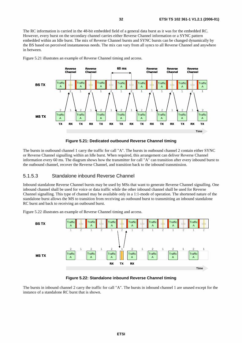
ETSI TS 102 361-1 V1.2.1 (2006-01) Technical Specification Electromagnetic compatibility and Radio spectrum Matters (ERM); Digital Mobile Radio (DMR) Systems; Part 1: DMR Air Interface (AI) protocol
Transcript
ETSI TS 102 361-1 V1.2.1 (2006-01)
Technical Specification
Electromagnetic compatibilityand Radio spectrum Matters (ERM);
Digital Mobile Radio (DMR) Systems;Part 1: DMR Air Interface (AI) protocol
ETSI
ETSI TS 102 361-1 V1.2.1 (2006-01) 2
Reference RTS/ERM-TGDMR-057-1
Keywords air interface, digital, PMR, protocol, radio
ETSI
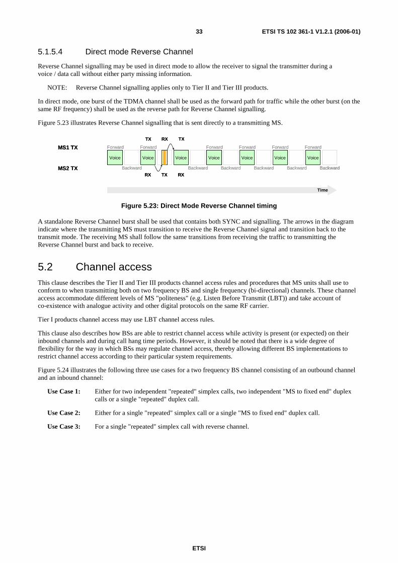
650 Route des Lucioles F-06921 Sophia Antipolis Cedex - FRANCE
Tel.: +33 4 92 94 42 00 Fax: +33 4 93 65 47 16
Siret N° 348 623 562 00017 - NAF 742 C
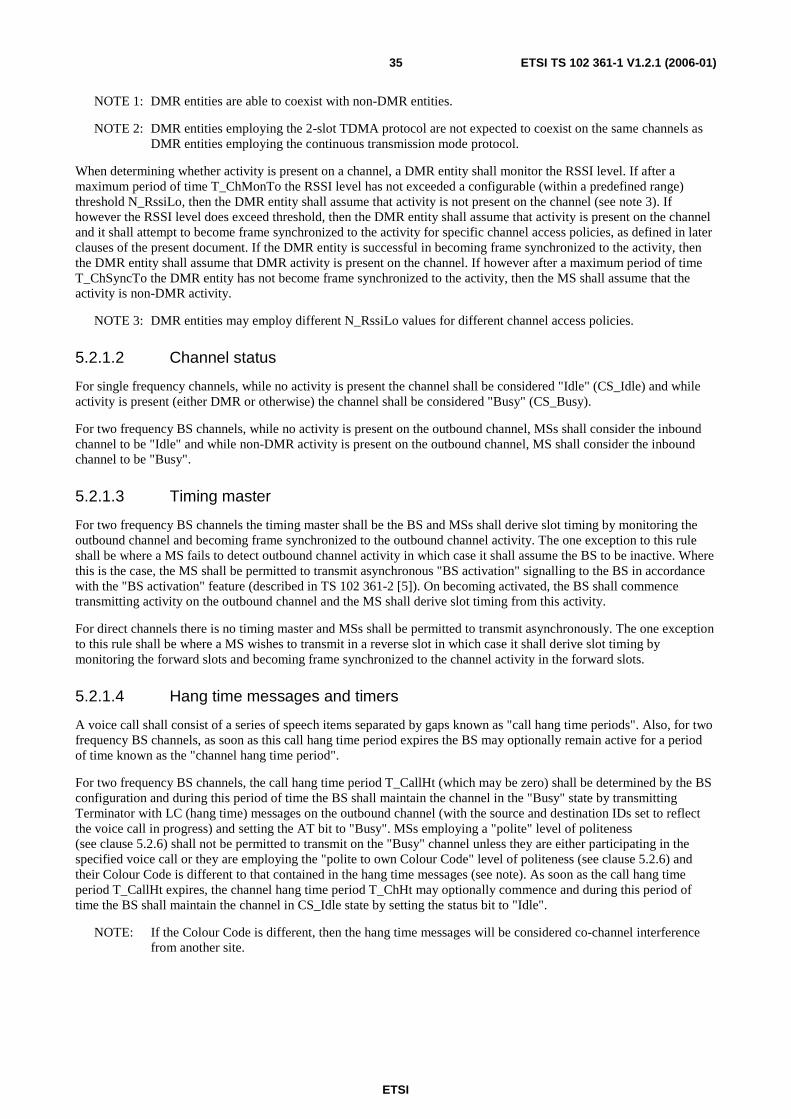
Association à but non lucratif enregistrée à la Sous-Préfecture de Grasse (06) N° 7803/88
Important notice
Individual copies of the present document can be downloaded from: http://www.etsi.org
The present document may be made available in more than one electronic version or in print. In any case of existing or perceived difference in contents between such versions, the reference version is the Portable Document Format (PDF).
In case of dispute, the reference shall be the printing on ETSI printers of the PDF version kept on a specific network drive within ETSI Secretariat.
Users of the present document should be aware that the document may be subject to revision or change of status. Information on the current status of this and other ETSI documents is available at
http://portal.etsi.org/tb/status/status.asp
If you find errors in the present document, please send your comment to one of the following services: http://portal.etsi.org/chaircor/ETSI_support.asp
Copyright Notification
No part may be reproduced except as authorized by written permission. The copyright and the foregoing restriction extend to reproduction in all media.
DECTTM, PLUGTESTSTM and UMTSTM are Trade Marks of ETSI registered for the benefit of its Members. TIPHONTM and the TIPHON logo are Trade Marks currently being registered by ETSI for the benefit of its Members. 3GPPTM is a Trade Mark of ETSI registered for the benefit of its Members and of the 3GPP Organizational Partners.
Intellectual Property Rights ................................................................................................................................8
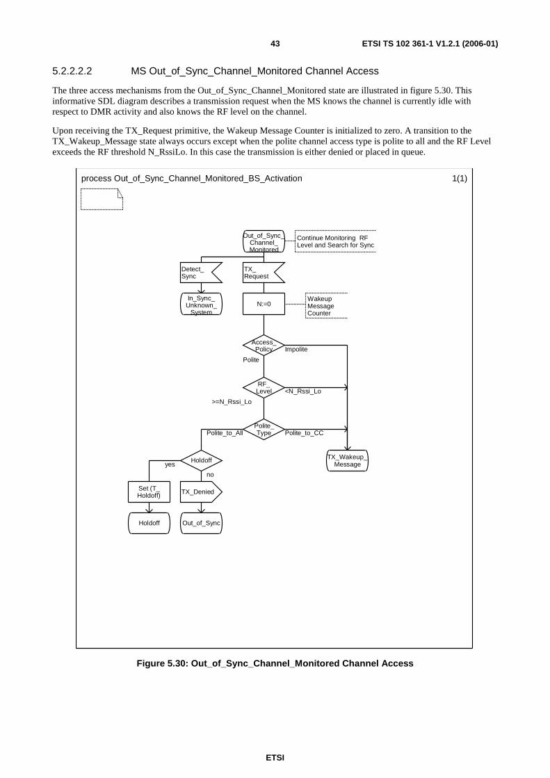
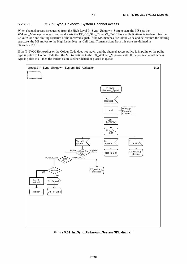
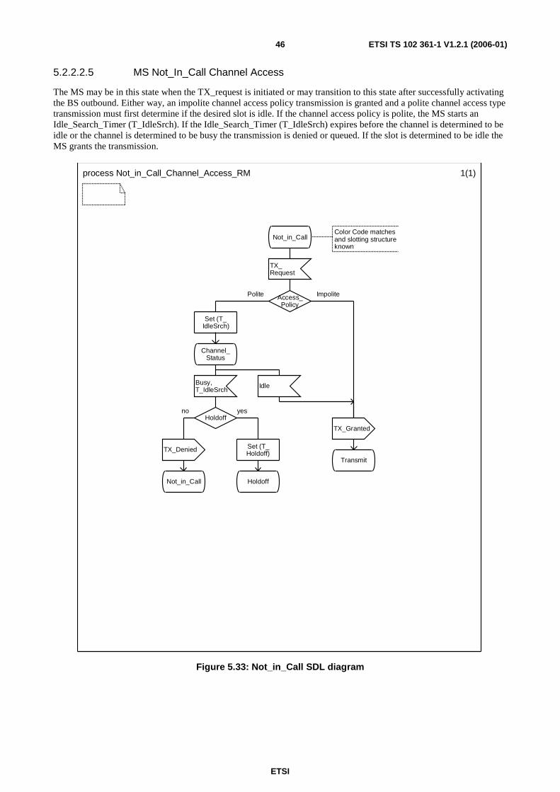
5.2.1.4 Hang time messages and timers ............................................................................................................35 5.2.1.5 Slot 1 and 2 dependency .......................................................................................................................36 5.2.1.6 Transmit admit criteria ..........................................................................................................................36 5.2.1.7 Transmission re-tries.............................................................................................................................36 5.2.2 Channel access procedure ...........................................................................................................................37 5.2.2.1 Peer to Peer Mode Channel Access.......................................................................................................37 5.2.2.1.1 MS Out_of_Sync Channel Access...................................................................................................37 5.2.2.1.2 MS Out_of_Sync_Channel_Monitored Channel Access.................................................................39 5.2.2.1.3 MS In_Sync_Unknown_System Channel Access ...........................................................................40 5.2.2.1.4 MS Not_in_Call Channel Access ....................................................................................................41 5.2.2.1.5 MS Others_Call Channel Access ....................................................................................................41 5.2.2.1.6 MS My_Call Channel Access..........................................................................................................41 5.2.2.2 Repeater Mode Channel Access............................................................................................................41 5.2.2.2.1 MS Out_of_Sync Channel Access...................................................................................................41 5.2.2.2.2 MS Out_of_Sync_Channel_Monitored Channel Access.................................................................43 5.2.2.2.3 MS In_Sync_Unknown_System Channel Access ...........................................................................44 5.2.2.2.4 MS TX_Wakeup_Message..............................................................................................................45 5.2.2.2.5 MS Not_In_Call Channel Access....................................................................................................46 5.2.2.2.6 MS Others_Call Channel Access ....................................................................................................47 5.2.2.2.7 MS My_Call Channel Access..........................................................................................................47 5.2.2.2.8 MS In_Session Channel Access ......................................................................................................47 5.2.2.3 Non-time critical CSBK ACK/NACK channel access..........................................................................47
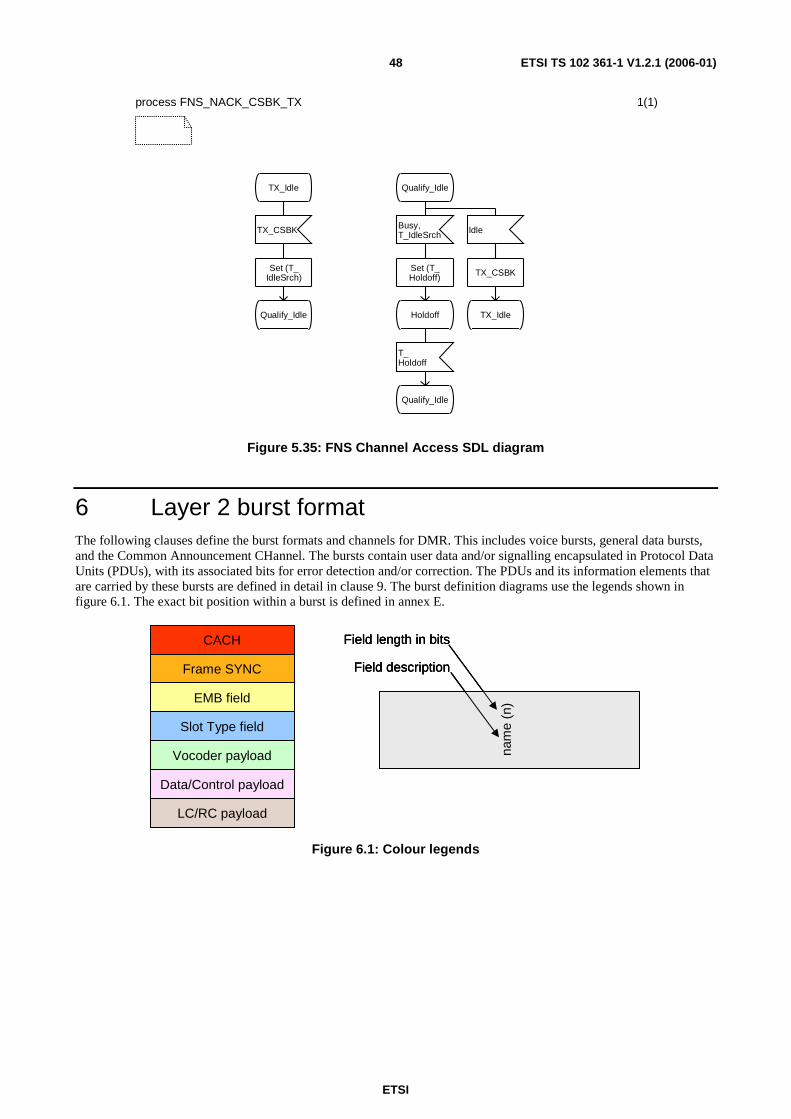
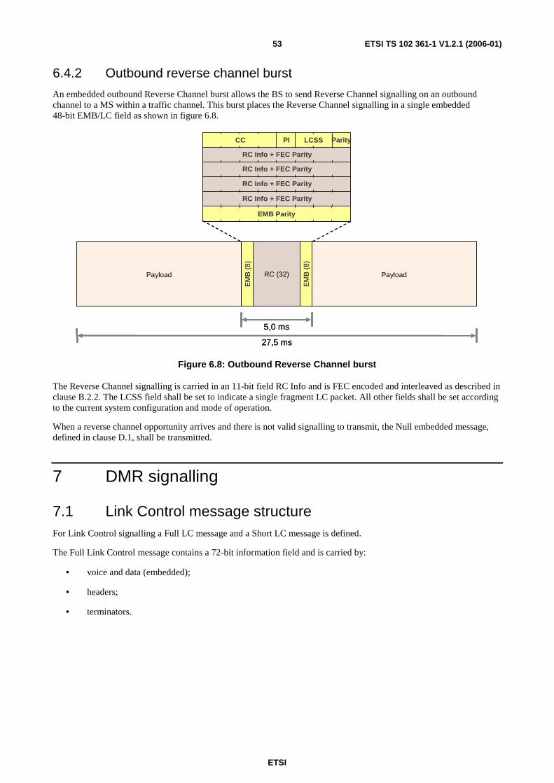
6 Layer 2 burst format ...............................................................................................................................48 6.1 Vocoder socket .................................................................................................................................................49 6.2 Data and control ...............................................................................................................................................50 6.3 Common Announcement Channel burst...........................................................................................................51 6.4 Reverse Channel...............................................................................................................................................52 6.4.1 Standalone inbound Reverse Channel burst................................................................................................52 6.4.2 Outbound reverse channel burst..................................................................................................................53
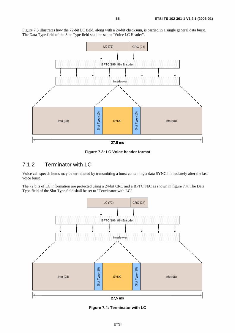
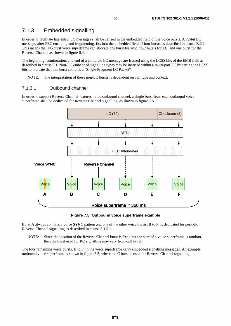
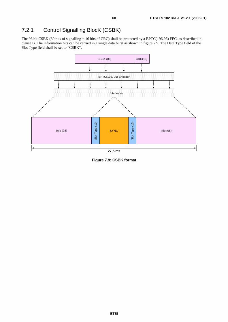
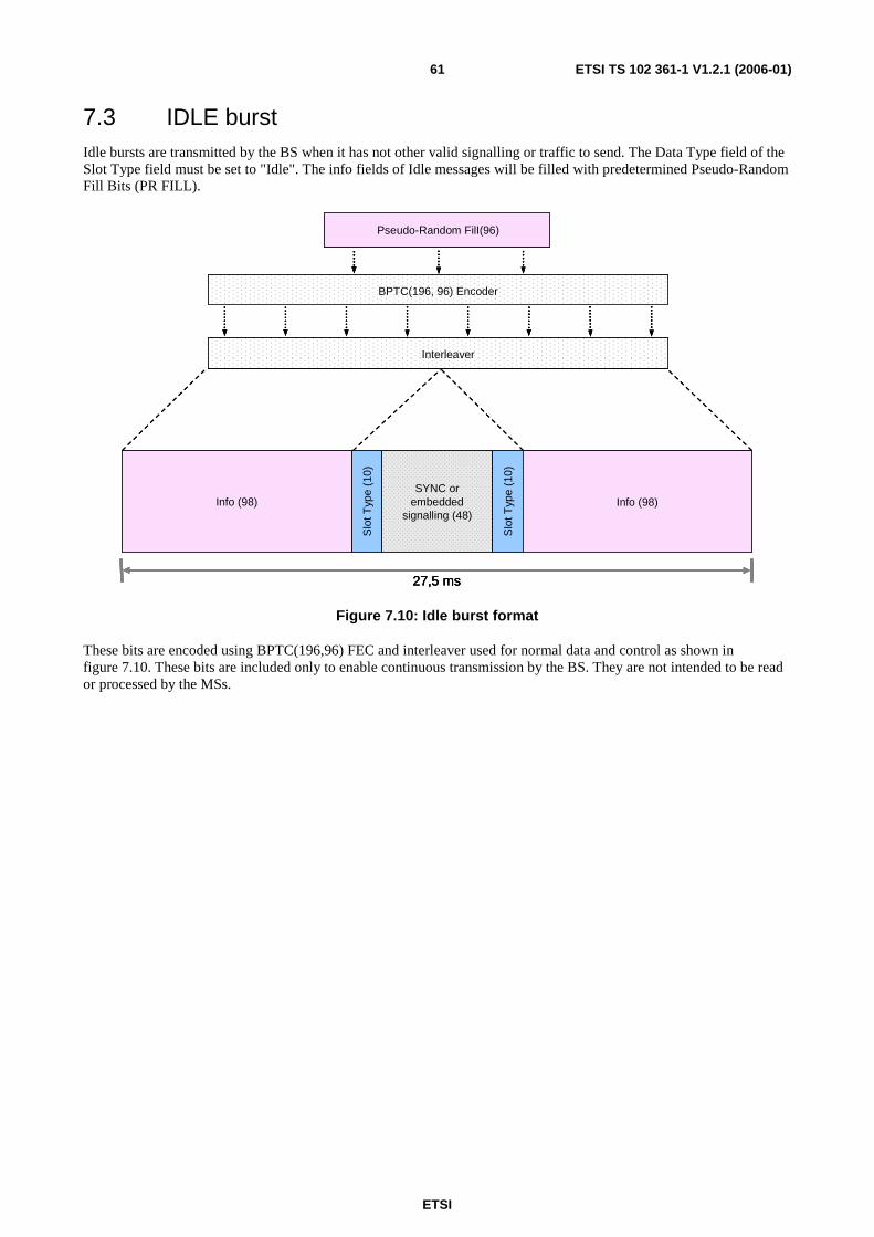
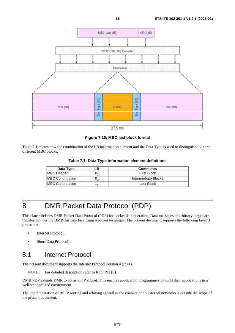
7 DMR signalling ......................................................................................................................................53 7.1 Link Control message structure........................................................................................................................53 7.1.1 Voice LC header .........................................................................................................................................54 7.1.2 Terminator with LC ....................................................................................................................................55 7.1.3 Embedded signalling...................................................................................................................................56 7.1.3.1 Outbound channel .................................................................................................................................56 7.1.3.2 Inbound channel ....................................................................................................................................57 7.1.4 Short Link Control in CACH......................................................................................................................58 7.2 Control Signalling BlocK (CSBK) message structure......................................................................................59 7.2.1 Control Signalling BlocK (CSBK) .............................................................................................................60 7.3 IDLE burst........................................................................................................................................................61 7.4 Multi Block Control (MBC) message structure................................................................................................62 7.4.1 Multi Block Control (MBC) .......................................................................................................................64
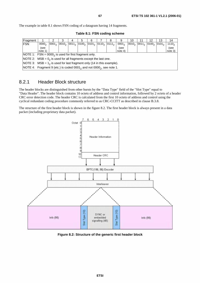
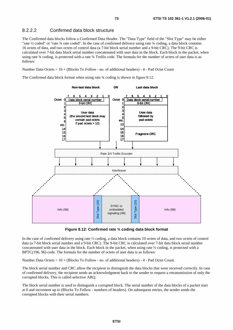
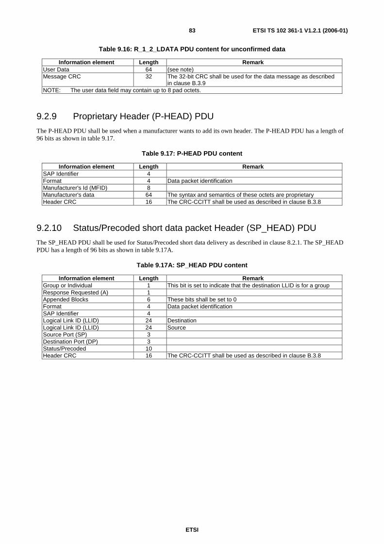
8 DMR Packet Data Protocol (PDP) .........................................................................................................65 8.1 Internet Protocol ...............................................................................................................................................65 8.2 Datagram fragmentation and re-assembly........................................................................................................66 8.2.1 Header Block structure ...............................................................................................................................67 8.2.1.1 Unconfirmed Data Header ....................................................................................................................68 8.2.1.2 Confirmed Data Header ........................................................................................................................68 8.2.1.3 Response Data Header ..........................................................................................................................69 8.2.1.4 Proprietary Data Header........................................................................................................................69 8.2.1.5 Status/precoded short data header .........................................................................................................70 8.2.1.6 Raw short data header ...........................................................................................................................70 8.2.1.7 Defined short data header......................................................................................................................71 8.2.1.8 Unified Data Transport (UDT) data header...........................................................................................71 8.2.2 Data block structure ....................................................................................................................................71 8.2.2.1 Unconfirmed data block structure .........................................................................................................72 8.2.2.2 Confirmed data block structure .............................................................................................................73 8.2.2.3 Response packet format ........................................................................................................................74 8.2.2.4 Hang time for Response packet.............................................................................................................75 8.2.2.5 Unified Data Transport (UDT) last data block structure.......................................................................76
ETSI
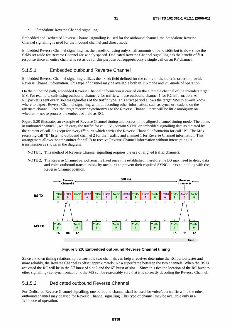
ETSI TS 102 361-1 V1.2.1 (2006-01) 5
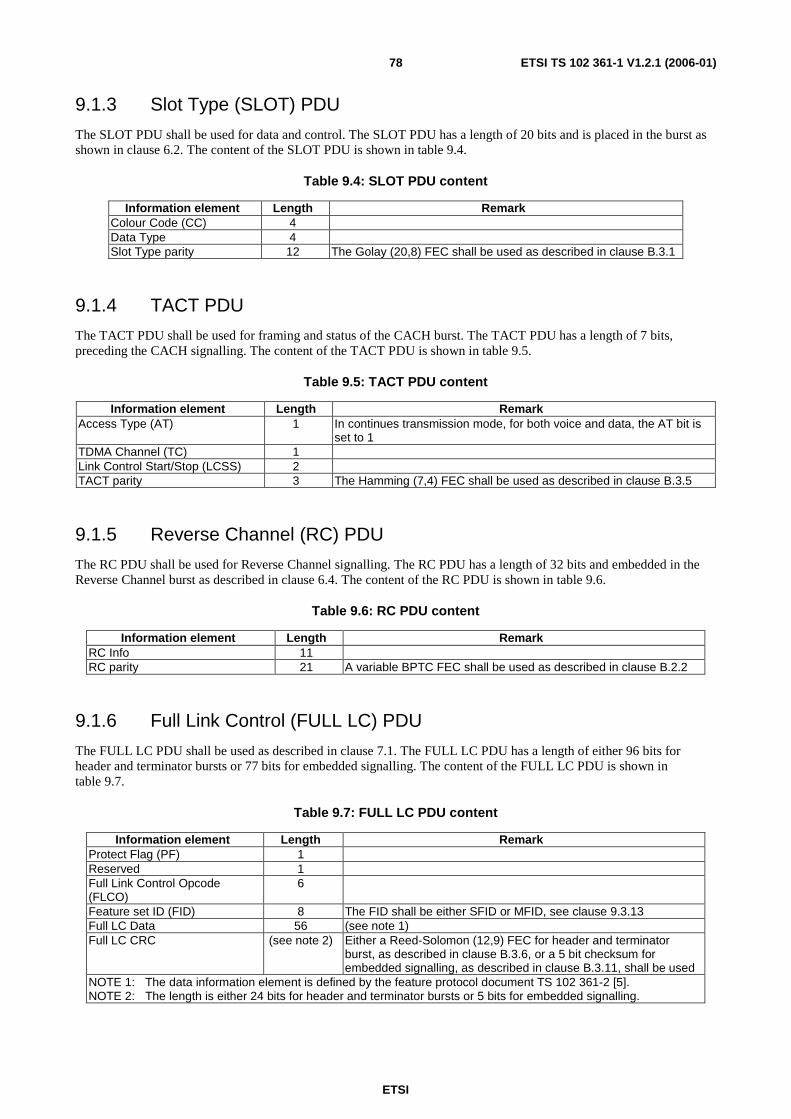
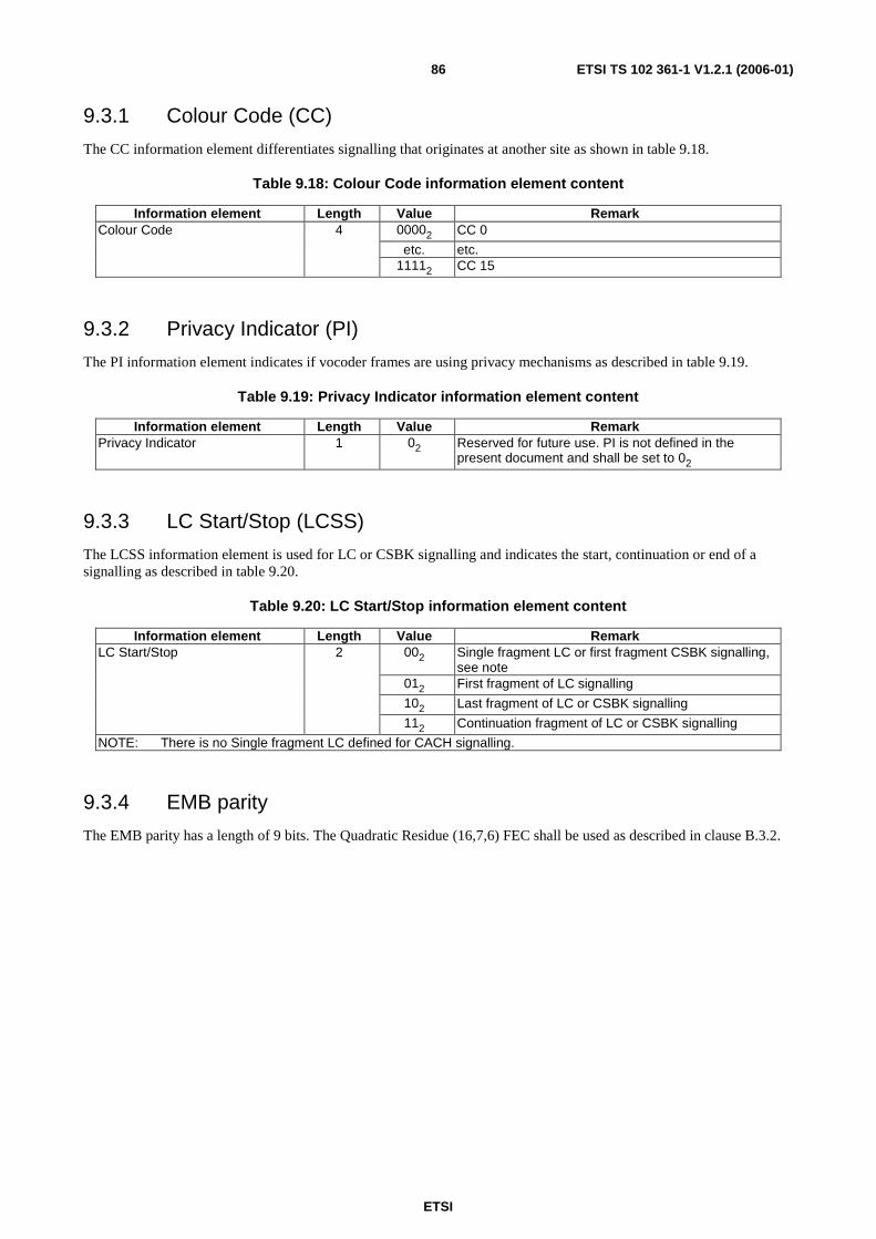
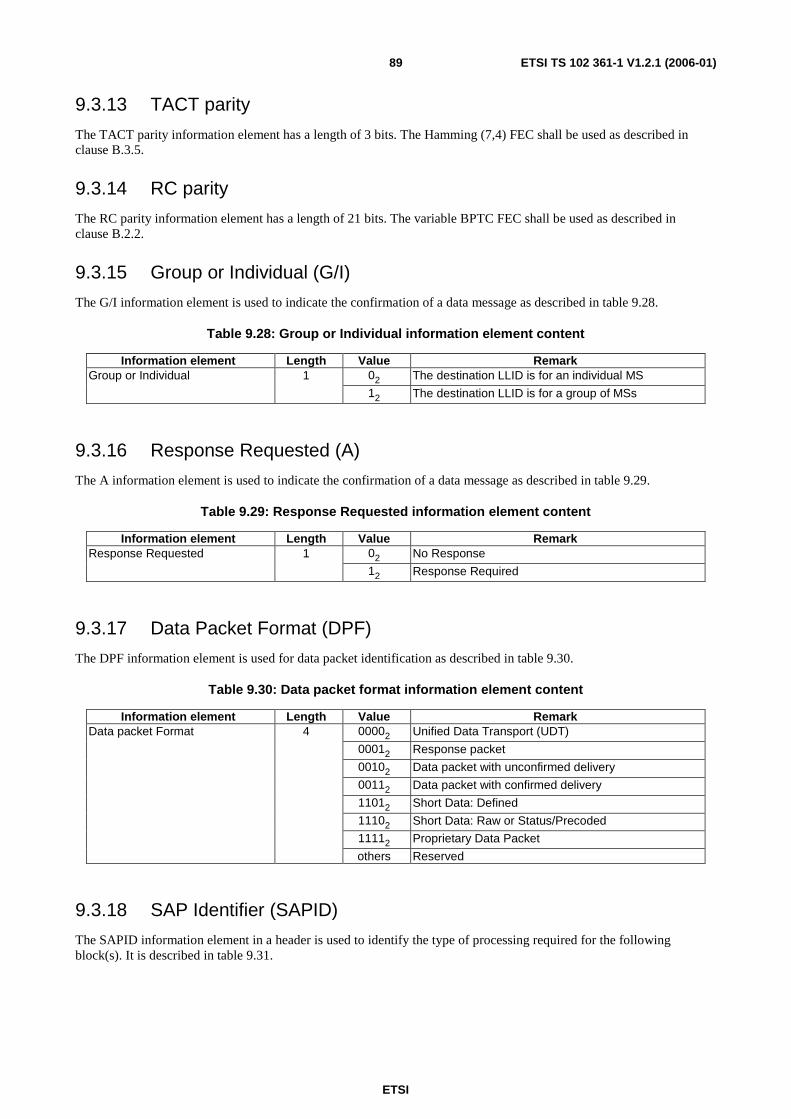
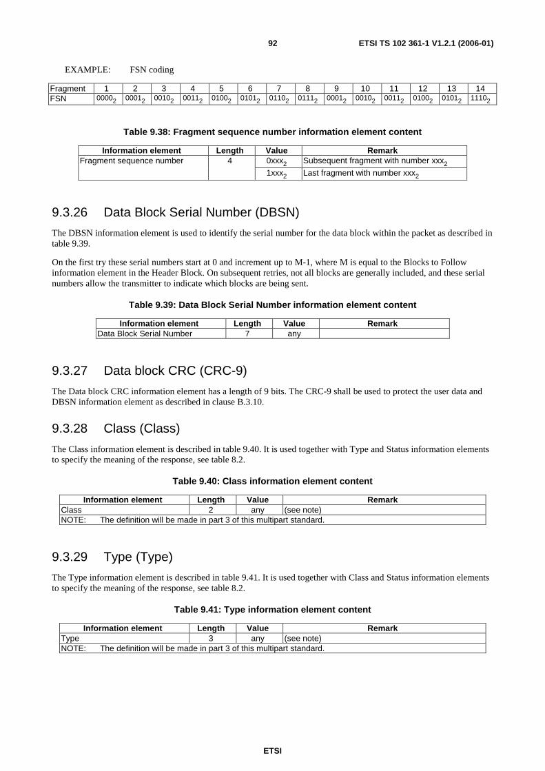
9 Layer 2 PDU description........................................................................................................................76 9.1 PDUs for voice bursts, general data bursts and the CACH ..............................................................................77 9.1.1 Synchronization (SYNC) PDU...................................................................................................................77 9.1.2 Embedded signalling (EMB) PDU .............................................................................................................77 9.1.3 Slot Type (SLOT) PDU ..............................................................................................................................78 9.1.4 TACT PDU.................................................................................................................................................78 9.1.5 Reverse Channel (RC) PDU .......................................................................................................................78 9.1.6 Full Link Control (FULL LC) PDU............................................................................................................78 9.1.7 Short Link Control (SHORT LC) PDU ......................................................................................................79 9.1.8 Control Signalling Block (CSBK) PDU .....................................................................................................79 9.1.9 Pseudo Random Fill Bit (PR FILL) PDU ...................................................................................................79 9.2 Data related PDU description...........................................................................................................................79 9.2.1 Confirmed packet Header (C_HEAD) PDU...............................................................................................80 9.2.2 Rate ¾ coded packet Data (R_3_4_DATA) PDU ......................................................................................80 9.2.3 Rate ¾ coded Last Data block (R_3_4_LDATA) PDU..............................................................................80 9.2.4 Confirmed Response packet Header (C_RHEAD) PDU ............................................................................81 9.2.5 Confirmed Response packet Data (C_RDATA) PDU ................................................................................81 9.2.6 Unconfirmed data packet Header (U_HEAD) PDU ...................................................................................82 9.2.7 Rate ½ coded packet Data (R_1_2_DATA) PDU ......................................................................................82 9.2.8 Rate ½ coded Last Data block (R_1_2_LDATA) PDU..............................................................................82 9.2.9 Proprietary Header (P-HEAD) PDU...........................................................................................................83 9.2.10 Status/Precoded short data packet Header (SP_HEAD) PDU ....................................................................83 9.2.11 Raw short data packet Header (R_HEAD) PDU ........................................................................................84 9.2.12 Defined Data short data packet Header (DD_HEAD) PDU .......................................................................84 9.2.13 Unified Data Transport Header (UDT_HEAD) PDU.................................................................................85 9.2.14 Unified Data Transport Last Data block (UDT_LDATA) PDU................................................................85 9.3 Layer 2 information element coding ................................................................................................................85 9.3.1 Colour Code (CC).......................................................................................................................................86 9.3.2 Privacy Indicator (PI)..................................................................................................................................86 9.3.3 LC Start/Stop (LCSS) .................................................................................................................................86 9.3.4 EMB parity .................................................................................................................................................86 9.3.5 Feature set ID (FID)....................................................................................................................................87 9.3.6 Data Type....................................................................................................................................................87 9.3.7 Slot Type parity ..........................................................................................................................................87 9.3.8 Access Type (AT).......................................................................................................................................88 9.3.9 TDMA Channel (TC)..................................................................................................................................88 9.3.10 Protect Flag (PF).........................................................................................................................................88 9.3.11 Full Link Control Opcode (FLCO) .............................................................................................................88 9.3.12 Short Link Control Opcode (SLCO)...........................................................................................................88 9.3.13 TACT parity................................................................................................................................................89 9.3.14 RC parity.....................................................................................................................................................89 9.3.15 Group or Individual (G/I) ...........................................................................................................................89 9.3.16 Response Requested (A) .............................................................................................................................89 9.3.17 Data Packet Format (DPF)..........................................................................................................................89 9.3.18 SAP Identifier (SAPID) ..............................................................................................................................89 9.3.19 Logical Link ID (LLID)..............................................................................................................................90 9.3.20 Full Message Flag (F) .................................................................................................................................90 9.3.21 Blocks to Follow (BF) ................................................................................................................................90 9.3.22 Pad Octet Count (POC)...............................................................................................................................90 9.3.23 Re-Synchronize Flag (S).............................................................................................................................91 9.3.24 Send sequence number (N(S)) ....................................................................................................................91 9.3.25 Fragment Sequence Number (FSN)............................................................................................................91 9.3.26 Data Block Serial Number (DBSN)............................................................................................................92 9.3.27 Data block CRC (CRC-9) ...........................................................................................................................92 9.3.28 Class (Class) ...............................................................................................................................................92 9.3.29 Type (Type) ................................................................................................................................................92 9.3.30 Status (Status) .............................................................................................................................................93 9.3.31 Last Block (LB) ..........................................................................................................................................93 9.3.32 Control Signalling BlocK Opcode (CSBKO) .............................................................................................93 9.3.33 Appended Blocks (AB)...............................................................................................................................93 9.3.34 Source Port (SP) .........................................................................................................................................93 9.3.35 Destination Port (DP)..................................................................................................................................94
ETSI
ETSI TS 102 361-1 V1.2.1 (2006-01) 6
9.3.36 Status/Precoded (S_P).................................................................................................................................94 9.3.37 Selective Automatic Repeat reQuest (SARQ) ............................................................................................94 9.3.38 Defined Data format (DD) ..........................................................................................................................94 9.3.39 Unified Data Transport Format (UDT Format) ..........................................................................................95 9.3.40 UDT Appended Blocks (UAB)...................................................................................................................96 9.3.41 Supplementary Flag (SF) ...........................................................................................................................96 9.3.42 Pad Nibble ..................................................................................................................................................96
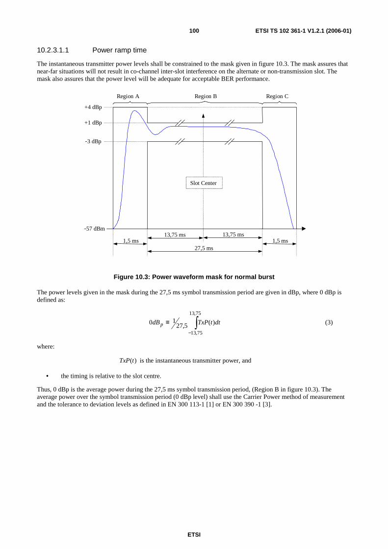
10 Physical Layer ........................................................................................................................................96 10.1 General parameters...........................................................................................................................................96 10.1.1 Frequency range..........................................................................................................................................96 10.1.2 RF carrier bandwidth ..................................................................................................................................96 10.1.3 Transmit frequency error ............................................................................................................................97 10.1.4 Time base clock drift error..........................................................................................................................97 10.2 Modulation .......................................................................................................................................................97 10.2.1 Symbols ......................................................................................................................................................97 10.2.2 4FSK generation .........................................................................................................................................97 10.2.2.1 Deviation index .....................................................................................................................................97 10.2.2.2 Square root raised cosine filter..............................................................................................................98 10.2.2.3 4FSK Modulator ...................................................................................................................................98 10.2.3 Burst timing ................................................................................................................................................99 10.2.3.1 Normal burst .........................................................................................................................................99 10.2.3.1.1 Power ramp time............................................................................................................................100 10.2.3.1.2 Symbol timing ...............................................................................................................................101 10.2.3.1.3 Propagation delay and transmission time ......................................................................................101 10.2.3.2 Reverse channel burst .........................................................................................................................102 10.2.3.2.1 Power ramp time............................................................................................................................102 10.2.3.2.2 Symbol timing ...............................................................................................................................103 10.2.3.2.3 Propagation delay ..........................................................................................................................103 10.2.3.3 Synthesizer Lock-Time constraints .....................................................................................................103 10.2.3.4 Transient frequency constraints during symbol transmission time .....................................................103
Annex A (normative): Numbering and addressing .........................................................................104
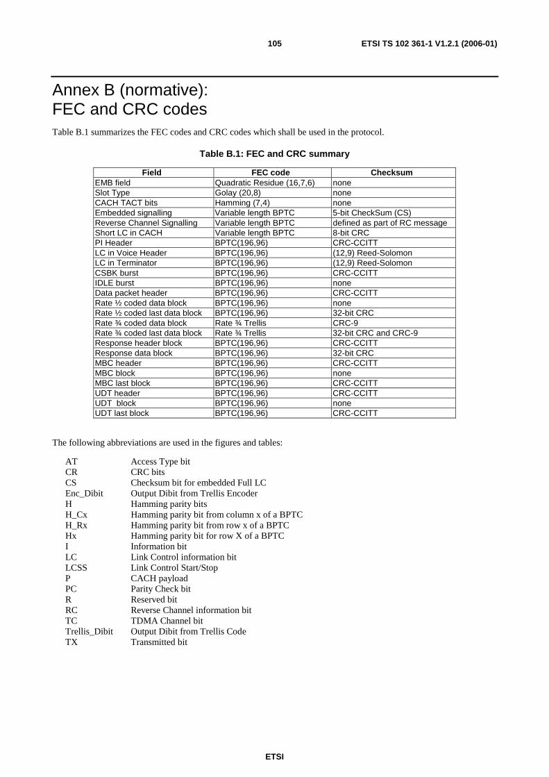
Annex B (normative): FEC and CRC codes ....................................................................................105
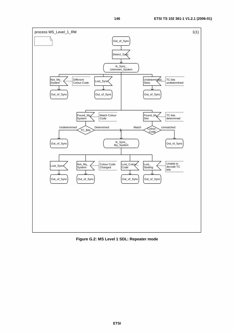
Annex G (informative): High level states overview ...........................................................................144
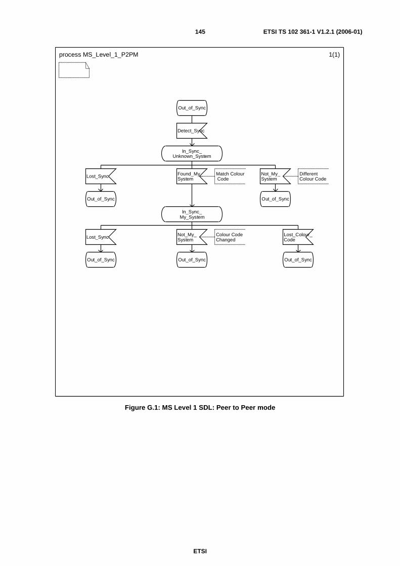
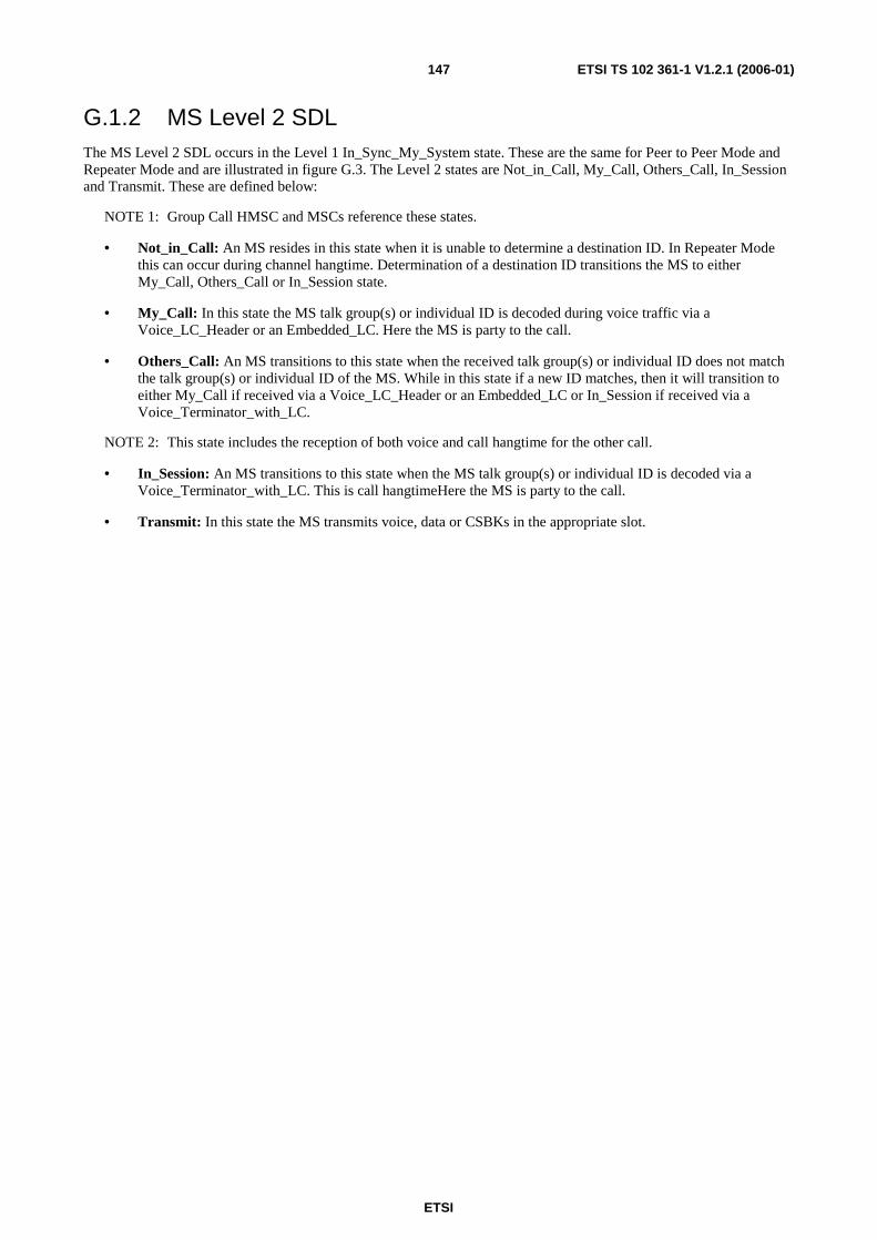
G.1 High Level MS states and SDL description .........................................................................................144 G.1.1 MS Level 1 SDL ............................................................................................................................................144 G.1.2 MS Level 2 SDL ............................................................................................................................................147
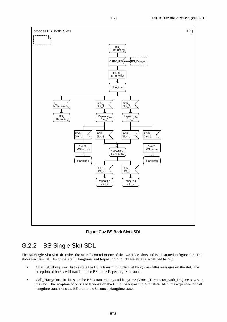
G.2 High Level BS states and SDL descriptions.........................................................................................149 G.2.1 BS Both Slots SDL.........................................................................................................................................149 G.2.2 BS Single Slot SDL........................................................................................................................................150
Annex H (normative): Feature interoperability ..............................................................................152
H.1 Feature set ID (FID) .............................................................................................................................152
H.2 Application for Manufacturer's Feature set ID.....................................................................................152
Annex I (informative): ETSI MFID application form .....................................................................153
History ............................................................................................................................................................156
ETSI
ETSI TS 102 361-1 V1.2.1 (2006-01) 8
Intellectual Property Rights IPRs essential or potentially essential to the present document may have been declared to ETSI. The information pertaining to these essential IPRs, if any, is publicly available for ETSI members and non-members, and can be found in ETSI SR 000 314: "Intellectual Property Rights (IPRs); Essential, or potentially Essential, IPRs notified to ETSI in respect of ETSI standards", which is available from the ETSI Secretariat. Latest updates are available on the ETSI Web server (http://webapp.etsi.org/IPR/home.asp).
Pursuant to the ETSI IPR Policy, no investigation, including IPR searches, has been carried out by ETSI. No guarantee can be given as to the existence of other IPRs not referenced in ETSI SR 000 314 (or the updates on the ETSI Web server) which are, or may be, or may become, essential to the present document.
Foreword This Technical Specification (TS) has been produced by ETSI Technical Committee Electromagnetic compatibility and Radio spectrum Matters (ERM).
The present document is part 1 of a multi-part deliverable covering the Technical Requirements for Digital Mobile Radio (DMR), as identified below:
Part 1: "DMR Air Interface (AI) protocol";
Part 2: "DMR voice and generic services and facilities";
1 Scope The present document contains technical requirements for Digital Mobile Radio (DMR) operating in the existing licensed land mobile service frequency bands, as identified in CEPT/ERC/T/R 25-08 [7].
The present document describes the Air Interface of a scalable Digital Mobile Radio system which covers three tiers of possible products:
Tier I: DMR equipment having an integral antenna and working in Direct Mode (unit-to-unit) under a general authorization with no individual rights operation.
Tier II: DMR systems operating under individual licences working in Direct Mode (unit-to-unit) or using a Base Station (BS) for repeating.
Tier III: DMR trunking systems under individual licences operating with a controller function that automatically regulates the communications.
NOTE : Tier II and Tier III products encompass both simulcast and non-simulcast systems.
The present document specifies the Air Interface, complying with either EN 300 113-1 [1] and EN 300 113-2 [2] or EN 300 390-1 [3] and EN 300 390-2 [4], that has been specifically developed with the intention of being suitable for all identified product tiers. A polite spectrum access protocol for sharing the physical channel has also been specified. Specifically, in this case for use in the existing land mobile service bands with the intention of causing minimum change to the spectrum planning and regulations. Thus the DMR protocol is intended to be applicable to the land mobile frequency bands, physical channel offset, duplex spacing, range assumptions and all other spectrum parameters without need for any change.
2 References The following documents contain provisions which, through reference in this text, constitute provisions of the present document.
• References are either specific (identified by date of publication and/or edition number or version number) or non-specific.
• For a specific reference, subsequent revisions do not apply.
• For a non-specific reference, the latest version applies.
Referenced documents which are not found to be publicly available in the expected location might be found at http://docbox.etsi.org/Reference.
[1] ETSI EN 300 113-1: "Electromagnetic compatibility and Radio spectrum Matters (ERM); Land mobile service; Radio equipment intended for the transmission of data (and/or speech) using constant or non-constant envelope modulation and having an antenna connector; Part 1: Technical characteristics and methods of measurement".
[2] ETSI EN 300 113-2: "Electromagnetic compatibility and Radio spectrum Matters (ERM); Land mobile service; Radio equipment intended for the transmission of data (and/or speech) using constant or non-constant envelope modulation and having an antenna connector; Part 2: Harmonized EN covering essential requirements under article 3.2 of the R&TTE Directive".
[3] ETSI EN 300 390-1: "Electromagnetic compatibility and Radio spectrum Matters (ERM); Land mobile service; Radio equipment intended for the transmission of data (and speech) and using an integral antenna; Part 1: Technical characteristics and test conditions".
[4] ETSI EN 300 390-2: "Electromagnetic compatibility and Radio spectrum Matters (ERM); Land mobile service; Radio equipment intended for the transmission of data (and speech) and using an integral antenna; Part 2: Harmonized EN covering essential requirements under article 3.2 of the R&TTE Directive".
[5] ETSI TS 102 361-2: "Electromagnetic compatibility and Radio spectrum Matters (ERM); Digital Mobile Radio (DMR) Systems; Part 2: DMR voice and generic services and facilities".
[7] CEPT/ERC/T/R 25-08: "Planning criteria and co-ordination of frequencies in the land mobile service in the range 29,7 to 921 MHz".
[8] IEC 61162-1: "Maritime navigation and radiocommunications equipment and systems - Digital interfaces - Part 1: Single talker and multiple listeners".
[9] ISO/IEC 646: "Information technology - ISO 7-bit coded character set for information interchange".
[11] ETSI TS 102 361-4: "Electromagnetic compatibility and Radio spectrum Matters (ERM); Digital Mobile Radio (DMR) Systems; Part 4: DMR trunking protocol".
[12] ETSI TS 102 361-3: "Electromagnetic compatibility and Radio spectrum Matters (ERM); Digital Mobile Radio (DMR) Systems; Part 3: DMR Data protocol".
3 Definitions, symbols and abbreviations
3.1 Definitions For the purposes of the present document, the following terms and definitions apply:
1:1-mode: 1 traffic channel mode
NOTE: 1:1-mode supports one "MS to fixed end" duplex call or one simplex call with an optional inbound Reverse Channel using a two frequency BS.
2:1-mode: 2 traffic channel mode
NOTE: 2:1-mode supports two independent calls which may be either "MS to fixed end" duplex calls or simplex calls using a two frequency BS.
backward: logical channel from target to source in direct mode
Base Station (BS): fixed end equipment that is used to obtain DMR services
bearer service: telecommunication service providing the capability for information transfer between access point
burst: elementary amount of bits within the physical channel
NOTE 1: Three different bursts exists with different number of bits. The Traffic burst contains 264 bits, the CACH burst contains 24 bits and the RC burst contains 96 bits.
NOTE 2: The burst may include a guard time at the beginning and end of the burst used for power ramp-up and ramp-down.
NOTE 3: For detailed burst definition see clause 4.2.1.
call: complete sequence of related transactions between MSs
NOTE: Transactions may be one or more bursts containing specific call related information.
Control plane (C-plane): part of the DMR protocol stack dedicated to control and data services
ETSI
ETSI TS 102 361-1 V1.2.1 (2006-01) 11
conventional: non-trunked communication
NOTE: This is a communication technique where any radio unit (MS) may communicate with one or more other radio units (MSs) without using a trunking protocol, and may be either in direct mode or using any additional equipment (e.g. BS).
Digital Mobile Radio (DMR): physical grouping that contains all of the mobile and/or fixed end equipment that is used to obtain DMR services
direct mode: mode of operation where MSs may communicate outside the control of a network
NOTE: This is communication technique where any radio unit (MS) may communicate with one or more other radio units (MSs) without the need for any additional equipment (e.g. BS). This is also called unit-to-unit or peer-to-peer.
duplex: a mode of operation by which information can be transferred in both directions and where the two directions are independent
NOTE: Duplex is also known as full duplex.
forward: logical channel from source to target in direct mode
frame: two continues time slots labelled 1 and 2
NOTE: A frame has a length of 60 ms.
inbound: MS to BS transmission
logical channel: distinct data path between logical endpoints
NOTE: The logical channels are labelled 1 and 2. The logical channel may consist of sub-channels, e.g. SYNC, embedded signalling, etc.
Mobile Station (MS): physical grouping that contains all of the mobile equipment that is used to obtain DMR mobile services
outbound: BS to MS transmission
payload: bits in the information field
physical channel: RF carrier who will be modulated with information bits of the bursts
NOTE: The RF carrier may be a single frequency or a duplex pair of frequencies. The physical channel of a DMR subsystem is required to support the logical channels.
polite protocol: "Listen Before Transmit" (LBT) protocol
NOTE: This is a medium access protocol that implements a LBT function in order to ensure that the channel is free before transmitting.
privacy: secret transformation
NOTE: Any transformation of transmitted information that is derived from a shared secret between the sender and receiver.
Protocol Data Unit (PDU): unit of information consisting of protocol control information (signalling) and possibly user data exchanged between peer protocol layer entities
Radio Frequency channel: radio frequency carrier (RF carrier)
NOTE: This is a specified portion of the RF spectrum. In DMR, the RF carrier separation is 12,5 kHz. The physical channel may be a single frequency or a duplex spaced pair of frequencies.
Received Signal Strength Indication (RSSI): root mean squared (rms) value of the signal received at the receiver antenna
Reverse Channel (RC): signalling burst from target to source
ETSI
ETSI TS 102 361-1 V1.2.1 (2006-01) 12
signalling: exchange of information specifically concerned with the establishment and control of connections, and with management, in a telecommunication network
simplex: mode of working by which information can be transferred in both directions but not at the same time
superframe: 6 continuous traffic bursts on a logical channel labelled "A" to "F"
NOTE: A superframe has a length of 360 ms and is used for voice traffic only.
time slot (or slot): elementary timing of the physical channel
NOTE: A timeslot has a length of 30 ms and will be numbered "1" or "2".
transmission: transfer period of bursts containing information or signalling
NOTE: The transmission may be continuous, i.e. multiple bursts transmission without ramp-up, ramp-down, or discontinuous, i.e. single burst transmission with ramp-up and ramp-down period.
trunking: network controlled communication
NOTE: This is a communication technique where any radio unit (MS) may communicate with one or more other radio units (MSs) using a trunking protocol and all MSs will be under control of a network.
User plane (U-plane): part of the DMR protocol stack dedicated to user voice services
vocoder socket: 216 bits vocoder payload
3.2 Symbols For the purposes of the present document, the following symbols apply:
dBm absolute power level relative to 1 mW, expressed in dB dBp Power relative to the average power transmitted over a burst in decibel Eb Energy per bit No Noise per Hz
3.3 Abbreviations For the purposes of the present document, the following abbreviations apply:
4FSK Four-level Frequency Shift Keying AI Air Interface ARP Address Resolution Protocol ARQ Automatic Retransmission reQuest AT Access Type BER Bit Error Rate BPTC Block Product Turbo Code BS Base Station
NOTE: A reference designating a fixed end device.
CACH Common Announcement CHannel CC Colour Code CCL Call Control Layer C-plane Control plane CR CRC bits CRC Cyclic Redundancy Checksum for data error detection CS CheckSum CSBK Control Signalling BlocK CSBKO CSBK Opcode D_Sync General Data Burst Sync DBSN Data Block Serial Number DD Defined Data format
ETSI
ETSI TS 102 361-1 V1.2.1 (2006-01) 13
Dibit 2 bits grouped together to represent a 4-level symbol DLL Data Link Layer DMR Digital Mobile Radio DPF Data Packet Format DT Data Type field for General Data Bursts EMB EMBedded signalling field Enc_Dibit output Dibit from trellis Encoder ERC European Radiocommunication Commitee FEC Forward Error Correction FID Feature set ID FLCO Full Link Control Opcode FSN Fragment Sequence Number GF Galois Field to calculate parity checks for a RS code Golay Golay Code parity check Golay Name of a standard error correction code H Hamming parity bits H_Cx Hamming parity bit from Column x of a BPTC H_Rx Hamming parity bit from Row x of a BPTC HMSC High level Message Sequence Chart Hx Hamming parity bit for row x of a BPTC I Information bit ID IDentifier IP Internet Protocol LB Last Block LBT Listen Before Transmit LC Link Control LCSS Link Control Start/Stop LLID Logical Link ID LSB Least Significant Bit MBC Multiple Block Control packets MFID Manufacturer's FID MS Mobile Station
NOTE: A reference designating a mobile or portable radio.
MSB Most Significant Bit N_LC Null LC bit Octet 8 bits grouped together, also called a byte P CACH payload PA Power Amplifier PABX Private Automatic Branch eXchange PC Parity Check bit PDP Packet Data Protocol PDU Protocol Data Unit PF Protect Flag PI Privacy Indicator PL Physical Layer POC Pad Octet Count PR FILL Pseudo-Random Fill Bits PSTN Public Switched Telephone Network QR Quadratic Residue Code Parity Check bit R Reserved bit R_Sync Reverse channel Sync RC Reverse Channel RF Radio Frequency rms root mean squared RS Reed-Solomon code RSSI Received Signal Strength Indication SAP Service Access Point
NOTE: Where a network provides a service.
SAPID SAP Identifier
ETSI
ETSI TS 102 361-1 V1.2.1 (2006-01) 14
SDL Specification and Description Language SFID Standards FID SLCO Short Link Control Opcode SYNC SYNChronization TACT TDMA Access Channel Type TC TDMA Channel TCP Transmission Control Protocol TDD Time Division Duplex TDMA Time Division Multiple Access Trellis code Type of error correcting code for modulation Trellis_Dibit output Dibit from Trellis code Tribit 3 bits grouped together into a symbol for a trellis code TX Transmitted bit UDP User Datagram Protocol UDT Unified Data Transport U-plane User plane V_Sync TDMA Voice burst Sync VS Vocoder Socket bit
4 Overview The present document describes a Digital Mobile Radio (DMR) system for Tier II and Tier III products which employs a Time Division Multiple Access (TDMA) technology with a 2-slot TDMA solution and RF carrier bandwidth of 12,5 kHz. Additionally, a DMR system for Tier I products is described which employs a continuous transmission variation of the above mentioned technology.
The present document describes the Physical Layer (PL) and the Data Link Layer (DLL) of the DMR Air Interface (AI). Radio equipments (fixed, mobile or portable) which conform to the present document shall be interoperable at the PL and DLL with equipment from other manufacturers. Radio equipment of the present document shall also comply with TS 102 361-2 [5].
Slot formats, field definitions, and timing are defined for voice traffic, data traffic, and control signalling. An overview of the TDMA timing is provided followed by the basic slot formats and bit definitions. This is followed by definitions of the payload and control fields. Finally, the details of the modulation and timing constraints are specified.
The present document will not provide the specification or operational detail for system implementations which include but are not limited to trunking, roaming, network management, vocoder, security, data, subsystems interfaces and data between private and public switched telephone networks. It describes only the appropriate access requirements compatible with the Air Interface.
NOTE: The DMR standard consists of a multi-part deliverable, which will be referred to in the present document if needed.
4.1 Protocol architecture The purpose of this clause is to provide a model where the different functions and processes are identified and allocated to different layers in the DMR protocol stack.
The protocol stack in this clause and all other related clauses describe and specify the interfaces, but these stacks do not imply or restrict any implementation.
The DMR protocol architecture which is defined herein follows the generic layered structure, which is accepted for reference description and specification of layered communication architectures.
The DMR standard defines the protocols for the following 3 layered model as shown in figure 4.1.
The base of the protocol stack is the Physical Layer (PL) which is the layer 1.
ETSI
ETSI TS 102 361-1 V1.2.1 (2006-01) 15
The Data Link Layer (DLL), which is the layer 2, shall handle sharing of the medium by a number of users. At the DLL, the protocol stack shall be divided vertically into two parts, the User plane (U-plane), for transporting information without addressing capability (e.g. voice or data stream), and the Control plane (C-plane) for signalling with addressing capability, as illustrated by figure 4.1.
The Call Control Layer (CCL), which is layer 3, lies in the C-plane and is responsible for control of the call (addressing, facilities, and etc.), provides the services supported by DMR, and supports the Data Service. U-plane access at layer 2 (DLL) supports voice service which is available in DMR. The Control Layer and the facilities and services offered by DMR are described in TS 102 361-2 [5].
AI Layer 2
AI Layer 1
Call Control Layer
Data Link Layer
Physical Layer
Voice payload
AI Layer 3
Data payload
Control plane User plane Call Control information Intrinsic services Data call control
Figure 4.1: DMR protocol stack
4.1.1 Air Interface Physical Layer (layer 1)
The Air Interface layer 1 shall be the physical interface. It shall deal with the physical burst, composed of bits, which is to be sent and/or received. The Physical Layer is described in clause 10.
The Air Interface layer 1 shall contain the following functions:
• modulation and demodulation;
• transmitter and receiver switching;
• RF characteristics;
• bits and symbol definition;
• frequency and symbol synchronization;
• burst building.
4.1.2 Air Interface Data Link Layer (layer 2)
The Air Interface layer 2 shall handle logical connections and shall hide the physical medium from the upper layers. The Data Link Layer is described in clauses 5 to 9.
The main functions are as follows:
• channel coding (FEC, CRC);
• interleaving, de-interleaving and bit ordering;
• acknowledgement and retry mechanism;
ETSI
ETSI TS 102 361-1 V1.2.1 (2006-01) 16
• media access control and channel management;
• framing, superframe building and synchronization;
• burst and parameter definition;
• link addressing (source and/or destination);
• interfacing of voice applications (vocoder data) with the PL;
• data bearer services;
• exchanging signalling and/or user data with the CCL.
4.1.3 Air Interface Call Control Layer (layer 3)
Air Interface layer 3 (CCL) is applicable only to the C-plane, and shall be an entity for the services and facilities supported by DMR on top of the layer 2 functionality. The Call Control Layer is described in TS 102 361-2 [5] and may have embedded intrinsic services associated to it.
The CCL provides the following functions:
• BS activation / deactivation;
• establishing, maintaining and terminating of calls;
• individual or group call transmission and reception;
• destination addressing (DMR IDs or gateway as appropriate);
• support of intrinsic services (emergency signalling, pre-emption, late entry, etc.);
• data call control;
• announcement signalling.
4.2 DMR TDMA Structure
4.2.1 Overview of burst and channel structure
The described solution is based on a 2-slot TDMA structure.
The physical resource available to the radio system is an allocation of the radio spectrum. The radio spectrum allocation shall be partitioned into Radio Frequency (RF) carriers with each RF carrier partitioned in time into frames and timeslots.
A DMR burst is a period of RF carrier that is modulated by a data stream. A burst therefore represents the physical channel of a timeslot. The physical channel of a DMR subsystem is required to support the logical channels.
A logical channel is defined as a logical communication pathway between two or more parties. The logical channels represent the interface between the protocol and the radio subsystem. The logical channels may be separated into two categories:
• the traffic channels carrying speech or data information, and
• control channels carrying signalling.
A generalized timing diagram of exchanges between the MS and the BS is shown in figure 4.2 where the slots for the two TDMA physical channels are labelled channel "1" and "2". Inbound transmission is labelled "MS TX" and outbound transmission is labelled "BS TX". This diagram is intended to illustrate a number of signalling features and timing relationships and does not represent a particular scenario.
NOTE: The example timing in figure 4.2 applies to a two frequency BS.
Figure 4.2: TDMA timing overview
Key points illustrated by the figure 4.2 include:
• While the BS is keyed up, the outbound channel is continuously transmitted, even if there is no information to send. Transmission on the inbound channel is stopped when an MS has no information to transmit.
• The inbound channel has an unused guard time between bursts to allow Power Amplifier (PA) ramping and propagation delay.
• The outbound channel has a Common Announcement CHannel (CACH) between bursts for traffic channel management (framing and access) as well as low speed signalling.
• Bursts have either a synchronization pattern or an embedded signalling field located in the centre of the burst. Placing the embedded signalling in the middle of a burst allows time for a transmitting MS to optionally transition to the outbound channel and recover Reverse Channel (RC) information.
Other key points, summarized below but not limited to, are as follows:
• The centre of the inbound and outbound bursts shall be time aligned.
• The channel 1 and 2 bursts in the inbound channel are offset 30 ms in time from the channel 1 and 2 bursts in the outbound channel. This number scheme allows a single channel identifier field in the outbound CACH to use the same channel number when referring to the inbound and outbound channels.
• Different SYNC patterns are used in voice bursts and data bursts to allow the receiver to differentiate between them. Different SYNC patterns are used for inbound and outbound channels to help the receiver reject co-channel interference.
• A Colour Code (CC) is present in the embedded signalling field and general data burst to provide a simple means of distinguishing overlapping sites, in order to detect co-channel interference.
NOTE: The CC is not used for addressing (individual or group).
• The location of the SYNC bursts in channel 1 is independent from the location of the SYNC bursts in channel 2. The location of SYNC bursts in the inbound channels is independent from the location of the SYNC bursts in the outbound channels.
• Voice transmissions use a superframe that is 6 bursts (360 ms) long with bursts labelled "A" to "F". Each superframe starts with a voice synchronization pattern in burst A.
• Data and control do not have a superframe structure. These bursts may contain a synchronization pattern and may also carry embedded signalling, such as Reverse Channel, when required.
ETSI
ETSI TS 102 361-1 V1.2.1 (2006-01) 18
4.2.2 Burst and frame structure
The generic burst structure consists of two 108-bit payload fields and a 48-bit synchronization or signalling field as shown in figure 4.3. Each burst has a total length of 30 ms but 27,5 ms are used for the 264 bits content, which is sufficient to carry 60 ms of compressed speech, using 216 bits payload.
30,0 ms
SYNC or embeddedsignalling
27,5 ms
5,0 ms
PayloadPayload
108 bits 108 bits48 bits
264 bits
30,0 ms30,0 ms
SYNC or embeddedsignalling
27,5 ms27,5 ms
5,0 ms5,0 ms
PayloadPayload
108 bits108 bits 108 bits108 bits48 bits48 bits
264 bits264 bits
Figure 4.3: Generic burst structure
For example, for a vocoder that uses 20 ms vocoder frames, the burst will carry three 72-bit vocoder frames (including FEC) plus a 48-bit synchronization word in a voice burst, that is 264 bits (27,5 ms) used for the burst contents.
NOTE: For data and control information the payload is reduced to two 98-bit payload which left a 20-bit field for additional Data Type field definition, as described in clause 6.2.
The centre of each burst has a field that carries either synchronization or embedded signalling. This field is placed in the middle of a burst to support Reverse Channel signalling (see clause 5.1.5).
On the inbound channel, the remaining 2,5 ms is used for guard time to allow for PA ramping and propagation delay, as shown in figure 4.4 for an inbound frame.
TDMAburstcenter
SYNC or embeddedsignalling
PayloadPayload
TDMAburstcenter
SYNC or embeddedsignalling
PayloadPayload
30,0 ms 30,0 ms
TDMA frame
Timeslot 1 Timeslot 2
2,5 ms
TDMAburstcenter
SYNC or embeddedsignalling
PayloadPayloadPayload
TDMAburstcenter
SYNC or embeddedsignalling
PayloadPayload
30,0 ms30,0 ms 30,0 ms30,0 ms
TDMA frameTDMA frame
Timeslot 1 Timeslot 2
2,5 ms2,5 ms
Figure 4.4: MS sourced TDMA frame
ETSI
ETSI TS 102 361-1 V1.2.1 (2006-01) 19
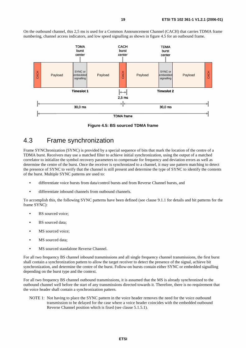
On the outbound channel, this 2,5 ms is used for a Common Announcement Channel (CACH) that carries TDMA frame numbering, channel access indicators, and low speed signalling as shown in figure 4.5 for an outbound frame.
SYNC or embeddedsignalling
PayloadPayloadSYNC or
embeddedsignalling
PayloadPayload
TDMAburstcenter
TDMAburstcenter
CACHburst
center
CA
CH
CA
CH
CA
CH
CA
CH
CA
CH
CA
CH
30,0 ms 30,0 ms
TDMA frame
Timeslot 1 Timeslot 2
2,5 ms
SYNC or embeddedsignalling
PayloadPayloadSYNC or
embeddedsignalling
PayloadPayload
TDMAburstcenter
TDMAburstcenter
CACHburst
center
CA
CH
CA
CH
CA
CH
CA
CH
CA
CH
CA
CH
CA
CH
CA
CH
CA
CH
CA
CH
30,0 ms30,0 ms 30,0 ms30,0 ms
TDMA frameTDMA frame
Timeslot 1 Timeslot 2
2,5 ms2,5 ms
Figure 4.5: BS sourced TDMA frame
4.3 Frame synchronization Frame SYNChronization (SYNC) is provided by a special sequence of bits that mark the location of the centre of a TDMA burst. Receivers may use a matched filter to achieve initial synchronization, using the output of a matched correlator to initialize the symbol recovery parameters to compensate for frequency and deviation errors as well as determine the centre of the burst. Once the receiver is synchronized to a channel, it may use pattern matching to detect the presence of SYNC to verify that the channel is still present and determine the type of SYNC to identify the contents of the burst. Multiple SYNC patterns are used to:
• differentiate voice bursts from data/control bursts and from Reverse Channel bursts, and
• differentiate inbound channels from outbound channels.
To accomplish this, the following SYNC patterns have been defined (see clause 9.1.1 for details and bit patterns for the frame SYNC):
• BS sourced voice;
• BS sourced data;
• MS sourced voice;
• MS sourced data;
• MS sourced standalone Reverse Channel.
For all two frequency BS channel inbound transmissions and all single frequency channel transmissions, the first burst shall contain a synchronization pattern to allow the target receiver to detect the presence of the signal, achieve bit synchronization, and determine the centre of the burst. Follow-on bursts contain either SYNC or embedded signalling depending on the burst type and the context.
For all two frequency BS channel outbound transmissions, it is assumed that the MS is already synchronized to the outbound channel well before the start of any transmissions directed towards it. Therefore, there is no requirement that the voice header shall contain a synchronization pattern.
NOTE 1: Not having to place the SYNC pattern in the voice header removes the need for the voice outbound transmission to be delayed for the case where a voice header coincides with the embedded outbound Reverse Channel position which is fixed (see clause 5.1.5.1).
ETSI
ETSI TS 102 361-1 V1.2.1 (2006-01) 20
NOTE 2: A SYNC pattern is always required in the data header and voice burst A, therefore the outbound transmission has to be delayed by a burst where either a data header or voice burst A would otherwise coincide with the embedded outbound Reverse Channel position.
For data and control messages, the embedded field shall be a data SYNC pattern except for special cases such as Reverse Channel signalling. For voice calls, the voice SYNC pattern occurs in the first burst of every voice superframe. In addition to marking the superframe boundaries, periodically inserting these periodic syncs allow late entry receivers to pick up voice messages after the transmission has started. See clause 5.1.2.1 for details on the superframe structure.
Figure 4.6 illustrates the best case and worst-case synchronization period for an inbound (MS to BS) TDMA channel. Since data and control messages contain a frame synchronization field in each burst, SYNC opportunities can occur as frequently as every 60 ms. During a voice call, SYNC opportunities occur every 360 ms, the length of a voice superframe. The first burst of every inbound transmission shall contain a SYNC pattern in order to allow the target to detect and synchronize to the transmission.
Figure 4.7 illustrates the best case and worst-case synchronization period for an outbound (BS to MS) TDMA channel. Because an outbound channel is continuously keyed, both TDMA channels always contain some type of signalling. In addition, since the target MS can receive both TDMA slots, the target MS can detect SYNC in either slot. Because data and control messages will typically contain a frame synchronization field in each burst, SYNC opportunities can occur as frequently as every 30 ms. During a voice call, SYNC opportunities occur every 360 ms, the length of a voice superframe, on each channel.
The figure 4.7 illustrates the worst-case SYNC timing for voice, 330 ms, which occurs when two voice calls are active and their superframes (for details of superframes see clause 5.1.2.1) are offset by 30 ms.
Based on these assumptions, the time between SYNC opportunities can be as short as 30 ms and as long as 330 ms.
When operating with a BS, a MS shall synchronize to an outbound channel and base its inbound timing entirely on the outbound timing. This insures that all MS units are working off of the same timing reference. If the BS is not currently transmitting, a MS wishing to access the system shall send a "BS activation" signalling to the BS asynchronously and wait for the outbound channel to be established before synchronizing and continuing with further transmission (see TS 102 361-2 [5]).
4.4.2 Direct mode timing relationship
In direct mode, the transmitting MS shall establish the timing reference. Any MS wishing to send Reverse Channel signalling back to the source shall synchronize to the forward path and shall base their Reverse Channel timing on the forward path timing. Once the source MS stops transmitting, any other MS wishing to transmit shall begin sending information asynchronously and establish a new and independent time reference.
NOTE: Reverse Channel signalling applies only for Tier II and Tier III products.
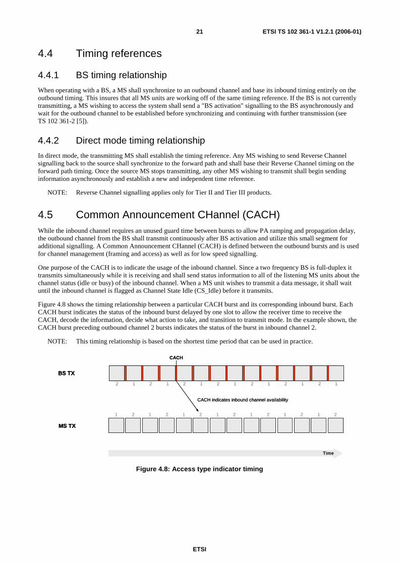
4.5 Common Announcement CHannel (CACH) While the inbound channel requires an unused guard time between bursts to allow PA ramping and propagation delay, the outbound channel from the BS shall transmit continuously after BS activation and utilize this small segment for additional signalling. A Common Announcement CHannel (CACH) is defined between the outbound bursts and is used for channel management (framing and access) as well as for low speed signalling.
One purpose of the CACH is to indicate the usage of the inbound channel. Since a two frequency BS is full-duplex it transmits simultaneously while it is receiving and shall send status information to all of the listening MS units about the channel status (idle or busy) of the inbound channel. When a MS unit wishes to transmit a data message, it shall wait until the inbound channel is flagged as Channel State Idle (CS_Idle) before it transmits.
Figure 4.8 shows the timing relationship between a particular CACH burst and its corresponding inbound burst. Each CACH burst indicates the status of the inbound burst delayed by one slot to allow the receiver time to receive the CACH, decode the information, decide what action to take, and transition to transmit mode. In the example shown, the CACH burst preceding outbound channel 2 bursts indicates the status of the burst in inbound channel 2.
NOTE: This timing relationship is based on the shortest time period that can be used in practice.
CACH
1 1 1 1 1 12 2 2 2 2 2 1 2
1 1 1 1 1 12 2 2 2 2 2 2 1
CACH indicates inbound channel availability
Time
MS TX
BS TX
CACH
1 1 1 1 1 12 2 2 2 2 2 1 2
1 1 1 1 1 12 2 2 2 2 2 2 1
CACH indicates inbound channel availability
TimeTime
MS TX
BS TX
MS TX
BS TX
Figure 4.8: Access type indicator timing
ETSI
ETSI TS 102 361-1 V1.2.1 (2006-01) 22
A second purpose of the CACH is to indicate the channel number of the inbound and outbound bursts as illustrated in figure 4.9. Each CACH burst defines the channel number for the outbound burst immediately following and the inbound burst delayed by one slot. In the example shown, the CACH burst indicates the position of inbound channel 2 and outbound channel 2.
1 1 1 1 1 12 2 2 2 2 2 1 2
1 1 1 1 1 12 2 2 2 2 2 2 1
CACH
CACH indicates inbound channel number
CACH indicates outbound channel number
Time
MS TX
BS TX
1 1 1 1 1 12 2 2 2 2 2 1 2
1 1 1 1 1 12 2 2 2 2 2 2 1
CACH
CACH indicates inbound channel number
CACH indicates outbound channel number
TimeTime
MS TX
BS TX
MS TX
BS TX
Figure 4.9: CACH channel indicator timing
A third purpose of the CACH is to carry additional low speed signalling as described in clause 7.1.4.
4.6 Basic channel types
4.6.1 Traffic channel with CACH
The traffic channel with CACH is shown in figure 4.10. This channel type shall be used for outbound transmissions from a two frequency BS to a MS. The channel consists of two TDMA traffic channels (channels 1 and 2) as well as a CACH for channel numbering, channel access, and low speed data. This channel is transmitted continuously without gaps as long as the BS is activated. If there is no information to transmit, the BS shall transmit Idle messages to fill out the bursts.
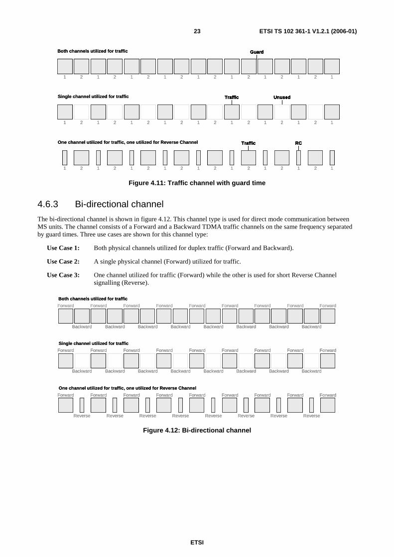
NOTE: This channel type should also be used for continuous transmission mode between MS units.
The traffic channel with guard time is shown in figure 4.11. This channel type shall be used for inbound transmissions from a MS to a two frequency BS (see note). The channel consists of two TDMA traffic channels (channels 1 and 2) separated by a guard time to allow PA ramping and propagation delay. Three use cases are shown for this channel type:
Use Case 1: Both channels utilized for traffic (see note).
Use Case 2: A single channel (channel 1) utilized for traffic.
Use Case 3: One channel utilized for traffic (channel 2) while the other is used for short standalone Reverse Channel bursts (channel 1).
NOTE: The first use case should also be used for communication via a single frequency BS where the Forward channel is MS to BS and the Backward channel is BS to MS.
ETSI
ETSI TS 102 361-1 V1.2.1 (2006-01) 23
Both channels utilized for traffic
Single channel utilized for traffic
One channel utilized for traffic, one utilized for Reverse Channel
Guard
UnusedTraffic
1 2 1 1 1 1 1 1 12 2 2 2 2 2 2 1
1 2 1 1 1 1 1 1 12 2 2 2 2 2 2 1
1 2 1 1 1 1 1 1 12 2 2 2 2 2 2 1
Traffic RC
Both channels utilized for traffic
Single channel utilized for traffic
One channel utilized for traffic, one utilized for Reverse Channel
The bi-directional channel is shown in figure 4.12. This channel type is used for direct mode communication between MS units. The channel consists of a Forward and a Backward TDMA traffic channels on the same frequency separated by guard times. Three use cases are shown for this channel type:
Use Case 1: Both physical channels utilized for duplex traffic (Forward and Backward).
Use Case 2: A single physical channel (Forward) utilized for traffic.
Use Case 3: One channel utilized for traffic (Forward) while the other is used for short Reverse Channel signalling (Reverse).
5 Layer 2 protocol description The following clauses describes the layer 2 protocol and defines the operation of the Data Link Layer (DLL) of the DMR Air Interface. The protocol description is made in terms of the timing relationship and the channel access rules.
5.1 Layer 2 timing
5.1.1 Channel timing relationship
The channel designation of "1" and "2" refer to physical channels that have a strictly defined relationship. The physical channel 1 and 2 bursts in the inbound channel are offset in time from the channel 1 and 2 bursts in the outbound channel. Various call types and services can require specific timing relationships between the inbound and outbound channels which lead to the definition of a number of logical channels.
Voice and data sessions require both an inbound and an outbound channel. These traffic channels can be either aligned in time (aligned channels) or non-aligned (offset channels) as described in clauses 5.1.1.1 and 5.1.1.2. MSs must be aware if aligned channel timing or offset channel timing is expected by the BS.
5.1.1.1 Aligned channel timing
Aligned timing supports Reverse Channel signalling by providing the receiving MS with a Reverse Channel transmit opportunity on the inbound channel without missing any of its outbound traffic.
NOTE 1: The physical channel numbers for inbound and outbound channels are different as shown in figure 5.1.
1 1 1 1 1 12 2 2 2 2 2 1 2
1 1 1 1 1 12 2 2 2 2 2 2 1
MS TX
BS TX
Time
1 1 1 1 1 12 2 2 2 2 2 1 2
1 1 1 1 1 12 2 2 2 2 2 2 1
MS TX
BS TX
TimeTime
Figure 5.1: Aligned channel timing
Aligned timing also supports "MS to MS" duplex traffic by allowing a MS to transmit in one timeslot and receive the repeated transmission of the other MS on the alternative timeslot.
NOTE 2: MS to MS timing requirements apply when communicating through a BS.
5.1.1.2 Offset channel timing
Offset timing supports "MS to fixed end" duplex traffic by allowing a MS to transmit in one time slot and receive the fixed end transmission on the alternate time slot.
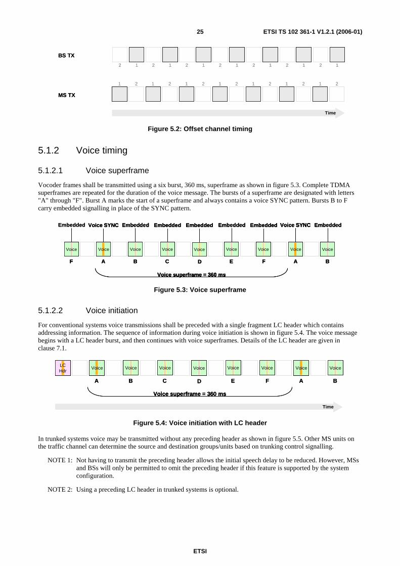
NOTE: The physical channel numbers for inbound and outbound channels are the same as shown in figure 5.2.
ETSI
ETSI TS 102 361-1 V1.2.1 (2006-01) 25
1 1 1 1 1 12 2 2 2 2 2 1 2
1 1 1 1 1 12 2 2 2 2 2 2 1
MS TX
BS TX
Time
1 1 1 1 1 12 2 2 2 2 2 1 2
1 1 1 1 1 12 2 2 2 2 2 2 1
MS TX
BS TX
TimeTime
Figure 5.2: Offset channel timing
5.1.2 Voice timing
5.1.2.1 Voice superframe
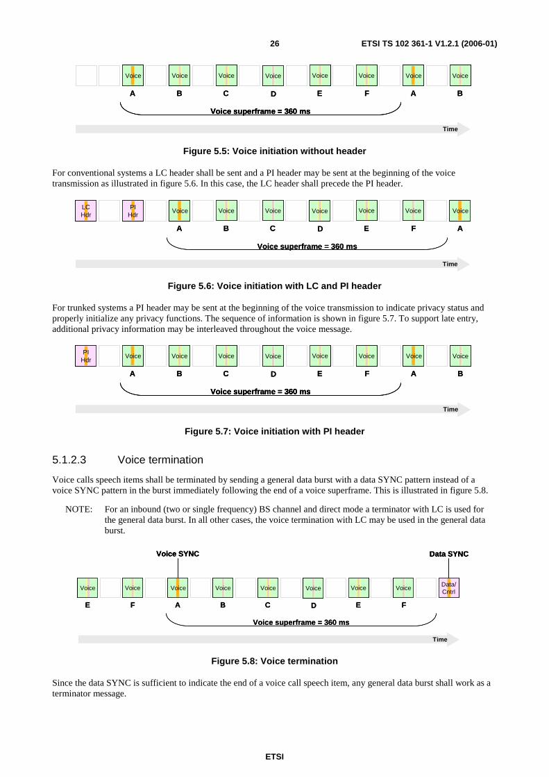
Vocoder frames shall be transmitted using a six burst, 360 ms, superframe as shown in figure 5.3. Complete TDMA superframes are repeated for the duration of the voice message. The bursts of a superframe are designated with letters "A" through "F". Burst A marks the start of a superframe and always contains a voice SYNC pattern. Bursts B to F carry embedded signalling in place of the SYNC pattern.
Voice superframe = 360 msVoice superframe = 360 ms
Figure 5.3: Voice superframe
5.1.2.2 Voice initiation
For conventional systems voice transmissions shall be preceded with a single fragment LC header which contains addressing information. The sequence of information during voice initiation is shown in figure 5.4. The voice message begins with a LC header burst, and then continues with voice superframes. Details of the LC header are given in clause 7.1.
Voice superframe = 360 msVoice superframe = 360 ms
TimeTime
Figure 5.4: Voice initiation with LC header
In trunked systems voice may be transmitted without any preceding header as shown in figure 5.5. Other MS units on the traffic channel can determine the source and destination groups/units based on trunking control signalling.
NOTE 1: Not having to transmit the preceding header allows the initial speech delay to be reduced. However, MSs and BSs will only be permitted to omit the preceding header if this feature is supported by the system configuration.
NOTE 2: Using a preceding LC header in trunked systems is optional.
Voice superframe = 360 msVoice superframe = 360 ms
TimeTime
Figure 5.5: Voice initiation without header
For conventional systems a LC header shall be sent and a PI header may be sent at the beginning of the voice transmission as illustrated in figure 5.6. In this case, the LC header shall precede the PI header.
Figure 5.6: Voice initiation with LC and PI header
For trunked systems a PI header may be sent at the beginning of the voice transmission to indicate privacy status and properly initialize any privacy functions. The sequence of information is shown in figure 5.7. To support late entry, additional privacy information may be interleaved throughout the voice message.
Voice superframe = 360 msVoice superframe = 360 ms
TimeTime
Figure 5.7: Voice initiation with PI header
5.1.2.3 Voice termination
Voice calls speech items shall be terminated by sending a general data burst with a data SYNC pattern instead of a voice SYNC pattern in the burst immediately following the end of a voice superframe. This is illustrated in figure 5.8.
NOTE: For an inbound (two or single frequency) BS channel and direct mode a terminator with LC is used for the general data burst. In all other cases, the voice termination with LC may be used in the general data burst.
Since the data SYNC is sufficient to indicate the end of a voice call speech item, any general data burst shall work as a terminator message.
ETSI
ETSI TS 102 361-1 V1.2.1 (2006-01) 27
5.1.3 Data timing
The present document defines single slot and dual slot data transmission modes. The differences between these two modes are only the bit rate offered to upper layers of the DMR stack leaving unchanged the format of the carried messages.
NOTE: It is a function of system implementation which data transmission modes are used.
5.1.3.1 Single slot data timing
Figure 5.9 illustrates one example of timing for single slot inbound data transmission. The single slot data transmission shall be initiated with one or two data headers that contain addressing as well as information about the payload. These headers are followed by one or more data blocks. The last block in the transmission contains payload and CRC to verify that the entire data message was successfully transferred. A complete description of the data transmission possibilities will be presented in TS 102 361-3 [12].
Figure 5.9 illustrates an exchange between a MS and the infrastructure where a single data header is required.
HdrDataBlock
DataBlock
DataBlock
DataBlock
LastBlock
HdrDataBlockDataBlock
DataBlockDataBlock
DataBlockDataBlock
DataBlockDataBlock
LastBlockLast
Block
Figure 5.9: Single header data timing
Figure 5.10 illustrates a single slot inbound data transmission exchange between two MS for which two data headers are required.
LastBlock
DataBlock
HdrHdrDataBlock
DataBlock
DataBlock
LastBlockLastBlock
DataBlockDataBlock
HdrHdrHdrHdrDataBlockDataBlock
DataBlockDataBlock
DataBlockDataBlock
Figure 5.10: Dual header data timing
The single slot data transmission mode is applicable to:
• direct channels; or
• single frequency repeater; or
• 1:1 repeater systems with reverse channel; or
• 1:1 repeater systems with no reverse channel; or
• 2:1 repeater systems.
5.1.3.2 Dual slot data timing
Figure 5.11 illustrates the timing for an outbound dual slot data occurrences. This example illustrates a transmission initiated with one data header. The header is followed by one or more data blocks (twelve in this example). The last block in the transmission contains payload and CRC to verify that the entire data message was successfully transferred.
NOTE: A complete description of the data transmission possibilities will be presented in TS 102 361-3 [12].
1 1 1 1 1 12 2 2 2 2 2 1
LastBlock
DataBlock
HdrDataBlock
DataBlock
DataBlock
DataBlock
DataBlock
DataBlock
DataBlock
DataBlock
DataBlock
DataBlock
1 1 1 1 1 12 2 2 2 2 2 1
LastBlock
DataBlock
HdrDataBlock
DataBlock
DataBlock
DataBlock
DataBlockDataBlock
DataBlockDataBlock
DataBlockDataBlock
DataBlockDataBlock
DataBlockDataBlock
DataBlock
Figure 5.11: Dual slot data timing
The dual slot data transmission mode is applicable to:
• direct channels; or
• 1:1 repeater systems with no reverse channel.
ETSI
ETSI TS 102 361-1 V1.2.1 (2006-01) 28
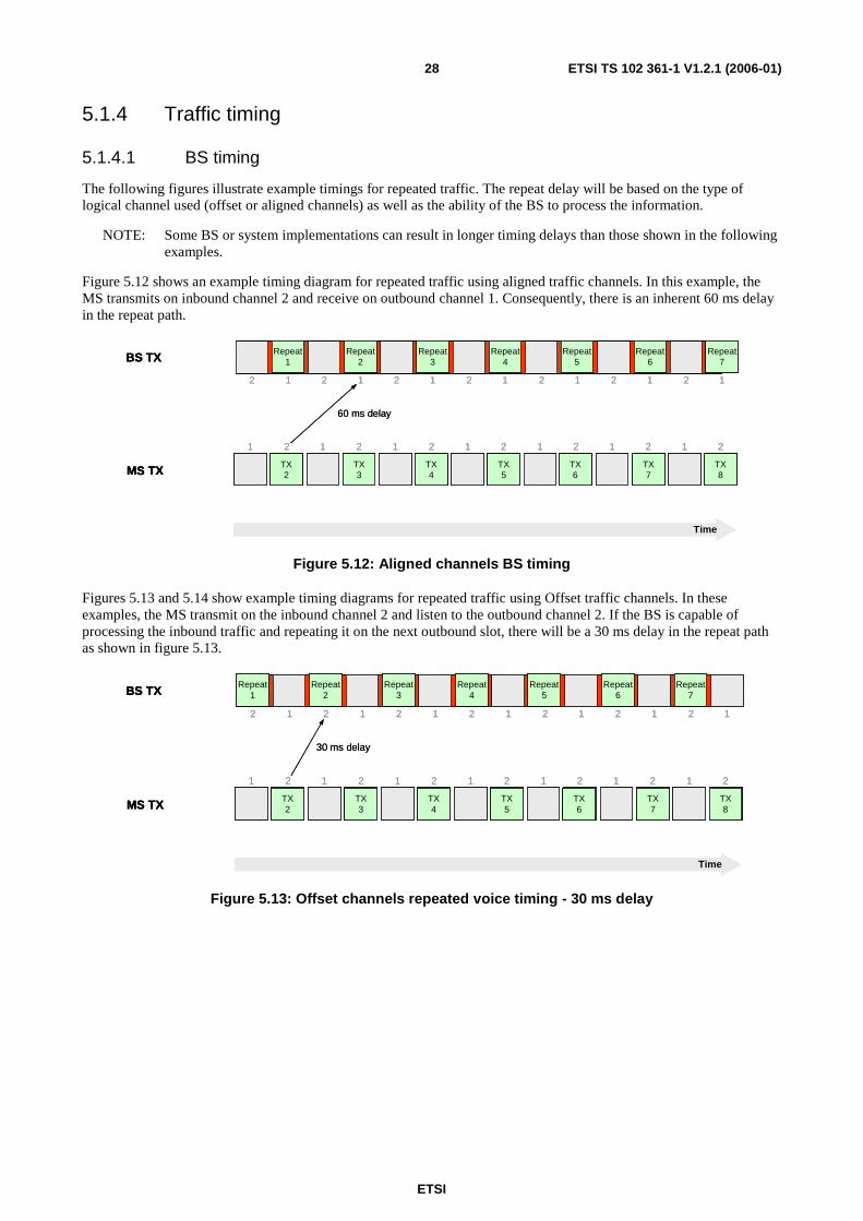
5.1.4 Traffic timing
5.1.4.1 BS timing
The following figures illustrate example timings for repeated traffic. The repeat delay will be based on the type of logical channel used (offset or aligned channels) as well as the ability of the BS to process the information.
NOTE: Some BS or system implementations can result in longer timing delays than those shown in the following examples.
Figure 5.12 shows an example timing diagram for repeated traffic using aligned traffic channels. In this example, the MS transmits on inbound channel 2 and receive on outbound channel 1. Consequently, there is an inherent 60 ms delay in the repeat path.
1 1 1 1 1 12 2 2 2 2 2 1 2
1 1 1 1 1 12 2 2 2 2 2 2 1
Time
MS TX
BS TX
TX2
TX3
TX4
TX5
TX6
TX7
TX8
Repeat1
Repeat2
Repeat3
Repeat4
Repeat5
Repeat6
Repeat7
60 ms delay
1 1 1 1 1 12 2 2 2 2 2 1 2
1 1 1 1 1 12 2 2 2 2 2 2 1
TimeTime
MS TX
BS TX
MS TX
BS TX
TX2
TX2
TX3
TX3
TX4
TX4
TX5
TX5
TX6
TX6
TX7
TX7
TX8
TX8
Repeat1
Repeat2
Repeat3
Repeat4
Repeat5
Repeat6
Repeat7
Repeat1
Repeat1
Repeat2
Repeat2
Repeat3
Repeat3
Repeat4
Repeat4
Repeat5
Repeat5
Repeat6
Repeat6
Repeat7
Repeat7
60 ms delay
Figure 5.12: Aligned channels BS timing
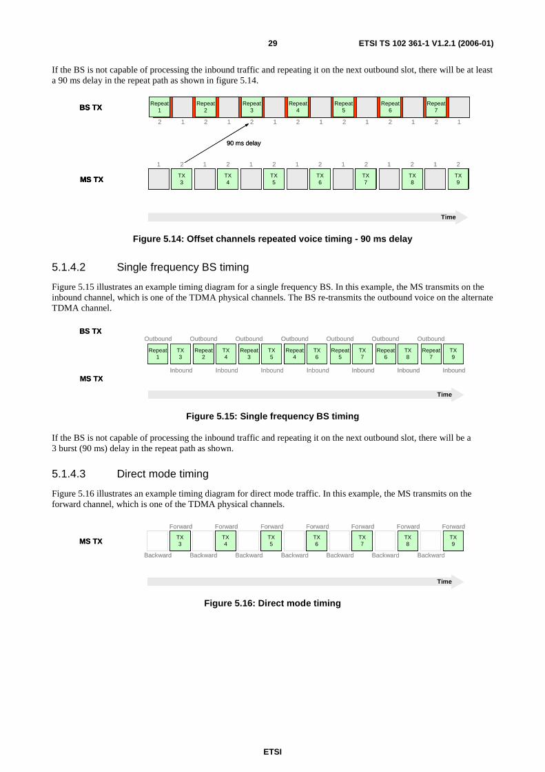
Figures 5.13 and 5.14 show example timing diagrams for repeated traffic using Offset traffic channels. In these examples, the MS transmit on the inbound channel 2 and listen to the outbound channel 2. If the BS is capable of processing the inbound traffic and repeating it on the next outbound slot, there will be a 30 ms delay in the repeat path as shown in figure 5.13.
If the BS is not capable of processing the inbound traffic and repeating it on the next outbound slot, there will be at least a 90 ms delay in the repeat path as shown in figure 5.14.
Figure 5.15 illustrates an example timing diagram for a single frequency BS. In this example, the MS transmits on the inbound channel, which is one of the TDMA physical channels. The BS re-transmits the outbound voice on the alternate TDMA channel.
If the BS is not capable of processing the inbound traffic and repeating it on the next outbound slot, there will be a 3 burst (90 ms) delay in the repeat path as shown.
5.1.4.3 Direct mode timing
Figure 5.16 illustrates an example timing diagram for direct mode traffic. In this example, the MS transmits on the forward channel, which is one of the TDMA physical channels.
Figure 5.17 shows an example timing diagram for TDD (duplex) voice. In this example, the MS transmits voice on inbound channel 2 and listen to voice on the outbound channel 2.
The format for Continuous Transmission uses the "Traffic Channel with CACH" defined in clause 4.6.1. In this mode, however, two traffic channels and the CACH are transmitted by a MS instead of a BS. In order to completely fill the channel, identical traffic is sent on both channel 1 and channel 2. Link Control signalling can be sent via the CACH if desired. Since there is no BS, only MS sourced SYNC patterns are used.
An example of continuous transmission for voice is illustrated in figure 5.18. This example shows a call initiated on channel 1 using an LC header, lasting a single voice superframe, and ending with a Terminator with LC. Voice traffic is sent using the inbound voice superframe defined in clause 5.1.2.1. Identical traffic is sent one burst later in channel 2 as shown.
Figure 5.18: Continuous transmission mode for voice
An example of continuous transmission for data is illustrated in figure 5.19. This example shows a data transaction on channel 1 initiated using the Enhanced Addressing Data Headers, lasting five data blocks, and ending with a Last Data Block. Identical traffic is sent one burst later in channel 2 as shown.
1 1 1 1 1 1 22 2 2 2 2 2 11 2
LastBlock
DataBlock
Hdr 2Hdr 1DataBlock
DataBlock
DataBlock
DataBlock
LastBlock
DataBlock
Hdr 2Hdr 1DataBlock
DataBlock
DataBlock
DataBlock
1 1 1 1 1 1 22 2 2 2 2 2 11 2
LastBlock
DataBlock
Hdr 2Hdr 1DataBlock
DataBlock
DataBlock
DataBlock
LastBlock
DataBlock
Hdr 2Hdr 1DataBlock
DataBlock
DataBlock
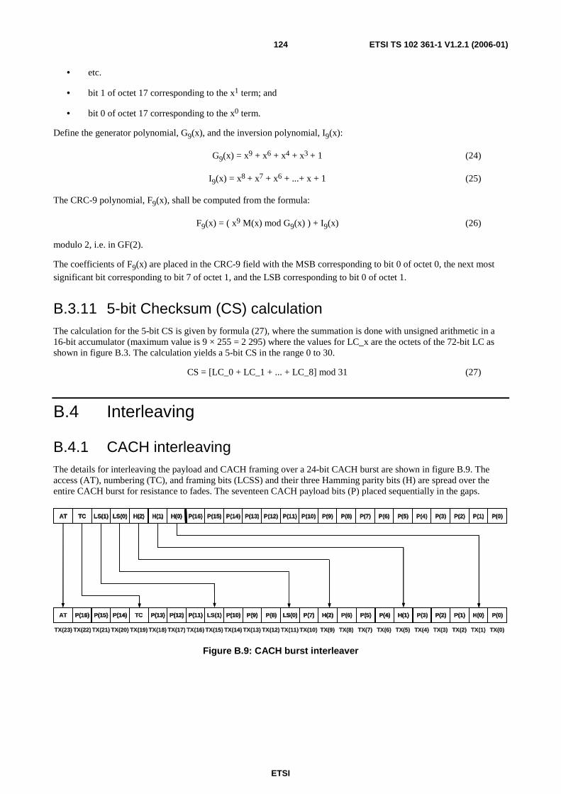
DataBlock
LastBlock
DataBlock
Hdr 2Hdr 1DataBlock
DataBlock
DataBlock
DataBlock
LastBlockLastBlock
DataBlockDataBlock
Hdr 2Hdr 2Hdr 1Hdr 1DataBlockDataBlock
DataBlockDataBlock
DataBlockDataBlock
DataBlockDataBlock
LastBlock
DataBlock
Hdr 2Hdr 1DataBlock
DataBlock
DataBlock
DataBlock
LastBlockLastBlock
DataBlockDataBlock
Hdr 2Hdr 2Hdr 1Hdr 1DataBlockDataBlock
DataBlockDataBlock
DataBlockDataBlock
DataBlockDataBlock
NOTE: If no CACH payload is available to transmit, "Null" LCs will be sent.
Figure 5.19: Continuous transmission mode for data
5.1.5 Reverse Channel timing
In order to support certain facilities, both the BS and MS units may send Reverse Channel signalling back to a source while it is transmitting. The following Reverse Channel signalling are defined:
• Embedded Reverse Channel signalling;
• Dedicated Reverse Channel signalling; and
ETSI
ETSI TS 102 361-1 V1.2.1 (2006-01) 31
• Standalone Reverse Channel signalling.
Embedded and Dedicated Reverse Channel signalling is used for the outbound channel, the Standalone Reverse Channel signalling is used for the inbound channel and direct mode.
Embedded Reverse Channel signalling has the benefit of using only small amounts of bandwidth but is slow since the fields set aside for Reverse Channel are widely spaced. Dedicated Reverse Channel signalling has the benefit of fast response since an entire channel is set aside for this purpose but supports only a single call on an RF channel.
5.1.5.1 Embedded outbound Reverse Channel
Embedded Reverse Channel signalling utilizes the 48-bit field defined for the centre of the burst in order to provide Reverse Channel information. This type of channel may be available both in 1:1-mode and 2:1-mode of operation.
On the outbound path, embedded Reverse Channel information is carried on the alternate channel of the intended target MS. For example, calls using outbound channel 2 for traffic will use outbound channel 1 for RC information. An RC packet is sent every 360 ms regardless of the traffic type. This strict period allows the target MSs to always know where to expect Reverse Channel signalling without decoding other information, such as syncs or headers, on the alternate channel. Once the target receiver synchronizes to the Reverse Channel, there will be little ambiguity on whether or not to process the embedded field as RC.
Figure 5.20 illustrates an example of Reverse Channel timing and access in the aligned channel timing mode. The bursts in outbound channel 1, which carry the traffic for call "A", contain SYNC or embedded signalling data as dictated by the content of call A except for every 6th burst which carries the Reverse Channel information for call "B". The MSs receiving call "B" listen to outbound channel 2 for their traffic and channel 1 for Reverse Channel information. This arrangement allows the transmitter for call B to receive Reverse Channel information without interrupting its transmission as shown in the diagram.
NOTE 1: This method of Reverse Channel signalling requires the use of aligned traffic channels.
NOTE 2: The Reverse Channel period remains fixed once it is established, therefore the BS may need to delay data and voice outbound transmissions by one burst to prevent their required SYNC bursts coinciding with the Reverse Channel position.
Since a known timing relationship between the two channels can help a receiver determine the RC period faster and more reliably, the Reverse Channel is offset approximately 1/2 a superframe between the two channels. When the BS is activated the RC will be in the 3rd burst of slot 2 and the 6th burst of slot 1. Since this ties the location of the RC burst to other signalling (i.e. synchronization), the MS can be reasonably sure that it is correctly decoding the Reverse Channel.
5.1.5.2 Dedicated outbound Reverse Channel
For Dedicated Reverse Channel signalling, one outbound channel shall be used for voice/data traffic while the other outbound channel may be used for Reverse Channel signalling. This type of channel may be available only in a 1:1-mode of operation.
ETSI
ETSI TS 102 361-1 V1.2.1 (2006-01) 32
The RC information is carried in the 48-bit embedded field of a general data burst as it was for the embedded RC. However, every burst on the secondary channel carries either Reverse Channel information or a SYNC pattern embedded within an Idle burst. The mix of Reverse Channel bursts and SYNC bursts can be changed dynamically by the BS based on perceived instantaneous needs. The mix can vary from all syncs to all Reverse Channel and anywhere in between.
Figure 5.21 illustrates an example of Reverse Channel timing and access.
The bursts in outbound channel 1 carry the traffic for call "A". The bursts in outbound channel 2 contain either SYNC or Reverse Channel signalling within an Idle burst. When required, this arrangement can deliver Reverse Channel information every 60 ms. The diagram shows how the transmitter for call "A" can transition after every inbound burst to the outbound channel, recover the Reverse Channel, and transition back to the inbound transmission.
5.1.5.3 Standalone inbound Reverse Channel
Inbound standalone Reverse Channel bursts may be used by MSs that want to generate Reverse Channel signalling. One inbound channel shall be used for voice or data traffic while the other inbound channel shall be used for Reverse Channel signalling. This type of channel may be available only in a 1:1-mode of operation. The shortened nature of the standalone burst allows the MS to transition from receiving an outbound burst to transmitting an inbound standalone RC burst and back to receiving an outbound burst.
Figure 5.22 illustrates an example of Reverse Channel timing and access.
The bursts in inbound channel 2 carry the traffic for call "A". The bursts in inbound channel 1 are unused except for the instance of a standalone RC burst that is shown.
ETSI
ETSI TS 102 361-1 V1.2.1 (2006-01) 33
5.1.5.4 Direct mode Reverse Channel
Reverse Channel signalling may be used in direct mode to allow the receiver to signal the transmitter during a voice / data call without either party missing information.
NOTE: Reverse Channel signalling applies only to Tier II and Tier III products.
In direct mode, one burst of the TDMA channel shall be used as the forward path for traffic while the other burst (on the same RF frequency) shall be used as the reverse path for Reverse Channel signalling.
Figure 5.23 illustrates Reverse Channel signalling that is sent directly to a transmitting MS.
A standalone Reverse Channel burst shall be used that contains both SYNC and signalling. The arrows in the diagram indicate where the transmitting MS must transition to receive the Reverse Channel signal and transition back to the transmit mode. The receiving MS shall follow the same transitions from receiving the traffic to transmitting the Reverse Channel burst and back to receive.
5.2 Channel access This clause describes the Tier II and Tier III products channel access rules and procedures that MS units shall use to conform to when transmitting both on two frequency BS and single frequency (bi-directional) channels. These channel access accommodate different levels of MS "politeness" (e.g. Listen Before Transmit (LBT)) and take account of co-existence with analogue activity and other digital protocols on the same RF carrier.
Tier I products channel access may use LBT channel access rules.
This clause also describes how BSs are able to restrict channel access while activity is present (or expected) on their inbound channels and during call hang time periods. However, it should be noted that there is a wide degree of flexibility for the way in which BSs may regulate channel access, thereby allowing different BS implementations to restrict channel access according to their particular system requirements.
Figure 5.24 illustrates the following three use cases for a two frequency BS channel consisting of an outbound channel and an inbound channel:
Use Case 1: Either for two independent "repeated" simplex calls, two independent "MS to fixed end" duplex calls or a single "repeated" duplex call.
Use Case 2: Either for a single "repeated" simplex call or a single "MS to fixed end" duplex call.
Use Case 3: For a single "repeated" simplex call with reverse channel.
Figure 5.25: Single frequency (bi-directional) channel
5.2.1 Basic channel access rules
5.2.1.1 Types of channel activity
When accessing a channel to transmit, a DMR entity (MS or BS) shall take account of the following types of activity which may already be present on the channel:
• DMR activity;
• other digital protocol activity (see notes 1 and 2);
• analogue activity (see note 1).
ETSI
ETSI TS 102 361-1 V1.2.1 (2006-01) 35
NOTE 1: DMR entities are able to coexist with non-DMR entities.
NOTE 2: DMR entities employing the 2-slot TDMA protocol are not expected to coexist on the same channels as DMR entities employing the continuous transmission mode protocol.
When determining whether activity is present on a channel, a DMR entity shall monitor the RSSI level. If after a maximum period of time T_ChMonTo the RSSI level has not exceeded a configurable (within a predefined range) threshold N_RssiLo, then the DMR entity shall assume that activity is not present on the channel (see note 3). If however the RSSI level does exceed threshold, then the DMR entity shall assume that activity is present on the channel and it shall attempt to become frame synchronized to the activity for specific channel access policies, as defined in later clauses of the present document. If the DMR entity is successful in becoming frame synchronized to the activity, then the DMR entity shall assume that DMR activity is present on the channel. If however after a maximum period of time T_ChSyncTo the DMR entity has not become frame synchronized to the activity, then the MS shall assume that the activity is non-DMR activity.
NOTE 3: DMR entities may employ different N_RssiLo values for different channel access policies.
5.2.1.2 Channel status
For single frequency channels, while no activity is present the channel shall be considered "Idle" (CS_Idle) and while activity is present (either DMR or otherwise) the channel shall be considered "Busy" (CS_Busy).
For two frequency BS channels, while no activity is present on the outbound channel, MSs shall consider the inbound channel to be "Idle" and while non-DMR activity is present on the outbound channel, MS shall consider the inbound channel to be "Busy".
5.2.1.3 Timing master
For two frequency BS channels the timing master shall be the BS and MSs shall derive slot timing by monitoring the outbound channel and becoming frame synchronized to the outbound channel activity. The one exception to this rule shall be where a MS fails to detect outbound channel activity in which case it shall assume the BS to be inactive. Where this is the case, the MS shall be permitted to transmit asynchronous "BS activation" signalling to the BS in accordance with the "BS activation" feature (described in TS 102 361-2 [5]). On becoming activated, the BS shall commence transmitting activity on the outbound channel and the MS shall derive slot timing from this activity.
For direct channels there is no timing master and MSs shall be permitted to transmit asynchronously. The one exception to this rule shall be where a MS wishes to transmit in a reverse slot in which case it shall derive slot timing by monitoring the forward slots and becoming frame synchronized to the channel activity in the forward slots.
5.2.1.4 Hang time messages and timers
A voice call shall consist of a series of speech items separated by gaps known as "call hang time periods". Also, for two frequency BS channels, as soon as this call hang time period expires the BS may optionally remain active for a period of time known as the "channel hang time period".
For two frequency BS channels, the call hang time period T_CallHt (which may be zero) shall be determined by the BS configuration and during this period of time the BS shall maintain the channel in the "Busy" state by transmitting Terminator with LC (hang time) messages on the outbound channel (with the source and destination IDs set to reflect the voice call in progress) and setting the AT bit to "Busy". MSs employing a "polite" level of politeness (see clause 5.2.6) shall not be permitted to transmit on the "Busy" channel unless they are either participating in the specified voice call or they are employing the "polite to own Colour Code" level of politeness (see clause 5.2.6) and their Colour Code is different to that contained in the hang time messages (see note). As soon as the call hang time period T_CallHt expires, the channel hang time period T_ChHt may optionally commence and during this period of time the BS shall maintain the channel in CS_Idle state by setting the status bit to "Idle".
NOTE: If the Colour Code is different, then the hang time messages will be considered co-channel interference from another site.
ETSI
ETSI TS 102 361-1 V1.2.1 (2006-01) 36
5.2.1.5 Slot 1 and 2 dependency
If a system is configured for 2:1-mode of operation, then both inbound slots shall be available for traffic and the "Busy" status for each inbound slot shall be independently controlled. For example, a voice or data call may be in progress on one slot while the other slot is "Idle".
If a system is configured for 1:1-mode of operation and the dual slot data capability is used, then both inbound slot 1 and 2 shall be used for traffic. The BS shall be able to set the status of each inbound slot to "Busy" or "Idle" according to the incoming slots.
In all other cases of a system is configured for 1:1-mode of operation, then inbound slot 2 shall be used for traffic and inbound slot 1 may provide the optional inbound reverse channel signalling opportunities. The BS shall be able to set the status of each inbound reverse channel signalling opportunity to CS_Busy or CS_Idle. When set to CS_Busy, an inbound reverse channel opportunity shall only be available to those MSs participating in the call in progress and when set to CS_Idle, an inbound Reverse Channel opportunity shall be available to all MSs.
5.2.1.6 Transmit admit criteria
Where a MS has been solicited to transmit a response, it may transmit the response in the expected time slot irrespective of whether the channel is CS_Idle or CS_Busy. Additionally, while a MS is partied to a voice call, it may transmit irrespective of whether the channel is CS_Idle or CS_Busy with DMR activity pertaining to the same voice call. However, for all other situations, subscribers shall be configurable to employ the following levels of "politeness" on a channel:
• Polite to all: The MS shall refrain from transmitting on a channel while the channel state is CS_Busy with other activity (either DMR or otherwise).
• Polite to own Colour Code: The MS shall refrain from transmitting on a channel while the channel state is CS_Busy with other DMR activity containing the MS's own (see note) Colour Code. For all other types of activity (including DMR activity containing a different Colour Code) already present on the channel, the MS shall transmit regardless.
• Impolite: The MS shall transmit on a channel regardless of any other activity (either DMR or otherwise) already present on the channel.
NOTE: This refers to the Colour Code that the MS intends embedding in its own transmission.
On a given channel, not all features may be supported the same level of politeness. So for example, voice transmissions may be configured to be "impolite" while packet data transmissions are configured to be "polite". Details of which levels of politeness are employed by which facilities are contained in TS 102 361-2 [5].
5.2.1.7 Transmission re-tries
Certain transmissions solicit responses and where these responses are not received (e.g. due to collisions, interference etc.) the transmitting entity may repeat the original transmission a number of times either until the response is received or the transmitting entity gives up.
For two frequency BS channels, a MS transmitting a message that requires a response from the BS shall wait for a configurable number of slots for the response (this configuration parameter shall allow for different system delays). However, a BS transmitting a message that requires a response from a MS shall expect to receive the response within a configurable number of slots (see note 1).
NOTE 1: The waiting times for re-transmission and the maximum number of re-tries are defined facility-by-facility basis in TS 102 361-2 [5].
For single frequency (bi-directional) channels (see note 2), a DMR entity (MS or BS) transmitting a message that requires a response from another DMR entity expect to receive the response in the next but one slot.
NOTE 2: This refers to direct channels.
ETSI
ETSI TS 102 361-1 V1.2.1 (2006-01) 37
In all cases, if a response is not received within the expected number of slots, then the DMR entity shall repeat the message a number of times (each time waiting for a response) either until a response is received, the message has been repeated a maximum number of times or unexpected DMR activity is detected (i.e. DMR activity not related to the original message). If a response is eventually received, the procedure shall have concluded successfully, otherwise if no response is received or unexpected DMR activity is detected (see note), then the procedure shall have failed (see note 1).
NOTE 3: Where unexpected DMR activity is detected, certain facilities (e.g. data) may require a random back-off and re-try procedure.
5.2.2 Channel access procedure
The basic channel access rules are given in clause 5.2.1. This clause of the present document expands upon these rules and uses informative SDL diagrams where necessary to illustrate and highlight specific points in both peer to peer mode and repeater mode. Both peer to peer and repeater modes support impolite, polite to own colour code and polite to all channel access mechanisms. Repeater mode also supports a BS outbound activation mechanism that is initiated by the MS.
The different MS high level states as defined in annex G are used as the starting MS states when a transmission is requested. Channel access can also be requested from the Out_of_Sync_Channel_Monitored state (PS_OutOfSyncChMon), which is a substate of the Out_of_Sync state (PS_OutOfSync). For non-time critcal applications the MS may also transition to the Holdoff state (PS_Holdoff) while waiting for the channel to become CS_Idle. These states are defined below:
• Out_of_Sync_Channel_Monitored (PS_OutOfSyncChMon): An MS transitions to this state from PS_OutOfSync after it has been monitoring the RF level and has not found SYNC for a duration of time long enough to establish knowledge of the channel. This time limit is established by the Monitor timer T_Monitor. After the expiration of this timer the MS has determined the channel is idle with respect to DMR activity. In this state the MS continues to monitor the RF level and search for SYNC.
• Holdoff (PS_Holdoff): An MS transitions to this state when a non-time critical transmission is requested and the channel is busy. Here the transmission request is queued by the MS. If a random holdoff is required the MS starts a random holdoff timer T_Holdoff. The services that allow a transmission to enter this state are defined in TS 102 361-2 [5].
NOTE: T_Holdoff is started for non-time critical transmissions.
5.2.2.1 Peer to Peer Mode Channel Access
In peer to peer mode it is possible to initiate channel access from any of the high level MS states as defined in annex G. These high level states include PS_OutOfSync, PS_InSyncUnknownSystem, PS_NotInCall and PS_OthersCall or PS_MyCall. It is also possible to request channel access while in PS_OutOfSyncChMon.
5.2.2.1.1 MS Out_of_Sync Channel Access
The three access mechanisms from the High Level MS Out_of_Sync state are illustrated in figure 5.26. This is an informative SDL diagram that generically shows transmission request from the Out_of_Sync state. In the Out_of_Sync state the MS has not resided on the channel long enough to immediately know the status of the channel. Therefore it must attempt to qualify the channel status. Additionally for completeness, figure 5.26 shows how transitions from Out_of_Sync state to either Out_of_Sync_Channel_Monitored or In_Sync_Unknown_System states occur. States not defined in the MS High Level SDL sections are Out_of_Sync_Find_Sync and In_Sync_Unknown_System_Find_CC. These are defined below:
• Out_of_Sync_Find_Sync: After a MS has determined RF is present on the channel it transitions to this state and attempts to synchronize to the signal. Expiration of the Monitor Timer T_Monitor while in this state implies the channel activity is non-DMR. For simplicity, this is illustrated as Find_Sync in the following informative SDL diagrams.
• In_Sync_Unknown_System_Find_CC: After a MS has synchronized to the channel it transitions to this state and attempts to decode the Colour Code present on the channel. Expiration of the TX_CC_Timer (T_TxCC) while in this state implies the channel activity is for a different system. For simplicity, this is illustrated as Find_CC in the following informative SDL diagrams.
ETSI
ETSI TS 102 361-1 V1.2.1 (2006-01) 38
A transmission request employing impolite channel access from the High Level MS Out_of_Sync state is always granted.
A transmission request employing either type of polite channel access policy from the High Level Out_of_Sync state will first measure the RF level present on the channel. If the measured RF level is less than the programmed RF threshold, then the transmission is granted for either polite access policy (see note). If the measured RF level is greater than or equal to the programmed N_RssiLo and the requested polite channel access type is polite to all, the MS yields to the current channel activity and denies the transmission or places it in queue.
NOTE: DMR entities may employ different N_RssiLo values for different channel access policies.
If the measured RF level is greater than or equal to the programmed N_RssiLo, the requested polite channel access type is polite to own Colour Code and the Monitor Timer T_Monitor has not expired the MS attempts to synchronize to the current channel activity. If the Monitor Timer T_Monitor expires the MS assumes the channel activity was a non-DMR transmission and the transmission is granted. If the MS is able to synchronize to the channel activity, then it starts the TX_CC_Timer (T_TxCC) and attempts to determine the Colour Code on the channel.
If the TX_CC_Timer (T_TxCC) expires or the Colour Code does not match, then the MS grants the transmission. If the Colour Code matches, then the transmission is denied or placed in queue and the MS moves to the High Level Not_in_Call state.
process Out_of_Sync_Channel_Access_P2PM 1(1)
Set (T_Monitor)
Out_of_Sync Monitor RF Leveland Search for Sync
Find_Sync
Detect_Sync
TX_Request, TX_CSBK T_Monitor T_Monitor Detect_
Sync
In_Sync_Unknown_
System
Out_of_Sync_Channel_Monitored
Set (T_TxCC)
Access_Policy
Find_CC
TX_Granted
T_TxCC Not_My_System
My_System
Transmit
TX_Granted Holdoff
RF_Level
Transmit Set (T_Holdoff)
TX_Denied
TX_Granted
Polite_Type
Holdoff Not_in_Call
Transmit Holdoff
Set (T_Holdoff)
TX_Denied Find_Sync Continue Search for Sync
Holdoff Out_of_Sync
Impolite
Polite
yes
no<N_RssiLo >=N_RssiLo
Polite_to_All
Polite_to_CCyes
no
Figure 5.26: Out_of_Sync SDL diagram
ETSI
ETSI TS 102 361-1 V1.2.1 (2006-01) 39
5.2.2.1.2 MS Out_of_Sync_Channel_Monitored Channel Access
The three access mechanisms from the Out_of_Sync_Channel_Monitored state are illustrated in figure 5.27. This informative SDL diagram describes a transmission request when the MS knows the channel is currently idle with respect to DMR activity and also knows the RF level on the channel.
All transmissions from this state are granted except when the polite channel access type is polite to all and the RF level exceeds N_RssiLo. In this case the transmission is denied or placed in queue.
process Out_of_Sync_Monitoring_Channel_Access_P2PM 1(1)
5.2.2.1.3 MS In_Sync_Unknown_System Channel Access
The three access mechanisms from the High Level MS In_Sync_Unknown_System state are illustrated in figure 5.28.
A transmission request employing impolite channel access policy from the High Level MS In_Sync_Unknown_System state is always granted.
A transmission request employing a polite channel access type of polite to all from the High Level In_Sync_Unknown_System state will deny the transmission or place in queue. Here the MS yields to the current channel activity.
A transmission request employing a polite channel access type of polite to own Colour Code from the High Level MS In_Sync_Unknown_System will start the TX_CC_Timer (T_TxCC). Here the MS attempts to determine the Colour Code on the channel. From this point the channel access is the same as from this point when channel access is requested from the High Level Out_of_Sync state.
process In_Sync_Unknown_System_Channel_Access_P2PM 1(1)
In_Sync_Unknown_System
TX_Request
Access_Policy
TX_Granted Polite_Type
Holdoff
Transmit
Set (T_TxCC)Set (T_Holdoff) TX_Denied
Find_CC Search for Colour Code
Holdoff Out_of_Sync
T_TxCC Not_My_System My_System
TX_Granted Holdoff
Transmit Set (T_Holdoff) TX_Denied
Holdoff Not_in_Call
Impolite Polite
Polite_to_All
Polite_to_CC
yes
no
yes
no
Figure 5.28: In_Sync_Unknown_System SDL diagram
ETSI
ETSI TS 102 361-1 V1.2.1 (2006-01) 41
5.2.2.1.4 MS Not_in_Call Channel Access
A transmission request employing impolite channel access policy from the High Level MS Not_in_Call state is always granted.
A transmission request employing either polite channel access policy type from the High Level Not_in_Call state will be denied or placed in queue if it is non-time critical. This occurs since in order to reach this state the MS has matched the Colour Code. The MS will stay in the Not_in_Call state.
5.2.2.1.5 MS Others_Call Channel Access
A transmission request employing impolite channel access policy from the High Level MS Others_Call state is always granted.
A transmission request employing either polite channel access policy type from the High Level Others_Call state will be denied or placed in queue if it is non-time critical. This occurs since in order to reach this state the MS has matched the Colour Code. The MS will stay in the Others_Call state.
5.2.2.1.6 MS My_Call Channel Access
In this state the MS is party to the call and will use the impolite channel access method. This is regardless of the programmed channel acces policy programmed into the MS.
5.2.2.2 Repeater Mode Channel Access
In repeater mode it is possible to initiate channel access from any of the high level MS states as defined in annex G. These high level states include Out_of_Sync, In_Sync_Unknown_System, Not_in_Call and Others_Call, In_Session or My_Call. It is also possible to request channel access while in the Out_of_Sync_Channel_Monitored state. When a transmission request occurs from the Out_of_Sync, or In_Sync_Unknown_System states, the MS must first verify that the outbound is present. If it is not present, the MS attempts to activate the BS outbound.
5.2.2.2.1 MS Out_of_Sync Channel Access
In repeater mode channel activity is not sufficient to grant a MS transmission from the High Level Out_of_Sync state. The MS must first sync to the outbound, match the Colour Code and determine the slotting structure. The three access mechanisms from the Out_of_Sync state are illustrated in figure 5.29. This is an informative SDL diagram that generically shows transmission requests from the Out_of_Sync state. In the Out_of_Sync state the MS has not resided on the channel long enough to immediately know the status of the channel. Therefore it must attempt to qualify the channel status. Additionally for completeness, figure 5.28 shows how transitions from Out-of_Sync state to either Out_of_Sync_Channel_Monitored or In_Sync_Unknown_System states occur. States not defined in the MS High Level SDL sections or the Peer to Peer Mode Channel Access section are TX_Wakeup_Message and In_Sync_Unknown_System_Find_CC_Slot. These are defined below:
• TX_Wakeup_Message: After a MS has determined that the correct BS outbound is not present, it transitions to this state and transmits a burst to activate the BS outbound.
• In_Sync_Unknown_System_Find_CC_Slot: After a MS has synchronized to the channel it transitions to this state and attempts to decode the Colour Code present on the channel and the slotting structure of the channel. Expiration of the TX_CC_Slot_Timer (T_TxCCSlot) while in this state implies the channel activity is for a different system.
No matter which channel access mechanism is desired from this state, the MS sets the Wakeup_Message counter to zero. If the measured RF level is less than the programmed RF threshold N_RssiLo, the MS transitions to the TX_Wakeup_Message state. Details on the TX_Wakeup_Message state are given in figure 5.32. If the measured RF level is greater than or equal to the programmed RF threshold N_RssiLo then the MS transitions to Find_Sync and attempts to acquire synchronization.
If the Monitor Timer T_Monitor expires, it is assumed the channel activity was non-DMR. If the channel access policy is impolite or the polite policy type is polite to own Colour Code the MS transitions to the TX_Wakeup_Message state.
ETSI
ETSI TS 102 361-1 V1.2.1 (2006-01) 42
If SYNC is detected, the MS starts the TX_CC_Slot_Timer (T_TxCCSlot) and attempts to determine the Colour Code and slotting structure of the received signal. If the timer expires, then the MS transitions to the TX_Wakeup_Message state. If the Colour Code does not match, the MS denies or queues the transmission if the polite channel access type is polite to all or transitions to the TX Wakeup_Message state if the channel access policy is impolite or the polite policy type is polite to own Colour Code. If the MS matches its Colour Code and determines the slotting structure, the MS moves to the High Level In_Sync_My_System state. Transmissions from this state are defined in clause 5.2.2.2.5.
If the MS arrives at the Find_Sync state from the TX_Wakeup_Message state, a Sync_WU_Timer (T_SyncWu) has been started. If this timer expires, the MS transitions back to the TX_Wakeup_Message state.
process Out_of_Sync_BS_Activation 1(1)
Set (T_Monitor)
Out_of_Sync Monitor RF Leveland Search for Sync
Find_Sync
Detect_Sync
TX_Request T_Monitor T_Monitor Sync_WU Detect_
Sync
In_Sync_Unknown_
System
Out_of_Sync_Channel_Monitored
TX_Wakeup_Message
Set (T_TxCCSlot)
N:=0WakeupMessageCounter
Find_CC_Slot
T_TxCCSlot
Not_My_System
My_System
RF_Level
Find_Sync TX_Wakeup_Message
Access_Policy
In_Sync_My_System
Polite_Type
TX_Wakeup_Message Holdoff
Set (T_Holdoff)
TX_Denied
Holdoff Out_of_Sync
>=N_RssiLo <N_RssiLo
Polite
Impolite
Polite_to_CCPolite_to_All
yes
no
Figure 5.29: Out_of_Sync SDL diagram
ETSI
ETSI TS 102 361-1 V1.2.1 (2006-01) 43
5.2.2.2.2 MS Out_of_Sync_Channel_Monitored Channel Access
The three access mechanisms from the Out_of_Sync_Channel_Monitored state are illustrated in figure 5.30. This informative SDL diagram describes a transmission request when the MS knows the channel is currently idle with respect to DMR activity and also knows the RF level on the channel.
Upon receiving the TX_Request primitive, the Wakeup Message Counter is initialized to zero. A transition to the TX_Wakeup_Message state always occurs except when the polite channel access type is polite to all and the RF Level exceeds the RF threshold N_RssiLo. In this case the transmission is either denied or placed in queue.
process Out_of_Sync_Channel_Monitored_BS_Activation 1(1)
5.2.2.2.3 MS In_Sync_Unknown_System Channel Access
When channel access is requested from the High Level In_Sync_Unknown_System state the MS sets the Wakeup_Message counter to zero and starts the TX_CC_Slot_Timer (T_TxCCSlot) while it attempts to determine the Colour Code and slotting structure of the received signal. If the MS matches its Colour Code and determines the slotting structure, the MS moves to the High Level Not_in_Call state. Transmissions from this state are defined in clause 5.2.2.2.5.
If the T_TxCCSlot expires or the Colour Code does not match and the channel access policy is impolite or the polite type is polite to Colour Code then the MS transitions to the TX_Wakeup_Message state. If the polite channel access type is polite to all then the transmission is either denied or placed in queue.
process In_Sync_Unknown_System_BS_Activation 1(1)
In_Sync_Unknown_System
TX_Request
N:=0WakeupMessageCounter
Set (T_TxCCSlot)
Find_CC_Slot
Not_My_System
My_System
T_TxCCSlot
Access_Policy Not_In_Call TX_Wakeup_
Mesage
Polite_Type
Holdoff TX_Wakeup_Message
Set (T_Holdoff)
TX_Denied
Holdoff Out_of_Sync
Polite Impolite
Polite_to_All Polite_to_CC
yes
no
Figure 5.31: In_Sync_Unknown_System SDL diagram
ETSI
ETSI TS 102 361-1 V1.2.1 (2006-01) 45
5.2.2.2.4 MS TX_Wakeup_Message
A MS transitions to this state after a transmission is requested but the correct outbound has not been identified. The MS compares the programmable WU_Threshold N_Wakeup with the Wakeup Message counter.. If the counter is equal toN_Wakeup, the number of wakeup attempts has been exhausted and the transmission is denied or queued. If the counter is less than N_Wakeup, the MS transmits a wakeup message, increments the Wakeup_Message counter by one and starts the Sync_WU_Timer (T_SyncWu). Then it transitions to the Find_Sync state.
process TX_Wakeup_Message 1(1)
TX_Wakeup_Message
NWakeup Message Counter
N
Holdoff Tune_to_Uplink
Set (T_Holdoff) TX_Denied TX_Wakeup_
MessageTransmit BSDownlink ActivationMessage
Holdoff Out_of_Sync N:=N+1
Set (T_SyncWu)
Tune_to_Downlink
Find_Sync
=N_Wakeup <N_Wakeup
yes
no
Figure 5.32: TX_Wakeup_Message SDL diagram
ETSI
ETSI TS 102 361-1 V1.2.1 (2006-01) 46
5.2.2.2.5 MS Not_In_Call Channel Access
The MS may be in this state when the TX_request is initiated or may transition to this state after successfully activating the BS outbound. Either way, an impolite channel access policy transmission is granted and a polite channel access type transmission must first determine if the desired slot is idle. If the channel access policy is polite, the MS starts an Idle_Search_Timer (T_IdleSrch). If the Idle_Search_Timer (T_IdleSrch) expires before the channel is determined to be idle or the channel is determined to be busy the transmission is denied or queued. If the slot is determined to be idle the MS grants the transmission.
The MS will grant a transmission from the Others_Call state if the channel access policy is impolite. It will deny or queue the transmission if the channel access policy is polite.
In this state the MS is party to the call and will use the impolite channel access method for voice calls. This is regardless of the programmed channel access policy programmed into the MS.
5.2.2.2.8 MS In_Session Channel Access
In this state the MS is party to the call and will use the impolite channel access method for voice calls. This is regardless of the programmed channel access policy programmed into the MS.
Figure 5.35 illustrates the MS DLL when the MS receives an individually addressed CSBK that requires a non-time critical response. The response may be either an ACK or a NACK.
The DLL receives a TX_CSBK primitive from the CCL while in the TX_Idle state. TX_Idle is a general state when the MS is currently not attempting to transmit. When attempting to transmit the NACK_Rsp, the MS DLL starts the Idle_Search Timer T_IdleSrch and transitions to the Qualify_Idle state. In this state if the channel is idle, the message is transmitted. However, while in this state if the timer expires or the channel is busy a Random_Holdoff timer is started. Upon the expiration of this timer the MS transitions back to the Qualify_Idle state. It is the responsibility of the DLL to attempt to transmit the message.
ETSI
ETSI TS 102 361-1 V1.2.1 (2006-01) 48
process FNS_NACK_CSBK_TX 1(1)
TX_Idle Qualify_Idle
TX_CSBK Busy, T_IdleSrch Idle
Set (T_IdleSrch)
Set (T_Holdoff) TX_CSBK
Qualify_Idle Holdoff TX_Idle
T_Holdoff
Qualify_Idle
Figure 5.35: FNS Channel Access SDL diagram
6 Layer 2 burst format The following clauses define the burst formats and channels for DMR. This includes voice bursts, general data bursts, and the Common Announcement CHannel. The bursts contain user data and/or signalling encapsulated in Protocol Data Units (PDUs), with its associated bits for error detection and/or correction. The PDUs and its information elements that are carried by these bursts are defined in detail in clause 9. The burst definition diagrams use the legends shown in figure 6.1. The exact bit position within a burst is defined in annex E.
nam
e (n
)
Field description
Field length in bits
Vocoder payload
EMB field
Frame SYNC
Data/Control payload
LC/RC payload
Slot Type field
CACH
nam
e (n
)
Field description
Field length in bits
nam
e (n
)na
me
(n)
Field description
Field length in bits
Vocoder payload
EMB field
Frame SYNC
Data/Control payload
LC/RC payload
Slot Type field
CACH
Vocoder payload
EMB field
Frame SYNC
Data/Control payload
LC/RC payload
Slot Type field
CACH
Figure 6.1: Colour legends
ETSI
ETSI TS 102 361-1 V1.2.1 (2006-01) 49
6.1 Vocoder socket The vocoder bits are carried in a voice burst over the air as shown in figure 6.2. Each voice burst provides a "vocoder socket" for 2 × 108 bits vocoder payload (VS) to carry 60 ms of compressed speech. The vocoder bits are labelled VS(0) - VS(215) and are placed in the burst as shown in figure 6.2.
In addition to vocoder bits, these voice bursts carry either embedded signalling (EMB field + embedded signalling) or frame synchronization (SYNC) in the centre of the burst. This same format is used for both inbound and outbound bursts.
Figure 6.3 illustrates a voice burst containing frame synchronization. The SYNC pattern is described in clause 9.1.1.
SYNC (48)
27,5 ms
Voice (108) Voice (108)SYNC (48)SYNC (48)
27,5 ms27,5 ms
Voice (108)Voice (108) Voice (108)Voice (108)
Figure 6.3: Voice burst with SYNC
Figure 6.4 illustrates a voice burst containing embedded signalling and shows the parameters of the EMB field.
The embedded signalling is either Link Control (LC) or Reverse Channel (RC) information.
ETSI
ETSI TS 102 361-1 V1.2.1 (2006-01) 50
6.2 Data and control A single burst format shall be used for data and control, both inbound and outbound, as shown in figure 6.5. Also shown are the symbol numbers, counting left (L) and right I from the burst centre, of the information element boundaries.
Either a data SYNC or embedded signalling information shall be provided in the centre of every control burst in a manner similar to the voice bursts. Every data and control burst contains a 20-bit Slot Type PDU (SLOT) that defines the meaning of the 196 information bits. The purpose of the Data Type information element of the SLOT PDU shall be as defined in table 6.1 which shows also the used payload FEC. The detailed coding is described in clause 9.3.6. The SYNC pattern is described in clause 9.1.1.
L17
Slo
t Typ
e (1
0)
Slo
t Typ
e (1
0)
Info (98) Info (98)SYNC or
embeddedsignalling (48)
L66 R66
27,5 ms
Data TypeCC
FEC Parity
FEC Parity
L18 L12 R12L13 R13
R18R17L17L17
Slo
t Typ
e (1
0)S
lot T
ype
(10)
Slo
t Typ
e (1
0)S
lot T
ype
(10)
Info (98)Info (98) Info (98)Info (98)SYNC or
embeddedsignalling (48)
SYNC orembedded
signalling (48)
L66L66 R66R66
27,5 ms27,5 ms
Data TypeCC
FEC Parity
FEC Parity
L18L18 L12L12 R12R12L13L13 R13
R18R18R17R17
Figure 6.5: General data burst
Table 6.1: Data Type information element definitions
Data Type Purpose Payload FEC PI Header, see note Privacy Indicator information in a
standalone burst BPTC(196,96)
Voice LC Header Indicates the beginning of voice transmission, carries addressing information
BPTC(196,96)
Terminator with LC Indicates the end of transmission, carries LC information
BPTC(196,96)
CSBK Carries a control block BPTC(196,96) MBC Header, Header for multi-block control BPTC(196,96) MBC Continuation Follow-on blocks for multi-block
control BPTC(196,96)
Data Header Carries addressing and numbering of packet data blocks
BPTC(196,96)
Rate ½ Data Continuation
Payload for rate ½ packet data BPTC(196,96)
Rate ¾ Data Continuation
Payload for rate ¾ packet data Rate ¾ Trellis
Idle Fills channel when no info to transmit
BPTC(196,96)
NOTE: This information element is not defined in the present document and is reserved for future use.
ETSI
ETSI TS 102 361-1 V1.2.1 (2006-01) 51
6.3 Common Announcement Channel burst The CACH exists on the outbound channel only. This field provides framing and access information for the bursts as well as low-speed data. This channel is not tied to channel 1 or 2 but is common between them, as shown in figure 6.6.
Outbound burst
30,0 ms 30,0 ms
TDMA frame
CA
CH
CA
CH
(24
)
CA
CH
CA
CH
(24
)
CA
CH
CA
CH
(24
)
Interleaver
Outbound burst
AT TC LCSS FECCACH signaling
Outbound burstOutbound burst
30,0 ms30,0 ms 30,0 ms30,0 ms
TDMA frameTDMA frame
CA
CH
CA
CH
(24
)C
AC
HC
AC
H (
24)
CA
CH
CA
CH
(24
)C
AC
HC
AC
H (
24)
CA
CH
CA
CH
(24
)C
AC
HC
AC
H (
24)
InterleaverInterleaver
Outbound burstOutbound burst
AT TC LCSS FECCACH signaling
AT TC LCSS FECAT TC LCSS FECCACH signalingCACH signaling
Figure 6.6: CACH burst
Of the 24 bits present in each CACH burst, 4 information and 3 parity bits are dedicated to framing and status. These bits, termed the TDMA Access Channel Type (TACT) bits, are protected by a Hamming (7,4) FEC code. The remaining 17 bits of each CACH burst carry signalling. No FEC is provided by the CACH for this signalling. Instead, any FEC and CRC is part of the payload, see clause B.2.3.
Since this is a common channel, not tied to either the channel 1 or 2, CACH bursts occur every 30 ms. This results in an overall payload bit rate of (17 bits/burst) / (30 ms/burst) = 566,67 bits/s.
Where DMR activity is present on the outbound channel, then the AT bit in each CACH shall indicate to MSs whether the next slot on the inbound channel whose TDMA channel number is indicated by the TC bit (see figure 5.23 for details of the timing relationship between the CACH and inbound/outbound slots) is "Idle" or "Busy".
Typically a BS shall set the AT to "Busy" while DMR activity is present on the inbound channel. Additionally, BSs may also set the AT bit to "Busy" during the call hang time periods for voice calls and whenever activity (e.g. an acknowledgement) is anticipated on the inbound channel.
NOTE: LCSS indicates that this burst contains the beginning, end, or continuation of an LC or CSBK signalling. Due to the small number of bits available, there is no single fragment LC signalling defined.
ETSI
ETSI TS 102 361-1 V1.2.1 (2006-01) 52
6.4 Reverse Channel
6.4.1 Standalone inbound Reverse Channel burst
A standalone inbound Reverse Channel burst allows a MS to send Reverse Channel signalling on an inbound channel to a BS and or directly to another MS in direct mode. This burst combines both a 48-bit Reverse Channel SYNC word and a 48-bit embedded signalling field into a single burst as shown in figure 6.7. The use of previously defined fields allows the reuse of existing FEC codes and processing software for this burst type.
Combining the SYNC word and signalling in the same burst allows the MS to send the information in a single 30 ms window for low latency. Limiting the size to 96 bits allows a MS to transition from receiving traffic on one TDMA channel to transmitting Reverse Channel signalling on the other TDMA channel and back within a 30 ms window.
The SYNC pattern is placed at the centre of the burst, as it is in all other bursts, so that a receiver can detect it using its normal SYNC detection mechanisms (see note). The signalling information is evenly distributed on either side of the SYNC for symmetry, providing the same transition time for a MS switching from RX to TX and from TX back to RX.
The 11 bits of Reverse Channel signalling is carried in the 32-bit field, labelled RC info + FEC Parity in the diagram. The LCSS field shall be set to indicate a single fragment LC packet. All other fields shall be set according to the current system configuration and mode of operation.
NOTE: Processing this Reverse Channel burst is optional. The BS ignores the RC burst if it does not support RC signalling.
ETSI
ETSI TS 102 361-1 V1.2.1 (2006-01) 53
6.4.2 Outbound reverse channel burst
An embedded outbound Reverse Channel burst allows the BS to send Reverse Channel signalling on an outbound channel to a MS within a traffic channel. This burst places the Reverse Channel signalling in a single embedded 48-bit EMB/LC field as shown in figure 6.8.
PayloadPayload
CC PI LCSS
EMB Parity
RC Info + FEC Parity
Parity
RC (32)
EM
B (
8)
EM
B (
8)
5,0 ms
27,5 ms
RC Info + FEC Parity
RC Info + FEC Parity
RC Info + FEC Parity
PayloadPayload
CC PI LCSS
EMB Parity
RC Info + FEC Parity
Parity
RC (32)RC (32)
EM
B (
8)E
MB
(8)
EM
B (
8)E
MB
(8)
5,0 ms
27,5 ms
RC Info + FEC Parity
RC Info + FEC Parity
RC Info + FEC Parity
Figure 6.8: Outbound Reverse Channel burst
The Reverse Channel signalling is carried in an 11-bit field RC Info and is FEC encoded and interleaved as described in clause B.2.2. The LCSS field shall be set to indicate a single fragment LC packet. All other fields shall be set according to the current system configuration and mode of operation.
When a reverse channel opportunity arrives and there is not valid signalling to transmit, the Null embedded message, defined in clause D.1, shall be transmitted.
7 DMR signalling
7.1 Link Control message structure For Link Control signalling a Full LC message and a Short LC message is defined.
The Full Link Control message contains a 72-bit information field and is carried by:
• voice and data (embedded);
• headers;
• terminators.
ETSI
ETSI TS 102 361-1 V1.2.1 (2006-01) 54
The general structure of the Full Link Control message is shown in figure 7.1.
OCTET
BIT
DATA
FLCO
FID
7 6 5 4 3 2 1 0
0
1
2
3
4
5
6
7
8
PF R
OCTET
BIT
DATA
FLCO
FID
7 6 5 4 3 2 1 0
0
1
2
3
4
5
6
7
8
PF R
Figure 7.1: Full LC message structure
The Full LC contains 7 octets of data (see note 1) associated with the Full LC Opcode (FLCO) and the Feature ID (FID) combination.
NOTE 1: The DATA information element contains feature specific information (e.g. Source ID and Destination ID) and is defined in TS 102 361-2 [5].
The Short Link Control message contains a 28-bit information field and is carried by the CACH. The general structure of the Short Link Control message is shown in figure 7.2.
OCTET
BIT
7 6 5 4 3 2 1 0
0
1
2
3
SLCO
DATAOCTET
BIT
7 6 5 4 3 2 1 0
0
1
2
3
SLCO
DATA
BIT
7 6 5 4 3 2 1 07 67 6 5 45 4 3 23 2 1 01 0
0
1
2
3
SLCO
DATA
Figure 7.2: Short LC message structure
The Short LC contains 3 octets of data (see note 2) associated with the Short LC Opcode (SLCO).
NOTE 2: The DATA information element contains feature specific information and is defined in TS 102 361-2 [5].
7.1.1 Voice LC header
When sent, a header burst shall be sent at the start of a voice transmission, using the general data format, to indicate the beginning of a voice transmission (see clause 5.1.2.2). The LC header contains a Full Link Control Header PDU, the general structure of which is described in clause 7.1.
ETSI
ETSI TS 102 361-1 V1.2.1 (2006-01) 55
Figure 7.3 illustrates how the 72-bit LC field, along with a 24-bit checksum, is carried in a single general data burst. The Data Type field of the Slot Type field shall be set to "Voice LC Header".
SYNC
Slo
t Typ
e (1
0)
Slo
t Typ
e (1
0)
Info (98) Info (98)
Interleaver
BPTC(196, 96) Encoder
LC (72) CRC (24)
27,5 ms
SYNCSYNC
Slo
t Typ
e (1
0)S
lot T
ype
(10)
Slo
t Typ
e (1
0)S
lot T
ype
(10)
Info (98)Info (98) Info (98)Info (98)
Interleaver
BPTC(196, 96) Encoder
Interleaver
BPTC(196, 96) Encoder
InterleaverInterleaver
BPTC(196, 96) EncoderBPTC(196, 96) Encoder
LC (72)LC (72) CRC (24)CRC (24)
27,5 ms27,5 ms
Figure 7.3: LC Voice header format
7.1.2 Terminator with LC
Voice call speech items may be terminated by transmitting a burst containing a data SYNC immediately after the last voice burst.
The 72 bits of LC information are protected using a 24-bit CRC and a BPTC FEC as shown in figure 7.4. The Data Type field of the Slot Type field shall be set to "Terminator with LC".
SYNCInfo (98) Info (98)
Slo
t Typ
e (1
0)
Slo
t Typ
e (1
0)
Interleaver
BPTC(196, 96) Encoder
LC (72) CRC (24)
27,5 ms
SYNCInfo (98) Info (98)SYNCSYNCInfo (98)Info (98) Info (98)Info (98)
Slo
t Typ
e (1
0)S
lot T
ype
(10)
Slo
t Typ
e (1
0)S
lot T
ype
(10)
Interleaver
BPTC(196, 96) Encoder
Interleaver
BPTC(196, 96) Encoder
InterleaverInterleaver
BPTC(196, 96) EncoderBPTC(196, 96) Encoder
LC (72) CRC (24)LC (72)LC (72) CRC (24)CRC (24)
27,5 ms27,5 ms
Figure 7.4: Terminator with LC
ETSI
ETSI TS 102 361-1 V1.2.1 (2006-01) 56
7.1.3 Embedded signalling
In order to facilitate late entry, LC messages shall be carried in the embedded field of the voice bursts. A 72-bit LC message, after FEC encoding and fragmenting, fits into the embedded field of four bursts as described in clause B.2.1. This means that a 6-burst voice superframe can allocate one burst for sync, four bursts for LC, and one burst for the Reverse Channel as shown in figure 6.4.
The beginning, continuation, and end of a complete LC message are framed using the LCSS bits of the EMB field as described in clause 6.1. Non-LC embedded signalling types may be inserted within a multi-part LC by setting the LCSS bits to indicate that this burst contains a "Single Fragment LC Packet".
NOTE: The interpretation of these non-LC bursts is dependent on call type and context.
7.1.3.1 Outbound channel
In order to support Reverse Channel features in the outbound channel, a single burst from each outbound voice superframe shall be dedicated for Reverse Channel signalling, as shown in figure 7.5.
Burst A always contains a voice SYNC pattern and one of the other voice bursts, B to F, is dedicated for periodic Reverse Channel signalling as described in clause 5.1.5.1.
NOTE: Since the location of the Reverse Channel burst is fixed but the start of a voice superframe is random, then the burst used for RC signalling may vary from call to call.
The four remaining voice bursts, B to F, in the voice superframe carry embedded signalling messages. An example outbound voice superframe is shown in figure 7.5, where the C burst is used for Reverse Channel signalling.
ETSI
ETSI TS 102 361-1 V1.2.1 (2006-01) 57
7.1.3.2 Inbound channel
The inbound voice superframe shall not contain a reverse channel, therefore in order to maintain consistent timing between the inbound and outbound LC messages, burst F of an inbound voice superframe shall always be filled with Null information, thereby ensuring that a single LC message is sent in every voice superframe. This is illustrated in figure 7.6.
A Short LC message has been specifically defined to be carried by the CACH as shown in figure 7.7. The LC PDU has a length of 36 bits and is protected using a block product turbo code as described in clause B.1.1.
The resulting FEC matrix is interleaved over multiple CACH bursts for resistance to errors. Each LC fragment is further interleaved with the CACH TACT bits as it is placed into the CACH field. Since the entire payload can be delivered in 4 CACH bursts, one message can be sent every 4 × 30 ms = 120 ms.
ETSI
ETSI TS 102 361-1 V1.2.1 (2006-01) 59
7.2 Control Signalling BlocK (CSBK) message structure The CSBK message contains a 96-bit information field.
The general structure of the CSBK message is shown in figure 7.8.
OCTET
BIT
DATA
LB PF CSBKO
FID
7 6 5 4 3 2 1 0
0
1
2
3
4
5
6
7
8
CSBK CRC
9
10
11
OCTET
BIT
DATA
LB PF CSBKO
FID
7 6 5 4 3 2 1 0
0
1
2
3
4
5
6
7
8
CSBK CRC
9
10
11
DATA
LB PFLB PF CSBKO
FID
7 6 5 4 3 2 1 0
0
1
2
3
4
5
6
7
8
CSBK CRC
9
10
11
Figure 7.8: CSBK message structure
The CSBK contains 8 octets of data (see note 1) associated with the CSBK Opcode (CSBKO) and the Feature ID (FID) combination. The LB information element shall be set to 12.
NOTE 1: The DATA information element contains feature specific information (e.g. Source ID and Destination ID) and is defined in TS 102 361-2 [5].
NOTE 2: The message structure of a Multiple Block Control (MBC) is defined in clause 7.4 of the present document.
ETSI
ETSI TS 102 361-1 V1.2.1 (2006-01) 60
7.2.1 Control Signalling BlocK (CSBK)
The 96 bit CSBK (80 bits of signalling + 16 bits of CRC) shall be protected by a BPTC(196,96) FEC, as described in clause B. The information bits can be carried in a single data burst as shown in figure 7.9. The Data Type field of the Slot Type field shall be set to "CSBK".
Info (98) Info (98)SYNC
Slo
t Typ
e (1
0)
Slo
t Typ
e (1
0)
Interleaver
BPTC(196, 96) Encoder
CSBK (80)
27,5 ms
CRC(16)
Info (98)Info (98) Info (98)Info (98)SYNCSYNC
Slo
t Typ
e (1
0)S
lot T
ype
(10)
Slo
t Typ
e (1
0)S
lot T
ype
(10)
InterleaverInterleaver
BPTC(196, 96) EncoderBPTC(196, 96) Encoder
CSBK (80)CSBK (80)
27,5 ms27,5 ms
CRC(16)CRC(16)
Figure 7.9: CSBK format
ETSI
ETSI TS 102 361-1 V1.2.1 (2006-01) 61
7.3 IDLE burst Idle bursts are transmitted by the BS when it has not other valid signalling or traffic to send. The Data Type field of the Slot Type field must be set to "Idle". The info fields of Idle messages will be filled with predetermined Pseudo-Random Fill Bits (PR FILL).
SYNC orembedded
signalling (48)
Slo
t Typ
e (1
0)
Slo
t Typ
e (1
0)
Interleaver
BPTC(196, 96) Encoder
Pseudo-Random FilI(96)
Info (98) Info (98)
27,5 ms
SYNC orembedded
signalling (48)
SYNC orembedded
signalling (48)
Slo
t Typ
e (1
0)S
lot T
ype
(10)
Slo
t Typ
e (1
0)S
lot T
ype
(10)
InterleaverInterleaver
BPTC(196, 96) EncoderBPTC(196, 96) Encoder
Pseudo-Random FilI(96)Pseudo-Random FilI(96)
Info (98)Info (98) Info (98)Info (98)
27,5 ms27,5 ms
Figure 7.10: Idle burst format
These bits are encoded using BPTC(196,96) FEC and interleaver used for normal data and control as shown in figure 7.10. These bits are included only to enable continuous transmission by the BS. They are not intended to be read or processed by the MSs.
ETSI
ETSI TS 102 361-1 V1.2.1 (2006-01) 62
7.4 Multi Block Control (MBC) message structure The MBC message is used when a CSBK cannot carry all of the required control information. The basic format is built upon the CSBK message structure. The MBC message shall consist of a MBC header, between 0 and 2 MBC intermediate blocks and a MBC last block. The general structure of the three different MBC message blocks are shown in figures 7.11 to 7.13.
NOTE 1: MBCs are transmitted contiguously on a slot.
Figure 7.11: MBC header message structure
DATAOCTET
BIT
LB
7 6 5 4 3 2 1 0
0
1
2
3
4
5
6
7
8
9
10
11
DATAOCTET
BIT
LB
7 6 5 4 3 2 1 0
0
1
2
3
4
5
6
7
8
9
10
11
Figure 7.12: MBC intermediate block message structure
ETSI
ETSI TS 102 361-1 V1.2.1 (2006-01) 63
DATA
OCTET
BIT
LB
7 6 5 4 3 2 1 0
0
1
2
3
4
5
6
7
8
MBC CRC
9
10
11
DATA
OCTET
BIT
LB
7 6 5 4 3 2 1 0
0
1
2
3
4
5
6
7
8
MBC CRC
9
10
11
Figure 7.13: MBC last block message structure
The MBC contains data (see note 1) that is associated with the CSBK Opcode (CSBKO) and the Feature ID (FID) combination.
NOTE 2: The DATA information element contains feature specific information and is defined in TS 102 361-4 [11]. The header block contains 64 bits, an intermediate block contains 95 bits and the last block contains 79 bits.
NOTE 3: A MBC carries up to 333 bits of data when the header is followed by 3 blocks.
The 16 bit CRC in the header shall include the data carried by the header. The 16 bit CRC in the last block shall be performed on all MBC blocks except the header block.
ETSI
ETSI TS 102 361-1 V1.2.1 (2006-01) 64
7.4.1 Multi Block Control (MBC)
The MBC header, intermediate and last blocks shall be protected by a BPTC(196,96) FEC, as described in annex B of the present document. The information bits are carried in the header, intermediate blocks if necessary and the last block as shown in figures 7.14 to 7.16. The Data Type field of the Slot Type field shall be set to "MBC Header" for the header and "MBC Continuation" for the intermediate and last blocks.
Figure 7.14: MBC header format
Figure 7.15: MBC intermediate block format
ETSI
ETSI TS 102 361-1 V1.2.1 (2006-01) 65
Figure 7.16: MBC last block format
Table 7.1 relates how the combination of the LB information element and the Data Type is used to distinguish the three different MBC blocks.
Table 7.1: Data Type information element definitions
Data Type LB Comments MBC Header 02 First Block
MBC Continuation 02 Intermediate Blocks
MBC Continuation 12 Last Block
8 DMR Packet Data Protocol (PDP) This clause defines DMR Packet Data Protocol (PDP) for packet data operation. Data messages of arbitrary length are transferred over the DMR Air Interface using a packet technique. The present document supports the following layer 3 protocols:
• Internet Protocol.
• Short Data Protocol.
8.1 Internet Protocol The present document supports the Internet Protocol version 4 (Ipv4).
NOTE: For detailed description refer to RFC 791 [6].
DMR PDP extends DMR to act as an IP subnet. This enables application programmers to build their applications in a well standardized environment.
The implementation of BS IP routing and relaying as well as the connection to external networks is outside the scope of the present document.
ETSI
ETSI TS 102 361-1 V1.2.1 (2006-01) 66
Ipv4 provides a connectionless, best-effort datagram delivery between two service access points. Ipv4 protocol is called on by host-to-host protocols (e.g. TCP, UDP) in an internet environment. Ipv4 calls on Air Interface protocol to carry the IP datagram over the air.
8.2 Datagram fragmentation and re-assembly Air Interface Protocol carries the IP datagrams over the air. It provides fragmentation and assembly, error correction and detection, confirmed delivery, and confidentiality over the air.
An IP datagram that is bigger than a maximum length is first split into fragments. Each fragment is then formed into a single packet consisting of a sequence of data blocks 1 to m preceded by one or two header blocks. Each block is protected by its own FEC code. The decomposition of an IP datagram is shown in figure 8.1 where each data packet has one header block. The transmission may use single slot or dual slot data capability.
IP datagram of arbitrary length
Fragment 1
Block 1 Hdr Block Block m
Break into blocks
Time
1 122 2 1 12 2
Fragment n Fragment 2
Break into fragments
…..
….. Block m is the lastdata block of a fragment
Building a data packet,which may havetwo header blocks
IP datagram of arbitrary length
Fragment 1
Block 1 Hdr Block Block m
Break into blocks
TimeTime
1 122 2 1 12 2
Fragment n Fragment 2
Break into fragments
…..
….. Block m is the lastdata block of a fragment
Building a data packet,which may havetwo header blocks
Figure 8.1: Decomposition of datagram into packets
The maximum number of fragments of a single datagram is not bounded. Each fragment length may be variable but shall not exceed a maximum length of N_DFragMax octets. Each fragment is in turn split into blocks with each block containing either 16 octets for confirmed or 12 octets for unconfirmed data transmission. There is a special block called a header block. One or two header block(s) are sent at the beginning of a data packet.
The maximum number of blocks in a packet, including the header block(s), N_BlockMax is either:
a) for Confirmed data:
ksHeaderBlocNDFragMaxN
BlockMaxN _116
12__ ++
−=
b) for Unconfirmed data:
ksHeaderBlocNDFragMaxN
BlockMaxN _112
8__ ++
−=
The MS and BS shall have storage for a fragment of at least N_DFragMax octets.
The header block has 4 bit Fragment Sequence Number (FSN) field that helps in reassembly of fragments. The MSB of FSN is a flag that indicates the last fragment. The least significant 3 bits are used for the sequence number of fragments. It starts from value 0002 and cycles from 0012 to 1112. The value 0002 is used only for the first fragment.
ETSI
ETSI TS 102 361-1 V1.2.1 (2006-01) 67
The example in table 8.1 shows FSN coding of a datagram having 14 fragments.
NOTE 1: FSN = 00002 is used for first fragment only. NOTE 2: MSB = 02 is used for all fragments except the last one. NOTE 3: MSB = 12 is used for last fragment only (14 in this example). NOTE 4: Fragment 9 (etc.) is coded 00012 and not 00002, see note 1.
8.2.1 Header Block structure
The header blocks are distinguished from other bursts by the "Data Type" field of the "Slot Type" equal to "Data Header". The header block contains 10 octets of address and control information, followed by 2 octets of a header CRC error detection code. The header CRC is calculated from the first 10 octets of address and control using the cyclical redundant coding procedure commonly referred to as CRC-CCITT as described in clause B.3.8.
The structure of the first header block is shown in the figure 8.2. The first header block is always present in a data packet (including proprietary data packet).
Figure 8.2: Structure of the generic first header block
ETSI
ETSI TS 102 361-1 V1.2.1 (2006-01) 68
8.2.1.1 Unconfirmed Data Header
The structure of the first header block for an Unconfirmed packet is shown in figure 8.3. Bit 4 of octet 0 shall be the most significant bit of the 5 bit Pad Octet Count (POC) information element.
Figure 8.3: Specific first header block for Unconfirmed packet
8.2.1.2 Confirmed Data Header
The structure of the first header block for a Confirmed packet is shown in figure 8.4. Bit 4 of octet 0 shall be the most significant bit of the 5 bit Pad Octet Count (POC) information element.
Figure 8.4: Specific first header block for Confirmed packet
ETSI
ETSI TS 102 361-1 V1.2.1 (2006-01) 69
8.2.1.3 Response Data Header
The structure of the first header block for a Response packet is shown in figure 8.5. Bit 4 of octet 0 shall be the most significant bit of the 5 bit Pad Octet Count (POC) information element.
Figure 8.5: Specific first header block for Response packet
8.2.1.4 Proprietary Data Header
A proprietary data packet uses any data header block as its first header block .It also has a second header block. The presence of second header block is indicated by the specific value (= 9) of the Service Access Point (SAP) information element of the first header. The structure of the second header block is shown in the figure 8.6.
Figure 8.6: Second header block of a proprietary packet
ETSI
ETSI TS 102 361-1 V1.2.1 (2006-01) 70
8.2.1.5 Status/precoded short data header
The structure of the first header block for a status/precoded short data packet is shown in figure 8.7. Bits 5 and 4 of octet 0 shall be the 2 most significant bits of the 6 bit AB information element. Bits 1 and 0 of octet 8 shall be the 2 most significant bits of the 10 bit Status/Precoded information element.
Figure 8.7: Specific first header block for status/precoded short data packet
8.2.1.6 Raw short data header
The structure of the first header block for a raw short data packet is shown in figure 8.8. Bits 5 and 4 of octet 0 shall be the 2 most significant bits of the 6 bit AB information element.
Figure 8.8: Specific first header block for raw short data packet
ETSI
ETSI TS 102 361-1 V1.2.1 (2006-01) 71
8.2.1.7 Defined short data header
The structure of the first header block for a defined short data packet is shown in figure 8.9. Bits 5 and 4 of octet 0 shall be the 2 most significant bits of the 6 bit AB information element.
Figure 8.9: Specific first header block for defined short data packet
8.2.1.8 Unified Data Transport (UDT) data header
The structure of the first header block UDT data packet is shown in figure 8.10.
Figure 8.10: Specific first header block for UDT data packet
8.2.2 Data block structure
A data packet is protected by a 32-bit CRC over the data contents to allow the recipient to determine if the packet has been received without error. This CRC is positioned at the end of the packet, as the last four octets in the last block of the packet. This is referred to as the packet CRC and described in clause B.3.9. Additional octets may be appended to the end of the data in the packet, but before the CRC, to extend the total packet length to exactly fill all of the blocks in the packet. The number of additional octets is indicated by the Pad Octet Count field of the first header block. The service required to process the data packet is indicated by the SAP of the preceding header. The value of SAP for IP based packet is 4.
The number of blocks in the packet excluding the first header block is indicated in the header block by the field Blocks To Follow.
ETSI
ETSI TS 102 361-1 V1.2.1 (2006-01) 72
Data may be sent with either confirmed delivery or unconfirmed delivery. Confirmed delivery is used to require the recipient of the packet to send an acknowledgment of receipt. Unconfirmed delivery is used if the originator of the packet does not require an acknowledgment. The distinction between confirmed and unconfirmed packet is indicated in the Format field of the header block.
8.2.2.1 Unconfirmed data block structure
The Unconfirmed data blocks follow an Unconfirmed Data Header. The "Data Type" field of the "Slot Type" may be either "rate ½ coded" or "rate ¾ rate coded". Unconfirmed data blocks using rate ½ coding are packets with 12 octets in each block, where each block is protected with a BPTC(196, 96) code. The Last Block shall contain a data CRC in the last four octets. The formula for the number of octets of user data is as follows:
Number Data Octets = 12 × (Blocks To Follow - no. of additional headers) - 4 - Pad Octet Count
The Unconfirmed data block format when using rate ½ coding is shown in figure 8.11. S
lot T
ype
(10)
Slo
t Typ
e (1
0)
Interleaver
BPTC(196,96) Encoder
SYNC orembedded
signaling (48)Info (98) Info (98)
Octet
Non-last data block Last data blockOR
7 6 5 4 3 2 1 00123456
1011
Octet
User data(the second last block may
contain pad octetsIf pad octets > 8)
89
7
7 6 5 4 3 2 1 0012345
10Fragment CRC
11
User datafollowed bypad octets
9876
Slo
t Typ
e (1
0)
Slo
t Typ
e (1
0)
Interleaver
BPTC(196,96) Encoder
SYNC orembedded
signaling (48)Info (98) Info (98)
Slo
t Typ
e (1
0)
Slo
t Typ
e (1
0)
InterleaverInterleaver
BPTC(196,96) EncoderBPTC(196,96) Encoder
SYNC orembedded
signaling (48)
SYNC orembedded
signaling (48)Info (98)Info (98) Info (98)Info (98)
Octet
Non-last data block Last data blockOR
7 6 5 4 3 2 1 00123456
1011
Octet
User data(the second last block may
contain pad octetsIf pad octets > 8)
89
7
7 6 5 4 3 2 1 00123456
1011
Octet
User data(the second last block may
contain pad octetsIf pad octets > 8)
89
7
7 6 5 4 3 2 1 0012345
10Fragment CRC
11
User datafollowed bypad octets
9876
7 6 5 4 3 2 1 0012345
10Fragment CRC
11
User datafollowed bypad octets
9876
Figure 8.11: Unconfirmed rate ½ coded data block format
Unconfirmed data blocks using rate ¾ coding are packets with 18 octets in each block, where each block is protected with a rate ¾ Trellis code. The Last Block shall contain a data CRC in the last four octets. The formula for the number of octets of user data is as follows:
Number Data Octets = 18 × (Blocks To Follow - no. of additional headers) - 4 - Pad Octet Count
ETSI
ETSI TS 102 361-1 V1.2.1 (2006-01) 73
8.2.2.2 Confirmed data block structure
The Confirmed data blocks follow a Confirmed Data Header. The "Data Type" field of the "Slot Type" may be either "rate ½ coded" or "rate ¾ rate coded". In the case of confirmed delivery using rate ¾ coding, a data block contains 16 octets of data, and two octets of control data (a 7-bit block serial number and a 9-bit CRC). The 9-bit CRC is calculated over 7-bit data block serial number concatenated with user data in the block. Each block in the packet, when using rate ¾ coding, is protected with a rate ¾ Trellis code. The formula for the number of octets of user data is as follows:
Number Data Octets = 16 × (Blocks To Follow - no. of additional headers) - 4 - Pad Octet Count
The Confirmed data block format when using rate ¾ coding is shown in figure 8.12.
Slo
t Typ
e (1
0)
Slo
t Typ
e (1
0)
Interleaver
Rate 3/4 Trellis Encoder
SYNC orembedded
signaling (48)Info (98) Info (98)
7 6 5 4 3 2 1 00123456
1617
Octet
User data(the second last block may
contain pad octetsIf pad octets > 12)
Data block serial number9-bit CRC
Octet7 6 5 4 3 2 1 0
012345
16Fragment CRC
17
User datafollowed bypad octets
Data block serial number9-bit CRC
1514
13etc.
1415
etc.
Non-last data block Last data blockOR
Slo
t Typ
e (1
0)
Slo
t Typ
e (1
0)
Interleaver
Rate 3/4 Trellis Encoder
SYNC orembedded
signaling (48)Info (98) Info (98)
7 6 5 4 3 2 1 00123456
1617
Octet
User data(the second last block may
contain pad octetsIf pad octets > 12)
Data block serial number9-bit CRC
Octet7 6 5 4 3 2 1 0
012345
16Fragment CRC
17
User datafollowed bypad octets
Data block serial number9-bit CRC
1514
13etc.
1415
etc.
Slo
t Typ
e (1
0)
Slo
t Typ
e (1
0)
Interleaver
Rate 3/4 Trellis Encoder
SYNC orembedded
signaling (48)Info (98) Info (98)
Slo
t Typ
e (1
0)
Slo
t Typ
e (1
0)
InterleaverInterleaver
Rate 3/4 Trellis EncoderRate 3/4 Trellis Encoder
SYNC orembedded
signaling (48)
SYNC orembedded
signaling (48)Info (98)Info (98) Info (98)Info (98)
7 6 5 4 3 2 1 00123456
1617
Octet
User data(the second last block may
contain pad octetsIf pad octets > 12)
Data block serial number9-bit CRC
Octet7 6 5 4 3 2 1 0
012345
16Fragment CRC
17
User datafollowed bypad octets
Data block serial number9-bit CRC
1514
13etc.
7 6 5 4 3 2 1 0012345
16Fragment CRC
17
User datafollowed bypad octets
Data block serial number9-bit CRC
1514
13etc.
1415
etc.
Non-last data block Last data blockOR
Figure 8.12: Confirmed rate ¾ coding data block format
In the case of confirmed delivery using rate ½ coding, a data block contains 10 octets of data, and two octets of control data (a 7-bit block serial number and a 9-bit CRC). The 9-bit CRC is calculated over 7-bit data block serial number concatenated with user data in the block. Each block in the packet, when using rate ½ coding, is protected with a BPTC(196, 96) code. The formula for the number of octets of user data is as follows:
Number Data Octets = 10 × (Blocks To Follow - no. of additional headers) - 4 - Pad Octet Count.
The block serial number and CRC allow the recipient to distinguish the data blocks that were received correctly. In case of confirmed delivery, the recipient sends an acknowledgment back to the sender to request a retransmission of only the corrupted blocks. This is called selective ARQ.
The block serial number is used to distinguish a corrupted block. The serial number of the data blocks of a packet start at 0 and increment up to (Blocks To Follow - numbers of headers). On subsequent retries, the sender sends the corrupted blocks with their serial numbers.
ETSI
ETSI TS 102 361-1 V1.2.1 (2006-01) 74
8.2.2.3 Response packet format
The Response packet is used to confirm the delivery of confirmed data packets. The recipient sends a response packet when "A" bit (in the header block) of the received packet is set. The response packet header block is shown in figure 8.5.
The Class, Type and Status field in the header block of a response packet specifies the meaning of the response as shown in table 8.2.
In the case where blocks are to be selectively retried, the Class field shall be set to 102, and subsequent blocks of
additional information are appended to the header block. The number of blocks is indicated in the Blocks To Follow field. The format for data blocks is shown in figure 8.9 for the case where only a single data block follows the response packet header. It contains selective retry flags for up to 64 blocks. If more flags are necessary, then two blocks may be used and flags for up to 127 blocks are sent. The data blocks of the Response packet are distinguished from other bursts by the "Data Type" field of the "Slot Type" equal to "Unconfirmed Data Continuation".
A Flag bit is set to 12 to indicate the receipt of the corresponding block, and is set to 02 to indicate that the block should
be retried. The position of a Flag bit indicates its corresponding block. Unused flag bits, i.e. the flag bits whose position number is more than the number of blocks used in the packet shall be set to 12.
Table 8.2: Response Packet Class, Type, and Status definitions
Class Type Status Message Comment 002 0012 N® ACK All blocks of all packets up to NI are successfully received
012 0002 NI NACK Illegal format, NI may have no real meaning
012 0012 NI NACK Packet CRC of a packet with NI failed
012 0102 NI NACK Memory of the recipient is full
012 0112 FSN NACK The received FSN is out of sequence
012 1002 NI NACK Undeliverable
012 1012 VI NACK The received packet is out of sequence, N(S) ≠ VI or VI + 1
012 1102 NI NACK Invalid user disallowed by the system
102 0002 NI ACK The recipient requests the selective retry of the blocks indicated in the data block of the response packet
NOTE 1: NI is the sequence number of the last packet successfully received by the recipient. NOTE 2: N(S) is the sequence number of the last packet sent by the sender. NOTE 3: VI is the sequence number of the packet expected by the recipient. NOTE 4: The FSN are the three least significant bits of the FSN field.
The CRC is the 32-bits CRC defined in clause B.3.9.
7 6 5 4 3 2 1 0012345
10CRC
11
9876
7 6 5 4 3 2 1 015 14 13 12 11 10 9 8
19 18 17 1626 25 24
33 32
Octet7 6 5 4 3 2 1 0
012345
10CRC
11
9876
7 6 5 4 3 2 1 015 14 13 12 11 10 9 8
19 18 17 1626 25 24
33 32
7 6 5 4 3 2 1 0012345
10CRC
11
9876
7 6 5 4 3 2 1 015 14 13 12 11 10 9 8
19 18 17 1626 25 24
33 32
Octet
Figure 8.13: Response packet data block
ETSI
ETSI TS 102 361-1 V1.2.1 (2006-01) 75
8.2.2.4 Hang time for Response packet
A receiving MS needs to send a response packet on receipt of a confirmed data packet. To ensure an immediate transmission of the response packet, the system reserves the channel for the response packet. This is called "data response hang time". The data response hang time is normally few bursts after the end of a data packet. In direct mode, it is the responsibility of the sending MS to indicate the data response hang time by transmitting a "Data Terminator LC". The recipient should send the response politely.
In repeater mode, it is the responsibility of a BS to indicate the data response hang time by transmitting a configurable number of "Data Terminator LC". To avoid collision, the repeater should also set the CACH's AT bits to BUSY during the data response hang time. A MS should send a response packet impolitely during its "data response hang time". The figure 8.14 shows the structure of the "Data Terminator LC".
7 6 5 4 3 2 1 00 R PF1 FID2345678 G/I
Destination logical link ID
Source logical link ID
Octet FLCO
A F 0 S N(S)
7 6 5 4 3 2 1 00 R PF1 FID2345678 G/I
Destination logical link ID
Source logical link ID
Octet FLCO
A F 0 S N(S)
Figure 8.14: Data Terminator Link Control
ETSI
ETSI TS 102 361-1 V1.2.1 (2006-01) 76
8.2.2.5 Unified Data Transport (UDT) last data block structure
The UDT data blocks follow an UDT Data Header. The "Data Type" field of the "Slot Type" shall be "rate ½ coded". Unconfirmed data blocks using rate ½ coding are packets with 12 octets in each block, where each block is protected with a BPTC(196, 96) code. The Last Block shall contain a data CRC in the last two octets.
The UDT last data block format when using rate ½ coding is shown in figure 8.15.
Figure 8.15: UDT last data block format
9 Layer 2 PDU description This clause describes the PDUs which apply to the DMR Air Interface layer 2.
The following clauses contain descriptions of the PDUs and the information elements contained within them. The structure of the PDU definition represented by the tables is as follows:
• the information element column gives the name of the contained element(s);
• the element length column defines the length of the element in bits;
• the remarks column contains other information on the information element.
The elements shall be transmitted in the order specified by the burst format with the top element of the table being transmitted first (before interleaving). The content of an information element is represented by a binary value and the Most Significant Bit (MSB) of that binary value shall be transmitted first (before interleaving).
ETSI
ETSI TS 102 361-1 V1.2.1 (2006-01) 77
9.1 PDUs for voice bursts, general data bursts and the CACH
9.1.1 Synchronization (SYNC) PDU
Frame synchronization is the initial step to receiving a message and shall be achieved before the embedded fields can be extracted, parsed and interpreted. The TDMA protocol consists of inbound voice, outbound voice, inbound data or control and outbound data or control modes. Different frame synchronization patterns will be used to distinguish these various modes. Using the initial synchronization to carry additional information to indicate these modes will reduce the number of required dedicated signalling bits in the burst structure.
The content of the SYNC PDU is shown in table 9.1.
Table 9.1: SYNC PDU
Information element Length Remark SYNC 48 The synchronization pattern is defined in table 9.2
DMR shall have a SYNC pattern as shown in table 9.2.
NOTE: The TDMA protocol defines a unique 48-bit frame SYNC patterns for voice and data, they are the symbol-wise complement of each other. The frame SYNC correlator will find a positive result for voice mode and an equal but negative result for data when running a single correlator.
Table 9.2: SYNC patterns
BS sourced Hex 7 5 5 F D 7 D F 7 5 F 7
Voice Binary 0111 0101 0101 1111 1101 0111 1101 1111 0111 0101 1111 0111 Hex D F F 5 7 D 7 5 D F 5 D
Data Binary 1101 1111 1111 0101 0111 1101 0111 0101 1101 1111 0101 1101 MS sourced
Hex 7 F 7 D 5 D D 5 7 D F D Voice Binary 0111 1111 0111 1101 0101 1101 1101 0101 0111 1101 1111 1101
Hex D 5 D 7 F 7 7 F D 7 5 7 Data Binary 1101 0101 1101 0111 1111 0111 0111 1111 1101 0111 0101 0111
Hex 7 7 D 5 5 F 7 D F D 7 7 RC sync Binary 0111 0111 1101 0101 0101 1111 0111 1101 1111 1101 0111 0111
Reserved SYNC pattern Hex D D 7 F F 5 D 7 5 7 D D
(See note) Binary 1101 1101 0111 1111 1111 0101 1101 0111 0101 0111 1101 1101 NOTE: The Reserved SYNC pattern is for future use.
9.1.2 Embedded signalling (EMB) PDU
The EMB PDU shall be used for embedded signalling within a burst. The EMB PDU has a length of 16 bits and is placed in the burst as shown in clause 6.1. The content of the EMB PDU is shown in table 9.3.
Table 9.3: EMB PDU content
Information element Length Remark Colour Code (CC) 4 Privacy Indicator (PI) 1 (see note) Link Control Start/Stop (LCSS) 2 EMB parity 9 The Quadratic Residue (16,7,6) FEC shall be used as
described in clause B.3.2 NOTE: PI is not defined in the present document, see clause 9.3.2.
ETSI
ETSI TS 102 361-1 V1.2.1 (2006-01) 78
9.1.3 Slot Type (SLOT) PDU
The SLOT PDU shall be used for data and control. The SLOT PDU has a length of 20 bits and is placed in the burst as shown in clause 6.2. The content of the SLOT PDU is shown in table 9.4.
Table 9.4: SLOT PDU content
Information element Length Remark Colour Code (CC) 4 Data Type 4 Slot Type parity 12 The Golay (20,8) FEC shall be used as described in clause B.3.1
9.1.4 TACT PDU
The TACT PDU shall be used for framing and status of the CACH burst. The TACT PDU has a length of 7 bits, preceding the CACH signalling. The content of the TACT PDU is shown in table 9.5.
Table 9.5: TACT PDU content
Information element Length Remark Access Type (AT) 1 In continues transmission mode, for both voice and data, the AT bit is
set to 1 TDMA Channel (TC) 1 Link Control Start/Stop (LCSS) 2 TACT parity 3 The Hamming (7,4) FEC shall be used as described in clause B.3.5
9.1.5 Reverse Channel (RC) PDU
The RC PDU shall be used for Reverse Channel signalling. The RC PDU has a length of 32 bits and embedded in the Reverse Channel burst as described in clause 6.4. The content of the RC PDU is shown in table 9.6.
Table 9.6: RC PDU content
Information element Length Remark RC Info 11 RC parity 21 A variable BPTC FEC shall be used as described in clause B.2.2
9.1.6 Full Link Control (FULL LC) PDU
The FULL LC PDU shall be used as described in clause 7.1. The FULL LC PDU has a length of either 96 bits for header and terminator bursts or 77 bits for embedded signalling. The content of the FULL LC PDU is shown in table 9.7.
Table 9.7: FULL LC PDU content
Information element Length Remark Protect Flag (PF) 1 Reserved 1 Full Link Control Opcode (FLCO)
6
Feature set ID (FID) 8 The FID shall be either SFID or MFID, see clause 9.3.13 Full LC Data 56 (see note 1) Full LC CRC (see note 2) Either a Reed-Solomon (12,9) FEC for header and terminator
burst, as described in clause B.3.6, or a 5 bit checksum for embedded signalling, as described in clause B.3.11, shall be used
NOTE 1: The data information element is defined by the feature protocol document TS 102 361-2 [5]. NOTE 2: The length is either 24 bits for header and terminator bursts or 5 bits for embedded signalling.
ETSI
ETSI TS 102 361-1 V1.2.1 (2006-01) 79
9.1.7 Short Link Control (SHORT LC) PDU
The SHORT LC PDU shall be used as described in clause 7.1. The SHORT LC PDU has a length of 36 bits. The content of the SHORT LC PDU is shown in table 9.8.
Table 9.8: SHORT LC PDU content
Information element Length Remark Short LC Opcode (SLCO) 4 Short LC Data 24 (see note) Short LC CRC 8 The 8 bit CRC shall be used as described in clause B.3.7 NOTE: The data information element is defined in TS 102 361-2 [5].
9.1.8 Control Signalling Block (CSBK) PDU
The CSBK PDU shall be used for signalling as described in clause 7.2. A single CSBK PDU has a length of 96 bits. This CSBK PDU is shown in table 9.9.
Table 9.9: CSBK PDU content
Information element Length Remark Last Block 1 This bit shall be set to 1 Protect Flag 1 CSBK Opcode (CSBKO) 6 FID 8 The FID shall be either SFID or MFID, see clause 9.3.13 CSBK Data 64 See note CSBK CRC 16 The CRC-CCITT shall be used as described in clause B.3.8 NOTE: The data information element is defined by TS 102 361-2 [5].
9.1.9 Pseudo Random Fill Bit (PR FILL) PDU
The Pseudo Random Fill Bit (PR FILL) PDU shall be used for Idle bursts as described in clause 7.3. The PR FILL PDU has a length of 96 bits. The calculation of these bits is described in clause D.2.
9.2 Data related PDU description This clause describes the PDUs related to the packet data protocol which apply to the DMR Air Interface layer 2.
ETSI
ETSI TS 102 361-1 V1.2.1 (2006-01) 80
9.2.1 Confirmed packet Header (C_HEAD) PDU
The C_HEAD PDU shall be used for confirmed data delivery as described in clause 8.2.1. The C_HEAD PDU has a length of 96 bits as shown in table 9.10.
Table 9.10: C_HEAD PDU content
Information element Length Remark Group or Individual 1 This bit is set to indicate that the destination LLID is for a group Response Requested (A) 1 Reserved 1 This bit shall be set to 0 Format 4 Data packet identification SAP Identifier 4 Pad Octet Count (POC) 5 Logical Link ID (LLID) 24 Destination Logical Link ID (LLID) 24 Source Full Message Flag (FMF) 1 Blocks to Follow (BF) 7 Re-Synchronize flag (S) 1 Send sequence Number (N(S)) 3 Fragment Sequence Number (FSN) 4 Header CRC 16 The CRC-CCITT shall be used as described in clause B.3.8
9.2.2 Rate ¾ coded packet Data (R_3_4_DATA) PDU
The R_3_4-_DATA PDU is used to carry user data for confirmed data delivery as described in clause 8.2.2.2. The R_3_4_DATA PDU, when used for confirmed data, has a length of 144 bits as shown in table 9.11.
Table 9.11: R_3_4_DATA PDU content for confirmed data
Information element Length Remark Data Block Serial Number (DBSN) 7 C-DATA CRC 9 The CRC-9 shall be used for DBSN and user data as described in
clause B.3.10 User Data 128 The user data field may contain pad octets
The R_3_4_DATA PDU is used to carry user data for unconfirmed data delivery as described in clause 8.2.2.1. This PDU, when used for unconfirmed data, uses all 144 bits for User Data.
9.2.3 Rate ¾ coded Last Data block (R_3_4_LDATA) PDU
The R_3_4_LDATA PDU is used as the last data block carrying user data for confirmed data delivery as described in clause 8.2.2.2. The R_3_4_LDATA PDU, when used for confirmed data, has a length of 144 bits as shown in table 9.12.
Table 9.12: R_3_4_LDATA PDU content for confirmed data
Information element Length Remark Data Block Serial Number (DBSN) 7 C-DATA CRC 9 The CRC-9 shall be used for DBSN and user data as described in
clause B.3.10 User Data 96 The user data field may contain up to 12 pad octets Message CRC 32 The 32-bit CRC shall be used for the data message as described
in clause B.3.9
The R_3_4_LDATA PDU is used to carry user data for unconfirmed data delivery as described in clause 8.2.2.1. This PDU, when used for unconfirmed data, has a length of 144 bits as shown in table 9.12A.
ETSI
ETSI TS 102 361-1 V1.2.1 (2006-01) 81
Table 9.12A: R_3_4_LDATA PDU content for unconfirmed data
Information element Length Remark User Data 112 The user data field may contain up to 14 pad octets Message CRC 32 The 32-bit CRC shall be used for the data message as described
The C_RHEAD PDU shall be used as the header to confirm delivery as described in clauses 8.2.1 and 8.2.2.3. The C_RHEAD PDU has a length of 96 bits as shown in table 9.13.
Table 9.13: C_RHEAD PDU content
Information element Length Remark Reserved 1 This bit shall be set to 0 Response Requested (A) 1 This bit shall be set to 0 Reserved 1 This bit shall be set to 0 Format 4 Data packet identification SAP Identifier 4 Pad Octet Count (POC) 5 Logical Link ID (LLID) 24 Destination Logical Link ID (LLID) 24 Source Full Message Flag (FMF) 1 This bit shall be set to 0 Blocks to Follow (BF) 7 Class 2 Type 3 Status 3 Header CRC 16 The CRC-CCITT shall be used as described in clause B.3.8
9.2.5 Confirmed Response packet Data (C_RDATA) PDU
The C_RDATA PDU shall be used to identify data blocks to be selectively retried as described n clause 8.2.2.3. The C_RDATA PDU has a length of 96 bits as shown in table 9.14.
Table 9.14: C_RDATA PDU content
Information element Length Remark Retry Flags (RF) 64 Unused flag bits and bits corresponding to blocks with numbers
higher than are used in the packet, shall be set to 12
Response CRC 32 The 32-bit CRC shall be used as described in clause B.3.9
ETSI
ETSI TS 102 361-1 V1.2.1 (2006-01) 82
9.2.6 Unconfirmed data packet Header (U_HEAD) PDU
The U_HEAD PDU shall be used for unconfirmed data delivery as described in clause 8.2.1. The U_HEAD PDU has a length of 96 bits as shown in table 9.15.
Table 9.15: U_HEAD PDU content
Information element Length Remark Group or Individual 1 This bit is set to indicate that the destination LLID is for a group Response Requested (A) 1 This bit shall be set to 0 Reserved 1 This bit shall be set to 0 Format 4 Data packet identification SAP Identifier 4 Pad Octet Count (POC) 5 Logical Link ID (LLID) 24 Destination Logical Link ID (LLID) 24 Source Full Message Flag (FMF) 1 This bit shall be set to 1 Blocks to Follow (BF) 7 Reserved 4 These bits shall be set to 0 Fragment Sequence Number (FSN)
4
Header CRC 16 The CRC-CCITT shall be used as described in clause B.3.8
9.2.7 Rate ½ coded packet Data (R_1_2_DATA) PDU
The R_1_2_DATA PDU is used to carry user data for confirmed data delivery as described in clause 8.2.2.2. The R_1_2_DATA PDU, when used for confirmed data, has a length of 96 bits as shown in table 9.15A.
Table 9.15A: R_1_2_DATA PDU content for confirmed data
Information element Length Remark Data Block Serial Number (DBSN) 7 C-DATA CRC 9 The CRC-9 shall be used for DBSN and user data as described in
clause B.3.10 User Data 80 The user data field may contain pad octets
The R_1_2_DATA PDU is used to follow the unconfirmed packet header carrying only user data information as described in clause 8.2.2.1. The R_1_2_DATA PDU, when used for unconfirmed data, has a length of 96 bits and may contain pad octets.
9.2.8 Rate ½ coded Last Data block (R_1_2_LDATA) PDU
The R_1_2_LDATA PDU is used as the last data block carrying user data for confirmed data delivery as described in clause 8.2.2.2. The R_1_2_LDATA PDU, when used for confirmed data, has a length of 96 bits as shown in table 9.15B.
Table 9.15B: R_1_2_LDATA PDU content for confirmed data
Information element Length Remark Data Block Serial Number (DBSN) 7 C-DATA CRC 9 The CRC-9 shall be used for DBSN and user data as described in
clause B.3.10 User Data 48 The user data field may contain up to 12 pad octets Message CRC 32 The 32-bit CRC shall be used for the data message as described
in clause B.3.9
The R_1_2_LDATA PDU is used as the last data block carrying user data for unconfirmed data delivery as described in clause 8.3. The R_1_2_LDATA PDU, when used for unconfirmed data, has a length of 96 bits as shown in table 9.16.
ETSI
ETSI TS 102 361-1 V1.2.1 (2006-01) 83
Table 9.16: R_1_2_LDATA PDU content for unconfirmed data
Information element Length Remark User Data 64 (see note) Message CRC 32 The 32-bit CRC shall be used for the data message as described
in clause B.3.9 NOTE: The user data field may contain up to 8 pad octets.
9.2.9 Proprietary Header (P-HEAD) PDU
The P-HEAD PDU shall be used when a manufacturer wants to add its own header. The P-HEAD PDU has a length of 96 bits as shown in table 9.17.
Table 9.17: P-HEAD PDU content
Information element Length Remark SAP Identifier 4 Format 4 Data packet identification Manufacturer's Id (MFID) 8 Manufacturer's data 64 The syntax and semantics of these octets are proprietary Header CRC 16 The CRC-CCITT shall be used as described in clause B.3.8
9.2.10 Status/Precoded short data packet Header (SP_HEAD) PDU
The SP_HEAD PDU shall be used for Status/Precoded short data delivery as described in clause 8.2.1. The SP_HEAD PDU has a length of 96 bits as shown in table 9.17A.
Table 9.17A: SP_HEAD PDU content
Information element Length Remark Group or Individual 1 This bit is set to indicate that the destination LLID is for a group Response Requested (A) 1 Appended Blocks 6 These bits shall be set to 0 Format 4 Data packet identification SAP Identifier 4 Logical Link ID (LLID) 24 Destination Logical Link ID (LLID) 24 Source Source Port (SP) 3 Destination Port (DP) 3 Status/Precoded 10 Header CRC 16 The CRC-CCITT shall be used as described in clause B.3.8
ETSI
ETSI TS 102 361-1 V1.2.1 (2006-01) 84
9.2.11 Raw short data packet Header (R_HEAD) PDU
The R_HEAD PDU shall be used for Raw short data delivery as described in clause 8.2.1. The R_HEAD PDU has a length of 96 bits as shown in table 9.17B.
Table 9.17B: R_HEAD PDU content
Information element Length Remark Group or Individual 1 This bit is set to indicate that the destination LLID is for a group Response Requested (A) 1 Appended Blocks 6 Format 4 Data packet identification SAP Identifier 4 Logical Link ID (LLID) 24 Destination Logical Link ID (LLID) 24 Source Source Port (SP) 3 Destination Port (DP) 3 Selective Automatic Repeat reQuest (SARQ)
1
Full Message Flag 1 Bit Padding 8 Header CRC 16 The CRC-CCITT shall be used as described in clause B.3.8
9.2.12 Defined Data short data packet Header (DD_HEAD) PDU
The DD_HEAD PDU shall be used for Defined Data short data delivery as described in clause 8.2.1. The DD_HEAD PDU has a length of 96 bits as shown in table 9.17C.
Table 9.17C: DD_HEAD PDU content
Information element Length Remark Group or Individual 1 This bit is set to indicate that the destination LLID is for a group Response Requested (A) 1 Appended Blocks 6 Format 4 Data packet identification SAP Identifier 4 Logical Link ID (LLID) 24 Destination Logical Link ID (LLID) 24 Source Defined Data (DD) 6 Data Format Selective Automatic Repeat reQuest (SARQ)
1
Full Message Flag 1 Bit Padding 8 Header CRC 16 The CRC-CCITT shall be used as described in clause B.3.8
ETSI
ETSI TS 102 361-1 V1.2.1 (2006-01) 85
9.2.13 Unified Data Transport Header (UDT_HEAD) PDU
The UDT_HEAD PDU shall be used for UDT data delivery as described in clause 8.2.1. The UDT_HEAD PDU has a length of 96 bits as shown in table 9.17D.
Table 9.17D: UDT-_HEAD PDU content
Information element Length Remark Group or Individual 1 This bit is set to indicate that the destination LLID is for a group Response Requested (A) 1 This bit shall be set to 0 Reserved 2 These bits shall be set to 0 Format 4 Data packet identification SAP Identifier 4 UDT Format 4 UDT data format identification Logical Link ID (LLID) 24 Destination Logical Link ID (LLID) 24 Source Pad Nibble 5 Reserved 1 This bit shall be set to 0 UAB 2 Supplementary Flag (SF) 1 Protect Flag (PF) 1 Opcode 6 Header CRC 16 The CRC-CCITT shall be used as described in clause B.3.8
9.2.14 Unified Data Transport Last Data block (UDT_LDATA) PDU
The UDT_LDATA PDU is used as the last data block carrying user data for unconfirmed data delivery as described in clause 8.3. The U_LDATA PDU has a length of 96 bits as shown in table 9.17E.
Table 9.17E: UDT_LDATA PDU content
Information element Length Remark User Data 80 See note Message CRC 16 The 16-bit CRC shall be used for the data message as described
in clause B.3.8 NOTE: The user data field may contain up to 10 pad octets.
9.3 Layer 2 information element coding The following clauses contain descriptions of the information elements contained within layer 2 PDUs, and provide a description of what the elements represent in relation to their bit representation. The structure of the tables are as follows:
• the information element column gives the name of the element;
• the element length column defines the length of the element in bits;
• the value column denotes fixed values or a range of values;
• the remarks column defines the meaning of the information element against each of its bit represented values.
ETSI
ETSI TS 102 361-1 V1.2.1 (2006-01) 86
9.3.1 Colour Code (CC)
The CC information element differentiates signalling that originates at another site as shown in table 9.18.
Table 9.18: Colour Code information element content
Information element Length Value Remark 00002 CC 0
etc. etc.
Colour Code 4
11112 CC 15
9.3.2 Privacy Indicator (PI)
The PI information element indicates if vocoder frames are using privacy mechanisms as described in table 9.19.
Table 9.19: Privacy Indicator information element content
Information element Length Value Remark Privacy Indicator 1 02 Reserved for future use. PI is not defined in the
present document and shall be set to 02
9.3.3 LC Start/Stop (LCSS)
The LCSS information element is used for LC or CSBK signalling and indicates the start, continuation or end of a signalling as described in table 9.20.
Table 9.20: LC Start/Stop information element content
Information element Length Value Remark 002 Single fragment LC or first fragment CSBK signalling,
see note 012 First fragment of LC signalling
102 Last fragment of LC or CSBK signalling
LC Start/Stop 2
112 Continuation fragment of LC or CSBK signalling
NOTE: There is no Single fragment LC defined for CACH signalling.
9.3.4 EMB parity
The EMB parity has a length of 9 bits. The Quadratic Residue (16,7,6) FEC shall be used as described in clause B.3.2.
ETSI
ETSI TS 102 361-1 V1.2.1 (2006-01) 87
9.3.5 Feature set ID (FID)
The FID information element is used to identify one of several different "feature sets" as described in table 9.21.
Table 9.21: Feature set ID information element content
Information element Length Value Remark 000000002 Standardized feature set ID for the services and
facilities defined in TS 102 361-2 [5] (SFID) 000000012 Reserved for future standardization
000000102 Reserved for future standardization
000000112 Reserved for future standardization
000001002 Manufacturer's specific feature set ID (MFID)
etc. etc. 011111112 Manufacturer's specific feature set ID (MFID)
Feature set ID 8
1xxxxxxx2 Reserved for future MFID's allocation (MFID)
9.3.6 Data Type
The Data Type information element indicates the type of data or control that is being carried in a general data burst as described in table 9.22.
Table 9.22: Data Type information element content
Information element Length Value Remark 00002 PI Header
00012 Voice LC Header
00102 Terminator with LC
00112 CSBK
01002 MBC Header
01012 MBC Continuation
01102 Data Header
01112 Rate ½ Data Continuation
10002 Rate ¾ Data Continuation
10012 Idle
10102 Reserved for future use
10112 Reserved for future use
11002 Reserved for future use
11012 Reserved for future use
11102 Reserved for future use
Data Type 4
11112 Reserved for future use
9.3.7 Slot Type parity
The Slot Type parity information element has a length of 12 bits. The Golay (20,8) FEC shall be used as described in clause B.3.1.
ETSI
ETSI TS 102 361-1 V1.2.1 (2006-01) 88
9.3.8 Access Type (AT)
The AT information element indicates whether the next inbound slot is busy or idle as described in table 9.23.
Table 9.23: Access Type information element content
Information element Length Value Remark 02 Inbound channel is idle Access Type 1
12 Inbound channel is busy
9.3.9 TDMA Channel (TC)
The TC information element indicates whether the next inbound and outbound burst is channel 1 or channel 2 as described in table 9.24.
Table 9.24: TDMA Channel information element content
Information element Length Value Remark 02 Following outbound burst is channel 1 TDMA Channel 1
12 Following outbound burst is channel 2
9.3.10 Protect Flag (PF)
The Protect Flag is described in table 9.25.
Table 9.25: Protect Flag information element content
Information element Length Value Remark Protect Flag (PF) 1 02 Reserved for future use. PF is not defined in the
present document and shall be set to 02
9.3.11 Full Link Control Opcode (FLCO)
The FLCO information element is used to identify an "over-air" facility within a "facility set" identified by the FID as described in table 9.26.
Table 9.26: Full Link Control Opcode information element content
Information element Length Value Remark Full Link Control Opcode 6 any Details of the FLCO element coding is defined in
TS 102 361-2 [5] and TS 102 361-3 [12]
9.3.12 Short Link Control Opcode (SLCO)
The SLCO information element is used to identify the short LC message type as described in table 9.27.
Table 9.27: Short Link Control Opcode information element content
Information element Length Value Remark Short Link Control Opcode 4 any Details of the SLCO element coding is defined in
TS 102 361-2 [5]
ETSI
ETSI TS 102 361-1 V1.2.1 (2006-01) 89
9.3.13 TACT parity
The TACT parity information element has a length of 3 bits. The Hamming (7,4) FEC shall be used as described in clause B.3.5.
9.3.14 RC parity
The RC parity information element has a length of 21 bits. The variable BPTC FEC shall be used as described in clause B.2.2.
9.3.15 Group or Individual (G/I)
The G/I information element is used to indicate the confirmation of a data message as described in table 9.28.
Table 9.28: Group or Individual information element content
Information element Length Value Remark 02 The destination LLID is for an individual MS Group or Individual 1
12 The destination LLID is for a group of MSs
9.3.16 Response Requested (A)
The A information element is used to indicate the confirmation of a data message as described in table 9.29.
Table 9.29: Response Requested information element content
Information element Length Value Remark 02 No Response Response Requested 1
12 Response Required
9.3.17 Data Packet Format (DPF)
The DPF information element is used for data packet identification as described in table 9.30.
Table 9.30: Data packet format information element content
Information element Length Value Remark 00002 Unified Data Transport (UDT)
00012 Response packet
00102 Data packet with unconfirmed delivery
00112 Data packet with confirmed delivery
11012 Short Data: Defined
11102 Short Data: Raw or Status/Precoded
11112 Proprietary Data Packet
Data packet Format 4
others Reserved
9.3.18 SAP Identifier (SAPID)
The SAPID information element in a header is used to identify the type of processing required for the following block(s). It is described in table 9.31.
ETSI
ETSI TS 102 361-1 V1.2.1 (2006-01) 90
Table 9.31: Service Access Point ID information element content
Information element Length Value Remark 00002 Unified Data Transport (UDT)
01002 IP based Packet data
01012 Address Resolution Protocol (ARP)
10012 Proprietary Packet data
10102 Short Data
Service Access Point ID 4
others Reserved
9.3.19 Logical Link ID (LLID)
The LLID information element identifies either the source address (i.e. the MS unit) which sent the packet or the destination address (i.e. the MS unit or group of MS units) to which the packet is directed depending on the I/O information element as described in table 9.32.
Table 9.32: Logical Link ID information element content
Information element Length Value Remark Logical Link ID 24 any Details of the LLID element coding is defined in
TS 102 361-2 [5]
9.3.20 Full Message Flag (F)
The F information element is used in the receiver to signify that the Pad Octet Count information element indicates the amount of data being transported in the complete packet as described in table 9.33.
Table 9.33: Full Message Flag information element content
Information element Length Value Remark 12 First try for the complete packet Full Message Flag 1
02 Subsequent tries
9.3.21 Blocks to Follow (BF)
The BF information element specifies the number of blocks in the packet not including the header block as described in table 9.34.
Table 9.34: Blocks to Follow information element content
Information element Length Value Remark Blocks to Follow 7 any Number of blocks to follow
9.3.22 Pad Octet Count (POC)
The POC information element specifies the number of pad octets which have been appended to the user data octets to form an integer number of blocks as described in table 9.35.
The actual number of data octets is:
a) for rate ¾ confirmed data type: 16 × (BF – no. of additional headers) - 4 - POC;
b) for rate ½ confirmed data type: 10 × (BF- no. of additional headers) - 4 - POC;
c) for rate ¾ unconfirmed data type: 18 × (BF - no. of additional headers) - 4 - POC;
d) for rate ½ unconfirmed data type: 12 × (BF - no. of additional headers) - 4 - POC.
ETSI
ETSI TS 102 361-1 V1.2.1 (2006-01) 91
Table 9.35: Pad Octet Count information element content
Information element Length Value Remark Pad Octet Count 5 any Number of pad octets appended to the user data
9.3.23 Re-Synchronize Flag (S)
The S information element is used to re-synchronize the physical sub-layer sequence numbers as described in table 9.36.
The receiver accepts the N(S) and FSN information elements in the message if the S bit is asserted. This bit effectively disables the rejection of duplicate messages when it is asserted. It should only be asserted on specially defined registration messages. On all user data messages, it should be cleared.
Table 9.36: Re-Synchronize Flag information element content
Information element Length Value Remark 02 The receiver should not sync its sequence numbers with those in the
header Re-Synchronize Flag 1
12 The receiver should sync its sequence numbers with those in the header
9.3.24 Send sequence number (N(S))
The N(S) information element specifies the send sequence number of the packet as described in table 9.37.
This is used to identify each request packet so that the receiver may correctly order the received message segments and eliminate duplicate copies. The sequence number starts with 0 and is incremented modulo 8 for each new data packet that is transmitted. The transmitter shall not increment this counter for an automatic retry. The receiver maintains a receiver variable VI which is the sequence number of the last valid packet to be received. The receiver accepts packets with:
a) N(S) = VI or VI+1; if
b) N(S) = VI, then the packet is a duplicate; if
c) N(S) = VI + 1, then the packet is the next one in the sequence.
Table 9.37: Send sequence number information element content
Information element Length Value Remark Send sequence number 3 any The Packet Sequence Number of a sender. It is used
for confirmed delivery of a packet
9.3.25 Fragment Sequence Number (FSN)
The FSN information element is used to consecutively number message fragments that together make up a longer data message as described in table 9.38.
The most significant bit shall be asserted for the last fragment in the chain, and shall be cleared otherwise. The three least significant bits correspond to the Fragment Sequence Number. They shall be set to 0002 for the first fragment and
shall be incremented for each subsequent message. When the number reaches 1112 the next increment shall be 0012 and
not 0002. A logical message consisting of a single physical message (or packet) shall have a value of 10002 for the
FSN. The example shows FSN of a datagram having 14 fragments.
Table 9.38: Fragment sequence number information element content
Information element Length Value Remark 0xxx2 Subsequent fragment with number xxx2 Fragment sequence number 4
1xxx2 Last fragment with number xxx2
9.3.26 Data Block Serial Number (DBSN)
The DBSN information element is used to identify the serial number for the data block within the packet as described in table 9.39.
On the first try these serial numbers start at 0 and increment up to M-1, where M is equal to the Blocks to Follow information element in the Header Block. On subsequent retries, not all blocks are generally included, and these serial numbers allow the transmitter to indicate which blocks are being sent.
Table 9.39: Data Block Serial Number information element content
Information element Length Value Remark Data Block Serial Number 7 any
9.3.27 Data block CRC (CRC-9)
The Data block CRC information element has a length of 9 bits. The CRC-9 shall be used to protect the user data and DBSN information element as described in clause B.3.10.
9.3.28 Class (Class)
The Class information element is described in table 9.40. It is used together with Type and Status information elements to specify the meaning of the response, see table 8.2.
Table 9.40: Class information element content
Information element Length Value Remark Class 2 any (see note) NOTE: The definition will be made in part 3 of this multipart standard.
9.3.29 Type (Type)
The Type information element is described in table 9.41. It is used together with Class and Status information elements to specify the meaning of the response, see table 8.2.
Table 9.41: Type information element content
Information element Length Value Remark Type 3 any (see note) NOTE: The definition will be made in part 3 of this multipart standard.
ETSI
ETSI TS 102 361-1 V1.2.1 (2006-01) 93
9.3.30 Status (Status)
The Status information element is described in table 9.42. It is used together with Class and Type information elements to specify the meaning of the response, see table 8.2.
Table 9.42: Status information element content
Information element Length Value Remark Status 3 any (see note) NOTE: The definition will be made in part 3 of this multipart standard.
9.3.31 Last Block (LB)
The LB information element indicates whether more blocks in a MBC are to follow, if this is the last block in an MBC or if this is the only block in a CSBK as described in table 9.43.
Table 9.43: Last Block information element content
Information element Length Value Remark 02 MBC Header or Continuation Block Last_Block 1
12 CSBK or MBC Last Block
9.3.32 Control Signalling BlocK Opcode (CSBKO)
The CSBKO information element is used to identify an "over-air" facility within a "facility set" identified by the FID as described in table 9.44.
Table 9.44: Control Signalling BlocK Opcode information element content
Information element Length Value Remark Control Signalling Block Opcode 6 any Details of the CSBKO element coding is defined in
TS 102 361-2 [5]
9.3.33 Appended Blocks (AB)
The AB information element specifies the number of appended blocks in the packet not including the header block as described in table 9.45.
Table 9.45: Blocks to Follow information element content
Information element Length Value Remark Appended Blocks 6 any Number of appended blocks to follow
9.3.34 Source Port (SP)
The SP information element specifies the number of the source port described in table 9.46.
Table 9.46: Source Port information element content
Information element Length Value Remark Source Port 3 any Source port number
ETSI
ETSI TS 102 361-1 V1.2.1 (2006-01) 94
9.3.35 Destination Port (DP)
The DP information element specifies the number of the destination port described in table 9.47.
Table 9.47: Destination Port information element content
Information element Length Value Remark Destination Port 3 any Destination port number
9.3.36 Status/Precoded (S_P)
The S_P information element specifies the status/precoded message content as described in table 9.48.
Table 9.48: Source Port information element content
Information element Length Value Remark Status/Precoded 10 any Message content
9.3.37 Selective Automatic Repeat reQuest (SARQ)
The SARQ information element specifies if the source requires SARQ as described in table 9.49.
Table 9.49: SARQ information element content
Information element Length Value Remark 02 Source does not require SARQ Selective Automatic Repeat
reQuest 1
12 Source does require SARQ
9.3.38 Defined Data format (DD)
The DD information element specifies data format as described in table 9.50.
ETSI
ETSI TS 102 361-1 V1.2.1 (2006-01) 95
Table 9.50: DD information element content
Information element Length Value Remark 0000002 Binary
0000012 BCD
0000102 7 bit character
0000112 8 bit ISO 8859-1 [10]
0001002 8 bit ISO 8859-2 [10]
0001012 8 bit ISO 8859-3 [10]
0001102 8 bit ISO 8859-4 [10]
0001112 8 bit ISO 8859-5 [10]
0010002 8 bit ISO 8859-6 [10]
0010012 8 bit ISO 8859-7 [10]
0010102 8 bit ISO 8859-8 [10]
0010112 8 bit ISO 8859-9 [10]
0011002 8 bit ISO 8859-10 [10]
0011012 8 bit ISO 8859-11 [10]
0011102 8 bit ISO 8859-12 [10]
0011112 8 bit ISO 8859-13 [10]
0100002 8 bit ISO 8859-14 [10]
0100012 8 bit ISO 8859-15 [10]
0100102 8 bit ISO 8859-16 [10]
0100112 Unicode UTF-8
0101002 Unicode UTF-16
0101012 Unicode UTF-16BE
0101102 Unicode UTF-16LE
0101112 Unicode UTF-32
0110002 Unicode UTF-32BE
0110012 Unicode UTF-32LE
Defined Data format (DD) 6
others Reserved
9.3.39 Unified Data Transport Format (UDT Format)
The UDT Format information element specifies data format as described in table 9.51.
Table 9.51: UDT Format information element content
Information element Length Value Remark 00002 Binary
00012 MS Address
00102 4 bit BCD
00112 ISO 7-bit coded characters [9]
01002 ISO 8-bit coded characters [10]
01012 NMEA location coded [8]
01102 IP address
01112 16 bit Unicode characters
10002 Custom Coded (manufacturer specific)
10012 Custom Coded (manufacturer specific)
Unified Data Transport Format (UDT Format)
4
others Reserved for future use
ETSI
ETSI TS 102 361-1 V1.2.1 (2006-01) 96
9.3.40 UDT Appended Blocks (UAB)
The UAB information element specifies the number of appended blocks in the UDT packet not including the header block as described in table 9.52.
Table 9.52: Blocks to Follow information element content
Information element Length Value Remark UDT Appended Blocks 2 any Number of UDT appended blocks to follow
9.3.41 Supplementary Flag (SF)
The SF information element specifies the number of appended blocks in the UDT packet not including the header block as described in table 9.53.
Table 9.53: Blocks to Follow information element content
Information element Length Value Remark 02 Short Data Supplementary Flag 1
12 Supplementary Data
9.3.42 Pad Nibble
The Pad Nibble information element specifies the number of pad nibbles (4 bits) that have been appended to the user data as described in table 9.54.
Table 9.54: Pad Nibble information element content
Information element Length Value Remark Pad Nibble 5 any Number of pad nibbles appended to the user data
10 Physical Layer
10.1 General parameters The DMR equipment shall comply with the essential requirements as stated in EN 300 113-2 [2] or EN 300 390-2 [4].
10.1.1 Frequency range
The radio system operates in part of the RF frequency range of 30 MHz to 1 GHz.
10.1.2 RF carrier bandwidth
The radio system operates within a 12,5 kHz RF carrier bandwidth.
ETSI
ETSI TS 102 361-1 V1.2.1 (2006-01) 97
10.1.3 Transmit frequency error
The maximum BS transmit frequency error from the assigned RF carrier centre shall be as defined in table 10.1.
Table 10.1: BS transmit frequency error
Frequency range BS maximum frequency error 50 MHz to 300 MHz ±2 ppm
300 MHz to 600 MHz ±1 ppm 600 MHz to 800 MHz ±0,75 ppm
800 MHz to 1 GHz ±0,3 ppm
The maximum MS transmit frequency error from the assigned RF carrier centre shall be as defined in table 10.2.
Table 10.2: MS transmit frequency error
Frequency range MS maximum frequency error 50 MHz to 600 MHz ±2 ppm 600 MHz to 1 GHz ±1,5 ppm
The method of measurement is defined in EN 300 113-1 [1] or EN 300 390-1 [3].
NOTE: In the 600 MHz to 1 GHz range, it is recommended that the MS is frequency locked to the BS to improve system performance.
10.1.4 Time base clock drift error
The maximum time base clock drift error shall be ±2 ppm. This error is the amount of clock drift that is acceptable during a MS transmission. Before transmission, the MS synchronizes in time with the BS. During transmission, this MS is allowed to deviate in time by the maximum time base clock drift error.
NOTE: This parameter limits operating distance and transmission time in 2:1-mode TDMA operation modes as defined in clause 10.2.4.1.3.
10.2 Modulation
10.2.1 Symbols
The modulation sends 4 800 symbols/s with each symbol conveying 2 bits of information. The maximum deviation, D , of the symbol is defined as:
ThD 2/3= (1)
where:
- h is the deviation index defined for the particular modulation, and
- T is the symbol time (1 / 4 800) in s.
10.2.2 4FSK generation
This clause describes the characteristics of the constant-envelope modulation, entitled 4FSK.
10.2.2.1 Deviation index
The deviation index, h , for 4FSK is defined to be 0,27. This yields a symbol deviation of 1,944 kHz at the symbol centre. The mapping between symbols and bits is given in table 10.3.
ETSI
ETSI TS 102 361-1 V1.2.1 (2006-01) 98
Table 10.3: Dibit symbol mapping to 4FSK deviation
A Square Root Raised Cosine Filter is implemented for 4FSK so that part of a Nyquist Raised Cosine is used for the transmit splatter filter and part is used by the receiver to reject noise. The input to the transmit splatter filter consists of a series of impulses, scaled according to clause 10.2.3.1, and separated in time by 208,33 microseconds (1 / 4 800 s). The method of splitting the Nyquist Raised Cosine Filter is to define the splatter filter frequency response of the Square Root Raised Cosine Filter as the square root of the Nyquist Raised Cosine Filter. The group delay of the filter is flat over the pass band for |f| < 2 880 Hz. The magnitude response of the filter is given approximately by the following formula:
1)( =fF for Hzf 9201≤
= 9201cos)( ffF π for HzfHz 88029201 ≤<
0)( =fF for Hzf 8802> (2)
where )( fF = magnitude response of the Square Root Raised Cosine Filter.
NOTE: f = frequency in hertz.
10.2.2.3 4FSK Modulator
The 4FSK modulator consists of a Square Root Raised Cosine Filter, cascaded with a frequency modulator as shown in figure 10.1. The Square Root Raised Cosine Filter is described in clause 10.2.3.2.
FrequencyModulatorFrequencyModulator
F(f)Filter
DibitsInput
4FSKOutput
Figure 10.1: 4FSK modulator
The 4FSK modulator must have the deviation set to provide the proper carrier phase shift for each modulated symbol. The deviation is set with a test signal consisting of the following symbol stream:
...+3 +3 -3 -3 +3 +3 -3 -3…
This test signal is processed by the modulator to create a 4FSK signal equivalent to a 1,2 kHz sine wave modulating an FM signal with a peak deviation equal to:
2 × 1 944 Hz = 2 749 Hz.
The method of measurement employs an FM demodulator to measure both the peak positive and peak negative deviation. The audio bandwidth of the FM demodulator is set with a high pass filter corner frequency ≤ 15 Hz and a low pass filter corner frequency ≥ 3 kHz.
NOTE: The de-emphasis function is disabled on the FM demodulator.
The peak positive and peak negative deviation specification limits are 2 749 Hz ± 10%, or 2 474 Hz to 3 024 Hz.
ETSI
ETSI TS 102 361-1 V1.2.1 (2006-01) 99
10.2.3 Burst timing
The transmissions in a TDMA system consist of short bursts at regular intervals. The timing of these bursts is critical to the performance of a TDMA system. There are two types of bursts defined for the protocol:
• Normal Bursts; and
• Reverse Channel Bursts.
Both utilize the TDMA frame and slot structure show in figure 10.2. For some timing examples see also annex C.
60 ms
30 ms 30 ms
15 ms 15 ms 15 ms 15 ms
Slot 1 Slot 2
time
Slot 1 Center Slot 2 Center
Figure 10.2: TDMA frame
Each TDMA frame is 60 ms long and consists of two 30 ms slots. Generally, one call will use Slot 1 and a different call will use Slot 2. Calls consist of a series of slots equal to the duration of the call. For systems using a BS the mobile station synchronizes to the base station. The information carried in the slot is centred on the slot centre.
10.2.3.1 Normal burst
The Normal Burst shall be used for voice, data and control applications. It provides 264 bits of data per burst, which is a data rate of 4,4 kbit/s. This is the burst used for most applications.
ETSI
ETSI TS 102 361-1 V1.2.1 (2006-01) 100
10.2.3.1.1 Power ramp time
The instantaneous transmitter power levels shall be constrained to the mask given in figure 10.3. The mask assures that near-far situations will not result in co-channel inter-slot interference on the alternate or non-transmission slot. The mask also assures that the power level will be adequate for acceptable BER performance.
+1 dBp
+4 dBp
- 3 dBp
- 57 dBm
1,5 ms13,75 ms
1,5 ms
Region A Region CRegion B
Slot Center
13,75 ms
27,5 ms
Figure 10.3: Power waveform mask for normal burst
The power levels given in the mask during the 27,5 ms symbol transmission period are given in dBp, where 0 dBp is defined as:
∫−
≡75,13
75,13
)(5,2710 dttTxPdBp (3)
where:
)(tTxP is the instantaneous transmitter power, and
• the timing is relative to the slot centre.
Thus, 0 dBp is the average power during the 27,5 ms symbol transmission period, (Region B in figure 10.3). The average power over the symbol transmission period (0 dBp level) shall use the Carrier Power method of measurement and the tolerance to deviation levels as defined in EN 300 113-1 [1] or EN 300 390 -1 [3].
ETSI
ETSI TS 102 361-1 V1.2.1 (2006-01) 101
10.2.3.1.2 Symbol timing
Figure 10.4 depicts the Normal Burst's timing of the four-level symbols within a 30 ms slot. The normal burst contains 132 symbols with 66 symbols on each side of the slot centre. The centre of the first symbol transmitted is 65½ symbol times from the slot centre.
Slot Centre
Symbol 2
Symbol 1
Symbol 3
Symbol 65
Symbol 66
Symbol 67
Symbol 68
Symb ol 131
Symbol 130
Symbol 132
27,5 ms
13,645833 ms
+3
+1
- 1
- 3
Symbol
13,645833 ms
Figure 10.4: Normal burst symbol timing within a slot
10.2.3.1.3 Propagation delay and transmission time
A 1 ms propagation delay allowance is built in to the Normal Burst structure for propagation delay and time base clock drift. This allowance protects against inter-slot interference at the base station receiver. The MS shall time synchronize with the BS before transmitting. Actual time synchronization at beginning of transmission will deviate from 0 ms by the propagation delay. As MS transmits, the time base clock drift error may cause further time deviation from "true" time synchronization.
This 1 ms allowance theoretically enables a mobile to operate up to 150 km from the BS without inter-slot interference. However, as the MS transmits it may deviate from true synchronization and cause inter-slot interference. Therefore a system trade off is necessary to account for both propagation delay and clock drift deviations. This trade off is between the maximum MS operating distance from the site and maximum transmission time of the MS. The following example details how this trade off is calculated.
The amount of time allocated to propagation delay is determined by the intended maximum coverage distance. Maximum round trip propagation time is defined by:
• Maximum Round Trip Propagation Time = 2 × (Maximum Distance/c)
where:
• c is the speed of light.
NOTE 1: The factor of two is included for round trip propagation delay.
For a 75 km maximum distance between the base station and a mobile station, 0,5 ms of the 1 ms allowance is dedicated to propagation delay. This leaves 0,5 ms for time base clock drift during transmission. The maximum time base clock drift error as specified in clause 11.1.4 is ±2 ppm and worse case occurs when one MS clock drifts fast and one MS clock drifts slow. Under this situation, the MS maximum transmission time is defined by:
Maximum Transmission Time = 0,5 × ((Clock Drift Error Allowance) / (Drift per Symbol)) × Symbol Time
ETSI
ETSI TS 102 361-1 V1.2.1 (2006-01) 102
where:
• clock drift error allowance is 1 ms - Maximum Round Trip Propagation Time; and
• Drift per Symbol = 0,4167 ns for 2 ppm clock stability.
NOTE 2: The factor 0,5 is included to take into account drift from two independent MS drifting in opposite directions in time.
For the case where Clock Drift Error Allowance = 0,5 ms, the Maximum Transmission Time is 125 s.
10.2.3.2 Reverse channel burst
The Reverse Channel burst is a short burst that may be used to provide a low data rate channel to a transmitting mobile.
10.2.3.2.1 Power ramp time
The instantaneous transmitter power levels shall be constrained to the mask given in figure 10.5. The mask assures that the power level will be adequate for acceptable BER performance over this very short burst. Inter-slot interference is not an issue here since the burst is so much shorter than the slot time. Since the power level is more tightly constrained than in the Normal Burst, additional ramp time is allocated. Again, 0 dBp is determined by averaging the instantaneous power over Region B of the mask.
+1 dBp
+4 dBp
- 1 dBp
- 57 dBm
2,5 ms5 ms
2,5 ms
Region A Region CRegion B
Slot Center
5 ms
10 ms
Figure 10.5: Power waveform mask for standalone Reverse Channel burst
The power levels given in the mask are given during the 10 ms symbol transmission period in dBp, where 0 dBp is defined as:
∫−
≡0,5
0,5
)(0,1010 dttTxPdBp (4)
where:
)(tTxP is the instantaneous transmitter power, and
• the timing is relative to slot centre.
ETSI
ETSI TS 102 361-1 V1.2.1 (2006-01) 103
Thus, 0 dBp is the average power during the 27,510 ms symbol transmission period, (Region B of in figure 68). The average power over the symbol transmission period (0 dBp level) shall use the Carrier Power method of measurement and the tolerance to deviation levels as defined in EN 300 113-1 [1] or EN 300 390-1 [3].
10.2.3.2.2 Symbol timing
Figure 10.6 depicts the Reverse Channel Burst's timing of the four-level symbols within a 30 ms slot. The normal burst contains 48 symbols with 24 symbols on each side of the slot centre. The centre of the first symbol transmitted is 23,5 symbol times from the slot centre.
Slot Centre
Symbol 2
Symbol 1
Symbol 3
Symbol 23
Symbol 24
Symbol 25
Symbol 26
Symbol 47
Symbol 46
Symbol 48
10 ms
4.895833 ms 4.895833 ms
+3
Symbol
+1
-1
-3
Figure 10.6: Reverse Channel burst symbol timing within a slot
10.2.3.2.3 Propagation delay
Because the Reverse Channel Burst is so short, there is no danger of inter-slot interference as there is with the Normal Burst. Still, propagation delay must be considered because it affects where the receiver needs to look to find the Reverse Channel burst. A 1 ms propagation allowance is specified to limit the amount of time the receiver has to spend looking for the Reverse Channel.
10.2.3.3 Synthesizer Lock-Time constraints
There are different synthesizer lock-time scenarios depending on the type of bursts being sent and received. The synthesizer lock-time specification will be determined by the most restrictive case for which the radio is designed. Direct mode only radios supporting Reverse Channel signalling shall require a synthesizer lock-time of 11,25 ms. BS mode radios supporting Reverse Channel signalling shall require a synthesizer lock time of 6,25 ms. In all cases, lock time is defined to be the time required to lock within 100 Hz of the average frequency over the symbol transmission time as defined in clause 10.1.3 of the present document.
10.2.3.4 Transient frequency constraints during symbol transmission time
To ensure adequate BER performance during the 27,5 ms symbol transmission time, the maximum unmodulated frequency deviation shall be ±100 Hz from the average frequency over the symbol transmission time. The average frequency over the symbol transmission time is defined in clause 10.1.3.
ETSI
ETSI TS 102 361-1 V1.2.1 (2006-01) 104
Annex A (normative): Numbering and addressing All Full Link Control messages shall be used to convey a Source Identifier (ID) which shall identify the individual address of the transmitting entity and a Destination ID which shall identify the address of the receiving entity (or entities). The Source and Destination IDs shall always be 24 bits in length. The DMR addressing scheme is shown in table A.1.
Table A.1: DMR addressing scheme
DMR ID Name Number of addresses
Remark
Talkgroup addressing 00000016 NULL 1 Null, see note
00000116 - FFFCDF16 Talkgroup ID > 16M MS talkgroup addresses
FFFCE016 - FFFFDF16 Reserved 768 Reserved for future expansion
FFFFE016 - FFFFEF16 Unaddressed Idn (n=0-15)
16 Special unaddressed talkgroup IDs
FFFFF016 - FFFFFF16 All talkgroup Idn (n=0-15)
16 Special talkgroups containing all MSs
Individual addressing 00000016 NULL 1 Null, see note
00000116 - FFFCDF16 Unit ID > 16M MS individual addresses
FFFCE016 - FFFEDF16 Reserved 512 Reserved for future expansion
FFFEE016 - FFFEEF16 System gateway Idn (n=0-15)
16 Gateways to system (e.g. repeater) and system interfaced devices not addressable via the DMR ID (e.g. PABX, PSTN, SMS router)
FFFEF016 - FFFFEF16 Custom 256 Available for customization
FFFFF016 - FFFFFF16 All unit Idn (n=0-15) 16 Special IDs used to address all MSs
NOTE: This is not a valid source or destination address.
ETSI
ETSI TS 102 361-1 V1.2.1 (2006-01) 105
Annex B (normative): FEC and CRC codes Table B.1 summarizes the FEC codes and CRC codes which shall be used in the protocol.
Table B.1: FEC and CRC summary
Field FEC code Checksum EMB field Quadratic Residue (16,7,6) none Slot Type Golay (20,8) none CACH TACT bits Hamming (7,4) none Embedded signalling Variable length BPTC 5-bit CheckSum (CS) Reverse Channel Signalling Variable length BPTC defined as part of RC message Short LC in CACH Variable length BPTC 8-bit CRC PI Header BPTC(196,96) CRC-CCITT LC in Voice Header BPTC(196,96) (12,9) Reed-Solomon LC in Terminator BPTC(196,96) (12,9) Reed-Solomon CSBK burst BPTC(196,96) CRC-CCITT IDLE burst BPTC(196,96) none Data packet header BPTC(196,96) CRC-CCITT Rate ½ coded data block BPTC(196,96) none Rate ½ coded last data block BPTC(196,96) 32-bit CRC Rate ¾ coded data block Rate ¾ Trellis CRC-9 Rate ¾ coded last data block Rate ¾ Trellis 32-bit CRC and CRC-9 Response header block BPTC(196,96) CRC-CCITT Response data block BPTC(196,96) 32-bit CRC MBC header BPTC(196,96) CRC-CCITT MBC block BPTC(196,96) none MBC last block BPTC(196,96) CRC-CCITT UDT header BPTC(196,96) CRC-CCITT UDT block BPTC(196,96) none UDT last block BPTC(196,96) CRC-CCITT
The following abbreviations are used in the figures and tables:
AT Access Type bit CR CRC bits CS Checksum bit for embedded Full LC Enc_Dibit Output Dibit from Trellis Encoder H Hamming parity bits H_Cx Hamming parity bit from column x of a BPTC H_Rx Hamming parity bit from row x of a BPTC Hx Hamming parity bit for row X of a BPTC I Information bit LC Link Control information bit LCSS Link Control Start/Stop P CACH payload PC Parity Check bit R Reserved bit RC Reverse Channel information bit TC TDMA Channel bit Trellis_Dibit Output Dibit from Trellis Code TX Transmitted bit
ETSI
ETSI TS 102 361-1 V1.2.1 (2006-01) 106
B.1 Block Product Turbo Codes
B.1.1 BPTC (196,96) Control signalling and unconfirmed data is protected using a (196,96) Block Product Turbo Code illustrated in figure B.1. The 96 bits of information, I(0) - I(95) are placed in a 9 row × 11 column matrix as shown. Three reserved bits, R(0) - R(2), are set to zero and added to round out the payload to 99 bits. Each row is protected using a Hamming (15,11,3) code as indicated with the H_Rx bits. Each column is protected using a Hamming (13,9,3) code as indicated with the H_Cx bits.
The first step in interleaving the bits for the transmission is to sequentially number the bits of the FEC encoded matrix from top-to-bottom, left-to-right. Table B.2 lists the bits of the Encoder Matrix along with their corresponding indices. In order to pad out the total number of bits to 196, one additional reserved bit, R(3), is set to zero and added to the matrix and assigned index 0. Each bit is then assigned a new index in the interleaved array where:
Interleave Index = Index × 13 modulo 196
The value of the Interleave Index determines the location of each bit in the transmission array, which is placed in the payload of the general data burst.
Table B.3 lists the bit ordering after interleaving. The Index values 0 to 195 correspond to the Interleave Index from the previous table. The resulting array contains 195 bits, numbered from TX(195) down to TX(0) for placement in the payload of the general data burst.
B.2.1 Variable length BPTC for embedded signalling The embedded signalling is protected using a BPTC consisting of Hamming (16,11,4) row codes and simple parity checks for the column codes as illustrated in figure B.2. As the message size increases, additional rows are added to the code, allowing the decoder and parser to keep its basic format for all message lengths. If required, pad bits or error detecting checksums are added to the information in order to round out the length to a multiple of 11 bits.
Simple Parity Check
LC Info H(16,11) Parity
LC Info H(16,11) Parity
LC Info H(16,11) Parity
LC Info H(16,11) Parity
LC Info H(16,11) Parity
Simple Parity Check
LC Info H(16,11) Parity
LC Info H(16,11) Parity
LC Info H(16,11) Parity
LC Info H(16,11) Parity
LC Info H(16,11) Parity
CACH Burst 2
CACH Burst 3
Embedded Burst 1
Embedded Burst 2
Embedded Burst N / 2
BPTC Encode Matrix: N Rows, 16 Columns
Transmit Matrix N / 2 Rows, 32 Columns
TX(31) TX(0)
MSB’s of Encode Matrix Placed Sequentially Into Transmit Matrix
Figure B.2: Format for embedded signalling BPTC
The interleaving schedule for the embedded signalling is also shown in figure B.2. The signalling information, Hamming parity bits, and parity check bits are represented in their FEC encoded form as the BPTC Encode Matrix. The bits are interleaved for transmission by reading the columns of the encoded matrix top-to-bottom and left-to-right and writing the bits into the Transmit Matrix rows left-to-right. Each row of the resulting Transmit Matrix is 32 bits long and is placed in the embedded signalling field of sequential bursts.
ETSI
ETSI TS 102 361-1 V1.2.1 (2006-01) 110
Figure B.3 illustrates the burst format used for embedded signalling. The 9 bytes of LC information, LC(71) - LC(0), are placed in the matrix as shown. Each row is protected by its own Hamming code, H1 - H7. The bottom row contains a parity check bit for each column.
The calculation of the 5-bit Checksum (CS) is defined in clause B.3.11.
The interleaving schedule for the encoded LC message is shown in figure B.3. The LC signalling information (LC), CheckSum (CS), Hamming parity bits (Hx), and parity check bits (PC) are represented in their FEC encoded form as the BPTC Encode Matrix. The parity check bits (PC) shall be chosen such that each column of the BPTC matrix has an even number of bits. Each of the four rows of the resulting Transmit Matrix is placed in sequential bursts according to the definition of the voice superframe.
ETSI
ETSI TS 102 361-1 V1.2.1 (2006-01) 111
B.2.2 Variable length BPTC for Reverse Channel The Reverse Channel FEC is a special case of the embedded signalling code. The format for the BPTC Encode Matrix is the same as for the variable length embedded signalling. However, the interleaving is performed differently to provide additional resistance to errors over a single burst. Figure B.4 illustrates the encoding details for Reverse Channel signalling. The 11 bits of Reverse Channel signalling, RC(10) - RC(0) are placed in the first row of the matrix and protected with a Hamming (16,11,4) code. The bottom row contains a parity check bit for each column. In this case, the parity check row is identical to the information row.
The first step in interleaving the bits for the transmission is to sequentially number the bits of the FEC encoded matrix from top-to-bottom, left-to-right. Table B.4 lists the bits of the Encoder Matrix along with their corresponding indices. Each bit is then assigned a new index in the interleaved array where:
Interleave Index = Index × 17 modulo 32.
The value of the Interleave Index determines the location of each bit in the transmission array, which is placed in the embedded field.
Table B.4: Interleaving indices for Reverse Channel
Table B.5 lists the bit ordering after interleaving. The Index values 0 to 31 correspond to the Interleave Index from the previous table. The resulting array contains 32 bits, numbered from TX(31) down to TX(0) for placement in the embedded field.
Table B.5: Transmit bit ordering for Reverse Channel
B.2.3 Variable length BPTC for CACH signalling The CACH signalling is protected using a BPTC consisting of Hamming (17,12,3) row codes and simple parity checks for the column codes as illustrated in figure B.5. As the message size increases, additional rows are added to the code. If required, pad bits or error detecting checksums are added to the information in order to round out the length to a multiple of 12 bits.
H(17,12) Parity
H(17,12) Parity
H(17,12) Parity
H(17,12) Parity
H(17,12) Parity
Simple Parity Check
CACH Info
CACH Info
CACH Info
CACH Info
CACH Info
BPTC Encode Matrix: N Rows, 17 Columns
Transmit Matrix N Rows, 17 Columns
CACH Burst 2
CACH Burst 3
CACH Burst N-2
CACH Burst N-1
CACH Burst N
CACH Burst 1
MSB’s of Encode Matrix Placed
Sequentially Into Transmit Matrix
Figure B.5: Format for CACH BPTC
ETSI
ETSI TS 102 361-1 V1.2.1 (2006-01) 113
The interleaving schedule for the CACH signalling is also shown in figure B.5. The signalling information, Hamming parity bits, and simple parity check bits are represented in their FEC encoded form as the BPTC Encode Matrix. The bits are interleaved for transition by reading the columns of the encoded matrix top-to-bottom and left-to-right and writing the bits into the Transmit Matrix rows left-to-right. Each row of the resulting Transmit Matrix has a length of 17 bits and is placed in the payload field of sequential CACH bursts.
Figure B.6 illustrates the specifics of encoding Short LC messages for transmission in the CACH. The 3 ½ octets of LC information, LC(27) - LC(0), are placed in the matrix as shown. A 1-byte CRC, CR(7) - CR(0), is also added. This CRC is defined in clause B.3.7.
The interleaving schedule for the 4-burst CACH message is also shown in figure B.6. The signalling information (LC), Hamming parity bits (Hx), and parity check bits (PC) are represented in their FEC encoded form as the BPTC Encode Matrix. The parity check bits (PC) shall be chosen such that each column of the BPTC matrix has an even number of bits. Each of the four rows of the Transmit Matrix are placed in sequential CACH bursts.
For the Short LC messages an 8-bit CRC shall be used as described in clause B.3.7.
ETSI
ETSI TS 102 361-1 V1.2.1 (2006-01) 114
B.2.4 Rate ¾ Trellis code The data blocks for Confirmed data packets use a rate ¾ trellis code. The encoding process of the rate ¾ code is diagrammed in figure B.7.
The encoding process begins by serializing a sequence of octets as shown, from left to right, and then separating the result into a serial stream of tribits. Each tribit contains three bits with the most significant bit to the left and the least significant bit to the right. Consequently, each tribit is represented by an octal number in the range 0 to 7. The tribit stream is applied to the trellis encoder, starting with tribit 0 and ending with tribit m-1.
Table B.6: Trellis code word sizes
Rate ¾ Input Size 48 tribits
Output Size 98 dibits (n,k) (196,144)
The Trellis encoder is implemented as a finite state machine, or FSM. It appends a 0002 tribit at the end of the stream to flush out the final state. The dibits on the output are mapped to ±1, ±3 amplitudes and then interleaved before being modulated.
ETSI
ETSI TS 102 361-1 V1.2.1 (2006-01) 115
The Trellis encoder receives m tribits as input, and outputs 2m dibits. The encoding process is diagrammed below in figure B.8. The encoder is an 8-state finite state machine (FSM) for the code rate ¾, with an initial state of zero. The FSM used in this particular implementation has the special property of having the current input as the next state. For each tribit input, there is a corresponding output constellation point which is represented as a dibit pair.
state
Current State
Storage
Finite State Machine
Transition Table
Input Tribits Constellation Point Output (Dibit Pair)
input
state
Current State
Storage
Finite State Machine
Transition Table
Input Tribits Constellation Point Output (Dibit Pair)
input
Figure B.8: Trellis encoder block diagram
The state transition is shown in table B.7. The output of the state transition table is one of 16 constellation points. The constellation to dibit pair mapping is shown in table B.8.
Interleaving is done for data blocks for the code rate ¾. The purpose of the interleaver is to spread burst errors due to Rayleigh fading over the 98 dibit block. In the interleaver, the dibit array is rearranged to form another dibit array according to the interleave table shown in table B.9.
Table B.9: Interleaving schedule for rate ¾ Trellis code
Table B.10 provides the transmit bit order based on the interleaving schedule. The 98 Trellis Dibits that are placed in the general data burst for transmission are listed out along with the corresponding dibits that are output from the encoder.
Table B.10: Transmit bit ordering for rate ¾ Trellis code
B.3.2 Quadratic residue (16,7,6) The (16,7,6) is a shortened quadratic residue code is formed from the primitive (17,9,5) by deleting the first two information bits and extending by adding a single parity check bit to the end. The generator polynomial of the primitive (17,9,5) quadratic residue code is as follows:
B.3.4 Hamming (13,9,3), Hamming (15,11,3), and Hamming (16,11,4)
The generator matrices for the (16,11,4) Hamming code and the (13,9,3) Hamming code are derived from the (15,11,3) primitive Hamming code. The generator polynomial for the primitive code is as follows:
G(x) = x4 + x + 1 = 238 (8)
The generator matrices are given in tables B.14 to B.16.
B.3.6 Reed-Solomon (12,9) The Reed-Solomon code for the Link Control checksum is constructed over the GF(28) field. The (12,9,4) code is shortened from the (255,252,4) code by setting the first 243 message symbols for the code word to nulls (0). The generator polynomial of the (12,9,4) Reed-Solomon code is given by the following formula:
G(x) = (x + α) (x + α2) (x + α3) (10)
g(x) = x3 + 0e x2 + 38 x + 40 (11)
NOTE 1: Coefficients are in hexadecimal radix while exponents are in decimal radix.
The generator matrix is easily constructed from the generator polynomial. In the case of the Reed-Solomon code, the generator matrix uses GF(28) symbols of 8 bits each.
Calculation of the three parity bytes using the generator matrix method is summarized in the following formulas:
c = m × G (12)
where the arithmetic is done in GF(28), with:
m = (mK-1, mK-2, ... m0) (13)
c = (mK-1, mK-2, ... m0, p2, p1, p0) (14)
where:
• m = message vector of K octets where K=9;
• G = generator matrix, K rows by N columns;
• c = code word vector of N octets where N=12.
The elements in GF(28) can be expressed in two ways, either as a polynomial in α with degree 7 or less, or as an exponent of α where the exponent is in the range 0 to 254 decimal.
NOTE 2: The zero element of the field does not have an exponential representation, so exponents only range up to 254 decimal.
Arithmetic in GF(28) consists of addition and multiplication. Addition is easy for the polynomial form since each term adds, modulo 2. Addition is hard for the exponent form since the exponent form must be converted to a polynomial for addition and converted back to an exponent. Multiplication is easy for the exponent form since the exponents add modulo 255. Multiplication is harder for the polynomial form, since the polynomials have to be multiplied to yield a higher degree polynomial, and this has to be reduced to a residue modulo:
α8 + α4 + α3 + α2 + 1 (15)
with
αe = b7 α7 + b6 α6 + ... b1 α + b0 (16)
where:
• e = exponent expressed in decimal radix;
• b = hexadecimal representation of bits (b7, b6, ... b1, b0).
ETSI
ETSI TS 102 361-1 V1.2.1 (2006-01) 122
These operations can be performed using the exponential and logarithm lookup tables B.19 and B.20. In these tables the exponents are given as decimal numbers and the polynomials are expressed as hexadecimal numbers.
Table B.19 is a table of polynomials that can be used to transform exponentials to polynomials.
B.3.7 Short LC CRC calculation The 8-bit parity field for the 4-burst CACH message shall be an 8-bit CRC. It shall be the remainder of the division (modulo 2) by the generator polynomial:
G(x) = x8 + x2 + x + 1 (17)
of the product of x8 multiplied by the content of the 4-burst CACH message, excluding the 8-bit parity field.
ETSI
ETSI TS 102 361-1 V1.2.1 (2006-01) 123
B.3.8 CRC-CCITT calculation Consider the 80 data header bits as the coefficients of a polynomial M(x) of degree 79, associating the MSB of the zero-th header octet with x79 and the LSB of the ninth header octet with x0. Define the generator polynomial, GH(x),
and the inversion polynomial, IH(x).
GH(x) = x16 + x12 + x5 + 1 (18)
IH(x) = x15 + x14 + x13 + ... + x2 + x + 1 (19)
The header CRC polynomial, FH(x), is then computed from the formula:
FH(x) = ( x16 M(x) mod GH(x) ) + IH(x) (20)
modulo 2, i.e. in GF(2).
The coefficients of FH(x) are placed in the CRC field with the MSB of the zero-th octet of the CRC corresponding to
x15 and the LSB of the next octet of the CRC corresponding to x0.
B.3.9 32-bit CRC calculation The message CRC is a 4-octet cyclic redundancy check coded over all of the data octets included in the Intermediate Blocks and the octets of user information of the Last Block. The specific calculation is as follows:
Let k be the total number of user information and pad bits over which the message CRC is to be calculated. Consider the k message bits as the coefficients of a polynomial M(x) of degree k-1, associating the MSB of the zero-th message octet with xk-1 and the LSB of the last message octet with x0. Define the generator polynomial, GM(x), and the
The message CRC polynomial, FM(x), is then computed from the following formula:
FM(x) = ( x32 M(x) mod GM(x) ) + IM(x) (23)
modulo 2, i.e. in GF(2).
The coefficients of FM(x) are placed in the CRC field with the MSB of the zero-th octet of the CRC corresponding to
x31 and the LSB of the third octet of the CRC corresponding to x0.
B.3.10 CRC-9 calculation The transmitter computes the CRC-9 as follows. First, the 16 octets of user data and the seven bits of the serial number are arranged as 135 bits, with the serial number being the first seven bits. These are then considered to be the coefficients of a message polynomial, M(x), of degree 134, with:
• bit 6 of the Serial Number corresponding to a coefficient of the x134 term;
• bit 5 of the Serial Number corresponding to the x133 term;
• etc.
• bit 0 of the Serial Number corresponding to the x128 term;
• bit 7 of octet 2 corresponding to the x127 term;
• bit 6 of octet 2 corresponding to the x126 term;
ETSI
ETSI TS 102 361-1 V1.2.1 (2006-01) 124
• etc.
• bit 1 of octet 17 corresponding to the x1 term; and
• bit 0 of octet 17 corresponding to the x0 term.
Define the generator polynomial, G9(x), and the inversion polynomial, I9(x):
G9(x) = x9 + x6 + x4 + x3 + 1 (24)
I9(x) = x8 + x7 + x6 + ...+ x + 1 (25)
The CRC-9 polynomial, F9(x), shall be computed from the formula:
F9(x) = ( x9 M(x) mod G9(x) ) + I9(x) (26)
modulo 2, i.e. in GF(2).
The coefficients of F9(x) are placed in the CRC-9 field with the MSB corresponding to bit 0 of octet 0, the next most significant bit corresponding to bit 7 of octet 1, and the LSB corresponding to bit 0 of octet 1.
B.3.11 5-bit Checksum (CS) calculation The calculation for the 5-bit CS is given by formula (27), where the summation is done with unsigned arithmetic in a 16-bit accumulator (maximum value is 9 × 255 = 2 295) where the values for LC_x are the octets of the 72-bit LC as shown in figure B.3. The calculation yields a 5-bit CS in the range 0 to 30.
CS = [LC_0 + LC_1 + ... + LC_8] mod 31 (27)
B.4 Interleaving
B.4.1 CACH interleaving The details for interleaving the payload and CACH framing over a 24-bit CACH burst are shown in figure B.9. The access (AT), numbering (TC), and framing bits (LCSS) and their three Hamming parity bits (H) are spread over the entire CACH burst for resistance to fades. The seventeen CACH payload bits (P) placed sequentially in the gaps.
Annex C (informative): Example timing diagrams This annex describes and shows some timing examples.
C.1 Unit-to-Unit In this case a mobile station transmits a Normal Burst in Slot 1 and then listens for a Reverse Channel burst in Slot 2. Alternatively, the mobile station transmits a Normal Burst in Slot 2 and listen for a Reverse Channel Burst in Slot 1; the timing is the same either way. The timing is shown in figure C.1.
Tx Rx Tx
5 ms 8.75 ms 1.5 ms1.5 ms 9.75 ms
1 ms PropagationAllowance
Slot Center Slot Center
30 ms30 ms
13.75 ms13.75 ms
Slot Center
5 ms
Figure C.1: Unit-to-Unit timing diagram
The case shown in figure C.1 is that of a mobile station transmitting in direct mode and then listening for a Reverse Channel transmission from a second mobile station. Since the second mobile station can be a substantial distance from the first mobile station, its Reverse Channel burst can be delayed with respect to the slotting structure defined by the first mobile station. By specification, the delay can be up to 1 ms. This means that the first mobile station shall be ready to receive the Reverse Channel 9,75 ms after sending its Normal Burst but may change frequency to transmit no sooner than 8,75 ms before its next Normal Burst is to be sent. Therefore, in this case, the maximum synthesizer lock-time shall be 8,75 ms.
C.2 Reverse Channel This example shows a mobile station transmitting on a Reverse Channel burst between receiving Normal Bursts from a second base or mobile station. In this case, the mobile station synchronizes its timing to the second station, regardless of whether the second station is a base or mobile, and, therefore, there is no timing offset due to propagation delay. The timing is shown in figure C.2. The maximum allowable synthesizer lock-time shall be 8,75 ms.
Tx
2.5 ms2.5 ms
Rx Rx
6.25 ms
Slot Center Slot Center
30 ms30 ms
5 ms 5 ms
Slot Center
13.75 ms13.75 ms
15 ms
Slot Boundary
= CACH= CACH
15 ms
6.25 ms
Slot Boundary
Figure C.2: Reverse Channel timing diagram
ETSI
ETSI TS 102 361-1 V1.2.1 (2006-01) 126
Annex D (normative): Idle / Null burst bit definition The following abbreviations are used in the tables:
H_Cx Hamming parity bit from column x of a BPTC; H_Rx Hamming parity bit from row x of a BPTC; I Information bit; R Reserved bit; TX Transmitted bit.
D.1 Null embedded signalling bit definitions The 11 information bits of the Null Embedded are all set to 0. Consequently, all of the FEC and parity check bits of the BPTC will also be 0. The 32 bits of the Transmit Matrix defined in clause D.2.1 are listed in table D.1.
Table D.1: Null embedded signalling
Bit index Bit value Bit index Bit value Bit index Bit value Bit index Bit value TX(31) 0 TX(23) 0 TX(15) 0 TX(7) 0 TX(30) 0 TX(22) 0 TX(14) 0 TX(6) 0 TX(29) 0 TX(21) 0 TX(13) 0 TX(5) 0 TX(28) 0 TX(20) 0 TX(12) 0 TX(4) 0 TX(27) 0 TX(19) 0 TX(11) 0 TX(3) 0 TX(26) 0 TX(18) 0 TX(10) 0 TX(2) 0 TX(25) 0 TX(17) 0 TX(9) 0 TX(1) 0 TX(24) 0 TX(16) 0 TX(8) 0 TX(0) 0
ETSI
ETSI TS 102 361-1 V1.2.1 (2006-01) 127
D.2 Idle burst bit definitions The information bits for the Idle burst are creating by generating 96 bits of pseudo random bits. The specific values of these bits are given in table D.2.
The information bits are then FEC encoded using the BPTC (196,96) defined in clause B.1.1 and interleaved for the general data burst. The information bits and FEC parity check bits after encoding are shown in figure D.1 which follows the format defined in figure B.1.
Annex E (normative): Transmit bit order The following tables E.1 to E.12 list out the transmit order of bits for the basic data and voice bursts. The transmitter modulation consists of a sequence of dibit symbols that are serially transmitted. Each dibit consists of 2 bits of information. The tables for the bursts consist of a sequence of dibit symbols, starting with symbol L66 (66 symbols to the left of burst centre), decrementing to L1, then proceeding with R1, and then incrementing up to R66 (66 symbols to the right of burst centre). The first symbol transmitted shall be symbol L66.
The transmitted signal consists of a sequence of fields of information. Each field is in turn decomposed into bits. For example, the voice code word 0, or c_0, consists of 24 bits which are numbered 23, 22, 21, ... 1, 0. The least significant bit is always numbered 0 in a field. Generally, the least significant bit is always transmitted last. The least significant bit is always portrayed as the right-most bit. The number of the bit is always enclosed in parenthesis, for example HC_12(1) refers to the vector for the Hamming code word for the 12th column, first bit.
After most of the information fields there is a parity check field for the error correcting code. The name of the code is always used to denote the parity check field. For example, a QR code is used to protect the embedded code word (EMB), so the parity check field is named qr(x) where x varies from 8 down to 0. Bit 0 is always the least significant bit of the parity check field, and is always portrayed as the right-most bit. In most cases, an index number for a bit follows the field name, as in "H_C11(3)", which denotes bit 3 of the field.
The following abbreviations are used in the tables:
CC Colour Code; D_Sync General Data Burst Sync; DT Data Type field for General Data Bursts; Golay Golay Code parity check; H_Cx Hamming parity bit from column x of a BPTC; H_Rx Hamming parity bit from row x of a BPTC; Hx Hamming parity bit for row x of a BPTC; I Information bit for General Data Burst payload; LCSS Link Control Start/ Stop; N_LC Null LC bit; PC Parity Check bit; PI Privacy Indicator; QR Quadratic Residue Code Parity Check bit; R Reserved bit; R_Sync Reverse Channel Sync; RC Reverse Channel information bit; Trellis_Dibit Output Dibit from Trellis Code; V_Sync TDMA Voice Burst Sync; VS Vocoder Socket bit.
ETSI
ETSI TS 102 361-1 V1.2.1 (2006-01) 130
Table E.1: Transmit bit order for BPTC general data burst with SYNC
Annex F (normative): Timers and constants in DMR This annex lists the timers and constants in a DMR entity.
Where indicated, a value should be chosen by the MS / BS designer from within the specified range. For other timers and constants, a default value may be specified and the value of these timers and constants shall be configurable within the DMR entity (MS or BS).
T_Monitor Monitor timer. Value chosen by MS designer. Maximum value = 720 ms.
NOTE 2: The Monitor timer is used when an MS first begins to monitor a channel. This can be due to occurrences such as power up or channel change. This timer is used to establish that the MS has monitored the channel for a sufficient duration to determine if and what type of activity is present on the channel.
T_TxCC TX CC timer. Value chosen by MS designer. Maximum value = 360 ms.
NOTE 3: The TX CC timer is a Peer to Peer mode only timer. It is used when a transmission is requested from the Out_of_Sync or In_Sync_Unknown_System states and the MS has determined activity resides on the channel. This timer sets the duration that the MS will attempt to acquire the Colour Code information embedded in the received DMR signal.
T_SyncWu Sync WU timer. Value chosen by MS designer. Maximum value = 360 ms.
NOTE 4: The Sync WU timer is a MS mode parameter. This timer sets the duration that the MS will attempt to acquire a DMR sync pattern after transmission of the Wakeup PDU to activate the BS outbound.
T_TxCCSlot TX CC slot timer. Value chosen by MS designer. Maximum value = 720 ms.
ETSI
ETSI TS 102 361-1 V1.2.1 (2006-01) 143
NOTE 5: The TX CC slot timer is a MS mode timer. It is used when a transmission is requested from the Out_of_Sync or In_Sync_Unknown_System states and the MS has determined activity resides on the channel. This timer sets the duration that the MS will attempt to acquire the Colour Code and slot numbering information embedded in the received DMR signal.
T_IdleSrch Idle Search timer. Value chosen by MS designer. Maximum value = 540 ms.
NOTE 6: The Idle Search timer is a MS mode timer. It is used when a transmission is requested and the MS has matched the Colour Code and determined the slotting structure. This timer sets the duration that the MS will attempt to determine the desired slot is idle before denying the transmission.
T_Holdoff Random holdoff timer. Range chosen by MS designer. MS randomly generates timer duration from uniform distribution over the range. Minimum value = 0 ms. Recommended maximum value = 1 000 ms for non-time critical CSBK ACK/NACK messages.
NOTE 7: The Random_Holdoff_Timer is a MS mode timer. It is used when a non-time critical transmission is required and the channel is busy. Here the MS waits a random amount of time before attempting to transmit again. The actual range will be application specific.
NOTE 8: A use case example is data messages that are queued while the MS is waiting for the channel to become idle. This will reduce collisions at the BS.
F.2 Layer 2 constants N_RssiLo RSSI threshold value for monitoring channel activity.
Recommended default values for Polite to All channel access policy are shown in table F.1. Recommended default value for Polite to Own Colour Code channel access policy is -122 dBm. The absolute accuracy shall not exceed ±4 dB.
Table F.1: Recommended default Polite to All N_RssiLo threshold levels
Frequency band Default threshold level (dBm) 50 MHz to 137 MHz -101
> 137 MHz to 300 MHz -107 > 300 MHz -113
NOTE: The threshold levels are given for a 50 Ω impedance.
N_Wakeup Wakeup Message Threshold. Value chosen by MS designer. Suggested value = 2
NOTE 1: The Wakeup Message Threshold is a MS mode parameter. It sets the maximum number of times an MS will loop through the TX_Wakeup state while attempting to activate the BS outbound.
N_DFragMax Data fragment maximum length. Value = 1 500 octets.
NOTE 2: Protocol layer 2 needs to buffer up to N_DFMax data length before passing to higher layer.
N_BPMax Maximum number of blocks in a packet, including the header block.
ETSI
ETSI TS 102 361-1 V1.2.1 (2006-01) 144
Annex G (informative): High level states overview This annex describes some SDL diagrams which may be used as an overview of high level states. As this annex is informative, real implementations may have different state descriptions.
G.1 High Level MS states and SDL description High Level MS states are divided into two levels. The first level deals with synchronization, Colour Code (CC) and slotting (Repeater Mode only) recognition. The second level deals with general hangtime, reception and transmission control.
NOTE: These levels will be referenced for various facilities in TS 102 361-2 [5] as well as for channel access.
G.1.1 MS Level 1 SDL The MS Level 1 SDLs are shown in figure G.1 for Peer to Peer Mode and figure G.2 for Repeater Mode respectively. The Level 1 states are Out_of_Sync and In_Sync. These are defined below:
• Out_of_Sync: This state occurs when the MS has not acquired or has lost sync on the channel. This can occur due to numerous reasons, stemming from lack of signal or co-channel interference from analogue or digital radios to travelling through a deep fade.
• In_Sync: This state occurs after a MS has successfully detected DMR voice or data sync. In this state the MS searches for matching Colour Code in Peer to Peer Mode and matching Colour Code and outbound slotting structure in Repeater Mode.
The In_Sync state is further divided into 2 levels. These are Unknown_System and My_System. Descriptions of these states are listed below.
• Unknown_System: This state occurs when the Colour Code in Peer to Peer Mode or both the Colour Code and slot number identifier in Repeater Mode are unknown to the receiver MS. If the Colour Code does not match or sync is lost, the MS transitions to the Out_of_Sync state. If the Colour Code matches and the slotting structure is determined (Repeater Mode only) the MS transitions to the My_System state.
• My_System: This state occurs when the Colour Code in peer to Peer to Peer Mode or both the Colour Code and slot number identifier in Repeater Mode are known to the receiver MS. If sync is lost or the Colour Code can no longer be decoded, the MS transitions to the Out_of_Sync state. It will also transition to the Out_of_Sync state when it loses confidence in the Colour Code.
ETSI
ETSI TS 102 361-1 V1.2.1 (2006-01) 145
process MS_Level_1_P2PM 1(1)
Out_of_Sync
Detect_Sync
In_Sync_Unknown_System
Lost_Sync Found_My_System
Match Colour Code
Not_My_System
Different Colour Code
Out_of_Sync Out_of_Sync
In_Sync_My_System
Lost_Sync Not_My_System
Colour CodeChanged
Lost_Colour_Code
Out_of_Sync Out_of_Sync Out_of_Sync
Figure G.1: MS Level 1 SDL: Peer to Peer mode
ETSI
ETSI TS 102 361-1 V1.2.1 (2006-01) 146
process MS_Level_1_RM 1(1)
Out_of_Sync
Detect_Sync
In_Sync_Unknown_System
Not_My_System
Different Colour Code Lost_Sync Undetermined_
SlotsTC bitsundetermined
Out_of_Sync Out_of_Sync Out_of_Sync
Found_My_System
Match ColourCode
Found_My_Slot
TC bitsdetermined
TC_Bits Colour_Code
Out_of_Sync In_Sync_My_System Out_of_Sync
Lost_Sync Not_My_System
Colour CodeChanged
Lost_Colour_Code
Lost_Slotting
Unable to decode TCbits
Out_of_Sync Out_of_Sync Out_of_Sync Out_of_Sync
Undetermined Determined Match Unmatched
Figure G.2: MS Level 1 SDL: Repeater mode
ETSI
ETSI TS 102 361-1 V1.2.1 (2006-01) 147
G.1.2 MS Level 2 SDL The MS Level 2 SDL occurs in the Level 1 In_Sync_My_System state. These are the same for Peer to Peer Mode and Repeater Mode and are illustrated in figure G.3. The Level 2 states are Not_in_Call, My_Call, Others_Call, In_Session and Transmit. These are defined below:
NOTE 1: Group Call HMSC and MSCs reference these states.
• Not_in_Call: An MS resides in this state when it is unable to determine a destination ID. In Repeater Mode this can occur during channel hangtime. Determination of a destination ID transitions the MS to either My_Call, Others_Call or In_Session state.
• My_Call: In this state the MS talk group(s) or individual ID is decoded during voice traffic via a Voice_LC_Header or an Embedded_LC. Here the MS is party to the call.
• Others_Call: An MS transitions to this state when the received talk group(s) or individual ID does not match the talk group(s) or individual ID of the MS. While in this state if a new ID matches, then it will transition to either My_Call if received via a Voice_LC_Header or an Embedded_LC or In_Session if received via a Voice_Terminator_with_LC.
NOTE 2: This state includes the reception of both voice and call hangtime for the other call.
• In_Session: An MS transitions to this state when the MS talk group(s) or individual ID is decoded via a Voice_Terminator_with_LC. This is call hangtimeHere the MS is party to the call.
• Transmit: In this state the MS transmits voice, data or CSBKs in the appropriate slot.
ETSI
ETSI TS 102 361-1 V1.2.1 (2006-01) 148
process MS_Level_2 (In_Sync_My_System) 1(1)
Not_in_Call
Found_Destination_ID
My_ID
In_Session My_Call Others_Call
Idle_Packet Found_New_ID
Found_New_ID
Voice_Terminator Idle_Packet Found_
New_ID Idle_Packet
Not_in_Call My_ID Not_in_Call Not_in_Call
Others_Call In_Sesion
My_ID
In_Session Others_Call My_Call
yes, In_Terminator
yes, In_Header_OR_In_LC
no
no yes
yes,In_Terminator
no
yes, In_Header_OR_In_LC
Figure G.3: MS Level 2 SDL
ETSI
ETSI TS 102 361-1 V1.2.1 (2006-01) 149
G.2 High Level BS states and SDL descriptions High Level BS states are divided into two levels. The first level deals with the control of both slots and activating and deactivating the BS outbound channel. The second level deals with control of a single slot. This level describes repeating, call hangtime and channel hangtime.
In the following diagrams the slot number refers to the outbound slot. Therefore, outbound slot 1 implies inbound slot 1 for offset mode and inbound slot 2 for aligned mode, as defined in clause 5.1 of the present document. Also in the following diagrams, BOR and EOR are events that cause High Level BS transitions. These are overview conceptual messages that will be feature specific.
G.2.1 BS Both Slots SDL The BS Both Slots SDL describes the overall control of both slots and is illustrated in figure G.4. The states are BR_Hibernating, Hangtime, Repeating_Slot_1, Repeating_Slot_2 and Repeating_Both_Slots. These states are defined below:
• BS_Hibernating: In this state the BS is attempting to decode a valid wakeup message from an MS. The outbound is inactive during this state. Upon reception of a valid wakeup message the BS starts a Mobile Station Inactivity Timer (T_MSInactiv) and transitions to the Hangtime state.
NOTE: The T_MSInactiv is a timer that starts when no valid activity is detected on the inbound channel or upon the reception of a valid wakeup message. Reception of valid activity with the exception of the wakeup message cancels the T_MSInactiv.
• Hangtime: In this state the BS is transmitting channel hangtime (Idle) messages on both slots. The reception of bursts will transition the BS to the appropriate repeating state; Repeating_Slot_1 or Repeating_Slot_2. Also, the expiration of the T_MSInactiv will transition the BS back to the BR_Hibernating state.
• Repeating_Slot_1: In this state the BS is actively repeating bursts on slot 1 and transmitting Idle messages on slot 2. An EOR_Slot_1 will transition the BS to the Hangtime state. A BOR_Slot_2 will transition the BS to the Repeating_Both_Slots state.
• Repeating_Slot_2: In this state the BS is actively repeating bursts on slot 2 and transmitting Idle messages on slot 1. An EOR_Slot_2 will transition the BS to the Hangtime state. A BOR_Slot_1 will transition the BS to the Repeating_Both_Slots state.
• Repeating_Both_Slots: In this state the BS is repeating activity on both slots. An EOR_Slot_1 or EOR_Slot_2 will transition the BS to the respective Repeating_Slot_1 or Repeating_Slot_2 states.
ETSI
ETSI TS 102 361-1 V1.2.1 (2006-01) 150
process BS_Both_Slots 1(1)
BS_Hibernating
CSBK_RX BS_Dwn_Act
Set (T_MSInactiv)
Hangtime
T_MSInactiv
BS_Hibernating
BOR_Slot_1
Repeating_Slot_1
EOR_Slot_1
Set (T_MSInactiv)
Hangtime
BOR_Slot_2
Repeating_Both_Slots
EOR_Slot_2
Repeating_Slot_1
EOR_Slot_1
Repeating_Slot_2
BOR_Slot_2
Repeating_Slot_2
BOR_Slot_1
EOR_Slot_2
Set (T_MSInactiv)
Hangtime
Figure G.4: BS Both Slots SDL
G.2.2 BS Single Slot SDL The BS Single Slot SDL describes the overall control of one of the two TDM slots and is illustrated in figure G.5. The states are Channel_Hangtime, Call_Hangtime, and Repeating_Slot. These states are defined below:
• Channel_Hangtime: In this state the BS is transmitting channel hangtime (Idle) messages on the slot. The reception of bursts will transition the BS to the Repeating_Slot state.
• Call_Hangtime: In this state the BS is transmitting call hangtime (Voice_Terminator_with_LC) messages on the slot. The reception of bursts will transition the BS to the Repeating_Slot state. Also, the expiration of call hangtime transitions the BS slot to the Channel_Hangtime state.
ETSI
ETSI TS 102 361-1 V1.2.1 (2006-01) 151
• Repeating_Slot: In this state the BS is actively repeating bursts on the slot. An EOR will transition the BS to the Call_Hangtime state.
process BS_Single_Slot 1(1)
Start_Slot_1
Tx_Idle_Packets
Channel_Hangtime
CSBK_RX BOR
Repeat_CSBK
Repeat_Inbound
Channel_Hangtime
Repeating_Slot
EOR
TX_Call_Hangtime
Call_Hangtime
BOR Call_Hangtime_Expires
Repeating_Slot
Channel_Hangtime
Figure G.5: BS Single Slot SDL
ETSI
ETSI TS 102 361-1 V1.2.1 (2006-01) 152
Annex H (normative): Feature interoperability The FID identifies one of several different feature sets.
The FLCO identifies the "over-air" feature within the given feature set.
To ensure interoperability at the air interface, features that are standardized in the Services and Facilities specification TS 102 361-2 [5] and available in the equipment shall be accessible only via the combination of default SFID and corresponding FLCO.
Features that are not standardized in the Services and Facilities specification TS 102 361-2 [5] are only available via an alternative MFID.
H.1 Feature set ID (FID) Each manufacturer may have multiple values of the MFIDs. The same MFID may be used for various protocols or products if suitable from the manufacturer's point of view.
It is allowed that multiple manufacturers or application designers use the same MFID.
There is one range on FIDs available for MFID specific allocation as defined in clause 9.3.13 and copied in a short form into table H.1.
Table H.1: Feature set ID information element content
Information element Length Value Remark 000000002 Standardized feature set ID for the services and facilities
defined in TS 102 361-2 [5] (SFID) 000000012 Reserved for future standardization
000000102 Reserved for future standardization
000000112 Reserved for future standardization
000001002 Manufacturer's specific feature set ID (MFID)
etc. etc. 011111112 Manufacturer's specific feature set ID (MFID)
Feature set ID 8
1xxxxxxx2 Reserved for future MFID's allocation (MFID)
H.2 Application for Manufacturer's Feature set ID This application form is provided by ETSI who is the central body for the management of the Manufacturer's Feature set ID (MFID) values as described in the present document, clause 9.3.13. The application and allocation may be implemented by other means such as a World Wide Web server application.
This form presented in annex I may be changed without notice by ETSI.
ETSI
ETSI TS 102 361-1 V1.2.1 (2006-01) 153
Annex I (informative): ETSI MFID application form
PROVISION OF AND RESTRICTED USAGE UNDERTAKING
relating to
a Manufacturer's Specific Feature Set ID (MFID), to be used in mobile parts, portable parts and fixed parts for Digital Mobile Radio, DMR.
(COMPANY NAME)……..European Telecommunications Standards Institute
(COMPANY ADDRESS)…..06921 Sophia Antipolis CEDEX, France
hereinafter called: the PROVIDER.
Whereas
The BENEFICIARY has alleged that he fulfils the following criteria:
He is a manufacturer of DMR mobile parts, portable parts or DMR fixed parts.
The PROVIDER undertakes to give to the BENEFICIAR
One globally unique MFID, registered by the PROVIDER.
The provided MFID is filled in below by the PROVIDER when he has received and approved two signed originals of this agreement and the administrative fee of 100 EURO (one hundred) per MFID.
MFID Hexadecimal number:
MFID Binary number:
The code above is given as a two digit hexadecimal (0-F) number, and as a 8 bit binary number. The most significant digit and bit are positioned to the left. The range of the MFID code is 04 to 7F.
ETSI
ETSI TS 102 361-1 V1.2.1 (2006-01) 154
EXAMPLE: The hexadecimal number "AF" equals the binary number " 10101111".
The BENEFICIARY undertakes:
1. To apply and use the MFID in accordance with rules in [1].
2. To return the MFID to the PROVIDER, within 5 years, if the MFID has not been used.
Ref [1]: ETSI TS 102 361 - 1: "Technical Requirements for Digital Mobile Radio (DMR); Part 1: Air Interface (AI) protocol".
In case the BENEFICIARY violates any of the obligations incurred on him by the present undertaking, he shall be liable of indemnifying ETSI for all losses suffered directly or through claims from legitimate DMR users.
All disputes which derive from the present undertaking or its interpretation shall be settled by the Court of justice of Grasse (Alpes-Maritime - France) and with the application of French Law regarding questions of interpretation.
Made in two originals, one of which is for the PROVIDER, the other for the BENEFICIARY; both originals signed by a legal representative of the company/organization.
• ETSI TR 102 335-1: "Electromagnetic compatibility and Radio spectrum Matters (ERM); System reference document for harmonized use of Digital Mobile Radio (DMR); Part 1: Tier 1 DMR#, expected to be for general authorization with no individual rights operation".
• ETSI TR 102 335-2: "Electromagnetic compatibility and Radio spectrum Matters (ERM); System reference document for harmonized use of Digital Mobile Radio (DMR); Part 2: Systems operating under individual licences in the existing land mobile service spectrum bands".