ETSI TS 138 101-3 V15.2.0 (2018-07) 5G; NR; User Equipment (UE) radio transmission and reception; Part 3: Range 1 and Range 2 Interworking operation with other radios (3GPP TS 38.101-3 version 15.2.0 Release 15) TECHNICAL SPECIFICATION
Transcript
ETSI TS 138 101-3 V15.2.0 (2018-07)
5G; NR;
User Equipment (UE) radio transmission and reception; Part 3: Range 1 and Range 2 Interworking operation
with other radios (3GPP TS 38.101-3 version 15.2.0 Release 15)
TECHNICAL SPECIFICATION
ETSI
ETSI TS 138 101-3 V15.2.0 (2018-07)13GPP TS 38.101-3 version 15.2.0 Release 15
Reference RTS/TSGR-0438101-3vf20
Keywords 5G
ETSI
650 Route des Lucioles F-06921 Sophia Antipolis Cedex - FRANCE
Tel.: +33 4 92 94 42 00 Fax: +33 4 93 65 47 16
Siret N° 348 623 562 00017 - NAF 742 C
Association à but non lucratif enregistrée à la Sous-Préfecture de Grasse (06) N° 7803/88
Important notice
The present document can be downloaded from: http://www.etsi.org/standards-search
The present document may be made available in electronic versions and/or in print. The content of any electronic and/or print versions of the present document shall not be modified without the prior written authorization of ETSI. In case of any
existing or perceived difference in contents between such versions and/or in print, the only prevailing document is the print of the Portable Document Format (PDF) version kept on a specific network drive within ETSI Secretariat.
Users of the present document should be aware that the document may be subject to revision or change of status. Information on the current status of this and other ETSI documents is available at
If you find errors in the present document, please send your comment to one of the following services: https://portal.etsi.org/People/CommiteeSupportStaff.aspx
Copyright Notification
No part may be reproduced or utilized in any form or by any means, electronic or mechanical, including photocopying and microfilm except as authorized by written permission of ETSI.
The content of the PDF version shall not be modified without the written authorization of ETSI. The copyright and the foregoing restriction extend to reproduction in all media.
DECTTM, PLUGTESTSTM, UMTSTM and the ETSI logo are trademarks of ETSI registered for the benefit of its Members. 3GPPTM and LTETM are trademarks of ETSI registered for the benefit of its Members and
of the 3GPP Organizational Partners. oneM2M logo is protected for the benefit of its Members.
GSM® and the GSM logo are trademarks registered and owned by the GSM Association.
ETSI TS 138 101-3 V15.2.0 (2018-07)23GPP TS 38.101-3 version 15.2.0 Release 15
Intellectual Property Rights Essential patents
IPRs essential or potentially essential to normative deliverables may have been declared to ETSI. The information pertaining to these essential IPRs, if any, is publicly available for ETSI members and non-members, and can be found in ETSI SR 000 314: "Intellectual Property Rights (IPRs); Essential, or potentially Essential, IPRs notified to ETSI in respect of ETSI standards", which is available from the ETSI Secretariat. Latest updates are available on the ETSI Web server (https://ipr.etsi.org/).
Pursuant to the ETSI IPR Policy, no investigation, including IPR searches, has been carried out by ETSI. No guarantee can be given as to the existence of other IPRs not referenced in ETSI SR 000 314 (or the updates on the ETSI Web server) which are, or may be, or may become, essential to the present document.
Trademarks
The present document may include trademarks and/or tradenames which are asserted and/or registered by their owners. ETSI claims no ownership of these except for any which are indicated as being the property of ETSI, and conveys no right to use or reproduce any trademark and/or tradename. Mention of those trademarks in the present document does not constitute an endorsement by ETSI of products, services or organizations associated with those trademarks.
Foreword This Technical Specification (TS) has been produced by ETSI 3rd Generation Partnership Project (3GPP).
The present document may refer to technical specifications or reports using their 3GPP identities, UMTS identities or GSM identities. These should be interpreted as being references to the corresponding ETSI deliverables.
The cross reference between GSM, UMTS, 3GPP and ETSI identities can be found under http://webapp.etsi.org/key/queryform.asp.
Modal verbs terminology In the present document "shall", "shall not", "should", "should not", "may", "need not", "will", "will not", "can" and "cannot" are to be interpreted as described in clause 3.2 of the ETSI Drafting Rules (Verbal forms for the expression of provisions).
"must" and "must not" are NOT allowed in ETSI deliverables except when used in direct citation.
4 General ................................................................................................................................................... 10
4.1 Relationship between minimum requirements and test requirements .............................................................. 10
4.2 Applicability of minimum requirements .......................................................................................................... 10
4.3 Specification suffix information ....................................................................................................................... 10
5 Operating bands and channel arrangement ............................................................................................. 11
5.1 General ............................................................................................................................................................. 11
5.2A Operating bands for CA ................................................................................................................................... 11
5.2A.1 Inter-band CA between FR1 and FR2......................................................................................................... 11
5.2B Operating bands for DC ................................................................................................................................... 12
5.2B.1 General ........................................................................................................................................................ 12
5.3A UE Channel bandwidth for CA ........................................................................................................................ 30
5.3A.1 Inter-band CA between FR1 and FR2......................................................................................................... 30
5.3B UE Channel bandwidth for EN-DC .................................................................................................................. 30
5.3B.1 Intra-band EN-DC in FR1 ........................................................................................................................... 30
5.3B.1.1 General .................................................................................................................................................. 30
5.3B.1.2 BCS for Intra-band contiguous EN-DC ................................................................................................ 31
5.3B.1.3 BCS for Intra-band non-contiguous EN-DC ......................................................................................... 31
5.5A Configuration for CA ....................................................................................................................................... 32
5.5A.1 Inter-band CA configurations between FR1 and FR2 ........................................................................... 32
5.5B Configuration for DC ....................................................................................................................................... 33
5.5B.1 General ........................................................................................................................................................ 33
6.1 General ............................................................................................................................................................. 78
6.2 Transmitter power ............................................................................................................................................ 78
6.2A Transmitter power for CA ................................................................................................................................ 78
6.2A.1 UE maximum output power for CA ............................................................................................................ 78
6.2A.1.1 Inter-band CA between FR1 and FR2 ................................................................................................... 78
6.2A.2 UE maximum output power reduction for CA ............................................................................................ 79
6.2A.2.1 Inter-band CA between FR1 and FR2 ................................................................................................... 79
6.2A.3 UE additional maximum output power reduction for CA ........................................................................... 79
6.2A.4 Configured output power for CA ................................................................................................................ 79
6.2A.4.1 Configured output power level .............................................................................................................. 79
6.2A.4.2 ΔTIB,c for CA ......................................................................................................................................... 79
6.2A.4.2.1 ΔTIB,c for Inter-band CA between FR1 and FR2 ............................................................................. 79
6.2B Transmitter power for DC ................................................................................................................................ 79
6.2B.1 UE maximum output power for EN-DC ..................................................................................................... 79
6.2B.4.2.3 Inter-band EN-DC within FR1 ........................................................................................................ 90
6.2B.4.2.3.1 ΔTIB,c for EN-DC two bands ...................................................................................................... 90
6.2B.4.2.3.2 ΔTIB,c for EN-DC three bands .................................................................................................... 93
6.2B.4.2.3.3 ΔTIB,c for EN-DC four bands ..................................................................................................... 99
6.2B.4.2.3.4 ΔTIB,c for EN-DC five bands .................................................................................................... 105
6.2B.4.2.3.5 ΔTIB,c for EN-DC six bands ..................................................................................................... 108
6.2B.4.2.4 Inter-band EN-DC including FR2 ................................................................................................. 108
6.2B.4.2.4.1 ΔTIB,c for EN-DC two bands .................................................................................................... 108
6.2B.4.2.4.2 ΔTIB,c for EN-DC three bands .................................................................................................. 109
6.2B.4.2.4.3 ΔTIB,c for EN-DC four bands ................................................................................................... 112
6.2B.4.2.4.4 ΔTIB,c for EN-DC five bands .................................................................................................... 115
6.2B.4.2.4.5 ΔTIB,c for EN-DC six bands ..................................................................................................... 116
6.2B.4.2.5 Inter-band EN-DC including both FR1 an FR2 ............................................................................. 116
6.2B.4.2.5.1 ΔTIB,c for EN-DC three bands .................................................................................................. 116
6.3 Output power dynamics .................................................................................................................................. 116
6.3B Output power dynamics for DC ..................................................................................................................... 117
6.3B.1 Output power dynamics for EN-DC with UL sharing from UE perspective ............................................ 117
6.3B.1.1 E-UTRA and NR switching time mask for TDM based UL sharing from UE perspective ................ 117
6.3B.2 Output power dynamics for intra-band non-contigious switching time .................................................... 118
6.4 Transmit signal quality ................................................................................................................................... 118
6.4B Transmit signal quality for DC ....................................................................................................................... 118
6.4B.2 Transmit modulation quality for EN-DC .................................................................................................. 118
6.5A Output RF spectrum emissions for CA........................................................................................................... 119
6.5A.1 Occupied bandwidth for CA ..................................................................................................................... 119
6.5A.2 Out-of-band emissions for CA .................................................................................................................. 119
6.5A.3 Spurious emissions for CA ....................................................................................................................... 119
6.5A.3.1 Inter-band CA between FR1 and FR2 ................................................................................................. 119
6.5B Output RF spectrum emissions for DC........................................................................................................... 120
6.5B.1 Occupied bandwidth for EN-DC .............................................................................................................. 120
6.5B.2 Out-of-band emissions for EN-DC ........................................................................................................... 120
6.5B.4.1 General ................................................................................................................................................ 139
6.5B.4.1.1 Minimum requirement (network signalled value "NS_04") ................................................................ 139
7.1 General ........................................................................................................................................................... 139
7.3A Reference sensitivity for CA ......................................................................................................................... 139
7.3A.1 General ...................................................................................................................................................... 139
7.3A.2 Reference sensitivity power level for CA ................................................................................................. 140
7.3A.3 ΔRIB,c for CA ............................................................................................................................................ 140
7.3A.3.1 ΔRIB,c for Inter-band CA between FR1 and FR2 ................................................................................. 140
7.3A.4 Reference sensitivity exceptions due to UL harmonic interference for CA .............................................. 140
7.3B Reference sensitivity level for DC ................................................................................................................. 140
7.3B.1 General ...................................................................................................................................................... 140
7.3B.2 Reference sensitivity for EN-DC .............................................................................................................. 140
7.3B.2.3 Inter-band EN-DC within FR1 ............................................................................................................ 141
7.3B.2.3.1 Reference sensitivity exceptions due to UL harmonic interference for EN-DC in NR FR1 ......... 141
7.3B.2.3.2 MSD due to receiver harmonic mixing for EN-DC in NR FR1 .................................................... 145
7.3B.2.3.3 Reference sensitivity exceptions due to close proximity of bands for EN-DC in NR FR1 ........... 147
7.3B.2.3.4 Reference sensitivity exceptions due to cross band isolation for EN-DC in NR FR1 ................... 147
7.3B.2.3.5 Reference sensitivity exceptions for intermodulation interference due to dual uplink operation for EN-DC in NR FR1 ................................................................................................................... 148
7.3B.2.3.5.1 Reference sensitivity exceptions for intermodulation interference due to dual uplink operation for EN-DC in NR FR1 involving two bands ............................................................ 149
7.3B.2.3.5.2 Reference sensitivity exceptions for intermodulation interference due to dual uplink operation for EN-DC in NR FR1 involving three bands .......................................................... 152
7.3B.2.3.5.3 MSD exceptions due to Tx leakage issue ................................................................................ 159
7.3B.2.4 Inter-band EN-DC including FR2 ....................................................................................................... 159
7.3B.2.4.1 Reference sensitivity exceptions due to UL harmonic interference for EN-DC in NR FR2 ......... 159
7.3B.2.5 Inter-band EN-DC including both FR1 and FR2 ................................................................................ 160
7.3B.2.5.1 Reference sensitivity exceptions due to UL harmonic interference for EN-DC including both FR1 and FR2 ................................................................................................................................. 160
7.3B.3 ΔRIB,c, ΔRIBNC for EN-DC ........................................................................................................................ 160
7.3B.3.3 Inter-band EN-DC within FR1 ............................................................................................................ 162
7.3B.3.3.1 ΔRIB,c for EN-DC in two bands ..................................................................................................... 162
7.3B.3.3.2 ΔRIB,c for EN-DC three bands ....................................................................................................... 164
7.3B.3.3.3 ΔRIB,c for EN-DC four bands ......................................................................................................... 169
7.3B.3.3.4 ΔRIB,c for EN-DC five bands ......................................................................................................... 173
7.3B.3.3.5 ΔRIB,c for EN-DC six bands ........................................................................................................... 175
7.3B.3.4 Inter-band EN-DC including FR2 ....................................................................................................... 175
7.3B.3.4.1 ΔRIB,c for EN-DC in two bands ..................................................................................................... 175
7.3B.3.4.2 ΔRIB,c for EN-DC three bands ....................................................................................................... 176
7.3B.3.4.3 ΔRIB,c for EN-DC four bands ......................................................................................................... 177
7.3B.3.4.4 ΔRIB,c for EN-DC five bands ......................................................................................................... 178
7.3B.3.4.5 ΔRIB,c for EN-DC six bands ........................................................................................................ 179
7.3B.3.5 Inter-band EN-DC including both FR1 and FR2 ................................................................................ 179
7.3B.3.5.2 ΔRIB,c for EN-DC three bands ....................................................................................................... 179
Annex A (normative): Dual uplink interferer ................................................................................. 180
ETSI
ETSI TS 138 101-3 V15.2.0 (2018-07)73GPP TS 38.101-3 version 15.2.0 Release 15
Annex B (informative): Change history ............................................................................................. 181
History ............................................................................................................................................................ 182
ETSI
ETSI TS 138 101-3 V15.2.0 (2018-07)83GPP TS 38.101-3 version 15.2.0 Release 15
Foreword This Technical Specification has been produced by the 3rd Generation Partnership Project (3GPP).
The contents of the present document are subject to continuing work within the TSG and may change following formal TSG approval. Should the TSG modify the contents of the present document, it will be re-released by the TSG with an identifying change of release date and an increase in version number as follows:
Version x.y.z
where:
x the first digit:
1 presented to TSG for information;
2 presented to TSG for approval;
3 or greater indicates TSG approved document under change control.
y the second digit is incremented for all changes of substance, i.e. technical enhancements, corrections, updates, etc.
z the third digit is incremented when editorial only changes have been incorporated in the document.
ETSI
ETSI TS 138 101-3 V15.2.0 (2018-07)93GPP TS 38.101-3 version 15.2.0 Release 15
1 Scope The present document establishes the minimum RF characteristics and minimum performance requirements for NR User Equipment (UE) Interworking operation with other radios. This includes but is not limited to additional requirements for carrier aggregation between Range 1 and Range 2 and additional requirements due to NR non-standalone (NSA) operation mode with E-UTRA.
2 References The following documents contain provisions which, through reference in this text, constitute provisions of the present document.
- References are either specific (identified by date of publication, edition number, version number, etc.) or non-specific.
- For a specific reference, subsequent revisions do not apply.
- For a non-specific reference, the latest version applies. In the case of a reference to a 3GPP document (including a GSM document), a non-specific reference implicitly refers to the latest version of that document in the same Release as the present document.
[1] 3GPP TR 21.905: "Vocabulary for 3GPP Specifications".
[2] 3GPP TS 38.101-1: “NR; User Equipment (UE) radio transmission and reception; Part 1: Range 1 Standalone”
[3] 3GPP TS 38.101-2: “NR; User Equipment (UE) radio transmission and reception; Part 1: Range 1 Standalone”
[4] 3GPP TS 36.101: “Evolved Universal Terrestrial Radio Access (E-UTRA); User Equipment (UE) radio transmission and reception”
[5] 3GPP TS 38.521-3: “NR; User Equipment (UE) conformance specification; Radio transmission and reception; Part 3: Range 1 and Range 2 Interworking operation with other radios"
[6] Recommendation ITU-R M.1545: "Measurement uncertainty as it applies to test limits for the terrestrial component of International Mobile Telecommunications-2000"
3 Definitions, symbols and abbreviations
3.1 Definitions For the purposes of the present document, the terms and definitions given in 3GPP TR 21.905 [1] and the following apply. A term defined in the present document takes precedence over the definition of the same term, if any, in 3GPP TR 21.905 [1].
<defined term>: <definition>.
3.2 Symbols For the purposes of the present document, the following symbols apply:
<symbol> <Explanation>
ETSI
ETSI TS 138 101-3 V15.2.0 (2018-07)103GPP TS 38.101-3 version 15.2.0 Release 15
3.3 Abbreviations For the purposes of the present document, the abbreviations given in 3GPP TR 21.905 [1] and the following apply. An abbreviation defined in the present document takes precedence over the definition of the same abbreviation, if any, in 3GPP TR 21.905 [1].
NSA Non-Standalone, a mode of operation where operation of an other radio is assisted with an other radio
SUL Supplementary uplink ULSUP Uplink sharing from UE perspective
4 General
4.1 Relationship between minimum requirements and test requirements
The present document is interwork specification for NR UE, covering RF characteristics and minimum performance requirements. Conformance to the present specification is demonstrated by fulfilling the test requirements specified in the conformance specification 3GPP TS 38.521-3 [5].
The Minimum Requirements given in this specification make no allowance for measurement uncertainty. The test specification TS 38.521-3 [5] defines test tolerances. These test tolerances are individually calculated for each test. The test tolerances are used to relax the minimum requirements in this specification to create test requirements. For some requirements, including regulatory requirements, the test tolerance is set to zero.
The measurement results returned by the test system are compared - without any modification - against the test requirements as defined by the shared risk principle.
The shared risk principle is defined in Recommendation ITU-R M.1545 [6].
4.2 Applicability of minimum requirements a) In this specification the Minimum Requirements are specified as general requirements and additional
requirements. Where the Requirement is specified as a general requirement, the requirement is mandated to be met in all scenarios
b) For specific scenarios for which an additional requirement is specified, in addition to meeting the general requirement, the UE is mandated to meet the additional requirements.
c) The spurious emissions power requirements are for the long-term average of the power. For the purpose of reducing measurement uncertainty it is acceptable to average the measured power over a period of time sufficient to reduce the uncertainty due to the statistical nature of the signal
4.3 Specification suffix information Unless stated otherwise the following suffixes are used for indicating at 2nd level subclause, shown in Table 4.3-1.
Table 4.3-1: Definition of suffixes
Clause suffix Variant None Single Carrier
A Carrier Aggregation (CA) B Dual-Connectivity (DC) with
and without SUL including UL sharing from UE perspective
C D UL MIMO
ETSI
ETSI TS 138 101-3 V15.2.0 (2018-07)113GPP TS 38.101-3 version 15.2.0 Release 15
5 Operating bands and channel arrangement
5.1 General The channel arrangements presented in this clause are based on the operating bands and channel bandwidths defined in the present release of specifications.
NOTE: Other operating bands and channel bandwidths may be considered in future releases.
Requirements throughout the RF specifications are in many cases defined separately for different frequency ranges (FR). The frequency ranges in which NR can operate according to this version of the specifications are identified as described in Table 5.1-1.
Table 5.1-1: Definition of frequency ranges
Frequency range designation Corresponding frequency range
FR1 450 MHz – 6000 MHz
FR2 24250 MHz – 52600 MHz
The present specification covers band combinations including
- at least one FR1 operating band and one FR2 operating band for carrier aggregation and dual connectivity operations;
- at least one E-UTRA operating band for dual connectivity operations.
5.2 Operating bands NR is designed to operate in FR1 operating bands defined in TS 38.101-1 [2] and FR2 operating bands defined in TS 38.101-2 [3]. E-UTRA is designed to operate in operating bands defined in TS 36.101 [4].
Editor’s note: The lists of specific NR operating bands and band combinations is maintained in TR 38.817-01 and will be merged into TS 38.101-3 in a future version.
5.2A Operating bands for CA
5.2A.1 Inter-band CA between FR1 and FR2
NR carrier aggregation are designed to operate in the operating bands defined in Table 5.2A.1-1. The band combinations include at least one FR1 operating band and one FR2 operating band.
Table 5.2A.1-1: Band combinations for NR CA
NR CA Band NR Band
CA_n8-n258 n8, n258
CA_n71-n2571 n71, n257
CA_n77-n2571 n77, n257
CA_n78-n2571 n78, n257
CA_n79-n2571 n79, n257 NOTE 1: Applicable for UE supporting inter-band carrier aggregation with
mandatory simultaneous Rx/Tx capability.
ETSI
ETSI TS 138 101-3 V15.2.0 (2018-07)123GPP TS 38.101-3 version 15.2.0 Release 15
5.2B Operating bands for DC
5.2B.1 General
The operating bands are specified for operation with EN-DC or NGEN-DC configured. The band combinations include at least one E-UTRA operating band.
For EN-DC configurations indicated by column “Single Uplink allowed” (e.g., problematic band combinations as defined in TS38.306) in tables in this section the UE may indicate capability of not supporting simultaneous dual and triple uplink operation due to possible intermodulation interference to its own downlink band if the intermodulation order is 2 or if the intermodulation order is 3 for the combinations when both operating bands are below 1 GHz or between 1695 MHz – 2690 MHz. In case for the EN-DC configurations listed in tables in this section for which the intermodulation products caused by the dual and triple uplink operation fall into the recive band but do not interfere with the own downlink transmission as defined in Annex-A the UE is mandated to operate in dual and triple uplink mode. Single Uplink is also allowed for certain band combinations where intermodulation or reverse intermodulations product could create difficulty for meeting emission requirements.
5.2B.2 Intra-band contiguous EN-DC
<Editor’s note: conducted requirements>
5.2B.2.1 EN-DC (two bands)
Table 5.2B.2.1-1: Band combinations for EN-DC (two bands)
EN-DC band E-UTRA Band NR Band Single UL allowed
DC_(n)71 71 n71 No3
DC_(n)41 41 n41 Yes1
NOTE 1: Single UL allowed due to potential emission issues, not self-interference. NOTE 2: The minimum requirements apply for 15 kHz subcarrier spacing on the SCG. NOTE 3: For UE(s) supporting dynamic power sharing it is mandatory to do dual simultaneous UL. For
UE(s) not supporting dynamic power sharing single UL is allowed.
5.2B.3 Intra-band non-contiguous EN-DC
<Editor’s note: conducted requirements>
5.2B.3.1 EN-DC (two bands)
Table 5.2B.3.1-1: Band combinations EN-DC (two bands)
EN-DC Band Uplink Combination E-UTRA Band NR Band Single UL allowed
DC_3_n3 3 n3 Yes1
DC_41_n41 41 n41 Yes
NOTE 1: Only single switched UL is supported in Rel.15
5.2B.3.2 EN-DC (three bands)
Table 5.2B.3.2-1: Band combinations EN-DC (three bands)
EN-DC Band E-UTRA Band NR Band Single UL allowed DC_41-41-n41 CA-41-41 n41 No
5.2B.4 Inter-band EN-DC within FR1
<Editor’s note: conducted requirements>
ETSI
ETSI TS 138 101-3 V15.2.0 (2018-07)133GPP TS 38.101-3 version 15.2.0 Release 15
5.2B.4.1 EN-DC (two bands)
Table 5.2B.4.1-1: Band combinations for EN-DC (two bands)
ETSI
ETSI TS 138 101-3 V15.2.0 (2018-07)143GPP TS 38.101-3 version 15.2.0 Release 15
EN-DC band E-UTRA Band NR Band Single UL allowed
DC_1_n28 1 n28 No
DC_1_n40 1 n40 No
DC_1_n51 1 n51 No
DC_1_n773 1 n77 DC_1_n77
DC_1_n783 1 n78 No
DC_1_n793 1 n79 No
DC_2_n5 2 n5 No
DC_2_n66 2 n66 No
DC_2_n71 2 n71 No
DC_2_n78 2 n78 No
DC_3_n7 3 n7 No
DC_3_n28 3 n28 No
DC_3_n40 3 n40 No
DC_3_n51 3 n51 No
DC_3_n773 3 n77 DC_3_n77
DC_3_n783 3 n78 DC_3_n78
DC_3_n793 3 n79 No
DC_5_n40 5 n40 No
DC_5_n66 5 n66 No
DC_5_n783 5 n78 No
DC_7_n28 7 n28 No
DC_7_n51 7 n51 No
DC_7_n783 7 n78 No
DC_8_n40 8 n40 No
DC_8_n773 8 n77 No
DC_8_n783 8 n78 No
DC_8_n793 8 n79 No
DC_11_n773 11 n77 No
DC_11_n783 11 n78 No
DC_11_n793 11 n79 No
DC_12_n5 12 n5 No
DC_12_n66 12 n66 No
DC_18_n773 18 n77 No
DC_18_n783 18 n78 No
DC_18_n793 18 n79 No
DC_19_n773 19 n77 No
DC_19_n783 19 n78 No
DC_19_n793 19 n79 No
DC_20_n8 20 n8 No
DC_20_n284 20 n28 No
DC_20_n51 20 n51 No
DC_20_n77 20 n77 No
DC_20_n783 20 n78 No
DC_21_n773 21 n77 No
DC_21_n783 21 n78 No
DC_21_n793 21 n79 No
ETSI
ETSI TS 138 101-3 V15.2.0 (2018-07)153GPP TS 38.101-3 version 15.2.0 Release 15
EN-DC band E-UTRA Band NR Band Single UL allowed
DC_25_n41 25 n41 No
DC_26_n413 26 n41 No
DC_26_n773 26 n77 No
DC_26_n783 26 n78 No
DC_26_n793 26 n79 No
DC_28_n51 28 n51 No
DC_28_n773 28 n77 No
DC_28_n783 28 n78 No
DC_28_n793 28 n79 No
DC_30_n5 30 n5 No
DC_30_n66 30 n66 No
DC_38_n78 38 n78 No
DC_39_n781,3 39 n78 No
DC_39_n793 39 n79 No
DC_40_n77 40 n77 No
DC_41_n77 41 n77 No
DC_41_n78 41 n78 No
DC_41_n792 41 n79 No
DC_42_n51 42 n51 No
DC_42_n77 42 n77 No
DC_42_n78 42 n78 No
DC_42_n79 42 n79 No
DC_66_n71 66 n71 No
DC_66_n5 66 n5 No
DC_66_n78 66 n78 No NOTE 1: The frequency range above 3600MHz for Band n78 is not used in this combination. NOTE 2: The frequency range below 2545MHz for Band 41 is not used in this combination. NOTE 3: Applicable for UE supporting inter-band carrier aggregation with mandatory simultaneous
Rx/Tx capability. NOTE 4: The frequency range in band 28 is restricted for this band combination to 703-733 MHz for
the UL and 758-788 MHz for the DL.
ETSI
ETSI TS 138 101-3 V15.2.0 (2018-07)163GPP TS 38.101-3 version 15.2.0 Release 15
5.2B.4.2 EN-DC (three bands)
Table 5.2B.4.2-1: Band combinations EN-DC (three bands)
ETSI
ETSI TS 138 101-3 V15.2.0 (2018-07)173GPP TS 38.101-3 version 15.2.0 Release 15
EN-DC Band E-UTRA Band NR Band Single UL allowed
DC_1-3_n28 CA_1-3 n28 No
DC_1-3_n772 CA_1-3 n77 DC_1_n77, DC_3_n77
DC_1-3_n782 CA_1-3 n78 DC_3_n78
DC_1-3_n792 CA_1-3 n79 No
DC_1-5_n782 CA_1-5 n78 No
DC_1-5_n782 CA_1-5 n78 No
DC_1-7_n282 CA_1-7 n28 No
DC_1-7_n78 2 CA_1-7 n78 No
DC_1-7-7_n782 CA_1-7-7 n78 No
DC_1-8_n782 CA_1-8 n78 No
DC_1-18_n772 CA_1-18 n77 No
DC_1-18_n782 CA_1-18 n78 No
DC_1-18_n79 CA_1-18 n79 No
DC_1-19_n772 CA_1-19 n77 DC_1_n77
DC_1-19_n782 CA_1-19 n78 No
DC_1-19_n792 CA_1-19 n79 No
DC_1-20_n283 CA_1-20 n28 No
DC_1-20_n782 CA_1-20 n78 No
DC_1-21_n772 CA_1-21 n77 DC_1_n77
DC_1-21_n782 CA_1-21 n78 No
DC_1-21_n792 CA_1-21 n79 No
DC_1-28_n772 CA_1-28 n77 No
DC_1-28_n782 CA_1-28 n78 No
DC_1-28_n79 CA_1-28 n79 No
DC_1_n28-n782 1 CA_n28-n78 No
DC_1_n77-n79 1 CA_n77-n79 No
DC_1_n78-n79 1 CA_n78-n79 No
DC_1-41_n77 CA_1-41 n77 No
DC_1-41_n78 CA_1-41 n78 No
DC_1-41_n79 CA_1-41 n79 No
DC_1-42_n77 CA_1-42 n77 DC_1_n77
DC_1-42_n78 CA_1-42 n78 No
DC_1-42_n79 CA_1-42 n79 No
DC_1_SUL_n78-n842 1 SUL_n78-n84 No
DC_2-5_n66 CA_2-5 n66 No
DC_2-12_n66 CA_2-12 n66 No
DC_2-30_n66 CA_2-30 n66 No
DC_2-(n)71 CA_2-71 n71 No
DC_2-66_n71 CA_2-66 n71 No
DC_3_n3-n77 3 CA_n3-n77 DC_3_n3
DC_3_n3-n78 3 CA_n3-n78 DC_3_n3
DC_1-28_n77 CA_1-28 n77 No
DC_3-5_n782 CA_3-5 n78 DC_3_n78
DC_3-7_n28 CA_3-7 n28 No
DC_3-7_n782 CA_3-7 n78 DC_3_n78
DC_3-7-7_n782 CA_3-7-7 n78 DC_3_n78
ETSI
ETSI TS 138 101-3 V15.2.0 (2018-07)183GPP TS 38.101-3 version 15.2.0 Release 15
EN-DC Band E-UTRA Band NR Band Single UL allowed
DC_3-19_n772 CA_3-19 n77 No
DC_3-19_n782 CA_3-19 n78 No
DC_3-19_n792 CA_3-19 n79 No
DC_3-20_n282,3 CA_3-20 n28 No
DC_3-20_n782 CA_3-20 n78 No
DC_3-21_n772 CA_3-21 n77 No
DC_3-21_n782 CA_3-21 n78 No
DC_3-21_n792 CA_3-21 n79 No
DC_3-28_n782 CA_3-28 n78 No
DC_3_n28-n782 3 CA_n28-n78 DC_3_n78
DC_3-38_n78 CA_3-38 n78 DC_3_n78
DC_3-41_n78 CA_3-41 n78 DC_3_n78
DC_3-42_n77 CA_3-42 n77 DC_3_n77
DC_3-42_n78 CA_3-42 n78 DC_3_n78
DC_3-42_n79 CA_3-42 n79 No
DC_3_n77-n79 3 CA_n77-n79 No
DC_3_n78-n79 3 CA_n78-n79 No
DC_3_SUL_n78-n802 3 SUL_n78-n80 DC_3_n78
DC_3_SUL_n78-n822 3 SUL_n78-n821 DC_3_n78
DC_3_SUL_n79-n802 3 SUL_n79-n80 No
DC_5-7-7_n78 CA_5-7-7 n78 No
DC_5-7_n78 CA_5-7 n78 No
DC_5-30_n66 CA_5-30 n66 No
DC_7-7_n78 CA_7-7 n78 No
DC_7-20_n283 CA_7-20 n28 No
DC_7-20_n782 CA_7-20 n78 No
DC_7-28_n782 CA_7-28 n78 No
DC_7_n28-n782 7 CA_n28-n78 No
DC_7_n782 CA_7 n78 No
DC_7-46_n78 CA_7-46 n78 No
DC_8_SUL_n78-n812 8 SUL_n78-n81 No
DC_8_SUL_n79-n812 8 SUL_n79-n81 No
DC_12-30_n66 CA_12-30 n66 No
DC_18-28_n772 CA_18-28 n77 No
DC_18-28_n782 CA_18-28 n78 No
DC_18-28_n792 CA_18-28 n79 No
DC_19-21_n772 CA_19-21 n77 No
DC_19-21_n782 CA_19-21 n78 No
DC_19-21_n792 CA_19-21 n79 No
DC_19-42_n77 CA_19-42 n77 No
DC_19-42_n78 CA_19-42 n78 No
DC_19-42_n79 CA_19-42 n79 No
DC_19_n77-n79 19 CA_n77-n79 No
DC_19_n78-n79 19 CA_n78-n79 No
DC_20_n8-n75 20 CA_n8-n75 DC_20_n8
DC_20_n28-n753 20 CA_n28-n75 No
ETSI
ETSI TS 138 101-3 V15.2.0 (2018-07)193GPP TS 38.101-3 version 15.2.0 Release 15
EN-DC Band E-UTRA Band NR Band Single UL allowed
DC_20_n28-n782,3 20 CA_n28-n78 No
DC_20_n75-n782 20 CA_n75-n78 No
DC_20_n76-n782 20 CA_n76-n78 No
DC_20_SUL_n78-n822 20 SUL_n78-n82 No
DC_20_SUL_n78-n832 20 SUL_n78-n831 No
DC_21-42_n77 CA_21-42 n77 No
DC_21-42_n78 CA_21-42 n78 No
DC_21-42_n79 CA_21-42 n79 No
DC_21_n77-n79 21 CA_n77-n79 No
DC_21_n78-n79 21 CA_n78-n79 No
DC_28-42_n77 CA_28-42 n77 No
DC_28-42_n78 CA_28-42 n78 No
DC_28-42_n79 CA_28-42 n79 No
DC_41-42_n77 CA_41-42 n77 No
DC_41-42_n78 CA_41-42 n78 No
DC_41-42_n79 CA_41-42 n79 No
DC_41_n77 CA_41 n77 No
DC_41_n78 CA_41 n78 No
DC_41_n79 CA_41 n79 No
DC_42_n77 CA_42 n77 No
DC_28_SUL_n78-n832 20 SUL_n78-n83 No
DC_42_n77 CA_42 n77 No
DC_42_n78 CA_42 n78 No
DC_42_n79 CA_42 n79 No
DC_66_(n)71 CA_66-71 n71 No
DC_66_SUL_n78-n862 20 SUL_n78-n86 DC_66_n78 NOTE 1: If a UE is configured with both NR UL and NR SUL carriers in a cell, the switching time
between NR UL carrier and NR SUL carrier can be up to 140us. NOTE 2: Applicable for UE supporting inter-band carrier aggregation with mandatory simultaneous
Rx/Tx capability NOTE 3: The frequency range in band 28 is restricted for this band combination to 703-733 MHz for
the UL and 758-788 MHz for the DL.
ETSI
ETSI TS 138 101-3 V15.2.0 (2018-07)203GPP TS 38.101-3 version 15.2.0 Release 15
5.2B.4.3 EN-DC (four bands)
Table 5.2B.4.3-1: Band combinations EN-DC (four bands)
ETSI
ETSI TS 138 101-3 V15.2.0 (2018-07)213GPP TS 38.101-3 version 15.2.0 Release 15
EN-DC Band E-UTRA Band NR Band Single UL allowed
DC_1-3-5_n781 CA_1-3-5 n78 DC_3_n78
DC_1-3-7_n28 CA_1-3-7 n28 No
DC_1-3-7-7_n781 CA_1-3-7-7 n78 DC_3_n78
DC_1-3-7_n781 CA_1-3-7 n78 DC_3_n78
DC_1-3-8_n781 CA_1-3-8 n78 No
DC_1-3-28_n771 CA_1-3-28 n77 No
DC_1-3-28_n781 CA_1-3-28 n78 No
DC_1-3_n28-n781 CA_1-3 CA_n28-n78 DC_3_n78
DC_1-3-28_n791 CA_1-3-28 n79 No
DC_1-3-19_n771 CA_1-3-19 n77 DC_1_n77, DC_3_n77
DC_1-3-19_n781 CA_1-3-19 n78 DC_3_n78
DC_1-3-19_n791 CA_1-3-19 n79 No
DC_1-3-20_n282 CA_1-3-20 n28 No
DC_1-3-20_n781 CA_1-3-20 n78 DC_3_n78
DC_1-3-21_n771 CA_1-3-21 n77 DC_1_n77, DC_3_n77
DC_1-3-21_n781 CA_1-3-21 n78 DC_3_n78
DC_1-3-21_n791 CA_1-3-21 n79 No
DC_1-3-42_n77 CA_1-3-42 n77 DC_1_n77
DC_1-3-42_n78 CA_1-3-42 n78 No
DC_1-3-42_n79 CA_1-3-42 n79 No
DC_1-5-7_n78 CA_1-5-7 n78 No
DC_1-5-7-7_n78 CA_1-5-7-7 n78 No
DC_1-7-20_n282 CA_1-7-20 n28 No
DC_1-7-20_n781 CA_1-7-20 n78 No
DC_1-7_n28-n781 CA_1-7 CA_n28-n78 No
DC_1-18-28_n77 CA_1-18-28 n77 No
DC_1-18-28_n78 CA_1-18-28 n78 No
DC_1-18-28_n791 CA_1-18-28 n79 No
DC_1-19-42_n77 CA_1-19-42 n77 DC_1_n77
DC_1-19-42_n78 CA_1-19-42 n78 No
DC_1-19-42_n79 CA_1-19-42 n79 No
DC_1-20_n28-n781,2 CA_1-20 CA_n28-n78 No
DC_1-21-28_n771 CA_1-21-28 n77 No
DC_1-21-28_n781 CA_1-21-28 n78 No
DC_1-21-28_n791 CA_1-21-28 n79 No
DC_1-21-42_n77 CA_1-21-42 n77 DC_1_n77
DC_1-21-42_n78 CA_1-21-42 n78 No
DC_1-21-42_n79 CA_1-21-42 n79 No
DC_1-28-42_n77 CA_1-28-42 n77 No
DC_1-28-42_n78 CA_1-28-42 n78 No
DC_1-28-42_n79 CA_1-28-42 n79 No
DC_1-41-42_n77 CA_1-41-42 n77 No
DC_1-41-42_n78 CA_1-41-42 n78 No
DC_1-41-42-n79 CA_1-41-42 n79 No
DC_2-66-(n)71 CA_2-66-71 n71
DC_3-5-7-7_n78 CA_3-5-7-7 n78 DC_3_n78
ETSI
ETSI TS 138 101-3 V15.2.0 (2018-07)223GPP TS 38.101-3 version 15.2.0 Release 15
EN-DC Band E-UTRA Band NR Band Single UL allowed
DC_3-7_n28-n781 CA_3-7 CA_n28-n78 DC_3_n78
DC_3-20_n28-n781,2 CA_3-20 CA_n28-n78 DC_3_n78
DC_3-21-42_n77 DC_3-21-42 n77 DC_3_n77
DC_3-21-42_n78 DC_3-21-42 n78 DC_3_n78
DC_3-21-42_n79 DC_3-21-42 n79 No
DC_19-21-42_n77 CA_19-21-42 n77 No
DC_19-21-42_n78 CA_19-21-42 n78 No
DC_19-21-42_n79 CA_19-21-42 n79 No
DC_3-5-7_n78 CA_3-5-7 n78 DC_3_n78
DC_3-7-20_n282 CA_3-7-20 n28 No
DC_3-7-28_n781 CA_3-7-28 n78 No
DC_3-7-20_n781 CA_3-7-20 n78 DC_3_n78
DC_3-19-21_n771 CA_3-19-21 n77 DC_3_n77
DC_3-19-21_n781 CA_3-19-21 n78 DC_3_n78
DC_3-19-21_n791 CA_3-19-21 n79 No
DC_3-19-42_n77 CA_3-19-42 n77 No
DC_3-19-42_n78 CA_3-19-42 n78 No
DC_3-19-42_n791 CA_3-19-42 n79 No
DC_3-28-42_n77 CA_3-28-42 n77 No
DC_3-28-42_n78 CA_3-28-42 n78 No
DC_3-28-42_n79 CA_3-28-42 n79 No
DC_7-20_n28-n781,2 CA_7-20 CA_n28-n78 No
DC_21-28-42_n77 CA_21-28-42 n77 No
DC_21-28-42_n78 CA_21-28-42 n78 No
DC_21-28-42_n79 CA_21-28-42 n79 No NOTE 1: Applicable for UE supporting inter-band carrier aggregation with mandatory simultaneous
Rx/Tx capability NOTE 2: The frequency range in band 28 is restricted for this band combination to 703-733 MHz for
the UL and 758-788 MHz for the DL.
ETSI
ETSI TS 138 101-3 V15.2.0 (2018-07)233GPP TS 38.101-3 version 15.2.0 Release 15
5.2B.4.4 EN-DC (five bands)
Table 5.2B.4.4-1: Band combinations EN-DC (five bands)
DC_1-21-28-42_n79 CA_1-21-28-42 n79 No NOTE 1: Applicable for UE supporting inter-band carrier aggregation with mandatory simultaneous Rx/Tx capability NOTE 2: The frequency range in band 28 is restricted for this band combination to 703-733 MHz for the UL and 758-
788 MHz for the DL
5.2B.4.5 EN-DC (six bands)
Table 5.2B.4.5-1: Band combinations EN-DC (six bands)
NOTE 1: Applicable for UE supporting inter-band carrier aggregation with mandatory simultaneous Rx/Tx capability NOTE 2: The frequency range in band 28 is restricted for this band combination to 703-733 MHz for the UL and 758-
788 MHz for the DL
ETSI
ETSI TS 138 101-3 V15.2.0 (2018-07)243GPP TS 38.101-3 version 15.2.0 Release 15
5.2B.5 Inter-band EN-DC including FR2
<Editor’s note: OTA requirements>
ETSI
ETSI TS 138 101-3 V15.2.0 (2018-07)253GPP TS 38.101-3 version 15.2.0 Release 15
5.2B.5.1 EN-DC (two bands)
Table 5.2B.5.1-1: Band combinations for EN-DC (two bands)
EN-DC band E-UTRA Band NR Band Single UL allowed
DC_1_n257 1 n257 No
DC_2-2_n257 CA_2-2 n257 No
DC_2_n257 CA_2 n257 No
DC_2_n260 2 n260 No
DC_2_n260 CA_2 n260 No
DC_2-2_n260 CA_2-2 n260 No
DC_3_n257 3 n257 No
DC_3_n258 3 n258 No
DC_5-5_n257 CA_5-5 n257 No
DC_5-5_n260 CA_5-5 n260 No
DC_5_n257 5 n257 No
DC_5_n260 5 n260 No
DC_5_n261 5 n261 No
DC_7-7_n257 CA_7-7 n257 No
DC_7_n257 7 n257 No
DC_7_n258 7 n258 No
DC_8_n257 8 n257 No
DC_8_n258 8 n258 No
DC_11_n257 11 n257 No
DC_12_n260 12 n260 No
DC_18_n257 18 n257 No
DC_19_n257 19 n257 No
DC_20_n258 20 n258 No
DC_21_n257 21 n257 No
DC_26_n257 26 n257 No
DC_28_n257 28 n257 No
DC_28_n258 28 n258 No
DC_30_n260 30 n260 No
DC_39_n258 39 n258 No
DC_41_n257 41 n257 No
DC_41_n258 41 n258 No
DC_42_n257 42 n257 No
DC_48-48_n257 CA_48-48 n257 No
DC_48_n257 CA_48 n257 No
DC_48-48_n260 C_48-48 n260 No
DC_48_n260 CA_48 n260 No
DC_66-66_n257 CA_66-66 n257 No
DC_66_n257 66 n257 No
DC_66-66_n260 C_66-66 n260 No
DC_66_n260 66 n260 No
DC_66_n261 66 n261 No NOTE 1: Applicable for UE supporting inter-band carrier aggregation with mandatory simultaneous
Rx/Tx capability for all of the above combinations
ETSI
ETSI TS 138 101-3 V15.2.0 (2018-07)263GPP TS 38.101-3 version 15.2.0 Release 15
5.2B.5.2 EN-DC (three bands)
Table 5.2B.5.2-1: Band combinations EN-DC (three bands)
ETSI
ETSI TS 138 101-3 V15.2.0 (2018-07)273GPP TS 38.101-3 version 15.2.0 Release 15
EN-DC Band E-UTRA Band NR Band Single UL allowed
DC_1-3_n2571 CA_1-3 n257 No
DC_1-3_n2571 CA_1-3 n257 No
DC_1-5_n2571 CA_1-5 n257 No
DC_1-7_n2571 CA_1-7 n257 No
DC_1-7-7_n2571 CA_1-7-7 n257 No
DC_1-8_n257 CA_1-8 n257 No
DC_1-18_n2571 CA_1-18 n257 No
DC_1-19_n2571 CA_1-19 n257 No
DC_1-21_n2571 CA_1-21 n257 No
DC_1-28_n2571 CA_1-28 n257 No
DC_1-41_n257 CA_1-41 n257 No
DC_1-42_n257 CA_1-42 n257 No
DC_2-5_n2571 CA_2-5 n257 No
DC_2-5_n260 CA_2-5 n260 No
DC_2-12_n260 CA_2-12 n260 No
DC_2-13_n2571 CA_2-13 n257 No
DC_2-30_n260 CA_2-30 n260 No
DC_2-66_n2571 CA_2-66 n257 No
DC_2-66_n260 CA_2-66 n260 No
DC_2-13_n2601 CA_2-13 n260 No
DC_3-5_n2571 CA_3-5 n257 No
DC_3-7_n2571 CA_3-7 n257 No
DC_3-7-7_n2571 CA_3-7-7 n257 No
DC_3-19_n2571 CA_3-19 n257 No
DC_3-21_n2571 CA_3-21 n257 No
DC_3-28_n2571 CA_3-28 n257 No
DC_3-41_n257 CA_3-41 n257 No
DC_3-42_n2571 CA_3-42 n257 No
DC_5-7-7_n2571 CA_5-7-7 n257 No
DC_5-7_n2571 CA_5-7 n257 No
DC_5-30_n260 CA_5-30 n260 No
DC_5-66_n260 CA_5-66 n260 No
DC_12-30_n260 CA_12-30 n260 No
DC_12-66_n260 CA_12-66 n260 No
DC_13-66_n2571 CA_13-66 n257 No
DC_13-66_n2601 CA_13-66 n260 No
DC_18-28_n2571 CA_18-28 n257 No
DC_19-21_n2571 CA_19-21 n257 No
DC_19-42_n2571 CA_19-42 n257 No
DC_21-42_n2571 CA_21-42 n257 No
DC_21-28_n2571 CA_21-28 n257 No
DC_28-42_n2571 CA_28-42 n257 No
DC_30-66_n260 CA_30-66 n260 No
DC_41-42_n257 CA_41-42 n257 No NOTE 1: Applicable for UE supporting inter-band carrier aggregation with mandatory simultaneous
Rx/Tx capability
ETSI
ETSI TS 138 101-3 V15.2.0 (2018-07)283GPP TS 38.101-3 version 15.2.0 Release 15
5.2B.5.3 EN-DC (four bands)
Table 5.2B.5.3-1: Band combinations EN-DC (four bands)
EN-DC Band E-UTRA Band NR Band Single UL allowed
DC_1-3-5_n2571 CA_1-3-5 n257 No
DC_1-3-7_n2571 CA_1-3-7 n257 No
DC_1-3-7-7_n257 CA_1-3-7-7 n257 No
DC_1-3-19_n2571 CA_1-3-19 n257 No
DC_1-3-21_n2571 CA_1-3-21 n257 No
DC_1-3-28_n2571 CA_1-3-28 n257 No
DC_1-3-42_n257 CA_1-3-42 n257 No
DC_1-5-7_n2571 CA_1-5-7 n257 No
DC_1-5-7-7_n257 CA_1-5-7-7 n257 No
DC_1-18-28_n2571 CA_1-18-28 n257 No
DC_1-19-42_n257 CA_1-19-42 n257 No
DC_1-21-28_n2571 CA_1-21-28 n257 No
DC_1-21-42_n257 CA_1-21-42 n257 No
DC_1-28-42_n257 CA_1-28-42 n257 No
DC_1-41-42_n257 CA_1-41-42 n257 No
DC_3-5-7-7_n257 CA_3-5-7-7 n257 No
DC_3-5-7_n2571 CA_3-5-7 n257 No
DC_3-19-21_n2571 CA_3-19-21 n257 No
DC_3-19-42_n257 CA_3-19-42 n257 No
DC_3-21-42_n257 DC_3-21-42 n257 No
DC_3-28-42_n257 CA_3-28-42 n257 No
DC_19-21-42_n2571 CA_19-21-42 n257 No
DC_21-28-42_n2571 CA_21-28-42 n257 No NOTE 1: Applicable for UE supporting inter-band carrier aggregation with mandatory simultaneous
Rx/Tx capability
5.2B.5.4 EN-DC (five bands)
Table 5.2B.5.4-1: Band combinations EN-DC (five bands)
EN-DC Band E-UTRA Band NR Band Single UL allowed
DC_1-3-5-7_n2571 CA_1-3-5-7 n257 No
DC_1-3-5-7-7_n2571 CA_1-3-5-7-7 n257 No
DC_1-3-19-21_n2571 CA_1-3-19-21 n257 No
DC_1-3-19-42_n257 CA_1-3-19-42 n257 No
DC_1-3-21-42_n257 CA_1-3-21-42 n257 No
DC_1-3-28-42_n257 CA_1-3-28-42 n257 No
DC_1-19-21-42_n257 DC_1-19-21-42 n257 No
DC_1-21-28-42_n257 DC_1-21-28-42 n257 No
DC_3-5-7-7_n257 CA_3-5-7-7 n257 No
DC_1-3-28-42_n257 CA_1-3-28-42 n257 No
DC_1-21-28-42_n257 CA_1-21-28-42 n257 No NOTE 1: Applicable for UE supporting inter-band carrier aggregation with mandatory
simultaneous Rx/Tx capability
ETSI
ETSI TS 138 101-3 V15.2.0 (2018-07)293GPP TS 38.101-3 version 15.2.0 Release 15
5.2B.6 Inter-band EN-DC including both FR1 and FR2
<Editor’s note: OTA requirements>
5.2B.6.1 EN-DC (two bands)
This section is N/A
5.2B.6.2 EN-DC (three bands)
Table 5.2B.6.2-1: Band combinations EN-DC (three bands)
EN-DC Band E-UTRA Band NR Band Single UL allowed
DC_1_n77-n257 1 CA_n77-n257 No
DC_1_n78-n257 1 CA_n78-n257 No
DC_1_n79-n257 1 CA_n79-n257 No
DC_3_n77-n257 3 CA_n77-n257 No
DC_3_n78-n257 3 CA_n78-n257 No
DC_3_n79-n257 3 CA_n79-n257 No
DC_5_n78-n2571 5 CA_n78-n257 No
DC_7-7_n78-n257 CA_7-7 CA_n78-n257 No
DC_7_n78-n257 7 CA_n78-n257 No
DC_19_n77-n257 19 CA_n77-n257 No
DC_19_n78-n257 19 CA_n78-n257 No
DC_19_n79-n257 19 CA_n79-n257 No
DC_21_n77-n257 21 CA_n77-n257 No
DC_21_n78-n257 21 CA_n78-n257 No
DC_21_n79-n257 21 CA_n79-n257 No NOTE 1: Applicable for UE supporting inter-band carrier aggregation with mandatory simultaneous
Rx/Tx capability
5.2B.6.3 EN-DC (four bands)
Table 5.2B.6.3-1: Band combinations EN-DC (four bands)
EN-DC Band E-UTRA Band NR Band Single UL allowed
DC_1-3_n78-n257 CA_1-3 CA_n78-n257 No
DC_1-5_n78-n257 CA_1-5 CA_n78-n257 No
DC_1-7-7_n78-n257 CA_1-7-7 CA_n78-n257 No
DC_1-7_n78-n257 CA_1-7 CA_n78-n257 No
DC_3-5_n78-n257 CA_3-5 CA_n78-n257 No
DC_3-7-7_n78-n257 CA_3-7-7 CA_n78-n257 No
DC_3-7_n78-n257 CA_3-7 CA_n78-n257 No
DC_5-7-7_n78-n257 CA_5-7-7 CA_n78-n257 No
DC_5-7_n78-n257 CA_5-7 CA_n78-n257 No
ETSI
ETSI TS 138 101-3 V15.2.0 (2018-07)303GPP TS 38.101-3 version 15.2.0 Release 15
5.2B.6.4 EN-DC (five bands)
Table 5.2B.6.4-1: Band combinations EN-DC (five bands)
EN-DC Band E-UTRA Band NR Band Single UL allowed
DC_1-3-5_n78-n257 CA_1-3-5 CA_n78-n257 No
DC_1-3-7-7_n78-n257 CA_1-3-7-7 CA_n78-n257 No
DC_1-3-7_n78-n257 CA_1-3-7 CA_n78-n257 No
DC_1-5-7-7_n78-n257 CA_1-5-7-7 CA_n78-n257 No
DC_1-5-7_n78-n257 CA_1-5-7 CA_n78-n257 No
DC_3-5-7-7_n78-n257 CA_3-5-7-7 CA_n78-n257 No
DC_3-5-7_n78-n257 CA_3-5-7 CA_n78-n257 No
5.2B.6.5 EN-DC (six bands)
Table 5.2B.6.5-1: Band combinations EN-DC (six bands)
EN-DC Band E-UTRA Band NR Band Single UL allowed
DC_1-3-5-7_n78-n257 CA_1-3-5-7 CA_n78-n257 No
NOTE 1: Applicable for UE supporting inter-band carrier aggregation with mandatory simultaneous Rx/Tx capability
5.3 UE Channel bandwidth
5.3A UE Channel bandwidth for CA
5.3A.1 Inter-band CA between FR1 and FR2
5.3B UE Channel bandwidth for EN-DC For intra-band contiguous EN-DC, the aggregated channel bandwidth is sum of the individual NR and E-UTRA channel bandwidths assuming nominal EN-DC channel with 0 kHz offset spacing as specified in sub-clause 5.4.
ENBW = BWNR_Channel + BWE-UTRA Channel
In the case where the NR sub-block and/or the E-UTRA sub-block itself is composed of intra-band contiguous CA carriers, the EN-DC aggregated channel bandwidth is the sum of the aggregated channel bandwidths of the NR and E-UTRA sub-blocks assuming nominal EN-DC channel spacing between the NR sub-block and E-UTRA sub-block.
ENBW = BWNR_Channel_CA + BWE-UTRA Channel_CA
5.3B.1 Intra-band EN-DC in FR1
5.3B.1.1 General
The requirements for intra-band EN-DC in this specification are defined for EN-DC configurations with associated bandwidth combination sets.
For each EN-DC configuration, requirements are specified for all bandwidth combinations contained in a bandwidth combination set, which is indicated per supported band combination in the UE radio access capability. A UE can indicate support of several bandwidth combination sets per band combination.
The DL component carrier combinations for a given EN-DC configuration shall be symmetrical in relation to channel centre unless stated otherwise in Table 5.3B.1-1.
ETSI
ETSI TS 138 101-3 V15.2.0 (2018-07)313GPP TS 38.101-3 version 15.2.0 Release 15
5.3B.1.2 BCS for Intra-band contiguous EN-DC
For intra-band contiguous EN-DC, a n EN-DC configuration is a single operating band supporting a carrier aggregation bandwidth class.
Requirements for intra-band contiguous carrier aggregation are defined for the EN-DC configurations and bandwidth combination sets specified in Table 5.3B.1.2-1.
Table 5.3B.1.2-1: EN-DC configurations and bandwidth combination sets defined for intra-band contiguous EN-DC
E-UTRA – NR configuration / Bandwidth combination set
Downlink EN-DC
configuration
Uplink EN-DC configurations
Component carriers in order of increasing carrier frequency Maximum
aggregated bandwidth
(MHz)
Bandwidth combination
set
Channel bandwidths
for LTE carrier (MHz)
Channel bandwidths
NR for carrier (MHz)
Channel bandwidths
for LTE carrier (MHz)
DC_(n)41AA DC_(n)41AA
20 40, 60, 80,100
120 0
40, 60, 80,100 20
DC_(n)41CA
DC_(n)41AA1, DC_41A_n41A2
20+20 40, 60, 80,100
140 0
40, 60, 80,100 20+20
DC_(n)41DA
DC_(n)41AA1, DC_41A_n41A2
20+20+20 40, 60, 80,100
160 0
40, 60, 80,100 20+20+20
DC_(n)71B DC_(n)71B
15 5
20 0
10 5, 10
5 5, 10, 15
5 15
5, 10 10
5, 10, 15 5 NOTE 1: Contiguous intra-band EN-DC uplink requirements shall apply. NOTE 2: LTE and NR ACLR requirements and non-contiguous intra-band EN-DC uplink requirements shall apply.
5.3B.1.3 BCS for Intra-band non-contiguous EN-DC
For intra-band non-contiguous EN-DC, an EN-DC configuration is a single operating band supporting an EN-DC bandwidth class.
Requirements for intra-band non-contiguous EN-DC are defined for the EN-DC configurations and bandwidth combination sets specified in Table 5.3B.1.3-1.
Table 5.3B.1.3-1: EN-DC configurations and bandwidth combination sets defined for intra-band non-contiguous EN-DC
E-UTRA – NR configuration / Bandwidth combination set
Downlink EN-DC
configuration
Uplink EN-DC configurations
Component carriers in order of increasing carrier frequency Maximum
aggregated bandwidth
(MHz)
Bandwidth combination
set
Channel bandwidths
for LTE carrier (MHz)
Channel bandwidths
NR for carrier (MHz)
Channel bandwidths
for LTE carrier (MHz)
ETSI
ETSI TS 138 101-3 V15.2.0 (2018-07)323GPP TS 38.101-3 version 15.2.0 Release 15
DC_3A_n3A DC_3A_n3A(1) 5, 10, 15, 20, 25, 30
5, 10, 15, 20 50 0
DC_41A_n41A DC_41A_n41A
20 40, 60, 80,100
120 0
40, 60, 80,100
20
DC_41C_n41A DC_41A_n41A
20+20 40, 60, 80,100
140 0
40, 60, 80,100
20+20
DC_41D_n41A DC_41A_n41A
20+20+20 40, 60, 80,100
160 0
40, 60, 80,100
20+20+20
NOTE 1: Only single switched UL is supported in Rel.15
5.4 Channel arrangement
5.4A Channel arrangement for CA The channel arrangement for CA operations in FR1 and FR2 as specified in 38.101-1 and 38.101-2, respectively.
5.4B Channel arrangement for DC The channel arrangement for intra-band EN-DC operations in FR1 is specified in sub-clause 5.4B.1 of TS 38.101-1.
5.4B.1 Channel spacing for intra-band EN-DC carriers
The spacing between carriers will depend on the deployment scenario, the size of the frequency block available and the channel bandwidths. The nominal channel spacing between and E-UTRA carrier and an adjacent NR carrier for intra-band contiguous EN-DC is defined as following:
where BWLTE_Channel and BWNR_Channel are the channel bandwidths of the E-UTRA and NR carriers. The channel spacing can be adjusted depending on the channel raster to optimize performance in a particular deployment scenario.
For intra-band non-contiguous EN-DC the channel spacing between E-UTRA and NR carriers shall be larger than the nominal channel spacing defined in this subclause.
5.5 Configuration
5.5A Configuration for CA
5.5A.1 Inter-band CA configurations between FR1 and FR2
Table 5.5A.1-1: Inter-band CA configurations (two bands)
NR CA configuration
Uplink NR CA configuration NR configuration for FR1 NR configuration for FR2
DC_41D_n41A DC_41A_n41A 41D n41A NOTE 1: Uplink CA configurations are the configurations supported by the present release of specifications. NOTE 2: Only single switched UL is supported in Rel.15
ETSI
ETSI TS 138 101-3 V15.2.0 (2018-07)353GPP TS 38.101-3 version 15.2.0 Release 15
ETSI TS 138 101-3 V15.2.0 (2018-07)383GPP TS 38.101-3 version 15.2.0 Release 15
EN-DC configuration
Uplink EN-DC configuration
(NOTE 1) E-UTRA configuration NR configuration
DC_42E_n77A N/A 42 n77A
DC_42E_n78A N/A 42 n78A
DC_42E_n79A N/A 42 n79A
DC_46D_n78A2
DC_46E_n78A2
DC_66A_n5A DC_66A_n5A 66A n5A
DC_66A_n71A DC_66A_n71A 66 n71A
DC_66A_n78A DC_66A_n78A 66A n78A NOTE 1: Uplink CA configurations are the configurations supported by the present release of specifications. NOTE 2: Restricted to E-UTRA operation when inter-band carrier aggregation is configured. The downlink operating
band for Band 46 is paired with the uplink operating band (external E-UTRA band) of the carrier aggregation configuration that is supporting the configured Pcell.
ETSI
ETSI TS 138 101-3 V15.2.0 (2018-07)393GPP TS 38.101-3 version 15.2.0 Release 15
NOTE 1: Uplink CA configurations are the configurations supported by the present release of specifications.
5.5B.5 Inter-band EN-DC including FR2
Supported channel bandwidths for E-UTRA operating bands and CA configurations are defined in TS 36.101 and for NR operating bands and CA configurations in TS 38.101-1, TS 38.101-2 and TS 38.101-3.
ETSI
ETSI TS 138 101-3 V15.2.0 (2018-07)563GPP TS 38.101-3 version 15.2.0 Release 15
NOTE 1: Uplink CA configurations are the configurations supported by the present release of specifications.
5.5B.6 Inter-band EN-DC including FR1 and FR2
Supported channel bandwidths for E-UTRA operating bands and CA configurations are defined in TS 36.101 and for NR operating bands and CA configurations in TS 38.101-1, TS 38.101-2 and TS 38.101-3.
ETSI
ETSI TS 138 101-3 V15.2.0 (2018-07)733GPP TS 38.101-3 version 15.2.0 Release 15
ETSI TS 138 101-3 V15.2.0 (2018-07)753GPP TS 38.101-3 version 15.2.0 Release 15
EN-DC configuration
Uplink EN-DC configuration
(NOTE 1) E-UTRA configuration NR configuration
DC_1A_n77A-n257A DC_1A_n77A DC_1A_n257A
DC_1A_n77A-n257A 1A CA_n77A-n257A
DC_1A_n77A-n257D DC_1A_n77A DC_1A-n257A
DC_1A_n77A-n257A 1A CA_n77A-n257D
DC_1A_n77A-n257E DC_1A_n77A DC_1A_n257A
DC_1A_n77A-n257A 1A CA_n77A-n257E
DC_1A_n77A-n257F DC_1A_n77A DC_1A_n257A
DC_1A_n77A-n257A 1A CA_n77A-n257F
DC_1A_n77C-n257A DC_1A_n77A DC_1A_n257A
DC_1A_n77A-n257A 1A CA_n77C-n257A
DC_1A_n77C-n257D DC_1A_n77A DC_1A_n257A
DC_1A_n77A-n257A 1A CA_n77C-n257D
DC_1A_n77C-n257E DC_1A_n77A DC_1A_n257A
DC_1A_n77A-n257A 1A CA_n77C-n257E
DC_1A_n77C-n257F DC_1A_n77A DC_1A_n257A
DC_1A_n77A-n257A 1A CA_n77C-n257F
DC_1A_n78A-n257A DC_1A_n78A DC_1A_n257A
DC_1A_n78A-n257A 1A CA_n78A-n257A
DC_1A_n78A-n257D DC_1A_n78A DC_1A-n257A
DC_1A_n78A-n257A 1A CA_n78A-n257D
DC_1A_n78A-n257E DC_1A_n78A DC_1A_n257A
DC_1A_n78A-n257A 1A CA_n78A-n257E
DC_1A_n78A-n257F DC_1A_n78A DC_1A_n257A
DC_1A_n78A-n257A 1A CA_n78A-n257F
DC_1A_n78C-n257A DC_1A_n78A DC_1A_n257A
DC_1A_n78A-n257A 1A CA_n78C-n257A
DC_1A_n78C-n257D DC_1A_n78A DC_1A_n257A
DC_1A_n78A-n257A 1A CA_n78C-n257D
DC_1A_n78C-n257E DC_1A_n78A DC_1A_n257A
DC_1A_n78A-n257A 1A CA_n78C-n257E
DC_1A_n78C-n257F DC_1A_n78A DC_1A_n257A
DC_1A_n78A-n257A 1A CA_n78C-n257F
DC_1A_n79A-n257A DC_1A_n79A DC_1A_n257A
DC_1A_n79A-n257A 1A
DC_1A_n79A-n257D DC_1A_n79A DC_1A-n257A
DC_1A_n79A-n257A 1A
DC_1A_n79A-n257E DC_1A_n79A DC_1A_n257A
DC_1A_n79A-n257A 1A
DC_1A_n79A-n257F DC_1A_n79A DC_1A_n257A
DC_1A_n79A-n257A 1A
DC_1A_n79C-n257A DC_1A_n79A DC_1A_n257A
DC_1A_n79A-n257A 1A
ETSI
ETSI TS 138 101-3 V15.2.0 (2018-07)763GPP TS 38.101-3 version 15.2.0 Release 15
EN-DC configuration
Uplink EN-DC configuration
(NOTE 1) E-UTRA configuration NR configuration
DC_1A_n79C-n257D DC_1A_n79A DC_1A_n257A
DC_1A_n79A-n257A 1A
DC_1A_n79C-n257E DC_1A_n79A DC_1A_n257A
DC_1A_n79A-n257A 1A
DC_1A_n79C-n257F DC_1A_n79A DC_1A_n257A
DC_1A_n79A-n257A 1A
DC_3A_n77A-n257A DC_3A_n77A DC_3A_n257A
DC_3A_n77A-n257A 3A CA_n77A-n257A
DC_3A_n77A-n257D DC_3A_n77A DC_3A_n257A
DC_3A_n77A-n257A 3A CA_n77A-n257D
DC_3A_n77A-n257E DC_3A_n77A DC_3A_n257A
DC_3A_n77A-n257A 3A CA_n77A-n257E
DC_3A_n77A-n257F DC_3A_n77A DC_3A_n257A
DC_3A_n77A-n257A 3A CA_n77A-n257F
DC_3A_n77C-n257A DC_3A_n77A DC_3A_n257A
DC_3A_n77A-n257A 3A CA_n77C-n257A
DC_3A_n77C-n257D DC_3A_n77A DC_3A_n257A
DC_3A_n77A-n257A 3A CA_n77C-n257D
DC_3A_n77C-n257E DC_3A_n77A DC_3A_n257A
DC_3A_n77A-n257A 3A CA_n77C-n257E
DC_3A_n77C-n257F DC_3A_n77A DC_3A_n257A
DC_3A_n77A-n257A 3A CA_n77C-n257F
DC_3A_n78A-n257A DC_3A_n78A DC_3A_n257A
DC_3A_n78A-n257A 3A CA_n78A-n257A
DC_3A_n78A-n257D DC_3A_n78A DC_3A_n257A
DC_3A_n78A-n257A 3A CA_n78A-n257D
DC_3A_n78A-n257E DC_3A_n78A DC_3A_n257A
DC_3A_n78A-n257A 3A CA_n78A-n257E
DC_3A_n78A-n257F DC_3A_n78A DC_3A_n257A
DC_3A_n78A-n257A 3A CA_n78A-n257F
DC_3A_n78C-n257A DC_3A_n78A DC_3A_n257A
DC_3A_n78A-n257A 3A CA_n78C-n257A
DC_3A_n78C-n257D DC_3A_n78A DC_3A_n257A
DC_3A_n78A-n257A 3A CA_n78C-n257D
DC_3A_n78C-n257E DC_3A_n78A DC_3A_n257A
DC_3A_n78A-n257A 3A CA_n78C-n257E
DC_3A_n78C-n257F DC_3A_n78A DC_3A_n257A
DC_3A_n78A-n257A 3A CA_n78C-n257F
DC_3A_n79A-n257A DC_3A_n79A DC_3A_n257A
DC_3A_n79A-n257A 3A CA_n79A-n257A
DC_3A_n79A-n257D DC_3A_n79A DC_3A_n257A
DC_3A_n79A-n257A 3A CA_n79A-n257D
ETSI
ETSI TS 138 101-3 V15.2.0 (2018-07)773GPP TS 38.101-3 version 15.2.0 Release 15
EN-DC configuration
Uplink EN-DC configuration
(NOTE 1) E-UTRA configuration NR configuration
DC_3A_n79A-n257E DC_3A_n79A DC_3A_n257A
DC_3A_n79A-n257A 3A CA_n79A-n257E
DC_3A_n79A-n257F DC_3A_n79A DC_3A_n257A
DC_3A_n79A-n257A 3A CA_n79A-n257F
DC_3A_n79C-n257A DC_3A_n79A DC_3A_n257A
DC_3A_n79A-n257A 3A CA_n79C-n257A
DC_3A_n79C-n257D DC_3A_n79A DC_3A_n257A
DC_3A_n79A-n257A 3A CA_n79C-n257D
DC_3A_n79C-n257E DC_3A_n79A DC_3A_n257A
DC_3A_n79A-n257A 3A CA_n79C-n257E
DC_3A_n79C-n257F DC_3A_n79A DC_3A_n257A
DC_3A_n79A-n257A 3A CA_n79C-n257F
DC_7A-7A_n78-n257A DC_7A_n78A DC_7A_n257A
DC_7A_n78A-n257A CA_7A-7A CA_n78A-n257A
DC_19A_n77A-n257A DC_19A_n77A
DC_19A_n257A DC_19A_n77A-n257A
19A CA_n77A-n257A
DC_19A_n77A-n257D DC_19A_n77A
DC_19A_n257A DC_19A_n77A-n257A
19A CA_n77A-n257D
DC_19A_n77A-n257E DC_19A_n77A
DC_19A_n257A DC_19A_n77A-n257A
19A CA_n77A-n257E
DC_19A_n77A-n257F DC_19A_n77A
DC_19A_n257A DC_19A_n77A-n257A
19A CA_n77A-n257F
DC_19A_n77C-n257A DC_19A_n77A
DC_19A_n257A DC_19A_n77A-n257A
19A CA_n77C-n257A
DC_19A_n77C-n257D DC_19A_n77A
DC_19A_n257A DC_19A_n77A-n257A
19A CA_n77C-n257D
DC_19A_n77C-n257E DC_19A_n77A
DC_19A_n257A DC_19A_n77A-n257A
19A CA_n77C-n257E
DC_19A_n77C-n257F DC_19A_n77A
DC_19A_n257A DC_19A_n77A-n257A
19A CA_n77C-n257F
DC_19A_n78A-n257A DC_19A_n78A
DC_19A_n257A DC_19A_n78A-n257A
19A
DC_19A_n78A-n257D DC_19A_n78A
DC_19A_n257A DC_19A_n78A-n257A
19A
DC_19A_n78A-n257E DC_19A_n78A
DC_19A_n257A DC_19A_n78A-n257A
19A
DC_19A_n78A-n257F DC_19A_n78A
DC_19A_n257A DC_19A_n78A-n257A
19A
DC_19A_n78C-n257A DC_19A_n78A
DC_19A_n257A DC_19A_n78A-n257A
19A
DC_19A_n78C-n257D DC_19A_n78A
DC_19A_n257A DC_19A_n78A-n257A
19A
ETSI
ETSI TS 138 101-3 V15.2.0 (2018-07)783GPP TS 38.101-3 version 15.2.0 Release 15
EN-DC configuration
Uplink EN-DC configuration
(NOTE 1) E-UTRA configuration NR configuration
DC_19A_n78C-n257E DC_19A_n78A
DC_19A_n257A DC_19A_n78A-n257A
19A
DC_19A_n78C-n257F DC_19A_n78A
DC_19A_n257A DC_19A_n78A-n257A
19A
DC_19A_n79A-n257A DC_19A_n79A
DC_19A_n257A DC_19A_n79A-n257A
19A CA_n79A-n257A
DC_19A_n79A-n257D DC_19A_n79A
DC_19A_n257A DC_19A_n79A-n257A
19A CA_n79A-n257D
DC_19A_n79A-n257E DC_19A_n79A
DC_19A_n257A DC_19A_n79A-n257A
19A CA_n79A-n257E
DC_19A_n79A-n257F DC_19A_n79A
DC_19A_n257A DC_19A_n79A-n257A
19A CA_n79A-n257F
DC_19A_n79C-n257A DC_19A_n79A
DC_19A_n257A DC_19A_n79A-n257A
19A CA_n79C-n257A
DC_19A_n79C-n257D DC_19A_n79A
DC_19A_n257A DC_19A_n79A-n257A
19A CA_n79C-n257D
DC_19A_n79C-n257E DC_19A_n79A
DC_19A_n257A DC_19A_n79A-n257A
19A CA_n79C-n257E
DC_19A_n79C-n257F DC_19A_n79A
DC_19A_n257A DC_19A_n79A-n257A
19A CA_n79C-n257F
NOTE 1: Uplink CA configurations are the configurations supported by the present release of specifications.
6 Transmitter characteristics
6.1 General Detailed structure of the subclause is TBD.
Unless otherwise stated the transmitter characteristics are specified at the antenna connector(s) of the UE for the bands operating on frequency range 1 and over the air of the UE for the bands operating on frequency range 2. The requirements for frequency range 1 and frequency range 2 can be verified separately. For the carrier in frequency range 1, requirements can be verified with NR FR2 link disabled. For the carrier in frequency range 2, requirements can be verified in OTA mode with LTE connecting to the network by OTA without calibration.
6.2 Transmitter power
6.2A Transmitter power for CA
6.2A.1 UE maximum output power for CA
6.2A.1.1 Inter-band CA between FR1 and FR2
<Editor’s notes: errors to be updated.>
For inter-band NR CA in FR1, the UE Power Classes in Table 6.2A.1.1-1 define the maximum output power for any transmission bandwidth within the aggregated channel bandwidth. The maximum output power is measured as the sum of the maximum output power at each UE antenna connector. The period of measurement shall be at least one sub frame (1ms). UE maximum output power shall be measured over all component carriers from different bands. If each band has
ETSI
ETSI TS 138 101-3 V15.2.0 (2018-07)793GPP TS 38.101-3 version 15.2.0 Release 15
separate antenna connectors, maximum output power is measured as the sum of maximum output power at each UE antenna connector.
Table 6.2A.1.1-1: Maximum output power for inter-band NR CA
CA configuration Power class 3 (dBm)
Tolerance (dB)
<Editor’s notes: chapter numbers to be updated.>
For inter-band NR CA in FR1 and FR2 combined, the UE shall meet each transmitter power requirement specified in clause 6.2.1 of TS 38.101-1 and clause 6.2.1 TS 38.101-2 independently.
6.2A.2 UE maximum output power reduction for CA
6.2A.2.1 Inter-band CA between FR1 and FR2
6.2A.3 UE additional maximum output power reduction for CA
6.2A.4 Configured output power for CA
6.2A.4.1 Configured output power level
<Editor’s note: The title of 6.2A.4.1 to be updated by later RAN4 decision>
6.2A.4.2 ΔTIB,c for CA
6.2A.4.2.1 ΔTIB,c for Inter-band CA between FR1 and FR2
ΔTIB,c for NR CA For the UE which supports inter-band NR CA configuration, ΔTIB,c in Tables below applies. Unless otherwise stated, ΔTIB,c is set to zero.
Table 6.2A.4.2-1: ΔTIB,c due to NR CA (two bands)
Inter-band EN-DC configuration
NR Band ΔTIB,c (dB)
6.2B Transmitter power for DC
6.2B.1 UE maximum output power for EN-DC
6.2B.1.1 Intra-band contiguous EN-DC
< conducted requirements >
The following UE Power Classes define the total maximum output power for any transmission bandwidth(s) of the CG(s) configured.
The maximum output power is measured as the total maximum output power across the UE antenna connector(s). The period of measurement shall be at least one sub frame.
ETSI
ETSI TS 138 101-3 V15.2.0 (2018-07)803GPP TS 38.101-3 version 15.2.0 Release 15
Table 6.2B.1.1-1: Maximum output power for EN-DC (continuous sub-blocks)
DC configuration Power class 2 (dBm)
Tolerance (dB)
Power class 3 (dBm)
Tolerance (dB)
DC_(n)71B 23 +2/-3 DC_(n)41AA 26 +2/-21 23 +2/-21
NOTE 1: If all transmitted resource blocks over all component carriers are confined within FUL_low and FUL_low + 4 MHz or/and FUL_high – 4 MHz and FUL_high, the maximum output power requirement is relaxed by reducing the lower tolerance limit by 1.5 dB
6.2B.1.2 Intra-band non-contiguous EN-DC
Table 6.2B.1.2-1: Maximum output power for EN-DC (non-continuous sub-blocks)
NOTE 1: If all transmitted resource blocks over all component carriers are confined within FUL_low and FUL_low + 4 MHz or/and FUL_high – 4 MHz and FUL_high, the maximum output power requirement is relaxed by reducing the lower tolerance limit by 1.5 dB
NOTE 2: Only single switched UL is supported in Rel.15
6.2B.1.3 Inter-band EN-DC within FR1
< conducted requirements >
For inter-band EN-DC of LTE and NR in FR1, the following UE Power Classes define the maximum output power for any transmission bandwidth within the aggregated channel bandwidth. The maximum output power is measured as the sum of the maximum output power at each UE antenna connector. The period of measurement shall be at least one sub frame (1ms). UE maximum output power shall be measured over all component carriers from different bands. If each band has separate antenna connectors, maximum output power is measured as the sum of maximum output power at each UE antenna connector.
ETSI
ETSI TS 138 101-3 V15.2.0 (2018-07)813GPP TS 38.101-3 version 15.2.0 Release 15
Table 6.2B.1.3-1: Maximum output power for inter-band EN-DC (two bands)
ETSI
ETSI TS 138 101-3 V15.2.0 (2018-07)823GPP TS 38.101-3 version 15.2.0 Release 15
DC configuration Power class 3 (dBm)
Tolerance (dB)
DC_1A_n28A 23 +2/-3
DC_1A_n40A 23 +2/-3
DC_1A_n51A 23 +2/-3
DC_1A_n77A 23 +2/-3 DC_1A_n78A
DC_1A_n84A_ULSUP-TDM_n78A
DC_1A_n84A_ULSUP-FDM_n78A
23 +2/-3
DC_1A_n79A 23 +2/-3
DC_2A_n5A 23 +2/-3
DC_2A_n66A 23 +2/-3
DC_2A_n71A 23 +2/-3
DC_2A_n78A 23 +2/-3
DC_3A_n7A 23 +2/-3
DC_3A_n28A 23 +2/-3
DC_3A_n40A 23 +2/-3
DC_3A_n51A 23 +2/-3
DC_3A_n77A 23 +2/-3 DC_3A_n78A
DC_3A_n80A_ULSUP-TDM_n78A,
DC_3A_n80A_ULSUP-FDM_n78A
23 +2/-3
DC_3A_n79A DC_3A_n80A_ULSUP-
TDM_n79A, DC_3A_n80A_ULSUP-
FDM_n79A
23 +2/-3
DC_3A_n82A 23 +2/-3
DC_5A_n40A 23 +2/-3
DC_5A_n66A 23 +2/-3
DC_5A_n78A 23 +2/-3
DC_7A_n28A 23 +2/-3
DC_7A_n51A 23 +2/-3
DC_7A_n78A 23 +2/-3
DC_8A_n40A 23 +2/-3
DC_8A_n77A 23 +2/-3 DC_8A_n78A
DC_8A_n81A_ULSUP-TDM_n78A,
DC_8A_n81A_ULSUP-FDM_n78A
23 +2/-3
DC_8A_n79A DC_8A_n81A_ULSUP-
TDM_n79A, DC_8A_n81A_ULSUP-
FDM_n79A
23 +2/-3
DC_11A_n77A 23 +2/-3
DC_11A_n78A 23 +2/-3
DC_11A_n79A 23 +2/-3
DC_12A_n5A 23 +2/-3
DC_12A_n66A 23 +2/-3
ETSI
ETSI TS 138 101-3 V15.2.0 (2018-07)833GPP TS 38.101-3 version 15.2.0 Release 15
ETSI TS 138 101-3 V15.2.0 (2018-07)843GPP TS 38.101-3 version 15.2.0 Release 15
DC configuration Power class 3 (dBm)
Tolerance (dB)
DC_66A_n86A_ULSUP-FDM_n78A
6.2B.1.4 Inter-band EN-DC including FR2
< OTA requirements >
<Editor’s notes: chapter numbers to be updated.>
For inter-band EN-DC of LTE and NR in FR2, the UE shall meet each transmitter power requirement specified in clause 6.2.2 of TS 36.101 and clause 6.2.1 TS 38.101-2 independently.
6.2B.1.5 Inter-band EN-DC including both FR1 and FR2
< OTA requirements >
<Editor’s notes: chapter numbers to be updated.>
For inter-band EN-DC of LTE and NR in both FR1 and FR2, the UE shall meet each transmitter power requirement for inter-band EN-DC of LTE and NR in FR1specified in clause 6.2B.1.3 of TS 38.101-3 and for NR in FR2 clause 6.2.1 of TS 38.101-2 independently.
6.2B.2 UE maximum output power reduction and EN-DC
6.2B.2.1 Intra-band contiguous EN-DC
6.2B.2.2 Intra-band non-contiguous EN-DC
6.2B.2.3 Inter-band EN-DC within FR1
< conducted requirements >
6.2B.2.4 Inter-band EN-DC including FR2
< OTA requirements >
6.2B.2.5 Inter-band EN-DC including both FR1 and FR2
< OTA requirements >
6.2B.3 UE additional maximum output power reduction for EN-DC
6.2B.3.1 Intra-band contiguous EN-DC
For EN-DC band combinations with additional requirements the A-MPR allowed are specified in Table 6.2B.3.1-1 for combinations of network signalling values indicated in E-UTRA and NR cell group(s). Unless otherwise stated the A-MPR allowed below is in addition to the MPR requirements specified in sub-clause 6.2B.2.
Table 6.2B.3.1-1: Allowed power reduction for EN-DC
DC configuration
Requirement (sub-clause)
E-UTRA network signalling value
NR network signalling value
A-MPR (subclause)
DC_(n)71B 6.5B.2.1.2.1 NS_35 NS_35 6.2B.3.1.1
DC_(n)41AA1 6.5B.2.1.2.2 NS_04 NS_04 6.2B.3.1.2 NOTE 1: Only applies to UEs that support dual UL transmission for this EN-DC combination. NOTE 2: The network signalling value for NR is mapped to configured FBI and
AdditionalSpecrumEmission values as specified in [4].
ETSI
ETSI TS 138 101-3 V15.2.0 (2018-07)853GPP TS 38.101-3 version 15.2.0 Release 15
6.2B.3.1.1 A-MPR for DC_(n)71B
For DC_(n)71B with configured with network signaling values as per Table 6.2B.3.1.1-1 the allowed A-MPR is defined by
- for UE indicating support of dynamicPowerSharing in the UE-MRDC-Capability IE
������ = ������,��(�), 0.5
where A-MPRDC is the total power reduction allowed (dB),
- for OFDM:
MA,DC = 10.00 - 11.67*A; 0.00 < A ≤ 0.30
7.10 - 2.00*A; 0.30 < A ≤ 0.80
5.50; 0.80 < A ≤ 1.00
- for DFT-S-OFDM:
MA,DC = 10.00 - 13.33*A; 0.00 < A ≤ 0.30
7.00 - 3.33*A; 0.30 < A ≤ 0.60
5.00; 0.60 < A ≤ 1.00
where
� =����,��������,��
���,�������,��
with LCRB and NRB the number of allocated PRB and transmission bandwidth for the respective CG,
- for UE not indicating support of dynamicPowerSharing
������� = ����{��,��� , 0.5}
����� = ����{��,� , 0.5}
where A-MPR is the total power reduction allowed per CG with
��,��� = ��,��(����,�) − ����
��,� = ��,��(��,�) − ��
����,� =����,�����
���,����� ��,��
��,� =������,��
���,�������,��
∆���= 10 �� ������,���
����,����� ��,��
∆�= 10 �� ������,��
���,��������,��
where ÑRB,NR is the transmission bandwidth configuration of the SCG channel for SCS = 15 kHz.
6.2B.3.1.2 A-MPR for NS_04
When the UE is configured for B41/n41 intra-band contiguous EN-DC and it receives IE NS_04, the UE determines the total allowed maximum output power reduction as specified in this subclause.
The UE determines the Channel Configuration Case and the value of A-MPRIM3 as follows:
If FIM3,low_block,low < 2490.5 MHz
ETSI
ETSI TS 138 101-3 V15.2.0 (2018-07)863GPP TS 38.101-3 version 15.2.0 Release 15
Channel Configuration Case B. A-MPRIM3 defined in Subclause 6.2B.3.1.2.1 Else Channel Configuration Case A. A-MPRIM3 defined in Subclause 6.2B.3.1.2.2
- A-MPRsingle,LTE is the A-MPR defined for the LTE transmission in [4]
- A-MPRsingle,NR is the A-MPR defined for the NR transmission in [2]
6.2B.3.1.2.1 A-MPRIM3 for NS_04 to meet -13 dBm / 1MHz
For the UE is configured with channel configurations Case A or Case C, the allowed maximum output power reduction for IM3s applied to transmission on the MCG and the SCG with non-contiguous resource allocation is defined as follows:
ETSI TS 138 101-3 V15.2.0 (2018-07)873GPP TS 38.101-3 version 15.2.0 Release 15
6.2B.3.1.2.2 A-MPR for NS_04 to meet -25 dBm / 1MHz
For the UE is configured with channel configurations Case B or Case D, the allowed maximum output power reduction for IM3s applied to transmission on the MCG and the SCG with non-contiguous resource allocation is defined as follows:
For intra-band EN-DC band combinations with additional requirements the A-MPR allowed are specified in Table 6.2B.3.1-1 for combinations of network signalling values indicated in E-UTRA and NR cell group(s). Unless otherwise stated the A-MPR allowed below is in addition to the MPR requirements specified in sub-clause 6.2B.2.
Table 6.2B.3.1-1: Allowed power reduction for EN-DC
DC configuration
Requirement (sub-clause)
E-UTRA network signalling value
NR network signalling value
A-MPR (subclause)
DC_41A_n411
6.6.3.3.19 and 6.6.2.2.2 of [4]
and 6.5.2.3.2 and 6.5.3.3.1 of [2]
NS_04 NS_04 6.2B.3.2.2
NOTE 1: Only applies to UEs that support dual UL transmission for this EN-DC combination.
6.2B.3.2.1 A-MPR for NS_04
When the UE is configured for B41/n41 intra-band non-contiguous EN-DC and it receives IE NS_04, the UE determines the total allowed maximum output power reduction as specified in this subclause.
The UE determines the Channel Configuration Case and the value of A-MPRIM3 as follows:
If AND( FIM3,low_block,high < Ffilter,low , MAX( SEM-13,high, FIM3,high_block,low ) > Ffilter,high ) Channel Configuration Case C. A-MPRIM3 defined in Subclause 6.2B.3.1.2.1 Else Channel Configuration Case D. A-MPRIM3 defined in Subclause 6.2B.3.1.2.2
ETSI
ETSI TS 138 101-3 V15.2.0 (2018-07)883GPP TS 38.101-3 version 15.2.0 Release 15
- Flow_channel,low_edge is the lowermost frequency of lower transmission bandwidth configuration.
- Flow_channel,high_edge is the uppermost frequency of lower transmission bandwidth configuration.
- Fhigh_channel,low_edge is the lowermost frequency of upper transmission bandwidth configuration.
- Fhigh_channel,high_edge is the uppermost frequency of upper transmission bandwidth configuration.
- Ffilter,low = 2480 MHz
- Ffilter,high = 2750 MHz
- SEM-13,high = Threshold frequency where upper spectral emission mask for upper channel drops from -13 dBm / 1MHz to -25 dBm / 1MHz, as specified in Subclause 6.5B.2.1.2.2.
The UE determines the value of A-MPRACLRoverlap as follows:
If Wgap < BWchannel,LTE + BWchannel,NR
A-MPRACLRoverlap = 4 dB Else A-MPRACLRoverlap = 0 dB
- A-MPRsingle,LTE is the A-MPR defined for the LTE transmission in [4].
- A-MPRsingle,NR is the A-MPR defined for the NR transmission in [2].
6.2B.3.3 Inter-band EN-DC within FR1
6.2B.3.4 Inter-band EN-DC including FR2
6.2B.3.5 Inter-band EN-DC including both FR1 and FR2
6.2B.4 Configured output power for EN-DC
6.2B.4.1 Configured output power level
<Editor’s note: The title of 6.2B.4.1 to be updated by later RAN4 decision>
ETSI
ETSI TS 138 101-3 V15.2.0 (2018-07)893GPP TS 38.101-3 version 15.2.0 Release 15
6.2B.4.1.1 Intra-band contiguous EN-DC
< equations for Pcmax >
6.2B.4.1.2 Intra-band non-contiguous EN-DC
< equations for Pcmax >
6.2B.4.1.3 Inter-band EN-DC within FR1
< equations for Pcmax >
6.2B.4.1.4 Inter-band EN-DC including FR2
< equations for Pcmax >
6.2B.4.1.5 Inter-band EN-DC including both FR1 and FR2
< equations for Pcmax >
6.2B.4.2 ΔTIB,c for EN-DC
For the UE which supports inter-band EN-DC configuration, ΔTIB,c in Tables below applies where unless otherwise stated, the same ΔTIB,c is applicable to NR band(s) part for DC configurations which have the same NR operating band combination. Unless otherwise stated, ΔTIB,c is set to zero.
ETSI
ETSI TS 138 101-3 V15.2.0 (2018-07)903GPP TS 38.101-3 version 15.2.0 Release 15
6.2B.4.2.1 Intra-band contiguous EN-DC
6.2B.4.2.2 Intra-band non-contiguous EN-DC
6.2B.4.2.3 Inter-band EN-DC within FR1
6.2B.4.2.3.1 ΔTIB,c for EN-DC two bands
Table 6.2B.4.2.3.1-1: ΔTIB,c due to EN-DC(two bands)
ETSI
ETSI TS 138 101-3 V15.2.0 (2018-07)913GPP TS 38.101-3 version 15.2.0 Release 15
Inter-band EN-DC configuration E-UTRA or NR Band ΔTIB,c (dB)
DC_1_n28 1 0.3
n28 0.6
DC_1_n40 1 0.5
n40 0.5
DC_1_n51 1 0.6
n51 0.6
DC_1_n77 1 0.6
n77 0.8
DC_1_n78 1 0.3
n78 0.8
DC_2_n5 2 0.3
n5 0.3
DC_2_n66 2 0.5
n66 0.5
DC_2_n71 2 0.3
n71 0.3
DC_2A_n78A 2 0.6
n78 0.8
DC_3_n7 3 0.5
n7 0.5
DC_3_n28 3 0.3
n28 0.3
DC_3_n40 3 0.5
n40 0.5
DC_3_n51 3 0.3
n51 0.3
DC_3_n77 3 0.6
n77 0.8
DC_3_n78 3 0.6
n78 0.8
DC_5A_n40A 5 0.3
n40 0.3
DC_5A_n66A 5 0.3
n66 0.3
DC_5_n78 5 0.6
n78 0.8
DC_7_n28 7 0.3
n28 0.3
DC_7_n51 7 0.3
n51 0.3
DC_7_n78 7 0.5
n78 0.8
DC_8_n40 8 0.3
n40 0.3
DC_8_n77 8 0.6
n77 0.8
DC_8_n78 8 0.6
n77 0.8
DC_11_n77 11 0.4
n77 0.8
DC_11_n78 11 0.4
n78 0.8
DC_12A_n5A 12 0.4 n5 0.8
DC_12A_n66A 12 0.8
n66 0.3
DC_18_n77 18 0.3
n77 0.8
DC_18_n78 18 0.3
n78 0.8
DC_19_n77 19 0.3
n77 0.8 DC_19_n78 19 0.3
ETSI
ETSI TS 138 101-3 V15.2.0 (2018-07)923GPP TS 38.101-3 version 15.2.0 Release 15
Inter-band EN-DC configuration E-UTRA or NR Band ΔTIB,c (dB)
n78 0.8
DC_20_n8 20 0.4 n8 0.4
DC_20_n28 20 0.5
n28 0.5
DC_20_n51 20 0.5
n51 0.5
DC_20_n77 20 0.6
n77 0.8
DC_20_n78 20 0.6
n78 0.8
DC_21_n77 21 0.4
n77 0.8
DC_21_n78 21 0.4
n78 0.8 n77 0.8
DC_25_n41 25 0.5
n41 0.31 0.82
DC_26_n41 26 0.3
n41 0.3
DC_26A_n77A 26 0.3
n77 0.8
DC_26_n78 26 0.3
n78 0.8
DC_28_n51 28 0.5
n51 0.5
DC_28_n77 28 0.5
n77 0.8
DC_28_n78 28 0.5
n78 0.8
DC_30A_n5A 30 0.3 n5 0.3
DC_30A_n66A 30 0.5
n66 0.8 DC_38_n78 n78 0.5
DC_39_n78 39 0.3
n78 0.8
DC_39_n79 39 0.3
n79 0.8 DC_40_n77 n77 0.5
DC_41_n77 41 0.3
n77 0.8
DC_41_n78 41 0.3
n78 0.8
DC_41_n79 41 0.3
n79 0.8
DC_42_n51 42 0.6
n51 0.8
DC_66_n5 66 0.3 n5 0.3
DC_66_n71 66 0.3
n71 0.3
DC_66_n78 66 0.6
n78 0.8 NOTE 1: The requirement is applied for UE transmitting on the frequency range of 2545-2690MHz. NOTE 2: The requirement is applied for UE transmitting on the frequency range of 2496-2545MHz.
ETSI
ETSI TS 138 101-3 V15.2.0 (2018-07)933GPP TS 38.101-3 version 15.2.0 Release 15
6.2B.4.2.3.2 ΔTIB,c for EN-DC three bands
Table 6.2B.4.2.3.2-1: ΔTIB,c due to EN-DC (three bands)
ETSI
ETSI TS 138 101-3 V15.2.0 (2018-07)943GPP TS 38.101-3 version 15.2.0 Release 15
Inter-band EN-DC configuration E-UTRA or NR Band ΔTIB,c (dB)
DC_1-3_n28 1 0.3 3 0.3
n28 0.6
DC_1-3_n77 1 0.6 3 0.6
n77 0.8
DC_1-3_n78 1 0.6 3 0.6
n78 0.8
DC_1-3_n79 1 0.3 3 0.3
DC_1-5_n78 1 0.3 5 0.6
n78 0.8
DC_1-7_n28 1 0.5 7 0.6
n28 0.6
DC_1-7_n78 1 0.6 7 0.6
n78 0.8
DC_1-7-7_n78 1 0.6 7 0.6
n78 0.8
DC_1-8_n78 1 0.3 8 0.6
n78 0.8
DC_1-1A_n77 1 0.3
18 0.3 n77 0.8
DC_1-18_n78 1 0.3
18 0.3 n78 0.8
DC_1-19_n77 1 0.3
19 0.3 n77 0.8
DC_1-19_n78 1 0.3
19 0.3 n78 0.8
DC_1-19_n79 1 0.3
19 0.3
DC_1-20_n28 1 0.3
20 0.6 N28 0.6
DC_1-20_n78 1 0.3
20 0.3 n78 0.8
DC_1-21_n77 1 0.3
21 0.3 n77 0.8
DC_1-21_n78 1 0.6
21 0.4 n78 0.8
DC_1-21_n79 1 0.3
21 0.3
DC_1-41_n77 1 0.5
41 0.5 n77 0.8
DC_1-41_n78 1 0.5
41 0.5 n78 0.8
DC_1-41_n79 1 0.5
41 0.5 DC_1-28_n77 1 0.3
ETSI
ETSI TS 138 101-3 V15.2.0 (2018-07)953GPP TS 38.101-3 version 15.2.0 Release 15
Inter-band EN-DC configuration E-UTRA or NR Band ΔTIB,c (dB)
28 0.6 n77 0.8
DC_1-28_n78 1 0.3
28 0.6 n78 0.8
DC_1_n28-n78 1 0.3
n28 0.6 n78 0.8
DC_1_n28-n79 1 0.3
28 0.3
DC_1-42_n77 1 0.6
42 0.8 n77 0.8
DC_1-42_n78 1 0.3
42 0.8 n78 0.8
DC_1-42_n79 1 0.3
42 0.8
DC_1_SUL_n78-n84 1 0.3
n78 0.8 n84 0.3
DC_1_n77-n79 1 0.6
n77 0.8 n79 0
DC_1_n78-n79 1 0.3
n78 0.8 n79 0.5
DC_2-(n)71B 2 0.3
71 0.3
n71
DC_2-5_n66 2 0.5 5 0.3
n66 0.5
DC_2-30_n66 2 0.5
30 0.3 n66 0.5
DC_2-66_n71 2 0.5
66 0.5 n71 0.3
DC_3_n3-n77 3 0.6
n3 0.6 n77 0.8
DC_3_n3-n78 3 0.6
n3 0.6 n78 0.8
DC_3-5_n78 3 0.6 5 0.6
n78 0.8
DC_3-7_n28 3 0.5 7 0.5
n28 0.3
DC_3-7_n78, DC_3-7-7_n78
3 0.6 7 0.6
n78 0.8
DC_3-8_n78 3 0.6 8 0.6
n78 0.8
DC_3-19_n77 3 0.6
19 0.3 n77 0.8
DC_3-19_n78 3 0.6
19 0.3 n78 0.8
ETSI
ETSI TS 138 101-3 V15.2.0 (2018-07)963GPP TS 38.101-3 version 15.2.0 Release 15
Inter-band EN-DC configuration E-UTRA or NR Band ΔTIB,c (dB)
DC_3-19_n79 3 0.3
19 0.3
DC_3-20_n28 3 0.3
20 0.5 n28 0.5
DC_3-20_n78 3 0.5
20 0.3 n78 0.8
DC_3-21_n77 3 0.8
21 0.9 n77 0.8
DC_3-21_n78 3 0.8
21 0.9 n78 0.8
DC_3-21_n79 3 0.8
21 0.9
DC_3-28_n78 3 0.5
28 0.3 n78 0.8
DC_3A_n28-n78 3 0.5
n28 0.3 n78 0.8
DC_3-38_n78 3 0.6
n78 0.8
DC_3-41_n78
3 0.6
41 0.31 0.82
n78 0.8
DC_3-42_n77 3 0.6
42 0.8 n787 0.8
DC_3-42_n78 3 0.6
42 0.8 n78 0.8
DC_3-42_n79 3 0.6
42 0.8
DC_3_n77-n79 3 0.6
n77 0.8 n79 0
DC_3_n78-n79 3 0.6
n78 0.8 n79 0.5
DC_3_SUL_n78-n80 3 0.6
n78 0.8 n80 0.6
DC_3A_SUL_n78A-n82A
3 0.5 n78 0.8 n82 0.3
DC_5-7_n78, DC_5-7-7_n78
5 0.6 7 0.6
n78 0.8
DC_5_30_n66 5 0.3
30 0.3 n66 0.5
DC_7-7_n78 7 0.5
n78 0.8
DC_7-20_n28 7 0.3
20 0.6 n28 0.6
DC_7-20_n78 7 0.3
20 0.3 n78 0.8
DC_7-28_n78 7 0.3
ETSI
ETSI TS 138 101-3 V15.2.0 (2018-07)973GPP TS 38.101-3 version 15.2.0 Release 15
Inter-band EN-DC configuration E-UTRA or NR Band ΔTIB,c (dB)
28 0.3 n78 0.8
DC_7_n28-n78 7 0.3
n28 0.3 n78 0.8
DC_7-46_n78 7 0.5
n78 0.8
DC_8_SUL_n78- n81 8 0.6
n78 0.8 n81 0.6
DC_18-28_n77 18 0.5 28 0.5
n77 0.8
DC_18-28_n78 18 0.5 28 0.5
n78 0.8
DC_18-28_n79 18 0.5 28 0.5
DC_19-21_n77 19 0.3 21 0.4
n77 0.8
DC_19-21_n78 19 0.3 21 0.4
n78 0.8
DC_19-21_n79 19 0.3 21 0.4
DC_19-42_n77 19 0.3 42 0.8
n77 0.8
DC_19-42_n78 19 0.3 42 0.8
n78 0.8
DC_19-42_n79 19 0.3 42 0.8
DC_19_n77-n79 19 0.3
n77 0.8 n79 0
DC_19_n78-n79 19 0.3
n78 0.8 n79 0.5
DC_20_n8-n75 20 0.4 n8 0.4
DC_20_n28-n75 20 0.5
n28 0.7
DC_20_n28-n78 20 0.6
n28 0.6 n78 0.8
DC_20_n75-n78 20 0.5
n78 0.8
DC_20_n76-n78 20 0.5
n78 0.8
DC_20A_SUL_n78A-n82A
20 0.6 n78 0.8 n82 0.6
DC_20A_SUL_n78A-n83A
20 0.8 n78 0.8 n83 0.8
DC_21-42_n77 21 0.4 42 0.8
n77 0.8
DC_21-42_n78 21 0.4 42 0.8
n78 0.8
ETSI
ETSI TS 138 101-3 V15.2.0 (2018-07)983GPP TS 38.101-3 version 15.2.0 Release 15
Inter-band EN-DC configuration E-UTRA or NR Band ΔTIB,c (dB)
DC_21-42_n79 21 0.4 42 0.8
DC_21_n77-n79 21 0.4
n77 0.8 n79 0
DC_21_n78-n79 21 0.4
n78 0.8 n79 0.5
DC_28-42_n77 28 0.5 42 0.8
n77 0.8
DC_28-42_n78 28 0.5 42 0.8
n78 0.8
DC_28-42_n79 28 0.5 42 0.8
DC_28_SUL_n78-n83 28 0.5
n78 0.8 n83 0.5
DC_41-42_n77 41 0.5 42 0.8
n77 0.8
DC_41-42_n78 41 0.5 42 0.8
n78 0.8
DC_41-42_n79 41 0. 42 0.8
DC_41_n77 41 0.3
n77 0.8
DC_41_n78 41 0.3
n78 0.8
DC_41_n79 41 0.3
n79 0.8
DC_66_(n)71 66 0.3 71 0.3
n71 0.3
DC_66_SUL_n78-n86 66 0.6
n78 0.8 n86 0.6
NOTE 1: The requirement is applied for UE transmitting on the frequency range of 2545-2690MHz.
NOTE 2: The requirement is applied for UE transmitting on the frequency range of 2496-2545MHz.
ETSI
ETSI TS 138 101-3 V15.2.0 (2018-07)993GPP TS 38.101-3 version 15.2.0 Release 15
6.2B.4.2.3.3 ΔTIB,c for EN-DC four bands
Table 6.2B.4.2.3.3-1: ΔTIB,c due to EN-DC(four bands)
ETSI
ETSI TS 138 101-3 V15.2.0 (2018-07)1003GPP TS 38.101-3 version 15.2.0 Release 15
Inter-band EN-DC configuration
E-UTRA or NR Band ΔTIB,c (dB)
DC_1-3-5_n78
1 0.6 3 0.6 5 0.3
n78 0.8
DC_1-3-7_n28
1 0.6 3 0.6 7 0.6
n28 0.6
DC_1-3-7_n78 DC_1-3-7-7_n78
1 0.7 3 0.7 7 0.7
n78 0.8
DC_1-3-8_n78
1 0.6 3 0.6 8 0.6
n78 0.8
DC_1-3-28_n77
1 0.6 3 0.6
28 0.6 n77 0.8
DC_1-3-28_n78
1 0.6 3 0.6
28 0.6 n78 0.8
DC_1-3_n28-n78
1 0.6 3 0.6
n28 0.6 n78 0.8
DC_1-3-28_n79 1 0.6 3 0.6
28 0.6
DC_1-3-19_n78
1 0.6 3 0.6
19 0.3 n78 0.8
DC_1-3-19_n79 1 0.3 3 0.3
19 0.3
DC_1-3-20_n28
1 0.3 3 0.3
20 0.6 n28 0.6
DC_1-3-20_n78
1 0.6 3 0.6
20 0.3 n78 0.8
DC_1-3-21_n77
1 0.6 3 0.8
21 0.9 n77 0.8
DC_1-3-21_n78
1 0.6 3 0.8
21 0.9 n78 0.8
DC_1-3-21_n79 1 0.3 3 0.8
21 0.9
DC_1-3-42_n77
1 0.6 3 0.6
42 0.8 n77 0.8
DC_1-3-42_n78 1 0.6 3 0.6
ETSI
ETSI TS 138 101-3 V15.2.0 (2018-07)1013GPP TS 38.101-3 version 15.2.0 Release 15
Inter-band EN-DC configuration
E-UTRA or NR Band ΔTIB,c (dB)
42 0.8 n78 0.8
DC_1-3-42_n79 1 0.6 3 0.6
42 0.8
DC_1-5-7_n78 DC_1-5-7-7_n78
1 0.6 5 0.6 7 0.6
n78 0.8
DC_1-7-20_n28
1 0.5 7 0.6
20 0.6 n28 0.6
DC_1-7-20_n78
1 0.6 7 0.7
20 0.4 n78 0.8
DC_1-7_n28-n78
1 0.6 7 0.6
n28 0.6 n78 0.8
DC_1-18-28_n77
1 0.3 18 0.5 28 0.5
n77 0.8
DC_1-18-28_n78
1 0.3 18 0.5 28 0.5
n78 0.8
DC_1-18-28_n79 1 0.3
18 0.5 28 0.5
DC_1-19-42_n77
1 0.6 19 0.3 42 0.8
n77 0.8
DC_1-19-42_n78
1 0.3 19 0.3 42 0.8
n78 0.8
DC_1-19-42_n79 1 0.3
19 0.3 42 0.8
DC_1-20_n28-n78
1 0.3 20 0.6
n28 0.6 n78 0.8
DC_1-21-28_n77
1 0.6 21 0.4 28 0.6
n77 0.8
DC_1-21-28_n78
1 0.3 21 0.4 28 0.6
n78 0.8
DC_1-21-28_n79 1 0.3
21 0.4 28 0.6
DC_1-21-42_n77
1 0.6 21 0.4 42 0.8
n77 0.8 DC_1-21-42_n78 1 0.3
ETSI
ETSI TS 138 101-3 V15.2.0 (2018-07)1023GPP TS 38.101-3 version 15.2.0 Release 15
Inter-band EN-DC configuration
E-UTRA or NR Band ΔTIB,c (dB)
21 0.4 42 0.8
n78 0.8
DC_1-21-42_n79 1 0.3
21 0.4 42 0.8
DC_1-28-42_n77
1 0.6 28 0.6 42 0.8
n77 0.8
DC_1-28-42_n78
1 0.3 28 0.6 42 0.8
n78 0.8
DC_1-28-42_n79 1 0.3
28 0.6 42 0.8
DC_1-41-42_n77
1 0.5 41 0.5 42 0.8
n77 0.8
DC_1-41-42_n78
1 0.5 41 0.5 42 0.8
n78 0.8
DC_1-41-42_n79 1 0.5
41 0.5 42 0.8
DC_2-66-(n)71B
2 0.5 66 0.5 71
0.3 n71
DC_3-5-7_n78, DC_3-5-7-7_n78A
3 0.6 5 0.6 7 0.6
n78 0.8
DC_3-7-20_n28
3 0.5 7 0.5
20 0.6 n28 0.5
DC_3-7-20_n78
3 0.6 7 0.6
20 0.3 n78 0.8
DC_3-7-28_n78
3 0.6 7 0.6
28 0.6 n78 0.8
DC_3-7_n28-n78
3 0.6 7 0.6
n28 0.6 n78 0.8
DC_3-19-21_n77
3 0.8 19 0.3 21 0.9
n77 0.8
DC_3-19-21_n78
3 0.8 19 0.3 21 0.9
n78 0.8
DC_3-19-21_n79 3 0.8
19 0.3 21 0.9
ETSI
ETSI TS 138 101-3 V15.2.0 (2018-07)1033GPP TS 38.101-3 version 15.2.0 Release 15
Inter-band EN-DC configuration
E-UTRA or NR Band ΔTIB,c (dB)
DC_3-19-42_n77
3 0.6 19 0.3 42 0.8
n77 0.8
DC_3-19-42_n78
3 0.6 19 0.3 42 0.8
n78 0.8
DC_3-19-42_n79 3 0.6
19 0.3 42 0.8
DC_3-20_n28-n78
3 0.6 20 0.6
n28 0.6 n78 0.8
DC_3-28-42_n77
3 0.6 28 0.5 42 0.8
n77 0.8
DC_3-28-42_n78
3 0.6 28 0.5 42 0.8
n78 0.8
DC_3-28-42_n79 3 0.6
28 0.5 42 0.8
DC_3-21-42_n77
3 0.8 21 0.9 42 0.8
n77 0.8
DC_3-21-42_n78
3 0.8 21 0.9 42 0.8
n78 0.8
DC_3-21-42_n79 3 0.8
21 0.9 42 0.8
DC_7-20_n28-n78
7 0.3 20 0.6
n28 0.6 n78 0.8
DC_19-21-42_n77
19 0.3 21 0.4 42 0.8
n77 0.8
DC_19-21-42_n78
19 0.3 21 0.4 42 0.8
n78 0.8
DC_19-21-42_n79 19 0.3 21 0.4 42 0.8
DC_21-28-42_n77
21 0.4 28 0.5 42 0.8
n77 0.8
DC_21-28-42_n78
21 0.4 28 0.5 42 0.8
n78 0.8
DC_21-28-42_n79 21 0.4 28 0.5 42 0.8
ETSI
ETSI TS 138 101-3 V15.2.0 (2018-07)1043GPP TS 38.101-3 version 15.2.0 Release 15
ETSI
ETSI TS 138 101-3 V15.2.0 (2018-07)1053GPP TS 38.101-3 version 15.2.0 Release 15
6.2B.4.2.3.4 ΔTIB,c for EN-DC five bands
Table 6.2B.4.2.3.4-1: ΔTIB,c due to EN-DC (five bands)
ETSI
ETSI TS 138 101-3 V15.2.0 (2018-07)1063GPP TS 38.101-3 version 15.2.0 Release 15
Inter-band EN-DC configuration E-UTRA or NR Band ΔTIB,c (dB)
DC_1-3-5-7_n78, DC_1-3-5-7-7_n78
1 0.6 3 0.6 5 0.6 7 0.6
n78 0.8
DC_1-3-7-20_n28
1 0.6 3 0.6 7 0.6 20 0.6
n28 0.6
DC_1-3-7-20_n78
1 0.6 3 0.6 7 0.6 20 0.6
n78 0.6
DC_1-3-7_n28-n78
1 0.7 3 0.7 7 0.7
n28 0.6 n78 0.8
DC_1-3-19-21_n77
1 0.6 3 0.8 19 0.3 21 0.9
n77 0.8
DC_1-3-19-21_n78
1 0.6 3 0.8 19 0.3 21 0.9
n78 0.8
DC_1-3-19-21_n79
1 0.3 3 0.8 19 0.3 21 0.9
DC_1-3-19-42_n77
1 0.6 3 0.6 19 0.3 42 0.8
n77 0.8
DC_1-3-19-42_n78
1 0.6 3 0.6 19 0.3 42 0.8
n78 0.8
DC_1-3-19-42_n79
1 0.6 3 0.6 19 0.3 42 0.8
DC_1-3-20_n28-n78
1 0.6 3 0.6 20 0.6
n28 0.6 n78 0.8
DC_1-3-21-42C_n77
1 0.6 3 0.8 21 0.9 42 0.8
n77 0.6
ETSI
ETSI TS 138 101-3 V15.2.0 (2018-07)1073GPP TS 38.101-3 version 15.2.0 Release 15
Inter-band EN-DC configuration E-UTRA or NR Band ΔTIB,c (dB)
DC_1-3-21-42C_n78
1 0.6 3 0.8 21 0.9 42 0.8
n78 0.6
DC_1-3-21-42C_n79
1 0.6 3 0.8 21 0.9 42 0.8
n79 0
DC_1-3-28-42_n77
1 0.6 3 0.6 28 0.6 42 0.8
n77 0.8
DC_1-3-28-42_n78
1 0.6 3 0.6 28 0.6 42 0.8
n78 0.8
DC_1-3-28-42_n79
1 0.6 3 0.6 28 0.6 42 0.8
DC_1-7-20_n28-n78
1 0.6 7 0.7 20 0.6
n28 0.6 n78 0.8
DC_1-19-21-42_n77
1 0.3 19 0.3 21 0.4 42 0.8
n77 0.8
DC_1-19-21-42_n78
1 0.3 19 0.3 21 0.4 42 0.8
n78 0.8
DC_1-19-21-42_n79
1 0.3 19 0.3 21 0.4 42 0.8
DC_1-21-28-42_n77
1 0.6 21 0.4 28 0.6 42 0.8
n77 0.8
DC_1-21-28-42_n78
1 0.3 21 0.4 28 0.6 42 0.8
n78 0.8
DC_1-21-28-42_n79
1 0.3 21 0.4 28 0.6 42 0.8
DC_3-7-20_n28-n78 3 0.6
ETSI
ETSI TS 138 101-3 V15.2.0 (2018-07)1083GPP TS 38.101-3 version 15.2.0 Release 15
Inter-band EN-DC configuration E-UTRA or NR Band ΔTIB,c (dB) 7 0.6 20 0.6
n28 0.6 n78 0.8
6.2B.4.2.3.5 ΔTIB,c for EN-DC six bands
Table 6.2B.4.2.3.5-1: ΔTIB,c due to EN-DC (six bands)
Inter-band EN-DC configuration E-UTRA or NR Band ΔTIB,c (dB)
DC_1-3-7-20_n28-n78
1 0.7 3 0.7 7 0.7 20 0.6
n28 0.6 n78 0.8
6.2B.4.2.4 Inter-band EN-DC including FR2
6.2B.4.2.4.1 ΔTIB,c for EN-DC two bands
Table 6.2B.4.2.4.1-1: ΔTIB,c due to EN-DC(two bands)
Inter-band EN-DC configuration E-UTRA or NR Band ΔTIB,c (dB)
ETSI
ETSI TS 138 101-3 V15.2.0 (2018-07)1093GPP TS 38.101-3 version 15.2.0 Release 15
6.2B.4.2.4.2 ΔTIB,c for EN-DC three bands
Table 6.2B.4.2.4.2-1: ΔTIB,c due to EN-DC (three bands)
ETSI
ETSI TS 138 101-3 V15.2.0 (2018-07)1103GPP TS 38.101-3 version 15.2.0 Release 15
Inter-band EN-DC configuration E-UTRA or NR Band ΔTIB,c (dB)
DC_1-3_n257 1 0.3 3 0.3
DC_1-7-7_n257 1 0.5 7 0.6
DC_1-8_n257 1 0.3 8 0.3
DC_1-18_n257 1 0.3
18 0.3
DC_1-19_n257 1 0.3
19 0.3
DC_1-21_n257 1 0.3
21 0.3
DC_1-28_n257 1 0.3
28 0.6
DC_1-41_n257 1 0.5
41 0.5
DC_1-42_n257 1 0.3
42 0.8
DC_1_n77-n257 1 0.6
n77 0.8
DC_1_n78-n257 1 0.3
n78 0.8
DC_1_n79-n257 1 0
n79 0
DC_2-5_n257 2 0.3 5 0.3
DC_2-5_n260 2 0.3 5 0.3
DC_2-12_n260 2 0.3
12 0.3
DC_2-13_n257 2 0.3
13 0.3
DC_2-13_n260 2 0.3
13 0.3
DC_2-30_n260 2 0.5
30 0.5
DC_2-66_n257 2 0.5
66 0.5
DC_2-66_n260 2 0.5
66 0.5
DC_3-19_n257 3 0.3
19 0.3
DC_3-21_n257 3 0.8
21 0.9
DC_3-28_n257 3 0.3
28 0.3
DC_3-41_n257 3 0.5
41 0.31/0.82
DC_3-42_n257 3 0.6
42 0.8
DC_3_n77-n257 3 0.6
n77 0.8
DC_3_n78-n257 3 0.6
n78 0.8
DC_3_n79-n257 3 0
n79 0
DC_5-30_n260 5 0.5
30 0.5
DC_5-66_n257 5 0.3
66 0.3
DC_5-66_n260 5 0.3
66 0.3 DC_5_n78-n257 5 0.6
ETSI
ETSI TS 138 101-3 V15.2.0 (2018-07)1113GPP TS 38.101-3 version 15.2.0 Release 15
Inter-band EN-DC configuration E-UTRA or NR Band ΔTIB,c (dB)
n78 0.8 n257 0
DC_7_n78-n257 7 0.5
n78 0.8 n257 0
DC_12-30_n260 12 0.5 30 0.5
DC_12-66_n260 12 0.3 66 0.3
DC 13-66_n260 13 0.3 66 0.3
DC_18-28_n257 18 0.5 28 0.5
DC_19-21_n257 19 0.3 21 0.4 42 0.8
DC_19-42_n257 19 0.3 42 0.8
DC_19_n77-n257 19 0.3
n77 0.8
DC_19_n78-n257 19 0.3
n78 0.8
DC_19_n79-n257 19 0
n79 0
DC_21-28_n257 21 0.4 28 0.3
DC_21-42_n257 21 0.4 42 0.8
DC_21_n77-n257 21 0.4
n77 0.8
DC_21_n78-n257 21 0.4
n78 0.8
DC_21_n79-n257 21 0
n79 0
DC_28-42_n257 28 0.5 42 0.8
DC_41-42_n257 41 0.5 42 0.8
NOTE 1: The requirement is applied for UE transmitting on the frequency range of 2545-2690MHz.
NOTE 2: The requirement is applied for UE transmitting on the frequency range of 2496-2545MHz.
ETSI
ETSI TS 138 101-3 V15.2.0 (2018-07)1123GPP TS 38.101-3 version 15.2.0 Release 15
6.2B.4.2.4.3 ΔTIB,c for EN-DC four bands
Table 6.2B.4.2.4.3-1: ΔTIB,c due to EN-DC(four bands)
ETSI
ETSI TS 138 101-3 V15.2.0 (2018-07)1133GPP TS 38.101-3 version 15.2.0 Release 15
Inter-band EN-DC configuration E-UTRA or NR Band ΔTIB,c (dB)
DC_1A-3A-7A-7A_n257A 1 0.6 3 0.6 7 0.6
DC_1-3-19_n257 1 0.3 3 0.3
19 0.3
DC_1-3-21_n257 1 0.3 3 0.8
21 0.9
DC_1-3-28_n257 1 0.6 3 0.6
28 0.6
DC_1-3-42_n257 1 0.6 3 0.6
42 0.8
DC_1-3_n78-n257 1 0.6 3 0.6
n78 0.8
DC_1-5-7-7_n257 1 0.5 5 0.3 7 0.6
DC_1-5_n78-n257 1 0.3 5 0.6
n78 0.8
DC_1-7_n78-n257 1 0.6 7 0.6
n78 0.8
DC_1-18-28_n257 1 0.3
18 0.5 28 0.5
DC_1-19-42_n257 1 0.3
19 0.3 42 0.8
DC_1-21-28_n257 1 0.3
21 0.4 28 0.6
DC_1-21-42_n257 1 0.3
21 0.4 42 0.8
DC_1-28-42_n257 1 0.3
28 0.6 42 0.8
DC_1-41-42_n257 1 0.5
41 0.5 42 0.8
DC_19-21-42_n257 19 0.3 21 0.4 42 0.8
DC_3-5_n78-n257 3 0.6 5 0.6
n78 0.8
DC_3-7_n78-n257 3 0.6 7 0.6
n78 0.8
DC_3-19-21_n257 3 0.8
19 0.3 21 0.9
DC_3-19-42_n257 3 0.6
19 0.3 42 0.8
DC_3-21-42_n257 3 0.8
21 0.9 42 0.8
ETSI
ETSI TS 138 101-3 V15.2.0 (2018-07)1143GPP TS 38.101-3 version 15.2.0 Release 15
Inter-band EN-DC configuration E-UTRA or NR Band ΔTIB,c (dB)
DC_3-28-42_n257 3 0.6
28 0.5 42 0.8
DC_5-7_n78-n257 5 0.6 7 0.6
n78 0.8
DC_7-7_n78-n257 7 0.5
n78 0.8
DC_21-28-42_n257 21 0.4 28 0.5 42 0.8
ETSI
ETSI TS 138 101-3 V15.2.0 (2018-07)1153GPP TS 38.101-3 version 15.2.0 Release 15
6.2B.4.2.4.4 ΔTIB,c for EN-DC five bands
Table 6.2B.4.2.4.4-1: ΔTIB,c due to EN-DC (five bands)
Inter-band EN-DC configuration E-UTRA or NR Band ΔTIB,c (dB)
DC_1-3-5-7-7_n257
1 0.6 3 0.6 5 0.3 7 0.6
DC_1-3-5_n78-n257
1 0.6 3 0.6 5 0.6
n78 0.8
DC_1-3-7_n78-n257
1 0.7 3 0.7 7 0.7
n78 0.8
DC_1-3-19-21_n257
1 0.3 3 0.8 19 0.3 21 0.9
DC_1-3-19-42_n257
1 0.6 3 0.6 19 0.3 42 0.8
DC_1-3-21-42C_n257
1 0.6 3 0.8 21 0.9 42 0.8
DC_1-3-28-42_n257
1 0.6 3 0.6 28 0.6 42 0.8
DC_1-5-7_n78-n257
1 0.6 5 0.6 7 0.6
n78 0.8
DC_1-7-7_n78-n257 1 0.6 7 0.6
n78 0.8
DC_1-19-21-42_n257
1 0.3 19 0.3 21 0.4 42 0.8
DC_1-21-28-42_n257
1 0.3 21 0.4 28 0.6 42 0.8
DC_3-5-7_n78-n257
3 0.6 5 0.6 7 0.6
n78 0.8
DC_3-7-7_n78-n257 3 0.6 7 0.6
n78 0.8
DC_5-7-7_n78-n257 5 0.6 7 0.6
n78 0.8
ETSI
ETSI TS 138 101-3 V15.2.0 (2018-07)1163GPP TS 38.101-3 version 15.2.0 Release 15
6.2B.4.2.4.5 ΔTIB,c for EN-DC six bands
Table 6.2B.4.2.4.5-1: ΔTIB,c due to EN-DC (six bands)
Inter-band EN-DC configuration E-UTRA or NR Band ΔTIB,c (dB)
DC_1-3-5-7_n78-n257
1 0.6 3 0.6 5 0.6 7 0.6
n78 0.8
DC_1-3-7-7_n78-n257
1 0.7 3 0.7 7 0.7
n78 0.8
DC_1-5-7-7_n78-n257
1 0.6 5 0.6 7 0.6
n78 0.8
DC_3-5-7-7_n78-n257
3 0.6 5 0.6 7 0.6
n78 0.8
6.2B.4.2.5 Inter-band EN-DC including both FR1 an FR2
6.2B.4.2.5.1 ΔTIB,c for EN-DC three bands
Table 6.2B.4.2.5.1-1: ΔTIB,c due to EN-DC (three bands)
Inter-band EN-DC configuration
E-UTRA or NR Band ΔTIB,c (dB)
DC_1_n77-n257 1 0.6
n77 0.8
DC_1_n78-n257 1 0.3
n78 0.8
DC_3_n77-n257 3 0.6
n77 0.8
DC_3_n78-n257 3 0.6
n78 0.8
DC_19_n77-n257 19 0.3
n77 0.8
DC_19_n78-n257 19 0.3
n78 0.8
6.3 Output power dynamics Output power dynamics for CA operations in FR1 and FR2 as specified in 38.101-1 and 38.101-2, respectively.
Output power dynamics for EN-DC operations in FR1 and FR2 as specified in 38.101-1 and 38.101-2, respectively. E-UTRA as specified in 36.101. For intra-band contiguous EN-DC operation in FR1, minimum output power requirements specified in sub-clause 6.3.1 of 38.101-1 and sub-clause 6.3.2 of 36.101 shall only apply when the power of all NR and E-UTRA carriers are set to minimum value. Similarly, OFF power requirements specified in sub-clause 6.3.2 of 38.101-1 and sub-clause 6.3.3 of 36.101 shall only apply when the power of all NR and E-UTRA carriers are OFF. The OFF power condition in transmit ON/OFF time mask requirements specified in sub-clause 6.3.3 of 38.101-1 and sub-clause 6.3.4 of 36.101 is applicable only when all NR and E-UTRA carriers are OFF. If both E-UTRA and NR transition between ON and OFF states simultaneously, the longer transient time shall apply to both. If either E-UTRA or NR is OFF and the other carrier transitions from OFF to ON, then the transiet time associated with that carrier applies.
ETSI
ETSI TS 138 101-3 V15.2.0 (2018-07)1173GPP TS 38.101-3 version 15.2.0 Release 15
6.3B Output power dynamics for DC
6.3B.1 Output power dynamics for EN-DC with UL sharing from UE perspective
6.3B.1.1 E-UTRA and NR switching time mask for TDM based UL sharing from UE perspective
The E-UTRA and NR switching time mask is only applicable for non-simultaneous transmissions between E-UTRA and NR in TDM based UL sharing from the UE perspective over the shared bandwidth of a carrier.
The E-UTRA and NR switching time mask defines the observation period between E-UTRA subframe and NR slot/mini-slot boundary. Both E-UTRA subframe and NR slot/mini-slot have ON power transmissions. The ON power is defined as the mean power over the symbol duration excluding any transient period. For E-UTRA subframe or NR slot/mini-slot having OFF power transmission, the general time mask for E-UTRA or NR shall apply.
For UEs reporting E-UTRA and NR switching time capability of type 1 with switching time <0.5us, time masks in Figure 6.3B.1.1-1 and Figure 6.3B.1.1-2 shall apply. For UEs reporting E-UTRA and NR switching time capability of type 2 with switching time <20us, time masks in Figure 6.3B.1.1-3 and Figure 6.3B.1.1-4 shall apply.
20µs
Transient period
NR slot/mini-slot E-UTRA subframe
10µs
Figure 6.3B.1.1-1: E-UTRA to NR switching time mask for type 1 for TDM based UL sharing from UE perspective
10µs
Transient period
NR slot/mini-slot E-UTRA subframe
20µs
Figure 6.3B.1.1-2: NR to E-UTRA switching time mask for type 1 for TDM based UL sharing from UE perspective
ETSI
ETSI TS 138 101-3 V15.2.0 (2018-07)1183GPP TS 38.101-3 version 15.2.0 Release 15
40µs
Transient period
NR slot/mini-slot E-UTRA subframe
10µs
Figure 6.3B.1.1-3: E-UTRA to NR switching time mask for type 2 for TDM based UL sharing from UE perspective
30µs
Transient period
NR slot/mini-slot E-UTRA subframe
20µs
Figure 6.3B.1.1-4: NR to E-UTRA switching time mask for type 2 for TDM based UL sharing from UE perspective
6.3B.2 Output power dynamics for intra-band non-contigious switching time
For DC_3A_n3A single switched UL operation in Rel.15, maximum UL switching time is defined as 120 us and DL reception interruption is allowed during UL switching.
6.4 Transmit signal quality Transmit signal quality for CA operations in FR1 and FR2 as specified in 38.101-1 and 38.101-2, respectively.
Transmit signal quality for EN-DC operations in FR1 and FR2 as specified in 38.101-1 and 38.101-2, respectively. E-UTRA as specified in 36.101.
6.4B Transmit signal quality for DC
6.4B.2 Transmit modulation quality for EN-DC
6.4B.2.1 Intra-band contiguous EN-DC
6.4B.2.1.1 Error Vector Magnitude
For the intra-band contiguous EN-DC with one component carrier per CG the EVM requirement applies with PRB allocation in one of the CG and the other CG unallocated.
The EVM requirements for each CG are according to clause 6.5.2 of [4] for the MCG and 6.4.2 of [2] for the SCG with EN-DC configured.
6.4B.2.1.2 Carrier leakage
The carrier leakage requirements for each CG are according to clause 6.5.2 of [4] for the MCG and 6.4.2 of [2] for the SCG with EN-DC configured.
ETSI
ETSI TS 138 101-3 V15.2.0 (2018-07)1193GPP TS 38.101-3 version 15.2.0 Release 15
6.4B.2.1.3 In-band emissions
For the MCG the requirements the in-band emission requirments in Table 6.5.2A.3.1-1 and 6.5.2A.3.1-2 in [4] apply within the aggregated transmission bandwidth configuration of the EN-DC bandwidth with the carriers of both CGs active and one single contiguous PRB allocation of bandwidth CRBL within the MCG at the edge of the said aggregated
transmission bandwidth configuration.
For the SCG the requirements the in-band emission requirements in Table 6.5.2A.3.1-1 and 6.5.2A.3.1-2 in [4] apply within the aggregated transmission bandwidth configuration of the EN-DC bandwidth with the carriers of both CGs active and one single contiguous PRB allocation of bandwidth CRBL within the SCG at the edge of the aggregated
transmission bandwidth configuration.
6.5 Output RF spectrum emissions
6.5A Output RF spectrum emissions for CA <Editor’s note: carrier aggregation of bands FR1 and FR2>
6.5A.1 Occupied bandwidth for CA
6.5A.2 Out-of-band emissions for CA
6.5A.3 Spurious emissions for CA
6.5A.3.1 Inter-band CA between FR1 and FR2
Detailed structure of the subclause is TBD.
Table 6.5A.X.X-1: Requirements for uplink inter-band CA (two bands)
Frequency range 1884.5 - 1915.7 -41 0.3 4 NOTE 1: FDL_low and FDL_high refer to each frequency band specified in Table 5.2-1 in TS 38.101-1/2 or Table 5.5 in
TS 36.101
ETSI
ETSI TS 138 101-3 V15.2.0 (2018-07)1203GPP TS 38.101-3 version 15.2.0 Release 15
NOTE 2: As exceptions, measurements with a level up to the applicable requirements defined in Table 6.5.3.1-2 in TS 38.101-1 are permitted for each assigned NR carrier used in the measurement due to 2nd, 3rd, 4th or 5th harmonic spurious emissions. Due to spreading of the harmonic emission the exception is also allowed for the first 1 MHz frequency range immediately outside the harmonic emission on both sides of the harmonic emission. This results in an overall exception interval centred at the harmonic emission of (2MHz + N x LCRB x 180kHz), where N is 2, 3, 4, 5 for the 2nd, 3rd, 4th or 5th harmonic respectively. The exception is allowed if the measurement bandwidth (MBW) totally or partially overlaps the overall exception interval.
NOTE 3: 15KHz SCS is assumed when RB is mentioned in the note. NOTE 4: Applicable when co-existence with PHS system operating in 1884.5 -1915.7MHz NOTE 5: These requirements also apply for the frequency ranges that are less than FOOB (MHz) in Table 6.5.3.1-1 and
Table 6.5A.3.1-1 in TS 38.101-1 from the edge of the channel bandwidth. NOTE 6: This requirement is applicable only for the following cases: - for carriers of 5 MHz channel bandwidth when
carrier centre frequency (Fc) is within the range 902.5 MHz ≤ Fc < 907.5 MHz with an uplink transmission bandwidth less than or equal to 20 RB - for carriers of 5 MHz channel bandwidth when carrier centre frequency (Fc) is within the range 907.5 MHz ≤ Fc ≤ 912.5 MHz without any restriction on uplink transmission bandwidth. - for carriers of 10 MHz channel bandwidth when carrier centre frequency (Fc) is Fc = 910 MHz with an uplink transmission bandwidth less than or equal to 32 RB with RBstart > 3.
NOTE: To simplify above Table, E-UTRA band numbers are listed for bands which are specified only for E-UTRA operation or both E-UTRA and NR operation. NR band numbers are listed for bands which are specified only for NR operation.
6.5B Output RF spectrum emissions for DC
6.5B.1 Occupied bandwidth for EN-DC
For intra-band contiguous EN-DC the occupied bandwidth is a measure of the bandwidth containing 99% of the total integrated power of the transmitted spectrum. The OBW shall be less than the aggregated channel bandwidth for EN-DC, denoted as ENBW in sub-clause 5.3B.
6.5B.2 Out-of-band emissions for EN-DC
6.5B.2.1 Intra-band contiguous EN-DC
Unless otherwise stated, the OOBE limits specified for the DC combination in this sub-clause supercede any OOBE requirements specified for each sub-block in the respective TS [4] and [2].
The requirements apply to the sum of transmissions across all antenna connectors.
6.5B.2.1.1 Spectrum emissions mask
The general spectrum emission for intra-band contiguous EN-DC is specified in Table 6.5B.2.1.1-1.
Table 6.5B.2.1.1-1. General spectrum emission mask for intra-band contiguous EN-DC
NOTE: ENBW refers to the aggregated channel bandwidth in MHz as defined in sub-clause 5.3B.
6.5B.2.1.2 Additional spectrum emissions mask
6.5B.2.1.2.1 Requirements for network signalled value "NS_35"
When NS_35 is indicated in the MCG and NS_35 is indicated in the SCG, the requirements in Table 6.5B.2.1.2.1-1 apply in the frequency ranges immediately adjacent and outside the aggregated sub-blocks of the EN-DC configuration for DC_(n)71B.
ETSI
ETSI TS 138 101-3 V15.2.0 (2018-07)1213GPP TS 38.101-3 version 15.2.0 Release 15
NOTE 1: ENBW is the aggregated bandwidth of an E-UTRA sub-block and an adjacent NR sub-block; there is no frequency separation between the said sub-blocks. The sub-block bandwidths include any internal guard bands.
6.5B.2.1.2.2 Requirements for network signalled value "NS_04"
Additional spectrum emission requirements are signalled by the network to indicate that the UE shall meet an additional requirement for a specific deployment scenario as part of the cell handover/broadcast message.
The Band 41/n41 SEM transition point from -13 dBm/MHz to -25 dBm/MHz is based on the emission bandwidth. The emission bandwidth is defined as the width of the signal between two points, one below the carrier center frequency and one above the carrier center frequency, outside of which all emissions are attenuated at least 26 dB below the transmitter power. Since the 26 dB emission bandwidth is implementation dependent, the transmission bandwidths occupied by RBs is used for the SEM. The emission bandwidth for LTE carriers is document in 36.101 [4], and the emission bandwidth for NR carriers is documented in 38.101-1 [2]. The total emission bandwidth for contiguous intra-band EN-DC is the sum of the emission bandwidth for each CC plus the guard band between contiguous CCs.
When "NS_04" is indicated in the cell, the power of any UE emission shall not exceed the levels specified in Table 6.5B.2.1.2.2-1.
Table 6.5B.2.1.2.2-1: n41 SEM with NS_04
Spectrum emission limit (dBm)/ measurement bandwidth for each channel bandwidth
ΔfOOB MHz
10 MHz
15 MHz
20 MHz
40 MHz
50 MHz
> 50 MHz
Measurement bandwidth
± 0 - 1 -18 -20 -21 -24 -25 30 kHz
± 1 - 5 -10
1 MHz ± 5 - X -13
± X - (BWChannel + 5 MHz) -25 NOTE: X is defined as the sum of the emission bandwidth of the component carriers plus the guard band between
contiguous CCs.
6.5B.2.1.3 Adjacent channel leakage ratio
For EN-DC operation with an E-UTRA sub-block immediately adjacent to an NR sub-block, the ACLR is defined as the ratio of the filtered mean power centred on the aggregated sub-block bandwidth ENBW to the filtered mean power centred on an adjacent bandwidth of the same size ENBW at nominal channel spacing. The UE shall meet the ACLR minimum requirement EN-DCACLR specified in Table 6.5B.2.1.3-1 with ENBW the sum of the sub-block bandwidths.
The assigned channel power and adjacent channel power are measured with rectangular filters with measurement bandwidths specified in 6.5B.2.1.3-1.
ETSI
ETSI TS 138 101-3 V15.2.0 (2018-07)1223GPP TS 38.101-3 version 15.2.0 Release 15
Table 6.5B.2.1.3-1: ACLR for intra-band EN-DC (contiguous sub-blocks)
Parameter Unit Value EN-DCACLR dBc 30 Measurement bandwidth of EN-DC channel
1.00*ENBW
Measurement bandwidth of adjacent channel
0.95*ENBW
Frequency offset of adjacent channel
ENBW /
-ENBW NOTE 1: ENBW is the aggregated bandwidth in MHz as defined in sub-
clause 5.3B. NOTE 2: The frequency offset is that in between the centre frequencies of
the measurement filters
6.5B.2.2 Intra-band non-contiguous EN-DC
6.5B.2.2.1 Spectrum emissions mask
The spectral emission mask for intra-band non-contiguous EN-DC is a composite of the emission mask for each CC with the level set to the maximum value from each mask for each frequency outside of the transmission bandwidth of either carrier. A composite spectrum emission mask is a combination of individual CC spectrum emissions masks. Where two masks overlap the most relaxed limit is used.
6.5B.2.2.2 Additional spectrum emissions mask
When additional spectrum emission mask or masks apply, the additional SEM(s) shall be used to calculate the composite SEM described in 6.5B.2.2.1.
6.5B.2.2.3 Adjacent channel leakage ratio
For intra-band non-contiguous EN-DC when all UL sub-blocks consist of one component carrier the EN-DC Adjacent Channel Leakage power Ratio (EN-DCACLR) is the ratio of the sum of the filtered mean powers centred on the assigned sub-block frequencies to the filtered mean power centred on an adjacent channel frequency at nominal channel spacing. In case the sub-block gap bandwidth Wgap is smaller than of the sub-block bandwidth than for that sub-block no EN-DCACLR requirement is set for the gap. In case the sub-block gap bandwidth Wgap is smaller than either of the sub-block bandwidths then no EN-DCACLR requirement is set for the gap. The assigned EN-DC sub-block power and adjacent channel power are measured with rectangular filters with measurement bandwidths specified in in [4] for the E-UTRA sub-block, and [2],[3] for the NR sub-block. If the measured adjacent channel power is greater than –50dBm then the EN-DCACLR shall be higher than the value specified in for E-UTRAACLR and NRACLR .
6.5B.2.3 Inter-band EN-DC within FR1
Unless otherewise stated, the OOBE requirements specified in sub-clause 6.6.2.1 of [4], sub-clause 6.5.2.2 of [2] and the additional requirments in 6.6.2.2 of [4] and 6.5.2.3 of [2] apply for each component carrier.
The requirements apply to each antenna connector.
6.5B.2.4 Inter-band EN-DC including FR2
6.5B.2.5 Inter-band EN-DC including both FR1 and FR2
6.5B.3 Spurious emissions for EN-DC
6.5B.3.1 Intra-band contiguous EN-DC
The general spurious emissions requirements specified in sub-clause 6.6.3.1 of [4] and sub-clause 6.5.3.1 of [2] apply beyond any frequencies for which the out-of-band emissions requirements in sub-clause 6.5.2 apply.
6.5B.3.1.1 General spurious emissions
The general spurious emissions requirements specified in sub-clause 6.6.3.1 of [4] and sub-clause 6.5.3.1 of [2] apply beyond any frequencies for which the out-of-band emissions requirements in sub-clause 6.5B.2.1apply.
ETSI
ETSI TS 138 101-3 V15.2.0 (2018-07)1233GPP TS 38.101-3 version 15.2.0 Release 15
6.5B.3.1.2 Spurious emission band UE co-existence
The requirements in Table 6.5B.3.1.2-1 apply on each component carrier with all component carriers are active.
Table 6.5B.3.1-1: Requirements for intraband carrier aggregation
EN-DC Configur
ation
Spurious emission
Protected band Frequency range (MHz)
Maximum Level (dBm)
MBW (MHz)
NOTE
… DC_(n)71B E-UTRA Band 4, 5, 12, 13, 14, 17, 24,
26, 30, 48, 66 FDL_low - FDL_high -50 1
E-UTRA Band 2, 25, 41, 70 FDL_low - FDL_high -50 1 2 E-UTRA Band 29 FDL_lowF
DL_low --
FDL_highFDL_high
-38 1 3
E-UTRA Band 71 FDL_low - FDL_high -50 1 3 …
NOTE 1: FDL_low and FDL_high refer to each E-UTRA frequency band specified in Table 5.5-1 NOTE 2: As exceptions, measurements with a level up to the applicable requirements defined in Table 6.6.3.1-2
are permitted for each assigned E-UTRA carrier used in the measurement due to 2nd, 3rd, 4th or 5th harmonic spurious emissions. Due to spreading of the harmonic emission the exception is also allowed for the first 1 MHz frequency range immediately outside the harmonic emission on both sides of the harmonic emission. This results in an overall exception interval centred at the harmonic emission of (2MHz + N x LCRB x 180kHz), where N is 2, 3, 4, 5 for the 2nd, 3rd, 4th or 5th harmonic respectively. The exception is allowed if the measurement bandwidth (MBW) totally or partially overlaps the overall exception interval
NOTE 3: These requirements also apply for the frequency ranges that are less than FOOB (MHz) in Table 6.6.3.1-1 and Table 6.6.3.1A-1 [4] from the edge of the channel bandwidth.
6.5B.3.2 Intra-band non-contiguous EN-DC
6.5B.3.3 Inter-band EN-DC within FR1
< conducted requirements >
< Editor’s note: Chapter numbers to be updated >
The general spurious emissions requirements specified in sub-clause 6.6.3.1 of [4], sub-clause 6.5.3.1 of [2] and [3] apply for each component carrier.
6.5B.3.3.1 Spurious emission band UE co-existence
< Editor’s note: Chapter numbers to be updated >
This clause specifies the requirements for the specified EN-DC, for coexistence with protected bands. The requirements in Table 6.5B.3.3.1-1 apply on each component carrier with all component carriers are active.
Table 6.5B.3.3.1-1: Requirements
EN-DC Configuration
Spurious emission Protected band Frequency range
(MHz) Maximum
Level (dBm)
MBW (MHz)
NOTE
DC_1A_n28A E-UTRA Band 18, 19, 27, 31, 32, 72 NR band n5, n7, n8, n20, n26, n38, n40, n41, n50, n51, n74
FDL_low -
FDL_high -50 1
E-UTRA Band42, 43 NR band n78, n75, n76 FDL_low - FDL_high
-50 1 2
NR band n3, n34 FDL_low - FDL_high -50 1 5 E-UTRA Band 11, 21 FDL_low - FDL_high -50 1 10, 12
E-UTRA Band 65 NR band n1
FDL_low -
FDL_high -50 1 10, 11
Frequency range 470 - 694 -42 8 5, 18 Frequency range 470 - 710 -26.2 6 15 Frequency range 758 - 773 -32 1 5
ETSI
ETSI TS 138 101-3 V15.2.0 (2018-07)1243GPP TS 38.101-3 version 15.2.0 Release 15
Frequency range 773 - 803 -50 1 Frequency range 662 - 694 -26.2 6 5 Frequency range 1880 - 1895 -40 1 5,17 Frequency range 1895 - 1915 -15.5 5 5, 7, 17 Frequency range 1915 - 1920 +1.6 5 5, 7, 17 Frequency range 1839.9 - 1879.9 -50 1 5 Frequency range 1884.5 - 1915.7 -41 0.3 10, 16
Band 3, 34 FDL_low - FDL_high -50 1 5 Frequency range 1880 1895 -40 1 5, 17 Frequency range 1895 1915 -15.5 5 5, 7, 17 Frequency range 1915 1920 +1.6 5 5, 7, 17
NR Band n257 26500 - 29500 -5 100 Frequency range 1880 - 1895 -40 1 5, 9 Frequency range 1895 - 1915 -15.5 5 5, 7, 9 Frequency range 1915 - 1920 +1.6 5 5, 7, 9
NR Band n257 26500 - 29500 -5 100 Frequency range 1880 - 1895 -40 1 5, 9 Frequency range 1895 - 1915 -15.5 5 5, 7, 9 Frequency range 1915 - 1920 +1.6 5 5, 7, 9
E-UTRA band 3 FDL_low - FDL_high -50 1 5 E-UTRA band 22, 42 FDL_low - FDL_high -50 1 2 Frequency range 2570 - 2575 +1.6 5 5, 6, 7
ETSI
ETSI TS 138 101-3 V15.2.0 (2018-07)1253GPP TS 38.101-3 version 15.2.0 Release 15
Frequency range 2575 - 2595 -15.5 5 5, 6, 7 Frequency range 2595 - 2620 -40 1 5, 6
DC_3A_n28A E-UTRA Band 42, 43, 65 NR band n1, n50, n51, n74, n75, n76, n78
FDL_low - FDL_high -50 1 2
NR band n1 FDL_low - FDL_high -50 1 10, 11 NR band n3 FDL_low - FDL_high -50 1 5 E-UTRA Band 27, 31, 72 NR band n5, n7, n8, n20, n26, n34, n38, n40, n41
FDL_low - FDL_high -50 1
E-UTRA Band 11, 18, 19, 21 FDL_low - FDL_high -50 1 14 Frequency range 1884.5 - 1915.7 -41 0.3 14 Frequency range 470 - 710 -26.2 6 15 Frequency range 758 - 773 -32 1 5 Frequency range 773 - 803 -50 1 Frequency range 1884.5 - 1915.7 -41 0.3 3, 10
Frequency range 3800 - 3805 +1.6 5 5, 7, 8 Frequency range 3805 - 3825 -15.5 5 5, 7, 8 Frequency range 3825 - 3850 -40 1 5, 8 Frequency range 3850 - 4200 -50 1 E-UTRA Band 26 859 - 869 -27 1
ETSI
ETSI TS 138 101-3 V15.2.0 (2018-07)1263GPP TS 38.101-3 version 15.2.0 Release 15
Frequency range 945 - 960 -50 1 Frequency range 1884.5 - 1915.7 -41 0.3 3, 4 Frequency range 2545 - 2575 -50 1 Frequency range 2595 - 2645 -50 1 E-UTRA Band 41 FDL_low - FDL_high -50 1 7 E-UTRA Band 18, 19 FDL_low - FDL_high -40 1 4 E-UTRA Band 11, 21 FDL_low - FDL_high -50 1 4
DC_7A_n28A E-UTRA Band 27, 31, 72 NR band n2, n3, n5, n7, n8, n20, n26, n34, n40
FDL_low - FDL_high -50 1
E-UTRA Band 4, 10, 42, 43, 65 NR band n1, n50, n51, n66, n74, n75, n76, n78
FDL_low - FDL_high -50 1 2
NR band n1 FDL_low - FDL_high -50 1 10, 11 Frequency range 758 - 773 -32 1 5 Frequency range 773 - 803 -50 1 Frequency range 2570 - 2575 +1.6 5 5, 6, 7 Frequency range 2575 - 2595 -15.5 5 5, 6, 7 Frequency range 2595 - 2620 -40 1 5, 6
Frequency range 2570 - 2575 +1.6 5 5, 6, 7 Frequency range 2575 - 2595 -15.5 5 5, 6, 7 Frequency range 2595 - 2620 -40 1 5, 6 Frequency range 3800 - 3805 +1.6 5 5, 7, 8 Frequency range 3805 - 3825 -15.5 5 5, 7, 8 Frequency range 3825 - 3850 -40 1 5, 8 Frequency range 3850 - 4200 -50 1
E-UTRA Band 3, 7,41 FDL_low - FDL_high -50 1 2 E-UTRA Band 11, 21 FDL_low - FDL_high -50 1 13 Frequency range 860 - 890 -40 1 5, 13 Frequency range 1884.5 - 1915.7 -41 0.3 3, 13 NR Band n257 26500 - 29500 -5 100 NR Band n258 24250 - 27500 -5 100
DC_8A_n79A DC_8A_n81A_U
LSUP-TDM_n79A,
DC_8A_n81A_ULSUP-
FDM_n79A
E-UTRA Band 1,8,28,34,39,40,65 FDL_low - FDL_high -50 1 E-UTRA Band 3,41,42 FDL_low - FDL_high -50 1 2 E-UTRA Band 11, 21 FDL_low - FDL_high -50 1 13 Frequency range 860 - 890 -40 1 5, 13 Frequency range 1884.5 - 1915.7 -41 0.3 3 NR Band n257 26500 - 29500 -5 100
NR Band n258 24250 - 27500 -5 100 E-UTRA Band 1, 3, 18, 19, 28, 34, 65 FDL_low - FDL_high -50 1
ETSI
ETSI TS 138 101-3 V15.2.0 (2018-07)1273GPP TS 38.101-3 version 15.2.0 Release 15
DC_11A_n77A Frequency range 945 - 960 -50 1 Frequency range 1884.5 - 1915.7 -41 0.3 3 Frequency range 2545 - 2575 -50 1 Frequency range 2595 - 2645 -50 1 NR Band n257 26500 - 29500 -5 100
DC_11A_n78A E-UTRA Band 1, 3, 18, 19, 28, 34, 65 FDL_low - FDL_high -50 1 Frequency range 945 - 960 -50 1 Frequency range 1884.5 - 1915.7 -41 0.3 3 Frequency range 2545 - 2575 -50 1 Frequency range 2595 - 2645 -50 1 NR Band n257 26500 - 29500 -5 100
Frequency range 945 - 960 -50 1 Frequency range 1884.5 - 1915.7 -41 0.3 3 Frequency range 2545 - 2575 -50 1 Frequency range 2595 - 2645 -50 1 NR Band n257 26500 - 29500 -5 100
DC_18A_n77A E-UTRA Band 1, 3, 11, 21, 28, 34, 65 FDL_low - FDL_high -50 1 Frequency range 945 - 960 -50 1 Frequency range 1884.5 - 1915.7 -41 0.3 3 Frequency range 2545 - 2575 -50 1 Frequency range 2595 - 2645 -50 1 NR Band n257 26500 - 29500 -5 100
DC_18A_n78A E-UTRA Band 1, 3, 11, 21, 28, 34, 65 FDL_low - FDL_high -50 1 Frequency range 945 - 960 -50 1 Frequency range 1884.5 - 1915.7 -41 0.3 3 Frequency range 2545 - 2575 -50 1 Frequency range 2595 - 2645 -50 1 NR Band n257 26500 - 29500 -5 100
Frequency range 945 - 960 -50 1 Frequency range 1884.5 - 1915.7 -41 0.3 3 Frequency range 2545 - 2575 -50 1 Frequency range 2595 - 2645 -50 1 NR Band n257 26500 - 29500 -5 100
DC_19A_n77A E-UTRA Band 1, 3, 11, 21, 28, 34, 65 FDL_low - FDL_high -50 1 Frequency range 945 - 960 -50 1 Frequency range 1884.5 - 1915.7 -41 0.3 3 Frequency range 2545 - 2575 -50 1 Frequency range 2595 - 2645 -50 1 NR Band n257 26500 - 29500 -5 100
DC_19A_n78A E-UTRA Band 1, 3, 11, 21, 28, 34, 65 FDL_low - FDL_high -50 1 Frequency range 945 - 960 -50 1 Frequency range 1884.5 - 1915.7 -41 0.3 3 Frequency range 2545 - 2575 -50 1 Frequency range 2595 - 2645 -50 1 NR Band n257 26500 - 29500 -5 100
Frequency range 945 - 960 -50 1 Frequency range 1884.5 - 1915.7 -41 0.3 3 Frequency range 2545 - 2575 -50 1 Frequency range 2595 - 2645 -50 1 NR Band n257 26500 - 29500 -5 100
Frequency range 945 - 960 -50 1 Frequency range 1884.5 - 1915.7 -41 0.3 3 Frequency range 2545 - 2575 -50 1 Frequency range 2595 - 2645 -50 1 NR Band n257 26500 - 29500 -5 100
Frequency range 945 - 960 -50 1 Frequency range 1884.5 - 1915.7 -41 0.3 3 Frequency range 2545 - 2575 -50 1 Frequency range 2595 - 2645 -50 1 NR Band n257 26500 - 29500 -5 100
Frequency range 945 - 960 -50 1 Frequency range 1884.5 - 1915.7 -41 0.3 3 Frequency range 2545 - 2575 -50 1 Frequency range 2595 - 2645 -50 1 NR Band n257 26500 - 29500 -5 100
DC_25A_n41A NR band n5, n28, n66, n71 E-UTRA/NR Band 4, 10, 12, 13 , 14, 17, 24, 26, 27, 29, 30, 42, 45, 48, 70
FDL_low - FDL_high -50 1
NR band n2 E-UTRA/NR Band 25 FDL_low - FDL_high -50 1 5
EUTRA/NR Band 43 FDL_low - FDL_high -50 1 2 DC_26A_n41A E-UTRA/NR Band 1, 2, 3, 4, 5, 10, 12,
E-UTRA Band 9, 11, 18, 19, 21 FDL_low - FDL_high -50 1 20 Frequency range 1884.5 1915.7 -41 0.3 3, 20 Frequency range 703 - 799 -50 1 Frequency range 799 - 803 -40 1 5 Frequency range 945 - 960 -50 1
DC_26A_n77A E-UTRA Band 1, 3, 11, 21, 28, 34, 65 FDL_low - FDL_high -50 1 Frequency range 945 - 960 -50 1 Frequency range 1884.5 - 1915.7 -41 0.3 3 Frequency range 2545 - 2575 -50 1 Frequency range 2595 - 2645 -50 1 NR Band n257 26500 - 29500 -5 100
DC_26A_n78A E-UTRA Band 1, 3, 11, 21, 28, 34, 65 FDL_low - FDL_high -50 1 Frequency range 945 - 960 -50 1 Frequency range 1884.5 - 1915.7 -41 0.3 3 Frequency range 2545 - 2575 -50 1 Frequency range 2595 - 2645 -50 1 NR Band n257 26500 - 29500 -5 100
E-UTRA Band 4, 10, 20, 22, 24, 32, 42, 43, 45, 46, 65, 66, 71, 73 NR band n78, n79
FDL_low - FDL_high -50 1 2
E-UTRA Band 1 FDL_low - FDL_high -50 1 2, 10, 11 Frequency range 470 - 694 -42 8 5, 18 Frequency range 470 - 710 -26.2 6 15 Frequency range 662 - 694 -26.2 6 5 Frequency range 758 - 773 -32 1 5 Frequency range 773 - 803 -50 1
NOTE 1: FDL_low and FDL_high refer to each E-UTRA frequency band specified in Table 5.5-1
ETSI
ETSI TS 138 101-3 V15.2.0 (2018-07)1313GPP TS 38.101-3 version 15.2.0 Release 15
NOTE 2: As exceptions, measurements with a level up to the applicable requirements defined in Table 6.6.3.1-2 are permitted for each assigned E-UTRA carrier used in the measurement due to 2nd, 3rd, 4th or 5th harmonic spurious emissions. Due to spreading of the harmonic emission the exception is also allowed for the first 1 MHz frequency range immediately outside the harmonic emission on both sides of the harmonic emission. This results in an overall exception interval centred at the harmonic emission of (2MHz + N x LCRB x 180kHz), where N is 2, 3, 4, 5 for the 2nd, 3rd, 4th or 5th harmonic respectively. The exception is allowed if the measurement bandwidth (MBW) totally or partially overlaps the overall exception interval.
NOTE 3: Applicable when co-existence with PHS system operating in 1884.5 -1915.7MHz NOTE 4: Applicable only when the assigned E-UTRA carrier is confined within 824 MHz and 849 MHz for UE category
M1, M2 and UE category NB1 and NB2. NOTE 5: These requirements also apply for the frequency ranges that are less than FOOB (MHz) in Table 6.6.3.1-1 and
Table 6.6.3.1A-1 from the edge of the channel bandwidth. NOTE 6: This requirement is applicable for any channel bandwidths within the range 2500 - 2570 MHz with the
following restriction: for carriers of 15 MHz bandwidth when carrier centre frequency is within the range 2560.5 - 2562.5 MHz and for carriers of 20 MHz bandwidth when carrier centre frequency is within the range 2552 - 2560 MHz the requirement is applicable only for an uplink transmission bandwidth less than or equal to 54 RB.
NOTE 7: For these adjacent bands, the emission limit could imply risk of harmful interference to UE(s) operating in the protected operating band.
NOTE 8: This requirement is applicable for any channel bandwidths within the range 3300 - 3800 MHz with the following restriction: for carriers of 15 MHz bandwidth when carrier centre frequency is within the range TBD – 3792.5 MHz and for carriers of 20 MHz bandwidth when carrier centre frequency is within the range TBD - 3790 MHz the requirement is applicable only for an uplink transmission bandwidth less than or equal to TBD RB.
NOTE 9: This requirement is applicable for any channel bandwidths within the range 1920 - 1980 MHz with the following restriction: for carriers of 15 MHz bandwidth when carrier centre frequency is within the range 1927.5 - 1929.5 MHz and for carriers of 20 MHz bandwidth when carrier centre frequency is within the range 1930 - 1938 MHz the requirement is applicable only for an uplink
NOTE 10: Applicable when the assigned E-UTRA carrier is confined within 718 MHz and 748 MHz and when the channel bandwidth used is 5 or 10 MHz.
NOTE 11: As exceptions, measurements with a level up to the applicable requirement of -36 dBm/MHz is permitted for each assigned E-UTRA carrier used in the measurement due to 2nd harmonic spurious emissions. An exception is allowed if there is at least one individual RB within the transmission bandwidth (see Figure 5.6-1) for which the 2nd harmonic totally or partially overlaps the measurement bandwidth (MBW).
NOTE 12: As exceptions, measurements with a level up to the applicable requirement of -38 dBm/MHz is permitted for each assigned E-UTRA carrier used in the measurement due to 3rd harmonic spurious emissions. An exception is allowed if there is at least one individual RB within the transmission bandwidth (see Figure 5.6-1) for which the 3rd harmonic totally or partially overlaps the measurement bandwidth (MBW).
NOTE 13: This requirement is applicable only for the following cases: - for carriers of 5 MHz channel bandwidth when carrier centre frequency (Fc) is within the range 902.5 MHz ≤ Fc < 907.5 MHz with an uplink transmission bandwidth less than or equal to 20 RB - for carriers of 5 MHz channel bandwidth when carrier centre frequency (Fc) is within the range 907.5 MHz ≤ Fc ≤ 912.5 MHz without any restriction on uplink transmission bandwidth. - for carriers of 10 MHz channel bandwidth when carrier centre frequency (Fc) is Fc = 910 MHz with an uplink transmission bandwidth less than or equal to 32 RB with RBstart > 3.
NOTE14: This requirement applies for 5, 10, 15 and 20 MHz E-UTRA channel bandwidth allocated within 1744.9MHz and 1784.9MHz.
NOTE 15: This requirement is applicable for 5 and 10 MHz E-UTRA channel bandwidth allocated within 718-728MHz. For carriers of 10 MHz bandwidth, this requirement applies for an uplink transmission bandwidth less than or equal to 30 RB with RBstart > 1 and RBstart<48.
NOTE 16: Applicable when NS_05 in section 6.6.3.3.1 is signalled by the network. NOTE 17: This requirement is applicable for any channel bandwidths within the range 1920 - 1980 MHz with the
following restriction: for carriers of 15 MHz bandwidth when carrier centre frequency is within the range 1927.5 - 1929.5 MHz and for carriers of 20 MHz bandwidth when carrier centre frequency is within the range 1930 - 1938 MHz the requirement is applicable only for an uplink transmission bandwidth less than or equal to 54 RB.
NOTE 18: This requirement is applicable in the case of a 10 MHz E-UTRA carrier confined within 703 MHz and 733 MHz, otherwise the requirement of -25 dBm with a measurement bandwidth of 8 MHz applies.
NOTE 19: This requirement is only applicable for E-UTRA carriers with bandwidth confined within 1885-1920 MHz (requirement for carriers with at least 1RB confined within 1880 - 1885 MHz is not specified). This requirement applies for an uplink transmission bandwidth less than or equal to 54 RB for E-UTRA carriers of 15 MHz bandwidth when carrier center frequency is within the range 1892.5 - 1894.5 MHz and for E-UTRA carriers of 20 MHz bandwidth when carrier center frequency is within the range 1895 - 1903 MHz.
NOTE 20: This requirement applies when the E-UTRA and NR carriers are confined within 2545-2575MHz or 2595-2645MHz and the channel bandwidth is 10 or 20 MHz
ETSI
ETSI TS 138 101-3 V15.2.0 (2018-07)1323GPP TS 38.101-3 version 15.2.0 Release 15
6.5B.3.4 Inter-band EN-DC including FR2
< OTA requirements >
< Editor’s note: Chapter numbers to be updated >
The general spurious emissions requirements specified in sub-clause 6.6.3.1 of [4], sub-clause 6.5.3.1 of [2] and [3] apply for each component carrier.
6.5B.3.4.1 Spurious emission band UE co-existence
< Editor’s note: Chapter numbers to be updated >
This clause specifies the requirements for the specified EN-DC, for coexistence with protected bands. The requirements in Table 6.5B.3.4.1-1 apply on each component carrier separately.
E-UTRA Band 42, 48 FDL_low - FDL_high -50 1 Table 6.5.3.2-1 of TS38.101
NOTE 1: FDL_low and FDL_high refer to each E-UTRA frequency band specified in Table 5.5-1
ETSI
ETSI TS 138 101-3 V15.2.0 (2018-07)1353GPP TS 38.101-3 version 15.2.0 Release 15
EN-DC Configuration
Spurious emission Protected band Frequency range
(MHz) Maximum
Level (dBm)
MBW (MHz)
NOTE
NOTE 2: As exceptions, measurements with a level up to the applicable requirements defined in Table 6.6.3.1-2 are permitted for each assigned E-UTRA carrier used in the measurement due to 2nd, 3rd, 4th or 5th harmonic spurious emissions. Due to spreading of the harmonic emission the exception is also allowed for the first 1 MHz frequency range immediately outside the harmonic emission on both sides of the harmonic emission. This results in an overall exception interval centred at the harmonic emission of (2MHz + N x LCRB x 180kHz), where N is 2, 3, 4, 5 for the 2nd, 3rd, 4th or 5th harmonic respectively. The exception is allowed if the measurement bandwidth (MBW) totally or partially overlaps the overall exception interval.
NOTE 3: Applicable when co-existence with PHS system operating in 1884.5 -1915.7MHz NOTE 4: Applicable only when the assigned E-UTRA carrier is confined within 824 MHz and 849 MHz for UE category
M1, M2 and UE category NB1 and NB2. NOTE 5: These requirements also apply for the frequency ranges that are less than FOOB (MHz) in Table 6.6.3.1-1 and
Table 6.6.3.1A-1 from the edge of the channel bandwidth. NOTE 6: This requirement is applicable for any channel bandwidths within the range 2500 - 2570 MHz with the
following restriction: for carriers of 15 MHz bandwidth when carrier centre frequency is within the range 2560.5 - 2562.5 MHz and for carriers of 20 MHz bandwidth when carrier centre frequency is within the range 2552 - 2560 MHz the requirement is applicable only for an uplink transmission bandwidth less than or equal to 54 RB.
NOTE 7: For these adjacent bands, the emission limit could imply risk of harmful interference to UE(s) operating in the protected operating band.
NOTE 8: This requirement is applicable for any channel bandwidths within the range 3300 - 3800 MHz with the following restriction: for carriers of 15 MHz bandwidth when carrier centre frequency is within the range TBD – 3792.5 MHz and for carriers of 20 MHz bandwidth when carrier centre frequency is within the range TBD - 3790 MHz the requirement is applicable only for an uplink transmission bandwidth less than or equal to TBD RB.
NOTE 9: This requirement is applicable for any channel bandwidths within the range 1920 - 1980 MHz with the following restriction: for carriers of 15 MHz bandwidth when carrier centre frequency is within the range 1927.5 - 1929.5 MHz and for carriers of 20 MHz bandwidth when carrier centre frequency is within the range 1930 - 1938 MHz the requirement is applicable only for an uplink
NOTE 10: Applicable when the assigned E-UTRA carrier is confined within 718 MHz and 748 MHz and when the channel bandwidth used is 5 or 10 MHz.
NOTE 11: As exceptions, measurements with a level up to the applicable requirement of -36 dBm/MHz is permitted for each assigned E-UTRA carrier used in the measurement due to 2nd harmonic spurious emissions. An exception is allowed if there is at least one individual RB within the transmission bandwidth (see Figure 5.6-1) for which the 2nd harmonic totally or partially overlaps the measurement bandwidth (MBW).
NOTE 12: As exceptions, measurements with a level up to the applicable requirement of -38 dBm/MHz is permitted for each assigned E-UTRA carrier used in the measurement due to 3rd harmonic spurious emissions. An exception is allowed if there is at least one individual RB within the transmission bandwidth (see Figure 5.6-1) for which the 3rd harmonic totally or partially overlaps the measurement bandwidth (MBW).
NOTE 13: This requirement is applicable only for the following cases: - for carriers of 5 MHz channel bandwidth when carrier centre frequency (Fc) is within the range 902.5 MHz ≤ Fc < 907.5 MHz with an uplink transmission bandwidth less than or equal to 20 RB - for carriers of 5 MHz channel bandwidth when carrier centre frequency (Fc) is within the range 907.5 MHz ≤ Fc ≤ 912.5 MHz without any restriction on uplink transmission bandwidth. - for carriers of 10 MHz channel bandwidth when carrier centre frequency (Fc) is Fc = 910 MHz with an uplink transmission bandwidth less than or equal to 32 RB with RBstart > 3.
NOTE14: This requirement applies for 5, 10, 15 and 20 MHz E-UTRA channel bandwidth allocated within 1744.9MHz and 1784.9MHz.
NOTE 15: This requirement is applicable for 5 and 10 MHz E-UTRA channel bandwidth allocated within 718-728MHz. For carriers of 10 MHz bandwidth, this requirement applies for an uplink transmission bandwidth less than or equal to 30 RB with RBstart > 1 and RBstart<48.
NOTE 16: Applicable when NS_05 in section 6.6.3.3.1 is signalled by the network. NOTE 17: This requirement is applicable for any channel bandwidths within the range 1920 - 1980 MHz with the
following restriction: for carriers of 15 MHz bandwidth when carrier centre frequency is within the range 1927.5 - 1929.5 MHz and for carriers of 20 MHz bandwidth when carrier centre frequency is within the range 1930 - 1938 MHz the requirement is applicable only for an uplink transmission bandwidth less than or equal to 54 RB.
NOTE 18: This requirement is applicable in the case of a 10 MHz E-UTRA carrier confined within 703 MHz and 733 MHz, otherwise the requirement of -25 dBm with a measurement bandwidth of 8 MHz applies.
NOTE 19: This requirement is only applicable for E-UTRA carriers with bandwidth confined within 1885-1920 MHz (requirement for carriers with at least 1RB confined within 1880 - 1885 MHz is not specified). This requirement applies for an uplink transmission bandwidth less than or equal to 54 RB for E-UTRA carriers of 15 MHz bandwidth when carrier center frequency is within the range 1892.5 - 1894.5 MHz and for E-UTRA carriers of 20 MHz bandwidth when carrier center frequency is within the range 1895 - 1903 MHz.
ETSI
ETSI TS 138 101-3 V15.2.0 (2018-07)1363GPP TS 38.101-3 version 15.2.0 Release 15
6.5B.3.5 Inter-band EN-DC including both FR1 and FR2
<OTA requirements >
< Editor’s note: Chapter numbers to be updated >
The general spurious emissions requirements specified in sub-clause 6.6.3.1 of [4], sub-clause 6.5.3.1 of [2] and [3] apply for each component carrier.
6.5B.3.5.1 Spurious emission band UE co-existence
< Editor’s note: Chapter numbers to be updated >
This clause specifies the requirements for the specified EN-DC, for coexistence with protected bands. The requirements in Table 6.5B.3.4.1-1 apply on each component carrier with all component carriers are active.
ETSI TS 138 101-3 V15.2.0 (2018-07)1373GPP TS 38.101-3 version 15.2.0 Release 15
E-UTRA and NR DC
Configuration
Spurious emission Protected band Frequency range
(MHz) Maximum
Level (dBm)
MBW (MHz)
NOTE
Frequency range 1884.5 - 1915.7 -41 0.3 3
Frequency range 2545 - 2575 -50 1
Frequency range 2595 - 2645 -50 1
NOTE 1: FDL_low and FDL_high refer to each E-UTRA frequency band specified in Table 5.5-1
ETSI
ETSI TS 138 101-3 V15.2.0 (2018-07)1383GPP TS 38.101-3 version 15.2.0 Release 15
E-UTRA and NR DC
Configuration
Spurious emission Protected band Frequency range
(MHz) Maximum
Level (dBm)
MBW (MHz)
NOTE
NOTE 2: As exceptions, measurements with a level up to the applicable requirements defined in Table 6.6.3.1-2 are permitted for each assigned E-UTRA carrier used in the measurement due to 2nd, 3rd, 4th or 5th harmonic spurious emissions. Due to spreading of the harmonic emission the exception is also allowed for the first 1 MHz frequency range immediately outside the harmonic emission on both sides of the harmonic emission. This results in an overall exception interval centred at the harmonic emission of (2MHz + N x LCRB x 180kHz), where N is 2, 3, 4, 5 for the 2nd, 3rd, 4th or 5th harmonic respectively. The exception is allowed if the measurement bandwidth (MBW) totally or partially overlaps the overall exception interval.
NOTE 3: Applicable when co-existence with PHS system operating in 1884.5 -1915.7MHz NOTE 4: Applicable only when the assigned E-UTRA carrier is confined within 824 MHz and 849 MHz for UE category
M1, M2 and UE category NB1 and NB2. NOTE 5: These requirements also apply for the frequency ranges that are less than FOOB (MHz) in Table 6.6.3.1-1 and
Table 6.6.3.1A-1 from the edge of the channel bandwidth. NOTE 6: This requirement is applicable for any channel bandwidths within the range 2500 - 2570 MHz with the
following restriction: for carriers of 15 MHz bandwidth when carrier centre frequency is within the range 2560.5 - 2562.5 MHz and for carriers of 20 MHz bandwidth when carrier centre frequency is within the range 2552 - 2560 MHz the requirement is applicable only for an uplink transmission bandwidth less than or equal to 54 RB.
NOTE 7: For these adjacent bands, the emission limit could imply risk of harmful interference to UE(s) operating in the protected operating band.
NOTE 8: This requirement is applicable for any channel bandwidths within the range 3300 - 3800 MHz with the following restriction: for carriers of 15 MHz bandwidth when carrier centre frequency is within the range TBD – 3792.5 MHz and for carriers of 20 MHz bandwidth when carrier centre frequency is within the range TBD - 3790 MHz the requirement is applicable only for an uplink transmission bandwidth less than or equal to TBD RB.
NOTE 9: This requirement is applicable for any channel bandwidths within the range 1920 - 1980 MHz with the following restriction: for carriers of 15 MHz bandwidth when carrier centre frequency is within the range 1927.5 - 1929.5 MHz and for carriers of 20 MHz bandwidth when carrier centre frequency is within the range 1930 - 1938 MHz the requirement is applicable only for an uplink
NOTE 10: Applicable when the assigned E-UTRA carrier is confined within 718 MHz and 748 MHz and when the channel bandwidth used is 5 or 10 MHz.
NOTE 11: As exceptions, measurements with a level up to the applicable requirement of -36 dBm/MHz is permitted for each assigned E-UTRA carrier used in the measurement due to 2nd harmonic spurious emissions. An exception is allowed if there is at least one individual RB within the transmission bandwidth (see Figure 5.6-1) for which the 2nd harmonic totally or partially overlaps the measurement bandwidth (MBW).
NOTE 12: As exceptions, measurements with a level up to the applicable requirement of -38 dBm/MHz is permitted for each assigned E-UTRA carrier used in the measurement due to 3rd harmonic spurious emissions. An exception is allowed if there is at least one individual RB within the transmission bandwidth (see Figure 5.6-1) for which the 3rd harmonic totally or partially overlaps the measurement bandwidth (MBW).
NOTE 13: This requirement is applicable only for the following cases: - for carriers of 5 MHz channel bandwidth when carrier centre frequency (Fc) is within the range 902.5 MHz ≤ Fc < 907.5 MHz with an uplink transmission bandwidth less than or equal to 20 RB - for carriers of 5 MHz channel bandwidth when carrier centre frequency (Fc) is within the range 907.5 MHz ≤ Fc ≤ 912.5 MHz without any restriction on uplink transmission bandwidth. - for carriers of 10 MHz channel bandwidth when carrier centre frequency (Fc) is Fc = 910 MHz with an uplink transmission bandwidth less than or equal to 32 RB with RBstart > 3.
NOTE14: This requirement applies for 5, 10, 15 and 20 MHz E-UTRA channel bandwidth allocated within 1744.9MHz and 1784.9MHz.
NOTE 15: This requirement is applicable for 5 and 10 MHz E-UTRA channel bandwidth allocated within 718-728MHz. For carriers of 10 MHz bandwidth, this requirement applies for an uplink transmission bandwidth less than or equal to 30 RB with RBstart > 1 and RBstart<48.
NOTE 16: Applicable when NS_05 in section 6.6.3.3.1 is signalled by the network. NOTE 17: This requirement is applicable for any channel bandwidths within the range 1920 - 1980 MHz with the
following restriction: for carriers of 15 MHz bandwidth when carrier centre frequency is within the range 1927.5 - 1929.5 MHz and for carriers of 20 MHz bandwidth when carrier centre frequency is within the range 1930 - 1938 MHz the requirement is applicable only for an uplink transmission bandwidth less than or equal to 54 RB.
NOTE 18: This requirement is applicable in the case of a 10 MHz E-UTRA carrier confined within 703 MHz and 733 MHz, otherwise the requirement of -25 dBm with a measurement bandwidth of 8 MHz applies.
NOTE 19: This requirement is only applicable for E-UTRA carriers with bandwidth confined within 1885-1920 MHz (requirement for carriers with at least 1RB confined within 1880 - 1885 MHz is not specified). This requirement applies for an uplink transmission bandwidth less than or equal to 54 RB for E-UTRA carriers of 15 MHz bandwidth when carrier center frequency is within the range 1892.5 - 1894.5 MHz and for E-UTRA carriers of 20 MHz bandwidth when carrier center frequency is within the range 1895 - 1903 MHz.
ETSI
ETSI TS 138 101-3 V15.2.0 (2018-07)1393GPP TS 38.101-3 version 15.2.0 Release 15
6.5B.4 Additional spurious emissions
6.5B.4.1 General
These requirements are specified in terms of an additional spectrum emission requirement. Additional spurious emission requirements are signalled by the network to indicate that the UE shall meet an additional requirement for a specific deployment scenario as part of the cell handover/broadcast message.
NOTE: For measurement conditions at the edge of each frequency range, the lowest frequency of the measurement position in each frequency range should be set at the lowest boundary of the frequency range plus MBW/2. The highest frequency of the measurement position in each frequency range should be set at the highest boundary of the frequency range minus MBW/2. MBW denotes the measurement bandwidth defined for the protected band.
6.5B.4.1.1 Minimum requirement (network signalled value "NS_04")
When "NS 04" is indicated in the cell, the power of any UE emission shall not exceed the levels specified in Table 6.5B.4.1.1-1. This requirement also applies for the frequency ranges that are less than FOOB (MHz) in Table 6.6.3.1-1 from the edge of the channel bandwidth.
Table 6.5B.4.1.1 -1: Additional requirements
Frequency band (MHz)
Channel bandwidth / Spectrum emission limit (dBm)
Measurement bandwidth
2495 ≤ f < 2496 -13 1% of Channel BW for contiguous BW up to 100 MHz,
1 MHz for contiguous BW > 100 MHz 2490.5 ≤ f < 2495 -13 1 MHz
0 < f < 2490.5 -25 1 MHz
7 Receiver characteristics
7.1 General Unless otherwise stated the receiver characteristics are specified at the antenna connector(s) of the UE for the bands operating on frequency range 1 and over the air of the UE for the bands operating on frequency range 2. The requirements for frequency range 1 and frequency range 2 can be verified separately. For the carrier in frequency range 1, requirements can be verified with NR FR2 link disabled. For the carrier in frequency range 2, requirements can be verified in OTA mode with LTE connecting to the network by OTA without calibration.
The requirements defined in this clause are the extra requirements compared with the single carrier requirements defined in [2] and [3].
Unless otherwise stated, the UL and DL reference measurement channels are the same with the configurations specified in [2] and [3].
7.2 Diversity characteristics
7.3 Reference sensitivity
7.3A Reference sensitivity for CA
7.3A.1 General
<Editor’s note: Table number to be updated>
For NR CA operation NR single carrier REFSENS requirements defined in [2] and [3] apply to all downlink bands part of NR CA configurations listed in Tables 5.2.2.1-1 unless sensitivity degradation is allowed as defined in clause 7.3A.
ETSI
ETSI TS 138 101-3 V15.2.0 (2018-07)1403GPP TS 38.101-3 version 15.2.0 Release 15
7.3A.2 Reference sensitivity power level for CA
7.3A.3 ΔRIB,c for CA
<Editor’s note: Chapter number to be updated>
For the UE which supports inter-band NR CA configuration, the minimum requirement for reference sensitivity in Table 7.3.1-1 and Table 7.3.1-1a in TS 36.101, Table 7.3-1 in TS 38.101-1 and Table 7.3.1-1 in TS 38.101-2 shall be increased by the amount given in ΔRIB,c in Tables below. Unless otherwise stated, ΔRIB,c is set to zero.
7.3A.3.1 ΔRIB,c for Inter-band CA between FR1 and FR2
Table 7.3A.3.1-1: ΔRIB,c due to NR CA (two bands)
Inter-band EN-DC configuration
NR Band ΔRIB,c (dB)
7.3A.4 Reference sensitivity exceptions due to UL harmonic interference for CA
Sensitivity degradation is allowed for a band in frequency range 2 if it is impacted by UL harmonic interference from the band in frequency range 1 of the same CA configuration. Reference sensitivity exceptions are specified in Table 7.3A.4-1 with uplink configuration specified in Table 7.3A.4-2.
Table 7.3A.4-1: Reference sensitivity exceptions due to UL harmonic for NR CA of FR1+FR2
UL Band DL Band 50 MHz (dBm)
100 MHz (dBm)
200 MHz (dBm)
400 MHz (dBm)
X Y
Table 7.3A.2-2: Uplink configuration for reference sensitivity exceptions due to UL harmonic interference for NR CA of FR1+FR2
UL band
DL band
5 MHz (dBm)
10 MHz
(dBm)
15 MHz
(dBm)
20 MHz
(dBm)
25 MHz
(dBm)
40 MHz
(dBm)
50 MHz
(dBm)
60 MHz
(dBm)
80 MHz
(dBm)
90 MHz
(dBm)
100 MHz
(dBm) X Y
7.3B Reference sensitivity level for DC
7.3B.1 General
<Editor’s note: Table number to be updated>
For EN-DC, E-UTRA and NR single carrier REFSENS requirements defined in [2], [3] and [4] apply to all downlink bands of EN-DC configurations listed in TablesTBD unless sensitivity degradation is allowed as defined in clause 7.3.2.1 and 7.3.2.2.
7.3B.2 Reference sensitivity for EN-DC
7.3B.2.1 Intra-band contiguous EN-DC
For intra-band contiguous EN-DC configurations, the reference sensitivity power level REFSENS is the minimum mean power applied to each one of the UE antenna ports at which the throughput for the carrier(s) of the E-UTRA and NR CGs shall meet or exceed the requirements for the specified E-UTRA and NR reference measurement channels.
ETSI
ETSI TS 138 101-3 V15.2.0 (2018-07)1413GPP TS 38.101-3 version 15.2.0 Release 15
For each CG, the reference sensitivity is specified as a maximum allowed degradation MSD of the reference sensitivity level as specified for the applicable carrier bandwidths in accordance with [4] for the E-UTRA CG and [2] for the NR CG.
For DC configurations of DC bandwidth class B, the throughput on each of the CGs shall be ≥ 95% of the maximum throughput of the respective reference measurement channels as specified in TBD with parameters specified in Table 7.3B.2.1-1.
Table 7.3B.2.1-1: Reference sensitivity (MSD) for intra-band DC bandwidth class
MSD / DC bandwidth class B
DC configuration
E-UTRA/NR band
FC (UL) (MHz)
Channel bandwidth
(MHz)
UL allocation
(LCRB)
FC (DL) (MHz)
MSD (dB)
Duplex mode
DC_(n)71B 71 665.5 5 5 (RBend =24) 619.5 0
FDD
n71 675.5 15 15 (RBstart = 0) 629.5 1.8
DC_(n)71B 71 670.5 15 15 (RBend = 74) 624.5 0
n71 680.5 5 5 (RBstart = 0) 634.5 1.6
DC_(n)71B 71 668 10 10 (RBend = 49) 622 0
n71 678 10 10 (RBstart = 0) 632 1.7
DC_(n)71B 71 668 10 10 (RBend = 0) 622 17.2
n71 678 10 10 (RBstart = 51) 632 29.4
7.3B.2.2 Intra-band non-contiguous EN-DC
For DC_3A_n3A intra-band non-contiguous EN-DC combination, only single switched UL is supported in rel.15, no MSD is required.
7.3B.2.3 Inter-band EN-DC within FR1
Reference sensitivity exceptions are specified for the condition when there is uplink transmission only in the aggressor band.
<Editor’s note: FFS how to clarify the issues of 1Tx may also exist for 2Tx mode, for example harmonic, etc.>
7.3B.2.3.1 Reference sensitivity exceptions due to UL harmonic interference for EN-DC in NR FR1
Sensitivity degradation is allowed for a band if it is impacted by UL harmonic interference from another band part of the same DC configuration. Reference sensitivity exceptions are specified in Table 7.3B.2.3.1-1 with uplink configuration specified in Table 7.3B.2.3.1-2.
ETSI
ETSI TS 138 101-3 V15.2.0 (2018-07)1423GPP TS 38.101-3 version 15.2.0 Release 15
Table 7.3B.2.3.1-1: MSD due to UL harmonic for EN-DC in NR FR1
ETSI
ETSI TS 138 101-3 V15.2.0 (2018-07)1433GPP TS 38.101-3 version 15.2.0 Release 15
ETSI TS 138 101-3 V15.2.0 (2018-07)1443GPP TS 38.101-3 version 15.2.0 Release 15
NOTE 1: These requirements apply when there is at least one individual RE within the uplink transmission bandwidth of the aggressor (lower) band for which the 2nd transmitter harmonic is within the downlink transmission bandwidth of a victim (higher) band.
NOTE 2: The requirements should be verified for UL EARFCN or NR ARFCN of the aggressor (lower) band (superscript LB) such that 1.02.0/HB
DLLB
UL ff = in MHz and _ _/ 2 / 2LB LB LB LB LB
UL low Channel UL UL high ChannelF BW f F BW+ ≤ ≤ −
with carrier frequency in the victim (higher) band in MHz and the channel bandwidth configured in the lower band.
NOTE 3: The requirements are only applicable to channel bandwidths with a carrier frequency at ( )2/20 HBChannelBW+±
MHz offset from LB
ULf2 in the victim (higher band) with _ _/ 2 / 2LB LB LB LB LBUL low Channel UL UL high ChannelF BW f F BW+ ≤ ≤ −
,
whereandHB
ChannelBW are the channel bandwidths configured in the aggressor (lower) and victim (higher) bands in MHz, respectively.
NOTE 4: These requirements apply when there is at least one individual RE within the uplink transmission bandwidth of the aggressor (lower) band for which the 5th transmitter harmonic is within the downlink transmission bandwidth of a victim (higher) band.
NOTE 5: The requirements should be verified for UL EARFCN of the aggressor (lower) band (superscript LB) such that
1.05.0/HBDL
LBUL ff = in MHz and
_ _/ 2 / 2LB LB LB LB LBUL low Channel UL UL high ChannelF BW f F BW+ ≤ ≤ − with carrier frequency in
the victim (higher) band in MHz and the channel bandwidth configured in the lower band. NOTE 6: These requirements apply when there is at least one individual RE within the uplink transmission bandwidth of
the aggressor (lower) band for which the 4th transmitter harmonic is within the downlink transmission bandwidth of a victim (higher) band.
NOTE 7: The requirements should be verified for UL EARFCN of the aggressor (lower) band (superscript LB) such that
1.04.0/HBDL
LBUL ff = in MHz and
_ _/ 2 / 2LB LB LB LB LBUL low Channel UL UL high ChannelF BW f F BW+ ≤ ≤ − with carrier frequency in
the victim (higher) band in MHz and the channel bandwidth configured in the lower band. NOTE 8: These requirements apply when there is at least one individual RE within the uplink transmission bandwidth of
a low band for which the 3rd transmitter harmonic is within the downlink transmission bandwidth of a high band.
NOTE 9 The requirements should be verified for UL EARFCN of a low band (superscript LB) such that in MHz and
_ _/ 2 / 2LB LB LB LB LBUL low Channel UL UL high ChannelF BW f F BW+ ≤ ≤ − with the carrier frequency of a high band in MHz and the
channel bandwidth configured in the low band. NOTE 10: Applicable for the operations with 2 or 4 antenna ports supported in the band with carrier aggregation
configured. NOTE 11: These requirements apply when the lower edge frequency of the 5 MHz uplink channel in Band 71 is located
at or below 668 MHz and the downlink channel in Band 2 is located with its upper edge at 1990 MHz. NOTE 12: These requirements apply when the lower edge frequency of the 10 MHz, 15 MHz, or 20 MHz uplink channel in
Band 71 is located at or below 668 MHz and the downlink channel in Band 2 is located with its upper edge at 1990 MHz.
ETSI
ETSI TS 138 101-3 V15.2.0 (2018-07)1453GPP TS 38.101-3 version 15.2.0 Release 15
Table 7.3B.2.3.1-2: Uplink configuration for reference sensitivity exceptions due to UL harmonic interference for EN-DC in NR FR1
E-UTRA or NR Band / Channel bandwidth of the high band UL
band DL
band 5
MHz 10
MHz 15
MHz 20
MHz 25
MHz 30
MHz 40
MHz 50
MHz 60
MHz 80
MHz 90
MHz 100 MHz
1 n77 12 25 36 50 100
2 n78 12 26 39 531
1002
3 n77 12 25 36 50 50
3 n78 12 25 36 50 50
8 n77 n78 16 25 25 25 25 25 25 25 25
8 n79 25 25 25 25 25
18 n77 8 16 25 251, 252
19 n77 16 25 25 25 25 25 25 25
20 n77 8 16 25 251, 252
20 n78 12 18 20 20
26 n77 n78 8 16 25 251,
252
n28 1 8 16 25 25
n28 n75 12 25 36 50
28 n77 n78 10 -15 20 25 25 25 25 25 25
66 n78 26 39 53 100
n71 2 254 85
254 85
204 85
204 85
NOTE 1: The configuration is used for measurement of MSD for NR channel bandwidth of 20MHz. NOTE 2: The configuration is used for measurement of MSD for NR channel bandwidth of 40MHz. NOTE 3: The RB allocation is at the lower edge of the lowest channel of UL band. NOTE 4: These requirements apply when the lower edge frequency of the 5 MHz uplink channel in Band 71 is located at or below
668 MHz and the downlink channel in Band 2 is located with its upper edge at 1990 MHz. NOTE 5: These requirements apply when the lower edge frequency of the 10 MHz, 15 MHz, or 20 MHz uplink channel in Band 71
is located at or below 668 MHz and the downlink channel in Band 2 is located with its upper edge at 1990 MHz.
7.3B.2.3.2 MSD due to receiver harmonic mixing for EN-DC in NR FR1
Sensitivity degradation is allowed for a band if it is impacted by receiver harmonic mixing due to another band part of the same DC configuration. Reference sensitivity exceptions are specified in Table 7.3B.2.3.2-1 with uplink configuration specified in Table 7.3B.2.3.2-2.
ETSI
ETSI TS 138 101-3 V15.2.0 (2018-07)1463GPP TS 38.101-3 version 15.2.0 Release 15
Table 7.3B.2.3.2-1: Reference sensitivity exceptions due to receiver harmonic mixing for EN-DC in NR FR1
n79 262 27 24 22.2 N/A N/A N/A N/A N/A N/A N/A NOTE 1: These requirements apply when there is at least one individual RE within the uplink transmission bandwidth
of the aggressor (higher) band for which the mixing product due to harmonic of victim (lower) band LO with leakage of aggressor (higher) band is within the downlink transmission bandwidth of a victim (lower) band.
NOTE 2: The requirements should be verified for DL EARFCN of the victim (lower) band (superscript LB) such that
1.05.0/HBUL
LBDL ff = in MHz and 2/2/ __
LBChannel
LBhighDL
LBDL
LBChannel
LBlowDL BWFfBWF −≤≤+ with LB
DLf carrier
frequency in the victim (lower) band in MHz and the channel bandwidth configured in the lower band. NOTE 3: The requirements should be verified for DL EARFCN of the victim (lower) band (superscript LB) such that
1.04.0/HBUL
LBDL ff = in MHz and 2/2/ __
LBChannel
LBhighDL
LBDL
LBChannel
LBlowDL BWFfBWF −≤≤+ with LB
DLf carrier
frequency in the victim (lower) band in MHz and the channel bandwidth configured in the lower band. NOTE 4: The requirements should be verified for UL EARFCN of the aggressor (higher) band (superscript HB) such
that / 0.3 0.1LB HBDL ULf f =
in MHz and _ _/ 2 / 2LB LB LB LB LB
UL low Channel UL UL high ChannelF BW f F BW+ ≤ ≤ − with the carrier
frequency in the victim (lower) band and the channel bandwidth configured in the higher band. NOTE 5: These requirements apply when the lower edge frequency of the 5 MHz uplink channel in Band n71 is
located at or below 668 MHz and the downlink channel in Band 2 is located with its upper edge at 1990 MHz.
NOTE 6: These requirements apply when the lower edge frequency of the 10 MHz, 15 MHz, or 20 MHz uplink channel in Band n71 is located at or below 668 MHz and the downlink channel in Band 2 is located with its upper edge at 1990 MHz.
NOTE 7: The requirements should be verified for UL EARFCN of the aggressor (lower) band (superscript LB) such
that 1.015.0/HBDL
LBUL ff = in MHz and _ _/2 /2LB LB LB LB LB
UL low Channel UL UL high ChannelF BW f F BW+ ≤ ≤ − with carrier
frequency in the victim (higher) band in MHz and the channel bandwidth configured in the lower band. NOTE 8: The requirements should be verified for UL EARFCN of the aggressor (higher) band (superscript HB) such
that 1.0*15 HBDL
LBUL ff = in MHz and 2/2/ __
HBChannel
HBhighUL
HBUL
HBChannel
HBlowUL BWffBWF −≤≤+ with LB
DLf carrier
frequency in the victim (lower) band in MHz and LBChannelBW the channel bandwidth configured in the higher
band.
ETSI
ETSI TS 138 101-3 V15.2.0 (2018-07)1473GPP TS 38.101-3 version 15.2.0 Release 15
Table 7.3B.2.3.2-2: Uplink configuration for reference sensitivity exceptions due to receiver harmonic mixing for EN-DC in NR FR1
UL band
DL band
SCS (kHz)
5 MHz
10 MHz
15 MHz
20 MHz
25 MHz
40 MHz
50 MHz
60 MHz
80 MHz
90 MHz
100 MHz
2 n71 15 25 50 50 50
n41 26 15 25 50 75
41 n77 15 25 25 25 25 N/A N/A N/A N/A N/A N/A
41 n78 15 25 25 25 25 N/A N/A N/A N/A N/A N/A
n77 28 15 25 50 75 100
n77 41 30 N/A 50 50 50 N/A 50 50 50 50 50
n78 41 30 N/A 50 50 50 N/A 50 50 50 50 50
n79 19 15 25 50 75
n79 21 15 25 50 75
n79 26 15 25 50 75
NOTE 1: These requirements apply when there is at least one individual RE within the downlink transmission bandwidth of the victim (lower) band for which the 3rd harmonic is within the uplink transmission bandwidth or the uplink adjacent channel’s transmission bandwidth of an aggressor (higher) band.
NOTE 2: The requirements should be verified for UL EARFCN of the aggressor (higher) band (superscript HB) such
that / 0.3 0.1LB HB
DL ULf f = in MHz and _ _/ 2 / 2LB LB LB LB LBUL low Channel UL UL high ChannelF BW f F BW+ ≤ ≤ −
with the carrier frequency in the victim (lower) band and the channel bandwidth configured in the higher band.
7.3B.2.3.3 Reference sensitivity exceptions due to close proximity of bands for EN-DC in NR FR1
Sensitivity degradation is allowed for a band if it is impacted by close proximity of an UL of another band part of the same DC configuration. Reference sensitivity exceptions are specified in Table 7.3B.2.3.3-1 with uplink configuration specified in Table 7.3B.2.3.3-2.
Table 7.3B.2.3.3-1: Reference sensitivity exceptions due to close proximity of bands for EN-DC in NR FR1
UL band
DL band
5 MHz (dBm)
10 MHz
(dBm)
15 MHz
(dBm)
20 MHz
(dBm)
25 MHz
(dBm)
40 MHz
(dBm)
50 MHz
(dBm)
60 MHz
(dBm)
80 MHz
(dBm)
90 MHz
(dBm)
100 MHz
(dBm) X Y
Table 7.3B.2.3-2: Uplink configuration for reference sensitivity exceptions due to close proximity of bands for EN-DC in NR FR1
UL band
DL band
5 MHz
(dBm)
10 MHz
(dBm)
15 MHz
(dBm)
20 MHz
(dBm)
25 MHz
(dBm)
40 MHz
(dBm)
50 MHz
(dBm)
60 MHz
(dBm)
80 MHz
(dBm)
90 MHz
(dBm)
100 MHz
(dBm) X Y
7.3B.2.3.4 Reference sensitivity exceptions due to cross band isolation for EN-DC in NR FR1
Sensitivity degradation is allowed for a band if it is impacted by UL of another band part of the same DC configuration due to cross band isolation issues. Reference sensitivity exceptions are specified in Table 7.3B.2.3.4-1 with uplink configuration specified in Table 7.3B.2.3.4-2.
ETSI
ETSI TS 138 101-3 V15.2.0 (2018-07)1483GPP TS 38.101-3 version 15.2.0 Release 15
Table 7.3B.2.3.4-1: Reference sensitivity exceptions due to cross band isolation for EN-DC in NR FR1
UL band
DL band
5 MHz (dBm)
10 MHz
(dBm)
15 MHz
(dBm)
20 MHz
(dBm)
25 MHz
(dBm)
40 MHz
(dBm)
50 MHz
(dBm)
60 MHz
(dBm)
80 MHz
(dBm)
90 MHz
(dBm)
100 MHz
(dBm) n77 411 -93.5 -90.5 -88.7 -87.5
n78 411 -93.5 -90.5 -88.7 -87.5
NOTE 1: Applicable only when harmonic mixing MSD for this combination is not applied.
Table 7.3B.2.3.4-2: Uplink configuration for reference sensitivity exceptions due to cross band isolation for EN-DC in NR FR1
7.3B.2.3.5 Reference sensitivity exceptions for intermodulation interference due to dual uplink operation for EN-DC in NR FR1
For EN-DC configurations in NR FR1 the UE may indicate capability of not supporting simultaneous dual uplink operation due to possible intermodulation interference overlapping in frequency with its own downlink transmissions if
- the intermodulation order is 2;
- the intermodulation order is 3 when the operating bands of the configuration are either confined below 1 GHz or confined within the frequency range 1695 MHz – 2690 MHz.
In case for the EN-DC in NR FR1 configurations the intermodulation products caused by dual uplink operation do not interfere with the own downlink transmission as defined in Annex-A the UE is mandated to operate in dual uplink mode.
For EN-DC in NR FR1 with uplink and downlink assigned to E-UTRA and NR FR1 bands given in Table 7.3B.2.3.5-1 the reference sensitivity is defined only for the specific uplink and downlink test points specified in Table 7.3B.2.3.5-1. For these test points the reference sensitivity levels specified in clause 7.3.1 in [4] and 7.3.2.1 of [2] for the corresponding channel bandwidths or in clause 7.3.1 of [4] are relaxed by the amount of the parameter MSD given in Table 7.3B.2.3.5-1.
The throughput on each of the CGs shall be ≥ 95% of the maximum throughput of the respective reference measurement channels as specified in … with parameters specified in Table 7.3B.2.3.5-1 with dual UL transmissions overlapping in time unless otherwise stated.
For EN-DC configurations in Table 7.3B.2.3.5-1 with UL/DL channel assignments such that Single UL is allowed, the MSD requirement is verified with non-simultaneous uplink transmissions on the two CGs for UEs only indicating support of Single UL.
ETSI
ETSI TS 138 101-3 V15.2.0 (2018-07)1493GPP TS 38.101-3 version 15.2.0 Release 15
7.3B.2.3.5.1 Reference sensitivity exceptions for intermodulation interference due to dual uplink operation for EN-DC in NR FR1 involving two bands
Table 7.3B.2.3.5.1-1: Reference sensitivity exceptions due to dual uplink operation for EN-DC in NR FR1 (two bands)
ETSI
ETSI TS 138 101-3 V15.2.0 (2018-07)1503GPP TS 38.101-3 version 15.2.0 Release 15
NOTE 1: Both of the transmitters shall be set min(+20 dBm, PCMAX_L,c) as defined in subclause 6.2.5A. In case Single UL is allowed and the UE only indicates support of “Single UL” the output power of the active UL shall be set at PCMAX_L,c or set to the maximum output power according to the UE power scaling capability.
NOTE 2: RBSTART = 0 NOTE 3: This band is subject to IMD5 also which MSD is not specified. NOTE 4: Applicable only if operation with 4 antenna ports is supported in the band with carrier aggregation
configured. NOTE 5: For UEs only indicating support of Single UL, this requirement is verified with non-simultaneous uplink
transmissions on the E-UTRA and NR CGs
ETSI
ETSI TS 138 101-3 V15.2.0 (2018-07)1523GPP TS 38.101-3 version 15.2.0 Release 15
7.3B.2.3.5.2 Reference sensitivity exceptions for intermodulation interference due to dual uplink operation for EN-DC in NR FR1 involving three bands
Table 7.3B.2.3.5.2-1: Reference sensitivity exceptions due to dual uplink operation for EN-DC in NR FR1 (three bands)
ETSI
ETSI TS 138 101-3 V15.2.0 (2018-07)1533GPP TS 38.101-3 version 15.2.0 Release 15
NOTE 1: Both of the transmitters shall be set min (+20 dBm, PCMAX_L,c) as defined in subclause 6.2.5A. In case Single UL is allowed and the UE only indicates support of “Single UL” the output power of the active UL shall be set at PCMAX_L,c or set to the maximum output power according to the UE power scaling capability.
NOTE 2: RBSTART = 0 NOTE 3: For UEs only indicating support of Single UL, this requirement is verified with non-simultaneous uplink
transmissions on the E-UTRA and NR CGs. NOTE 4: This band is subject to IMD5 also which MSD is not specified. NOTE 5: Applicable only if operation with 4 antenna ports is supported in the band with carrier aggregation configured. NOTE 6: No requirements apply when there is at least one individual RE within the intermodulation generated by the dual
uplink is within the downlink transmission bandwidth of the Band 46. The reference sensitivity should only be verified when this is not the case (the requirements for Band 46 specified in the CA_7A-46A in clause 7.3.1 of 36.101 apply).
7.3B.2.3.5.3 MSD exceptions due to Tx leakage issue
Table 7.3B.2.3.5.3-1: MSD exceptions due to Tx leakage issue (three bands)
MSD due to Tx leakage issue exception for the DL band EUTRA and NR
7.3B.2.4.1 Reference sensitivity exceptions due to UL harmonic interference for EN-DC in NR FR2
Reference sensitivity exceptions are specified for the condition when there is uplink transmission only in the aggressor band.
ETSI
ETSI TS 138 101-3 V15.2.0 (2018-07)1603GPP TS 38.101-3 version 15.2.0 Release 15
Sensitivity degradation is allowed for a band in frequency range 2 if it is impacted by UL harmonic interference from the band in frequency range 1 of the same DC configuration. Reference sensitivity exceptions are specified in Table 7.3B.2.4.1-1 with uplink configuration specified in Table 7.3B.2.4.1-2.
Table 7.3B.2.4.1-1: Reference sensitivity exceptions due to UL harmonic for EN-DC in NR FR2
UL Band DL Band 50 MHz (dBm)
100 MHz (dBm)
200 MHz (dBm)
400 MHz (dBm)
X Y
Table 7.3B.2.4.1-2: Uplink configuration for reference sensitivity exceptions due to UL harmonic interference
UL band
DL band
5 MHz
(dBm)
10 MHz
(dBm)
15 MHz
(dBm)
20 MHz
(dBm)
25 MHz
(dBm)
40 MHz
(dBm)
50 MHz
(dBm)
60 MHz
(dBm)
80 MHz
(dBm)
90 MHz
(dBm)
100 MHz
(dBm) X Y
7.3B.2.5 Inter-band EN-DC including both FR1 and FR2
7.3B.2.5.1 Reference sensitivity exceptions due to UL harmonic interference for EN-DC including both FR1 and FR2
For inter-band EN-DC of LTE and NR in both FR1 and FR2, the UE is allowed to apply each sensitivity degradation for EN-DC in FR1 specified in clause 7.3B.2.3 TS 38.101-3 and for EN-DC including FR2 specified in clause 7.3B.2.3 of TS 38.101-3 independently.
7.3B.3 ΔRIB,c, ΔRIBNC for EN-DC
<Editor’s note: Table number to be updated>
For the UE which supports inter-band EN-DC configuration, the minimum requirement for reference sensitivity in Table 7.3.1-1 and Table 7.3.1-1a in [4], Table 7.3-1 in [2] and Table 7.3.1-1 in [3] shall be increased by the amount given in ΔRIB,c,ΔRIBNC in Tables below where unless otherwise stated, the same ΔRIB,c, ΔRIBNC are applicable to NR band(s) part for DC configurations which have the same NR operating band combination. Unless otherwise stated, ΔRIB,c or ΔRIBNC is set to zero.
ETSI
ETSI TS 138 101-3 V15.2.0 (2018-07)1613GPP TS 38.101-3 version 15.2.0 Release 15
7.3B.3.1 Intra-band contiguous EN-DC
7.3B.3.2 Intra-band non-contiguous EN-DC
Table 7.3B.3.2-1: Intra-band non-contiguous EN-DC with one uplink configuration for reference sensitivity
NOTE 1: 1 refers to the UL resource blocks shall be located as close as possible to the downlink operating band but confined within the transmission.
NOTE 2: Wgap is the sub-block gap between the two sub-blocks. NOTE 3: The carrier center frequency of PCC in the UL operating band is configured closer to the DL
operating band. NOTE 4: All combinations of channel bandwidths defined in Table 5.3B.1.3-1. NOTE 5: 5 refers to the UL resource blocks shall be located at RBstart=25. NOTE 6: 6 refers to the UL resource blocks shall be located at RBstart=35. NOTE 7: 7 refers to the UL resource blocks shall be located at RBstart=50.
ETSI
ETSI TS 138 101-3 V15.2.0 (2018-07)1623GPP TS 38.101-3 version 15.2.0 Release 15
7.3B.3.3 Inter-band EN-DC within FR1
7.3B.3.3.1 ΔRIB,c for EN-DC in two bands
Table 7.3B.3.3.1-1: ΔRIB,c due to EN-DC(two bands)
ETSI
ETSI TS 138 101-3 V15.2.0 (2018-07)1633GPP TS 38.101-3 version 15.2.0 Release 15
Inter-band EN-DC configuration E-UTRA or NR Band ΔRIB,c (dB)
n78 0.5 NOTE 1: The requirement is applied for UE transmitting on the frequency range of 2545-2690MHz. NOTE 2: The requirement is applied for UE transmitting on the frequency range of 2496-2545MHz.
ETSI
ETSI TS 138 101-3 V15.2.0 (2018-07)1643GPP TS 38.101-3 version 15.2.0 Release 15
7.3B.3.3.2 ΔRIB,c for EN-DC three bands
Table 7.3B.3.3.2-1: ΔRIB,c due to EN-DC (three bands)
ETSI
ETSI TS 138 101-3 V15.2.0 (2018-07)1653GPP TS 38.101-3 version 15.2.0 Release 15
Inter-band EN-DC configuration E-UTRA or NR Band ΔRIB,c (dB)
ETSI TS 138 101-3 V15.2.0 (2018-07)1803GPP TS 38.101-3 version 15.2.0 Release 15
Annex A (normative): Dual uplink interferer UE is mandated to support operation in dual uplink mode also in EN-DC configuration for FR1 listed in Table 7.3.2.1.5-1 and indicated by column single uplink allowed if the intermodulation products caused by the dual uplink operation do not interfere own downlink transmission.
Formula for determining if the EN-DC in NR FR1 configuration with dual uplink operation interferes own downlink reception.
- CBW1 and CBW2 are the transmission bandwidth configurations of the UL channels
Center frequency of IBW: fIBW = |a * f1 + b * f2|
- f1 and f2 are center frequency of the transmission bandwidth configurations of each UL channel
The range of IMD 2 (or 3): [fIBW – IBW/2, fIBW + IBW/2]
NOTE 1: UE shall be able to apply operations which are configured by RRC reconfiguration and corresponding HARQ timing on the transmission bandwidth.
NOTE 2: For identified difficult band combination, during two adjacent RRC reconfiguration, the changing of transmission bandwidth should not introduce IM2 and IM3, which will result in UE changing from 2Tx to 1Tx. Otherwise, UE behavior is not specified.
For DC_3A_n3A intra-band non-contiguous EN-DC combination, only single switched UL is supported in rel.15.
ETSI
ETSI TS 138 101-3 V15.2.0 (2018-07)1813GPP TS 38.101-3 version 15.2.0 Release 15
Annex B (informative): Change history
Change history Date Meeting TDoc CR Rev Cat Subject/Comment New
version 2017-08 RAN4#84 Initial Skeleton 0.0.1 2017-11 RAN4#84
Bis R4-1711980 Number TPs from editors 0.1.0
2017-12 RAN4#85 R4-1713807 Approved TPs in RAN4#85 R4-1714444, CA BW classes, TP, Ericsson R4-1714170, How to list DC configurations into TS 38.101-3, Nokia R4-1714530, TP on introducing operating bands for NR-LTE DC including SUL band combinations in 38.101-3 , Qualcomm R4-1714098, TP to TS 38.101-3: UE RF requirements for non-standalone SUL, Huawei R4-1713206, TP on general parts for 38.101-3 NR interwork, Ericsson R4-1714443, TP to TS 38.101-3: On dual uplink operation for EN-DC in NR FR1 and single uplink, Nokia R4-1714450, TP to 38.101-3: maximum output power and unwanted emissions for EN-DC, Ericsson R4-1714346, TP to 38.101-3: REFSENS for intra-band EN-DC, Ericsson R4-1714345, TP for TS 36.101-3: clause 7 receiver requirements, Huawei Band list according to R4-1714542, List of bands and band combinations to be introduced into RAN4 NR core requirements by December 2017, RAN4 Chairmen
0.2.0
2017-12 RAN4#85 R4-1714571 Further corrections after email review 0.3.0 2017-12 RAN#78 RP-172477 v1.0.0 submitted for plenary approval. Contents same as 0.3.0 1.0.0 2017-12 RAN#78 Approved by plenary – Rel-15 spec under change control 15.0.0 2018-03 RAN#79 RP-180264 0005 F Implementation of endorsed CRs to 38.101-3
Endorsed draft CR F: R4-1801267, Draft CR on UE RF requirements for SUL in TS 38.101-3, Huawei B: R4-1801111, Draft CR for completed LTE 1CC + NR 1band for TS 38.101-3, NTT DOCOMO, INC. B: R4-1800716, Draft CR for introduction of completed band combinations from 37.863-03-01 into 38.101-3, Ericsson B: R4-1800063, Draft CR for completed EN-DC of LTE 4CC + NR 1band for TS 38.101-3, Nokia B: R4-1800717, Draft CR for introduction of completed band combinations from 37.865-01-01 into 38.101-3, Ericsson F: R4-1800049, Modification for TS38.101-3, CATT F: R4-1800287, 38.101-3 DC_(n)71B draft CR for section 6.2.4.1 - A-MPR for intra-band EN-DC - NS value, T-Mobile USA Inc. F: R4-1800288, 38.101-3 DC_(n)71B draft CR for section 7.3.3 Reference sensitivity for DC_(n)71B - MSD values, T-Mobile USA Inc. F: R4-1801139 Draft CR to 38.101-3: MSD for inter-band EN-DC, Ericsson
15.1.0
2018-06 RAN#80 RP-181374 0013 1 F CR to TS 38.101-3: Implementation of endorsed draft CRs from RAN4 #87 Missing figures (Figure 6.3B.1.1-1, Figure 6.3B.1.1-2, Figure 6.3B.1.1-3 and Figure 6.3B.1.1-4) from the endorsed draftCR (R4-1807235) were added during the CR implementation.
15.2.0
ETSI
ETSI TS 138 101-3 V15.2.0 (2018-07)1823GPP TS 38.101-3 version 15.2.0 Release 15


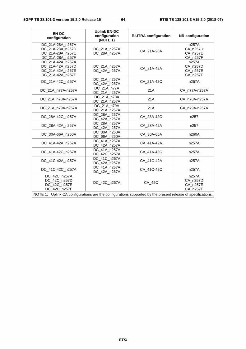


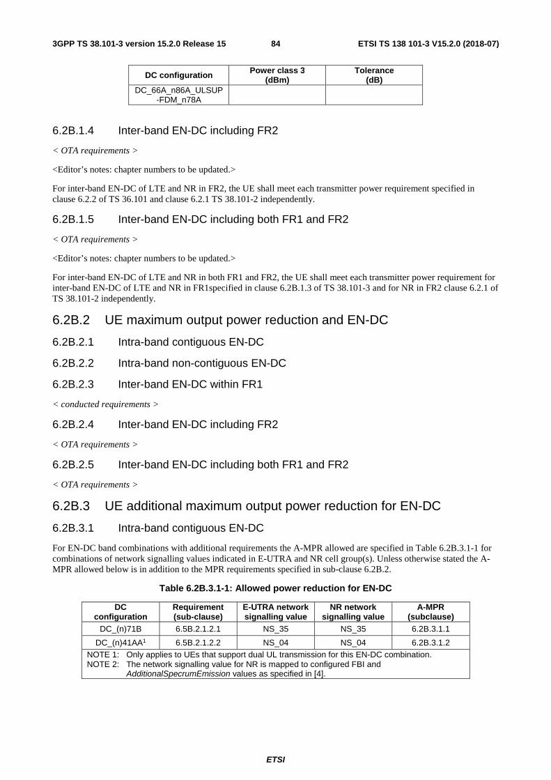


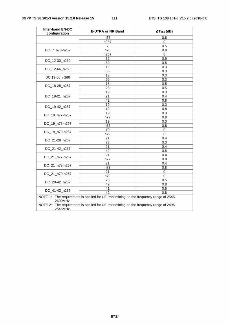


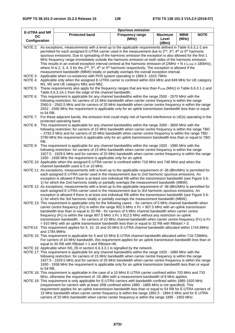

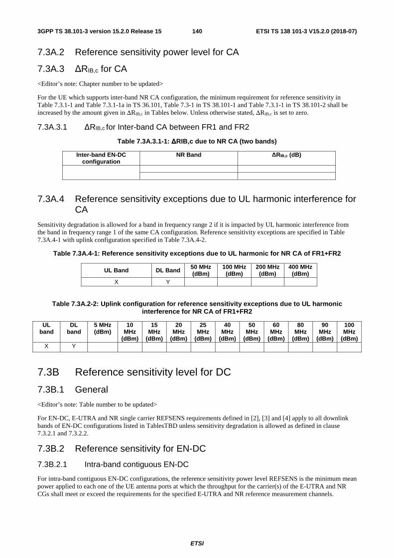


![Draft ETSI EN 301 489-50 V2.2...2002/02/02 · 4G IMT-advanced ETSI TS 137 104 [21] ETSI TS 137 141 [12] ETSI TS 137 114 [31] ETSI TS 137 145-1 [13] ETSI TS 137 145-2 [14] WMAN (OFDMA)](https://static.documents.pub/doc/80x56/60e0dd64bbf8f11159724729/draft-etsi-en-301-489-50-v22-20020202-4g-imt-advanced-etsi-ts-137-104.jpg)


![TS 128 533 - V15.2.0 - 5G; Management and orchestration ... · 3GPP TS 28.533 version 15.2.0 Release 15 7 ETSI TS 128 533 V15.2.0 (2019-10) [17] 3GPP TS 28.517: "Telecommunication](https://static.documents.pub/doc/80x56/60a24803120d833377411703/ts-128-533-v1520-5g-management-and-orchestration-3gpp-ts-28533-version.jpg)
