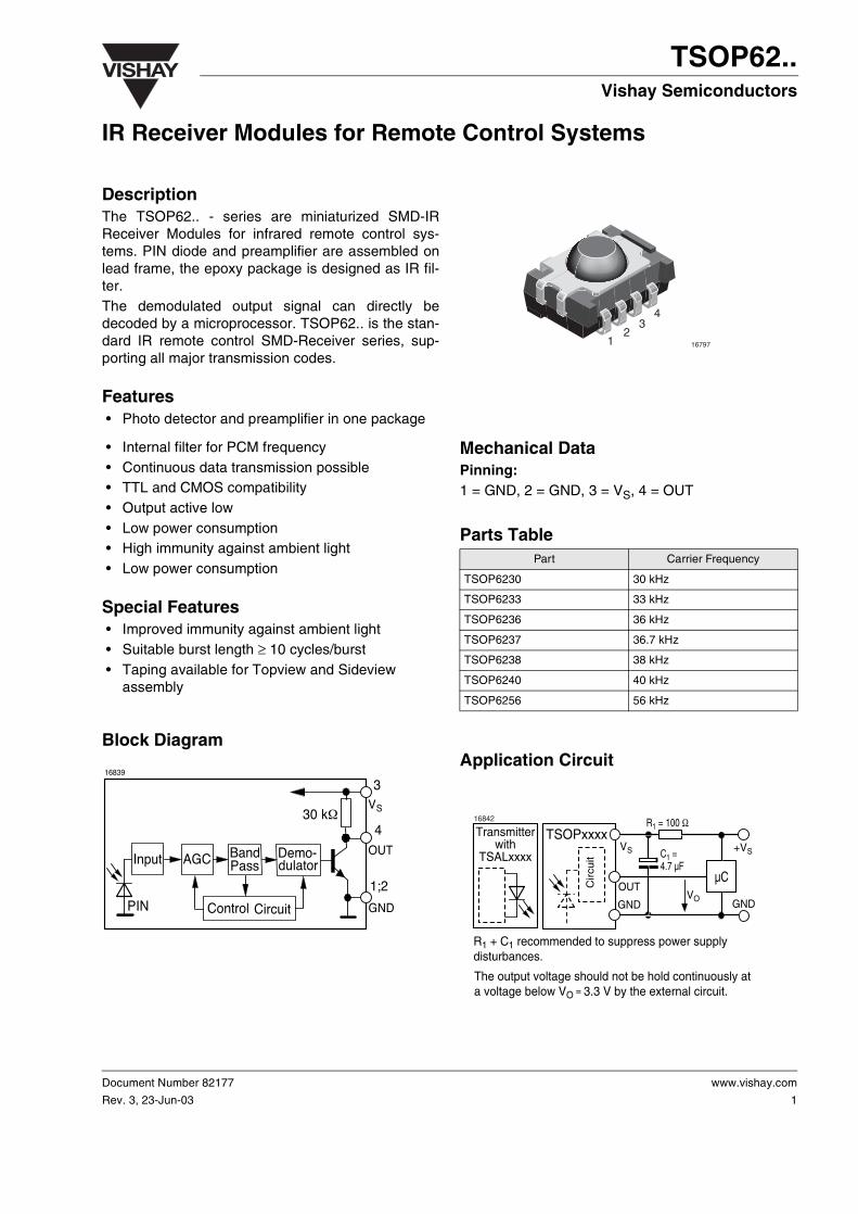
VISHAY TSOP62.. Document Number 82177 Rev. 3, 23-Jun-03 Vishay Semiconductors www.vishay.com 1 16797 1 2 3 4 IR Receiver Modules for Remote Control Systems Description The TSOP62.. - series are miniaturized SMD-IR Receiver Modules for infrared remote control sys- tems. PIN diode and preamplifier are assembled on lead frame, the epoxy package is designed as IR fil- ter. The demodulated output signal can directly be decoded by a microprocessor. TSOP62.. is the stan- dard IR remote control SMD-Receiver series, sup- porting all major transmission codes. Features • Photo detector and preamplifier in one package • Internal filter for PCM frequency • Continuous data transmission possible • TTL and CMOS compatibility • Output active low • Low power consumption • High immunity against ambient light • Low power consumption Special Features • Improved immunity against ambient light • Suitable burst length ≥ 10 cycles/burst • Taping available for Topview and Sideview assembly Mechanical Data Pinning: 1 = GND, 2 = GND, 3 = V S , 4 = OUT Parts Table Block Diagram Application Circuit Part Carrier Frequency TSOP6230 30 kHz TSOP6233 33 kHz TSOP6236 36 kHz TSOP6237 36.7 kHz TSOP6238 38 kHz TSOP6240 40 kHz TSOP6256 56 kHz 30 kΩ V S OUT Demo- GND Pass AGC Input PIN Band dulator Control Circuit 3 4 1;2 16839 C 1 = 4.7 μF TSOPxxxx OUT GND Circuit μC R 1 = 100 Ω +V S GND Transmitter with TSALxxxx V S R 1 +C 1 recommended to suppress power supply disturbances. V O The output voltage should not be hold continuously at a voltage below V O = 3.3 V by the external circuit. 16842
Transcript
VISHAY TSOP62..Vishay Semiconductors
IR Receiver Modules for Remote Control Systems
Description
167971234
The TSOP62.. - series are miniaturized SMD-IRReceiver Modules for infrared remote control sys-tems. PIN diode and preamplifier are assembled onlead frame, the epoxy package is designed as IR fil-ter.The demodulated output signal can directly bedecoded by a microprocessor. TSOP62.. is the stan-dard IR remote control SMD-Receiver series, sup-porting all major transmission codes.
Features • Photo detector and preamplifier in one package
• Internal filter for PCM frequency
• Continuous data transmission possible • TTL and CMOS compatibility • Output active low • Low power consumption • High immunity against ambient light • Low power consumption
Special Features • Improved immunity against ambient light • Suitable burst length ≥ 10 cycles/burst • Taping available for Topview and Sideview
Correlation with ambient light sources:10W/m21.4klx (Std.illum.A,T=2855K)10W/m28.2klx (Daylight,T=5900K)
Ambient, = 950 nm
E
–
Thr
esho
ld Ir
radi
ance
( m
W/m
)
e m
in2
Document Number 82177
Rev. 3, 23-Jun-03
www.vishay.com
3
VISHAYTSOP62..Vishay Semiconductors
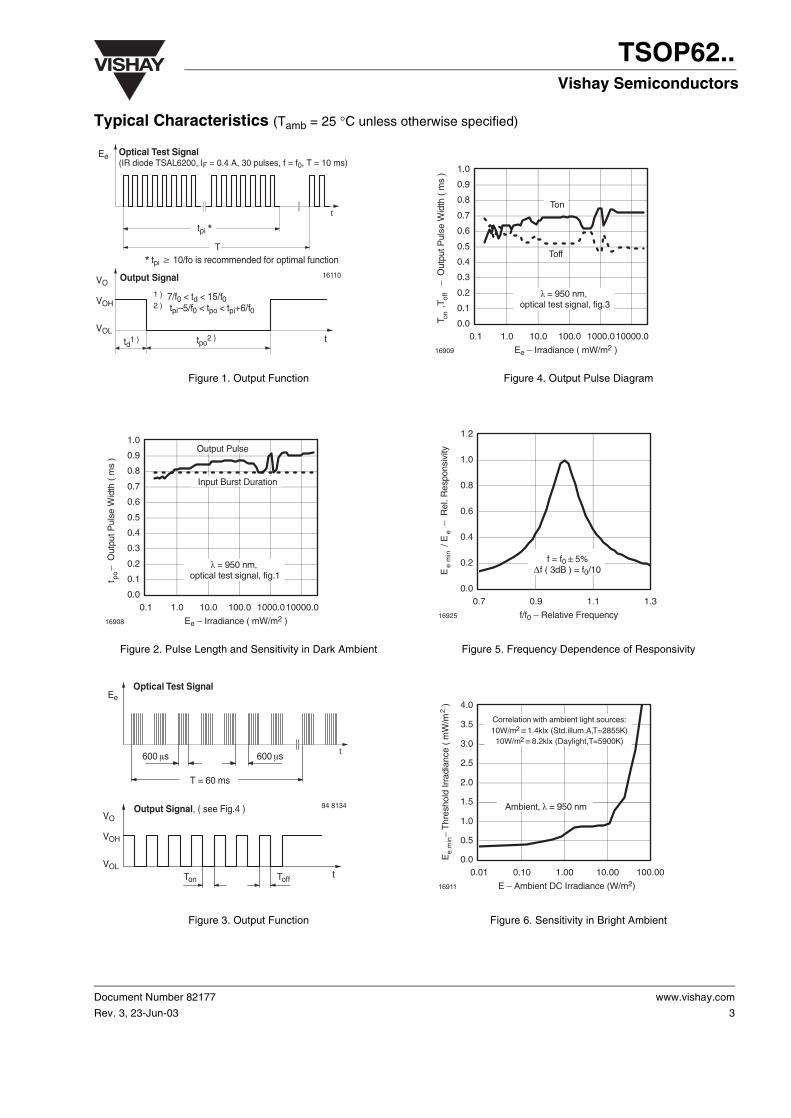
Figure 7. Sensitivity vs. Supply Voltage Disturbances
Figure 8. Sensitivity vs. Electric Field Disturbances
Figure 9. Max. Envelope Duty Cycle vs. Burstlength
0.0
0.5
1.0
1.5
2.0
0.1 1.0 10.0 100.0 1000.0
VsRMS – AC Voltage on DC Supply Voltage (mV)16912
f = fo
f = 10 kHz
E
–
Thr
esho
ld Ir
radi
ance
( m
W/m
)
e m
in2
f = 1 kHz
f = 100 Hz
E
–
Thr
esho
ld Ir
radi
ance
( m
W/m
)
0.0 0.4 0.8 1.2 1.60.0
0.4
0.8
1.2
2.0
E – Field Strength of Disturbance ( kV/m )
2.0
94 8147
1.6
e m
in2
f(E) = f0
0.0
0.1
0.2
0.3
0.4
0.5
0.6
0.7
0.8
0 20 40 60 80 100 120
Burst Length ( number of cycles / burst )16913
f = 38 kHz, Ee = 2 mW/m2
Max
. Env
elop
e D
uty
Cyc
le
Figure 10. Sensitivity vs. Ambient Temperature
Figure 11. Relative Spectral Sensitivity vs. Wavelength
Figure 12. Directivity
0.0
0.1
0.2
0.3
0.4
0.5
0.6
–30 –15 0 15 30 45 60 75 90
Tamb – Ambient Temperature ( C )16918
Sensitivity in dark ambient
E
–
Thr
esho
ld Ir
radi
ance
( m
W/m
)
e m
in2
0.0
0.2
0.4
0.6
0.8
1.0
1.2
750 850 950 1050 1150
– Wavelength ( nm )16919
S (
)
– R
elat
ive
Spe
ctra
l Sen
sitiv
ity
rel
16801
0.4 0.2 0 0.2 0.4 0.60.6
0.9
0°30°
10° 20°
40°
50°
60°
70°
80°
1.0
0.8
0.7
drel - Relative Transmission Distance
www.vishay.com
4
Document Number 82177
Rev. 3, 23-Jun-03
VISHAY TSOP62..Vishay Semiconductors
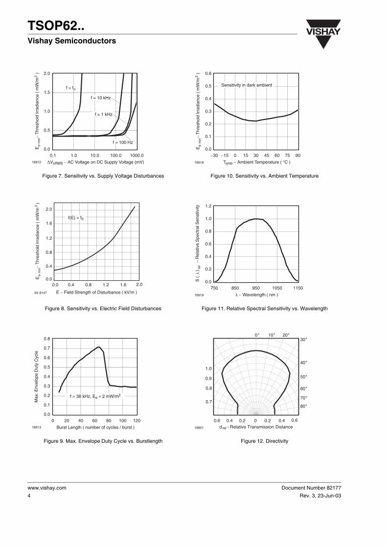
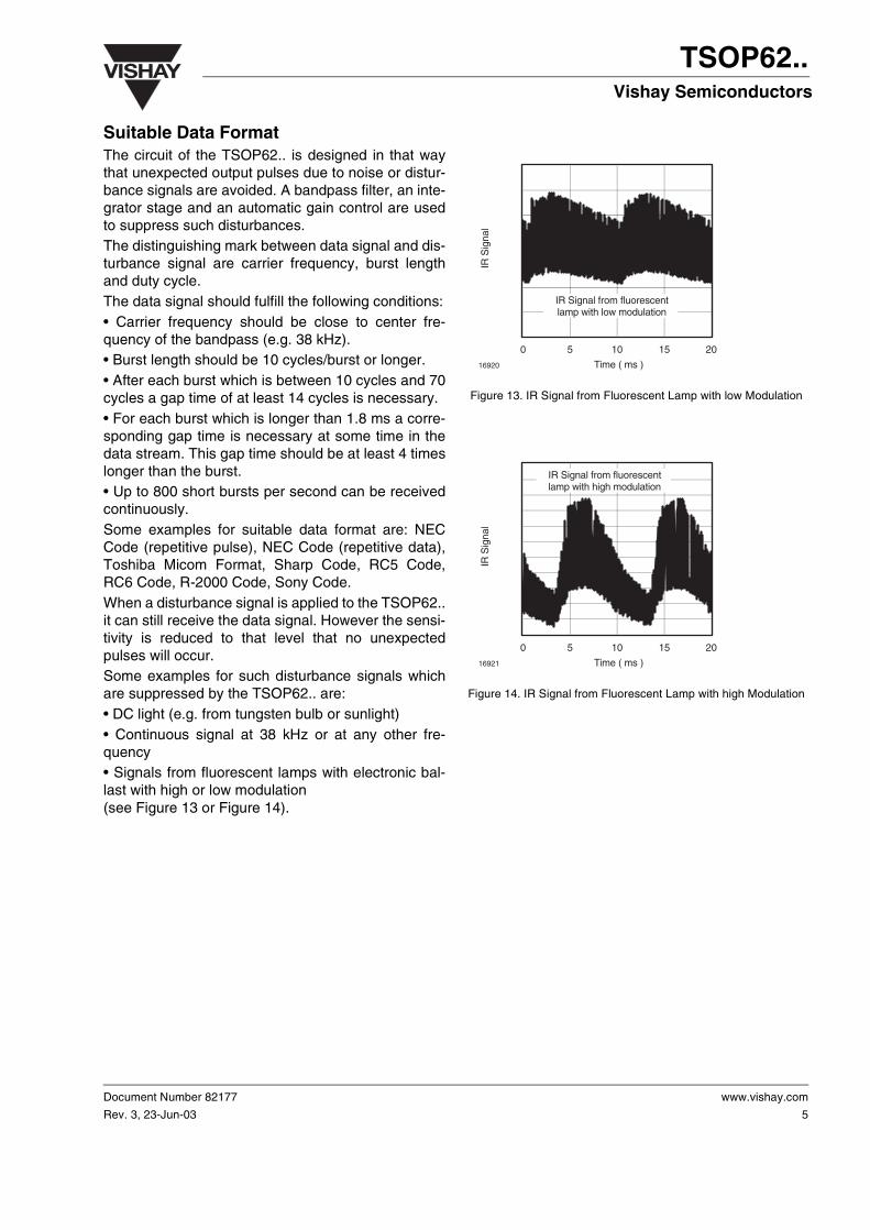
Suitable Data FormatThe circuit of the TSOP62.. is designed in that waythat unexpected output pulses due to noise or distur-bance signals are avoided. A bandpass filter, an inte-grator stage and an automatic gain control are usedto suppress such disturbances.The distinguishing mark between data signal and dis-turbance signal are carrier frequency, burst lengthand duty cycle.The data signal should fulfill the following conditions:• Carrier frequency should be close to center fre-quency of the bandpass (e.g. 38 kHz).• Burst length should be 10 cycles/burst or longer.• After each burst which is between 10 cycles and 70cycles a gap time of at least 14 cycles is necessary.• For each burst which is longer than 1.8 ms a corre-sponding gap time is necessary at some time in thedata stream. This gap time should be at least 4 timeslonger than the burst.• Up to 800 short bursts per second can be receivedcontinuously.Some examples for suitable data format are: NECCode (repetitive pulse), NEC Code (repetitive data),Toshiba Micom Format, Sharp Code, RC5 Code,RC6 Code, R-2000 Code, Sony Code.When a disturbance signal is applied to the TSOP62..it can still receive the data signal. However the sensi-tivity is reduced to that level that no unexpectedpulses will occur.Some examples for such disturbance signals whichare suppressed by the TSOP62.. are:• DC light (e.g. from tungsten bulb or sunlight)• Continuous signal at 38 kHz or at any other fre-quency• Signals from fluorescent lamps with electronic bal-last with high or low modulation (see Figure 13 or Figure 14).
Figure 13. IR Signal from Fluorescent Lamp with low Modulation
Figure 14. IR Signal from Fluorescent Lamp with high Modulation
0 5 10 15 20
Time ( ms )16920
IR S
igna
l
IR Signal from fluorescentlamp with low modulation
0 5 10 15 20
Time ( ms )16921
IR S
igna
lIR Signal from fluorescentlamp with high modulation
Document Number 82177
Rev. 3, 23-Jun-03
www.vishay.com
5
VISHAYTSOP62..Vishay Semiconductors
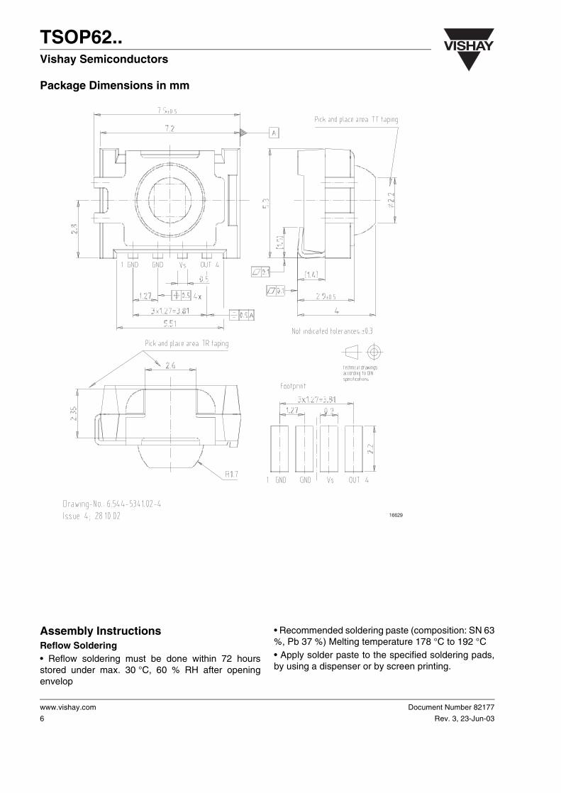
Package Dimensions in mm
Assembly InstructionsReflow Soldering• Reflow soldering must be done within 72 hoursstored under max. 30 °C, 60 % RH after openingenvelop
• Recommended soldering paste (composition: SN 63%, Pb 37 %) Melting temperature 178 °C to 192 °C• Apply solder paste to the specified soldering pads,by using a dispenser or by screen printing.
16629
www.vishay.com
6
Document Number 82177
Rev. 3, 23-Jun-03
VISHAY TSOP62..Vishay Semiconductors
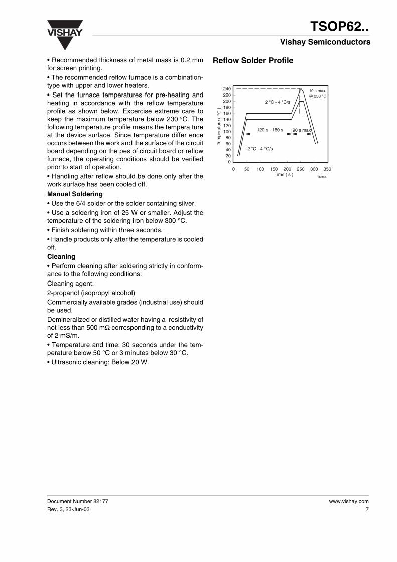
• Recommended thickness of metal mask is 0.2 mmfor screen printing.• The recommended reflow furnace is a combination-type with upper and lower heaters.• Set the furnace temperatures for pre-heating andheating in accordance with the reflow temperatureprofile as shown below. Excercise extreme care tokeep the maximum temperature below 230 °C. Thefollowing temperature profile means the tempera tureat the device surface. Since temperature differ enceoccurs between the work and the surface of the circuitboard depending on the pes of circuit board or reflowfurnace, the operating conditions should be verifiedprior to start of operation.• Handling after reflow should be done only after thework surface has been cooled off.Manual Soldering• Use the 6/4 solder or the solder containing silver.• Use a soldering iron of 25 W or smaller. Adjust thetemperature of the soldering iron below 300 °C.• Finish soldering within three seconds.• Handle products only after the temperature is cooledoff.Cleaning• Perform cleaning after soldering strictly in conform-ance to the following conditions:Cleaning agent:2-propanol (isopropyl alcohol)Commercially available grades (industrial use) shouldbe used.Demineralized or distilled water having a resistivity ofnot less than 500 mΩ corresponding to a conductivityof 2 mS/m.• Temperature and time: 30 seconds under the tem-perature below 50 °C or 3 minutes below 30 °C.• Ultrasonic cleaning: Below 20 W.
Reflow Solder Profile
10 s max.@ 230 C
90 s max
020406080
100120140160180200220240
0 50 100 150 200 250 300 350Time ( s )
Tem
pera
ture
(
C )
16944
2 C - 4 C/s
120 s - 180 s
2 C - 4 C/s
Document Number 82177
Rev. 3, 23-Jun-03
www.vishay.com
7
VISHAYTSOP62..Vishay Semiconductors
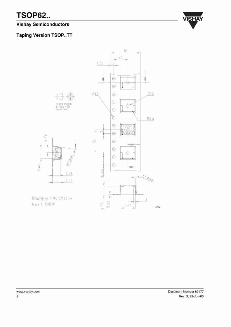
Taping Version TSOP..TT
16584
www.vishay.com
8
Document Number 82177
Rev. 3, 23-Jun-03
VISHAY TSOP62..Vishay Semiconductors
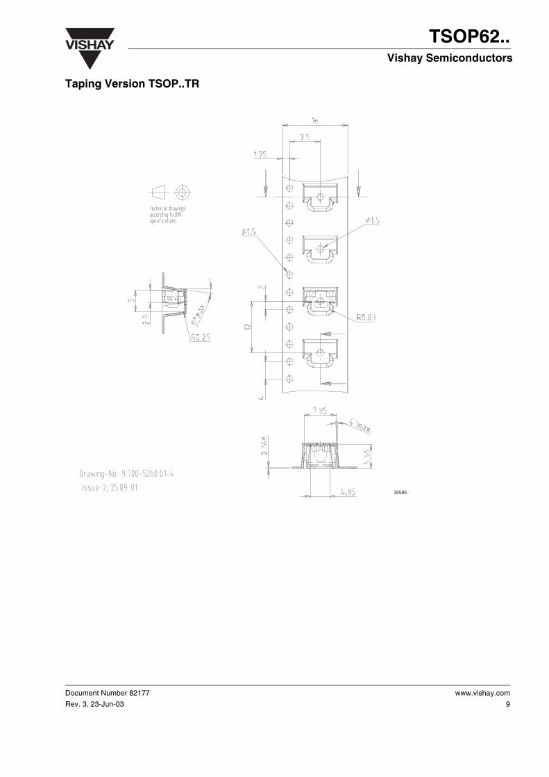
Taping Version TSOP..TR
16585
Document Number 82177
Rev. 3, 23-Jun-03
www.vishay.com
9
VISHAYTSOP62..Vishay Semiconductors
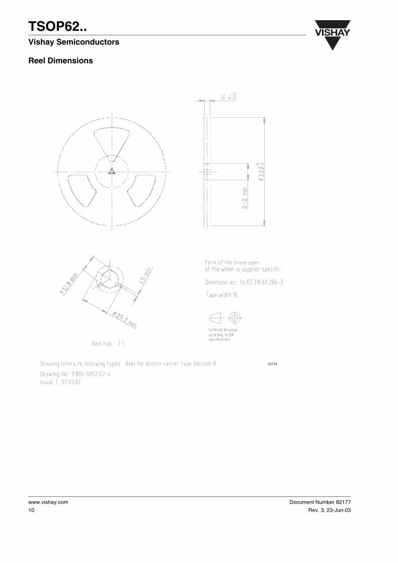
Reel Dimensions
16734
www.vishay.com
10
Document Number 82177
Rev. 3, 23-Jun-03
VISHAY TSOP62..Vishay Semiconductors
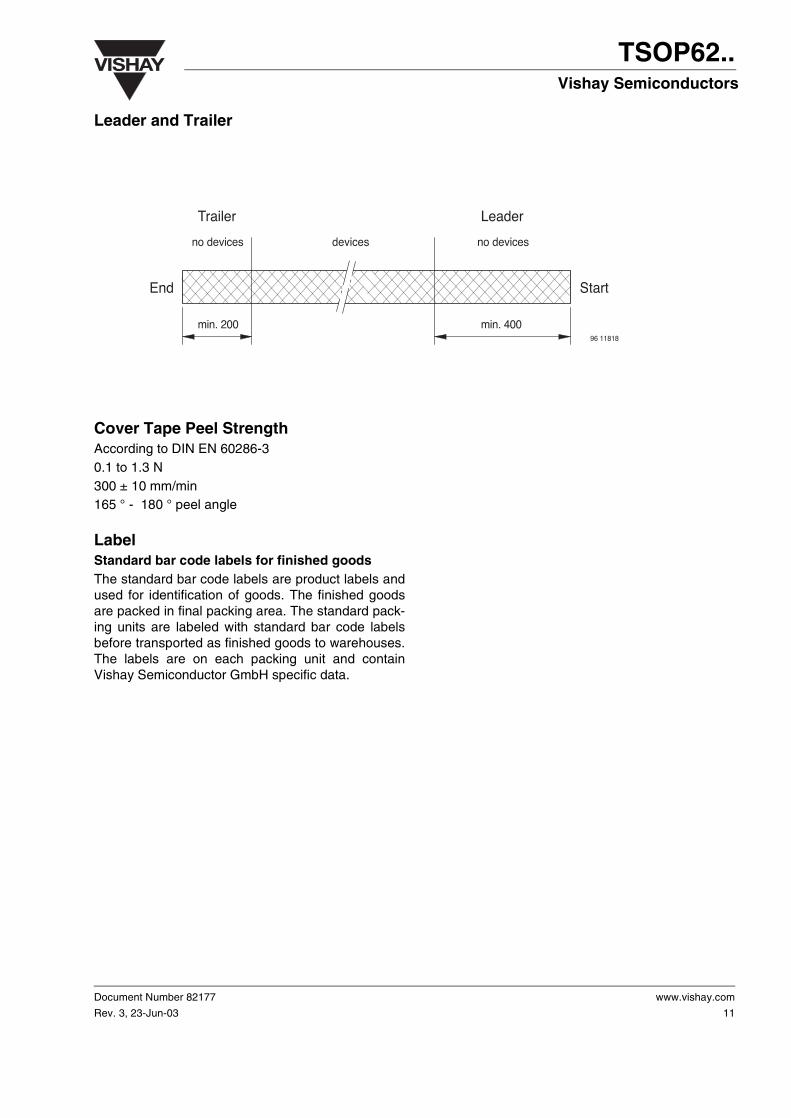
Leader and Trailer
Cover Tape Peel StrengthAccording to DIN EN 60286-30.1 to 1.3 N300 ± 10 mm/min165 ° - 180 ° peel angle
LabelStandard bar code labels for finished goodsThe standard bar code labels are product labels andused for identification of goods. The finished goodsare packed in final packing area. The standard pack-ing units are labeled with standard bar code labelsbefore transported as finished goods to warehouses.The labels are on each packing unit and containVishay Semiconductor GmbH specific data.
Trailer Leader
no devices no devices
min. 200 min. 400
StartEnd
devices
96 11818
Document Number 82177
Rev. 3, 23-Jun-03
www.vishay.com
11
VISHAYTSOP62..Vishay Semiconductors
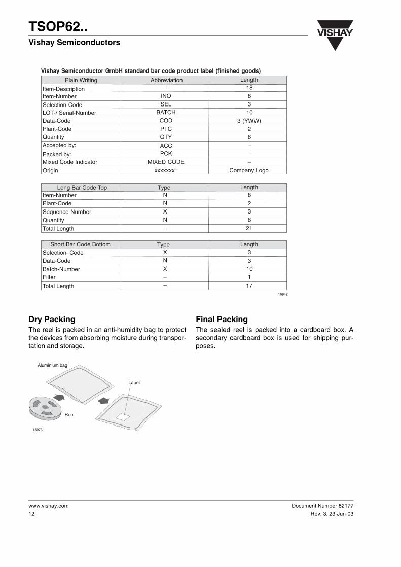
Dry PackingThe reel is packed in an anti-humidity bag to protectthe devices from absorbing moisture during transpor-tation and storage.
Final PackingThe sealed reel is packed into a cardboard box. Asecondary cardboard box is used for shipping pur-poses.
Vishay Semiconductor GmbH standard bar code product label (finished goods)
Aluminium bag
Label
Reel
15973
www.vishay.com
12
Document Number 82177
Rev. 3, 23-Jun-03
VISHAY TSOP62..Vishay Semiconductors
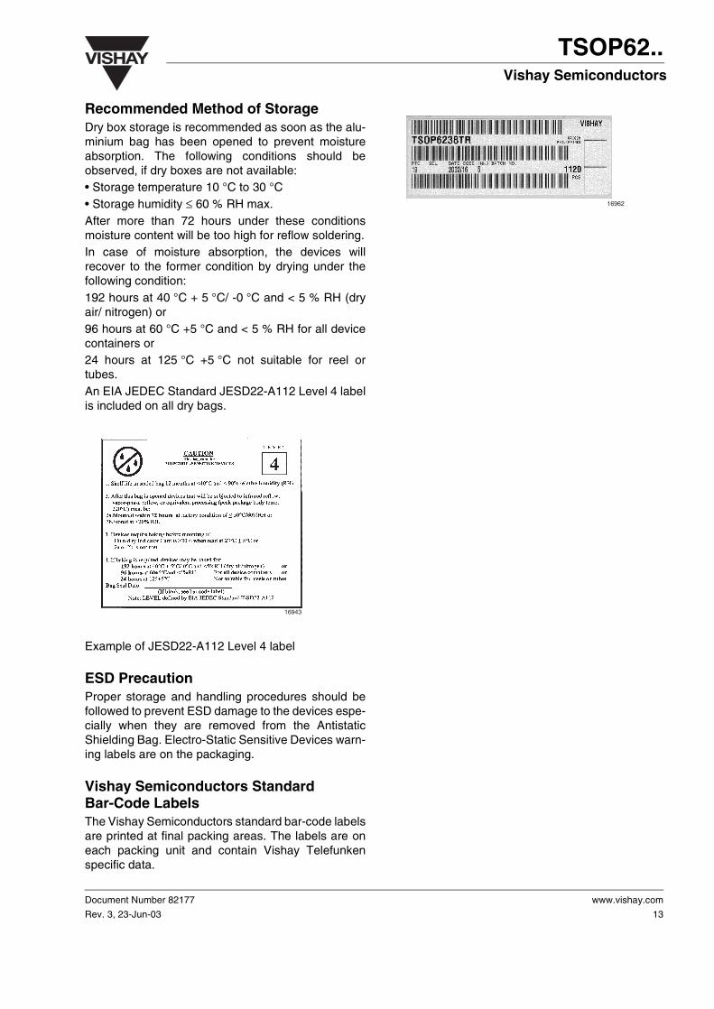
Recommended Method of StorageDry box storage is recommended as soon as the alu-minium bag has been opened to prevent moistureabsorption. The following conditions should beobserved, if dry boxes are not available:• Storage temperature 10 °C to 30 °C• Storage humidity ≤ 60 % RH max.After more than 72 hours under these conditionsmoisture content will be too high for reflow soldering.In case of moisture absorption, the devices willrecover to the former condition by drying under thefollowing condition:192 hours at 40 °C + 5 °C/ -0 °C and < 5 % RH (dryair/ nitrogen) or96 hours at 60 °C +5 °C and < 5 % RH for all devicecontainers or24 hours at 125 °C +5 °C not suitable for reel ortubes.An EIA JEDEC Standard JESD22-A112 Level 4 labelis included on all dry bags.
Example of JESD22-A112 Level 4 label
ESD PrecautionProper storage and handling procedures should befollowed to prevent ESD damage to the devices espe-cially when they are removed from the AntistaticShielding Bag. Electro-Static Sensitive Devices warn-ing labels are on the packaging.
Vishay Semiconductors StandardBar-Code LabelsThe Vishay Semiconductors standard bar-code labelsare printed at final packing areas. The labels are oneach packing unit and contain Vishay Telefunkenspecific data.
16943
16962
Document Number 82177
Rev. 3, 23-Jun-03
www.vishay.com
13
VISHAYTSOP62..Vishay Semiconductors
Ozone Depleting Substances Policy Statement
It is the policy of Vishay Semiconductor GmbH to
1. Meet all present and future national and international statutory requirements.
2. Regularly and continuously improve the performance of our products, processes, distribution and operatingsystems with respect to their impact on the health and safety of our employees and the public, as well as their impact on the environment.
It is particular concern to control or eliminate releases of those substances into the atmosphere which are known as ozone depleting substances (ODSs).
The Montreal Protocol (1987) and its London Amendments (1990) intend to severely restrict the use of ODSs and forbid their use within the next ten years. Various national and international initiatives are pressing for an earlier ban on these substances.
Vishay Semiconductor GmbH has been able to use its policy of continuous improvements to eliminate the use of ODSs listed in the following documents.
1. Annex A, B and list of transitional substances of the Montreal Protocol and the London Amendments respectively
2. Class I and II ozone depleting substances in the Clean Air Act Amendments of 1990 by the Environmental Protection Agency (EPA) in the USA
3. Council Decision 88/540/EEC and 91/690/EEC Annex A, B and C (transitional substances) respectively.
Vishay Semiconductor GmbH can certify that our semiconductors are not manufactured with ozone depleting substances and do not contain such substances.
We reserve the right to make changes to improve technical design and may do so without further notice.
Parameters can vary in different applications. All operating parameters must be validated for each customer application by the customer. Should the buyer use Vishay Semiconductors products for any unintended or unauthorized application, the buyer shall indemnify Vishay Semiconductors against all
claims, costs, damages, and expenses, arising out of, directly or indirectly, any claim of personal damage, injury or death associated with such unintended or unauthorized use.


![C22 Preamplifier Complete User Manual - Analog Metricanalogmetric.com/download/C22 Preamplifier Complete User Manual.pdf · [C22 VACUUM TUBE PREAMPLIFIER COMPLETE USER MANUAL ] ...](https://static.documents.pub/doc/80x56/5ad3f8607f8b9abd6c8eae98/c22-preamplifier-complete-user-manual-analog-preamplifier-complete-user-manualpdfc22.jpg)