. INTRODUCTIONhe field of surface plasmon polaritons (SPPs) [1] haseen rapidly developing over the past couple of decades.ne of the active plasmonic-related research topics is theaveguiding characteristics of multilayered plasmonic
tructures [2]. A basic example for such a structure is thatf a thin metal film sandwiched between two dielectricinsulating) media [insulator/metal/insulator (IMI)]. For ahin enough film, the SPP modes guided by the twoielectric-metal interfaces are coupled through the metal,hus creating supermodes that exhibit a dispersion vary-ng with the metal thickness. A variant of the IMI struc-ure that has been studied recently is a doubly corrugatedetallic layer which was analyzed for sinusoidal [3,4] and
ectangular [5,6] gratings, with possible applications for aandgap plasmonic laser and optical filters. A more com-lex multilayered configuration is the double metal platetructure, comprising an insulator/metal/insulator/metal/nsulator (IMIMI) interface. The dispersion equations andhe waveguiding characteristics of this configuration haveeen studied by [7–9]. This structure was recently appliedor the calculation of the optical forces between the metal-ic plates [10]. In this paper, we study a symmetric one-imensional IMIMI structure, of which each of the twoetallic layers is periodically corrugated. We analyze this
onfiguration and show that the relative shift between theorrugated interfaces controls the interaction between theodes supported by the structure. Furthermore, we dem-
nstrate that the control of these interactions enablesunable filtering properties of both the reflection and theransmission spectra. The computer simulations used forhis study are based on the rigorous coupled wave analy-
is (RCWA) method, also known as the Fourier modalethod. We apply the factorization rules that lead to
aster convergence for transverse magnetic (TM) polariza-ion [11–14]. The paper is structured as follows. In Sec-ion 2, the modes supported by the structure are de-cribed and classified into groups. In Section 3, it isemonstrated how the interactions between the plas-onic and the photonic modes form an effective “absorp-
ion gap,” both under normal and oblique incidences. Inection 4, we show how the shift in absorbance lines cane utilized to obtain tunable filtering properties of the re-ection and transmission spectra. Furthermore, we showto our knowledge, for the first time) how the poor trans-ission can be enhanced by introducing a large refractive
ndex contrast between the substrate/superstrate and their gap separating the metallic plates.
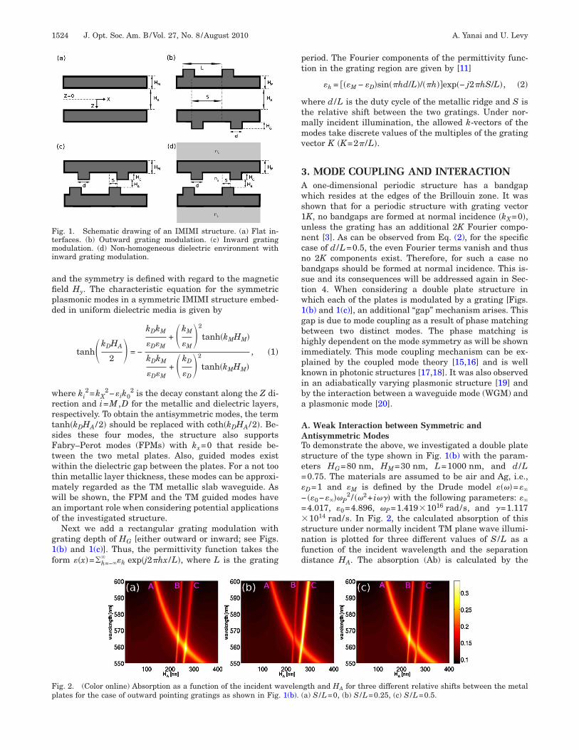
. MODES OF AN IMIMI STRUCTUREigure 1(a) shows a flat double plate structure, withetal layer thickness HM and dielectric gap between the
lates, HA. As previously analyzed [7–10], a symmetricouble metal plate supports four plasmonic modes. Theseodes can be classified as two long-range surface plas-on polariton (LRSPP) modes, which can be either sym-etric or antisymmetric with respect to each other (de-ned as LRS and LRA), and two short-range surfacelasmon polariton (SRSPP) modes, which can also be ei-her symmetric or antisymmetric with respect to eachther (SRS and SRA).
Throughout this paper the plane of symmetry is as-umed to be in the middle of the dielectric gap H �z=0�
A
010 Optical Society of America
afipd
wrrtsFtwtmwao
g1f
pt
wtmmv
3Aws1uncnbstw1gbhipkiba
AATse=�
−=�snfd
Ftmi
Fp
1524 J. Opt. Soc. Am. B/Vol. 27, No. 8 /August 2010 A. Yanai and U. Levy
nd the symmetry is defined with regard to the magneticeld Hy. The characteristic equation for the symmetriclasmonic modes in a symmetric IMIMI structure embed-ed in uniform dielectric media is given by
tanh�kDHA
2 � = −
kDkM
�D�M+ �kM
�M�2
tanh�kMHM�
kDkM
�D�M+ �kD
�D�2
tanh�kMHM�
, �1�
here ki2=kX
2−�ik02 is the decay constant along the Z di-
ection and i=M ,D for the metallic and dielectric layers,espectively. To obtain the antisymmetric modes, the termanh�kDHA /2� should be replaced with coth�kDHA /2�. Be-ides these four modes, the structure also supportsabry–Perot modes (FPMs) with kx=0 that reside be-
ween the two metal plates. Also, guided modes existithin the dielectric gap between the plates. For a not too
hin metallic layer thickness, these modes can be approxi-ately regarded as the TM metallic slab waveguide. Asill be shown, the FPM and the TM guided modes haven important role when considering potential applicationsf the investigated structure.
Next we add a rectangular grating modulation withrating depth of HG [either outward or inward; see Figs.(b) and 1(c)]. Thus, the permittivity function takes theorm ��x�=�h=−�
� �h exp�j2�hx /L�, where L is the grating
ig. 1. Schematic drawing of an IMIMI structure. (a) Flat in-erfaces. (b) Outward grating modulation. (c) Inward gratingodulation. (d) Non-homogeneous dielectric environment with
nward grating modulation.
ig. 2. (Color online) Absorption as a function of the incident wlates for the case of outward pointing gratings as shown in Fig
eriod. The Fourier components of the permittivity func-ion in the grating region are given by [11]
here d /L is the duty cycle of the metallic ridge and S ishe relative shift between the two gratings. Under nor-ally incident illumination, the allowed k-vectors of theodes take discrete values of the multiples of the grating
ector K �K=2� /L�.
. MODE COUPLING AND INTERACTIONone-dimensional periodic structure has a bandgap
hich resides at the edges of the Brillouin zone. It washown that for a periodic structure with grating vectorK, no bandgaps are formed at normal incidence �kX=0�,nless the grating has an additional 2K Fourier compo-ent [3]. As can be observed from Eq. (2), for the specificase of d /L=0.5, the even Fourier terms vanish and thuso 2K components exist. Therefore, for such a case noandgaps should be formed at normal incidence. This is-ue and its consequences will be addressed again in Sec-ion 4. When considering a double plate structure inhich each of the plates is modulated by a grating [Figs.(b) and 1(c)], an additional “gap” mechanism arises. Thisap is due to mode coupling as a result of phase matchingetween two distinct modes. The phase matching isighly dependent on the mode symmetry as will be shown
mmediately. This mode coupling mechanism can be ex-lained by the coupled mode theory [15,16] and is wellnown in photonic structures [17,18]. It was also observedn an adiabatically varying plasmonic structure [19] andy the interaction between a waveguide mode (WGM) andplasmonic mode [20].
. Weak Interaction between Symmetric andntisymmetric Modeso demonstrate the above, we investigated a double platetructure of the type shown in Fig. 1(b) with the param-ters HG=80 nm, HM=30 nm, L=1000 nm, and d /L0.75. The materials are assumed to be air and Ag, i.e.,D=1 and �M is defined by the Drude model ����=��
��0−����P2 / ��2+ i��� with the following parameters: ��
4.017, �0=4.896, �P=1.419�1016 rad/s, and �=1.1171014 rad/s. In Fig. 2, the calculated absorption of this
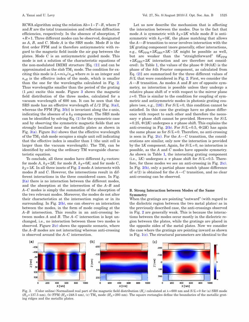
tructure under normally incident TM plane wave illumi-ation is plotted for three different values of S /L as aunction of the incident wavelength and the separationistance HA. The absorption (Ab) is calculated by the
gth and HA for three different relative shifts between the metal(a) S /L=0, (b) S /L=0.25, (c) S /L=0.5.
avelen. 1(b).
Rae+afigpmtacntT�fivSwicasFotlit
fkmf2aAttsbAtcoti
tmst2eb+epESAmrzmpses=atiebpA(fIoa
BSWttitgtti
F�i
A. Yanai and U. Levy Vol. 27, No. 8 /August 2010 /J. Opt. Soc. Am. B 1525
CWA algorithm using the relation Ab=1−T−R, where Tnd R are the total transmission and reflection diffractionfficiencies, respectively. In the absence of absorption, TR=1. Three different modes can be observed, designateds A, B, and C. Mode A is the SRS mode. Mode B is therst order FPM and is therefore antisymmetric with re-ard to the magnetic field inside the air gap between thelates. Mode C is an antisymmetric guided mode. Thisode is not a solution of the characteristic equations of
he non-modulated IMIMI structure [Eq. (1)] and can bepproximated as the slab TM1 mode. The condition for ex-iting this mode is L=m�0 /neff where m is an integer andeff is the effective index of the mode, which is smallerhan the one for the wavelengths calculated in Fig. 2.hus wavelengths smaller than the period of the grating
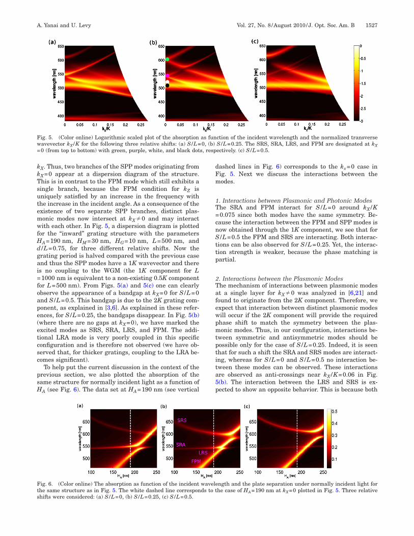
1 �m� excite this mode. Figure 3 shows the magneticeld distribution of the three modes, calculated for aacuum wavelength of 600 nm. It can be seen that theRS mode has an effective wavelength of L /2 [Fig. 3(a)],hereas the FPM [Fig. 3(b)] is invariant along the x-axis,
ndicating the absence of a kX component. The SRS modean be identified by solving Eq. (1) for the symmetric casend by observing the symmetric magnetic fields that aretrongly localized near the metallic plates as shown inig. 3(a). Figure 3(c) shows that the effective wavelengthf the TM1 slab mode occupies a single unit cell indicatinghat the effective index is smaller than 1 (the unit cell isarger than the vacuum wavelength). The TM1 can bedentified by solving the ordinary TM waveguide charac-eristic equation.
To conclude, all three modes have different kX-vectors:or mode A, kX=2K; for mode B, kX=0K; and for mode C,X=1K. In all three insets of Fig. 2 mode A intersects withodes B and C. However, the intersections result in dif-
erent interactions in the three considered cases. In Fig.(a) there is no interaction between the different modes,nd the absorption at the intersection of the A–B and–C modes is simply the summation of the absorption of
he two relevant modes. Moreover, the modes do not alterheir characteristics at the intersection region or in itsurrounding. In Fig. 2(b), one can observe an interactionetween the modes, in the form of mode coupling at the–B intersection. This results in an anti-crossing be-
ween modes A and B. The A–C intersection is kept un-hanged, i.e., no interaction between these two modes isbserved. Figure 2(c) shows the opposite scenario, wherehe A–B modes are not interacting whereas anti-crossings observed around the A–C intersection.
ig. 3. (Color online) Normalized real part of the magnetic fieldHA=137.5 nm�, (b) FPM �HA=248.5 nm�, (c) TM1 mode �HA=293ng ridges and the metallic plates.
Let us now describe the mechanism that is affectinghe interaction between the modes. Due to the fact thatode A is symmetric with kX=2K while mode B is anti-
ymmetric with kX=0K, the phase matching that allowshe A↔B transition to occur involves interaction with theK grating component (more generally, other interactions,.g., 0KFPM+2KSRS=3K−1K might be possible as well,ut are weaker than the “straightforward” 0KFPM2KSRS=2K interaction and are therefore not consid-red). In Table 1, the values of the phase [�hK� is thehase of the hth Fourier component, as calculated fromq. (2)] are summarized for the three different values of/L that were considered in Fig. 2. First, we consider the↔B transition. As modes A and B are of opposite sym-etry, no interaction is possible unless they undergo a
elative phase shift of � with respect to the mirror plane=0. This is similar to the condition for coupling of sym-etric and antisymmetric modes in photonic grating cou-
lers (see, e.g., [18]). For S /L=0, this condition cannot beatisfied. In this case the gratings have no phase differ-nce with respect to each other and therefore the neces-ary � phase shift cannot be provided. However, for S /L0.25, �2K� undergoes a � phase shift. This explains thenti-crossing in Fig. 2(b). For S /L=0.5, �2K� has againhe same phase as for S /L=0. Therefore, no anti-crossings seen in Fig. 2(c). For the A↔C transition, the consid-rations are similar, only now the interaction is providedy the 1K component. Again, for S /L=0, no interaction isossible, as the A and C modes have opposite symmetry.s shown in Table 1, the interacting grating component
i.e., 1K) undergoes a � phase shift for S /L=0.5. There-ore, for these modes we see an anti-crossing in Fig. 2(c).n Fig. 2(b), only a partial phase match (phase differencef � /2) is obtained for the A↔C transition, and no clearnti-crossing can be observed.
. Strong Interaction between Modes of the Sameymmetryhen the gratings are pointing “outward” (with regard to
he dielectric region between the two metal plates) as inhe previously described case, the anti-crossings observedn Fig. 2 are generally weak. This is because the interac-ions between the modes occur mostly in the dielectric re-ion between the plates, while the gratings are placed inhe opposite sides of the metal plates. Now we considerhe case where the gratings are pointing inward as shownn Fig. 1(c). The structural parameters are identical to the
ution �Hy� calculated at �=600 nm and S /L=0 for (a) SRS modehe square rectangles define the boundaries of the metallic grat-
distribnm�. T
ptetfcapTiatFnltsrpcmstb2
tpsobttAim[4tttst
CWdpps
FpsS(
1526 J. Opt. Soc. Am. B/Vol. 27, No. 8 /August 2010 A. Yanai and U. Levy
reviously discussed structure (Subsection 3.A) excepthat HG=30 nm, with the gratings extending into the di-lectric gap between the plates. The absorption curves ofhis structure are plotted in Figs. 4(a)–4(c), for three dif-erent values of S /L. Figure 4(d) shows schematically theurves of the original unperturbed modes as they wouldpproximately exist without inter-modal interaction, su-erimposed on the S /L=0 case [also shown in Fig. 4(a)].hese unperturbed modes are marked by the green (des-
gnated as AA and AS), blue (BA and BS), and white (CAnd CS) lines. As in the previous simpler case, we havehree modes A, B, and C which are the SRSPP modes,PM, and WGMs, respectively, where the subscripts de-ote the symmetry. In this example we are considering a
arger domain both in wavelength and in separation be-ween the plates. As a result, we can now observe bothymmetries of the three modes. In Fig. 4(d), AA and ASepresent the SRA and SRS modes, respectively. As ex-ected, these two modes can be seen to have the sameharacteristics in the limit of HA→� as the two IMIodes have no interaction. BA and BS are the first and
econd order FPMs, respectively, having opposite symme-ry. CA and CS are WGMs (TM1 and TM2, respectively). Asefore, the K-vectors of the SRSPP, FPM, and WGM areK, 0K, and 1K, respectively. In Fig. 4(a), we can observe
Table 1. Phases of the Three Modes and Phase MatRelative
S /L �0K� �1K�
0 0 00.25 0 � /20.5 0 �
aPM stands for phase matching.
ig. 4. (Color online) Absorption as a function of the incident wlates for the case of inward pointing gratings as shown in Fig. 1upported modes as they would approximately appear with no in/L=0 scenario that is also shown in Fig. 3(a). The green, blue, a
both symmetric and antisymmetric).
he interactions AA↔BA, AS↔BS, and AA↔CA as ex-ected since only interactions between modes of the sameymmetry are allowed. The AS↔CS interaction cannot bebserved. The absence of this transition may be explainedy the strong AS↔BS transition, masking other interac-ions. In Fig. 4(b) the 2K interactions of opposite symme-ry are allowed. Therefore we see the AS↔BA andA↔BS interactions. We also identify interactions involv-
ng the 1K component between modes of the same sym-etry, because the 1K component is partially matched
i.e., AA↔CA and also AS↔CS which in contrary to Fig.(a) is now visible as it is not masked by the AS↔BS in-eraction which is now forbidden]. In Fig. 4(c) we see in-eractions between modes of opposite symmetry due tohe 1K component (AS↔CA and AA↔CS) and continue toee interactions between modes of the same symmetryhat are due to the 2K component (AA↔BA and AS↔BS).
. Mode Hybridization Under Oblique Incidencee now consider the effect of changing the angle of inci-
ence. For small oblique incident angles (incident TMlane wave is tilted in the X-Z plane), the above discussedlasmonic modes will have two possible frequencies whicholve the SPP characteristic equation [Eq. (1)] for a given
between the Different Modes for Three Values ofng Shift
A↔B �2K↔0K� A↔C �2K↔1K�
No PMa No PMPM Partial PM
No PM PM
gth and HA for three different relative shifts between the metalS /L=0, (b) S /L=0.25, (c) S /L=0.5. (d) Schematic drawing of theodal interaction. The schematic curves are superimposed on theite lines represent SRSPP modes, FPM, and WGM, respectively
chingGrati
�2K�
0�
0
avelen(c). (a)ter-mnd wh
kkTsutemwfHdgai=foape(etcsc
psH
dFm
1T=cnSttp
2Tafewpmtptita5p
Fw=
Fts
A. Yanai and U. Levy Vol. 27, No. 8 /August 2010 /J. Opt. Soc. Am. B 1527
X. Thus, two branches of the SPP modes originating fromX=0 appear at a dispersion diagram of the structure.his is in contrast to the FPM mode which still exhibits aingle branch, because the FPM condition for kZ isniquely satisfied by an increase in the frequency withhe increase in the incident angle. As a consequence of thexistence of two separate SPP branches, distinct plas-onic modes now intersect at kX�0 and may interactith each other. In Fig. 5, a dispersion diagram is plotted
or the “inward” grating structure with the parametersA=190 nm, HM=30 nm, HG=10 nm, L=500 nm, and/L=0.75, for three different relative shifts. Now therating period is halved compared with the previous casend thus the SPP modes have a 1K wavevector and theres no coupling to the WGM (the 1K component for L1000 nm is equivalent to a non-existing 0.5K component
or L=500 nm). From Figs. 5(a) and 5(c) one can clearlybserve the appearance of a bandgap at kX=0 for S /L=0nd S /L=0.5. This bandgap is due to the 2K grating com-onent, as explained in [3,6]. As explained in these refer-nces, for S /L=0.25, the bandgaps disappear. In Fig. 5(b)where there are no gaps at kX=0), we have marked thexcited modes as SRS, SRA, LRS, and FPM. The addi-ional LRA mode is very poorly coupled in this specificonfiguration and is therefore not observed (we have ob-erved that, for thicker gratings, coupling to the LRA be-omes significant).
To help put the current discussion in the context of therevious section, we also plotted the absorption of theame structure for normally incident light as a function ofA (see Fig. 6). The data set at HA=190 nm (see vertical
ig. 5. (Color online) Logarithmic scaled plot of the absorptionavevector kX /K for the following three relative shifts: (a) S /L=0 (from top to bottom) with green, purple, white, and black dot
ig. 6. (Color online) The absorption as function of the incidenthe same structure as in Fig. 5. The white dashed line corresponhifts were considered: (a) S /L=0, (b) S /L=0.25, (c) S /L=0.5.
ashed lines in Fig. 6) corresponds to the kx=0 case inig. 5. Next we discuss the interactions between theodes.
. Interactions between Plasmonic and Photonic Modeshe SRA and FPM interact for S /L=0 around kX /K0.075 since both modes have the same symmetry. Be-ause the interaction between the FPM and SPP modes isow obtained through the 1K component, we see that for/L=0.5 the FPM and SRS are interacting. Both interac-
ions can be also observed for S /L=0.25. Yet, the interac-ion strength is weaker, because the phase matching isartial.
. Interactions between the Plasmonic Modeshe mechanism of interactions between plasmonic modest a single layer for kX�0 was analyzed in [6,21] andound to originate from the 2K component. Therefore, wexpect that interaction between distinct plasmonic modesill occur if the 2K component will provide the requiredhase shift to match the symmetry between the plas-onic modes. Thus, in our configuration, interactions be-
ween symmetric and antisymmetric modes should beossible only for the case of S /L=0.25. Indeed, it is seenhat for such a shift the SRA and SRS modes are interact-ng, whereas for S /L=0 and S /L=0.5 no interaction be-ween these modes can be observed. These interactionsre observed as anti-crossings near kX /K=0.06 in Fig.(b). The interaction between the LRS and SRS is ex-ected to show an opposite behavior. This is because both
ction of the incident wavelength and the normalized transverseS /L=0.25. The SRS, SRA, LRS, and FPM are designated at kXectively. (c) S /L=0.5.
ngth and the plate separation under normally incident light forhe case of HA=190 nm at kX=0 plotted in Fig. 5. Three relative
as fun0, (b)
s, resp
waveleds to t
mctf
4SPOsbSmittctt
edo=ptfrsaemtre
6t
avettstgtiiskifimaats=tptshawmcos
ansmi
Fe
1528 J. Opt. Soc. Am. B/Vol. 27, No. 8 /August 2010 A. Yanai and U. Levy
odes have the same symmetry and therefore the 2Komponent must not provide any phase shift. Indeed, in-eractions are observed for S /L=0 and S /L=0.5 but notor S /L=0.25.
. TUNABLE FILTERING OBTAINED BYHIFTING THE RELATIVE GRATINGOSITIONne of the potential applications of the investigated
tructure is a tunable filter, where tuning can be obtainedy controlling the relative shift between the two plates.uch a tunable filter has been previously proposed forultilayered dielectric structures [22–24]. Tunable filter-
ng can be obtained for both the transmission and reflec-ion spectra of the structure. However, while the reflec-ion is significant, the transmission is low. We will firstonsider the case of reflection tunability, and then discusshe modifications needed for obtaining high transmissionhat is needed for an efficient tunable transmission filter.
Let us consider a structure with the following param-ters: L=500 nm, HG=30 nm, and HM=30 nm. We choose/L=0.5 to maximize the coupling to the SPP modes. Asnly the 1K component is interacting, the cases of S /L0 and S /L=0.5 are the two extreme cases (maximalhase difference of � for the 1K component between thesewo cases). In Fig. 7 the reflection and the transmission asunctions of wavelength are plotted for three values of theelative shift, S /L=0, S /L=0.25, and S /L=0.5, with aeparation of HA=196 nm. For S /L=0 the first order FPMnd the SRS do not interact, providing a low reflection co-fficient of R=0.1 at their crossing point. For S /L=0.5 theodes interact and the reflection increases to R=0.9 at
he same wavelength. In addition, one can notice that theesonance dip in reflection is shifted in wavelength. For
Fig. 7. (Color online) (a) Reflectivity and (b) tr
xample, Fig. 7(a) shows a shift of the reflection dip from S
08 to �650 nm. These effects can be used for the realiza-ion of a tunable plasmonic filter.
While similar shifts in the wavelength of resonance arelso observed for the transmission of light through the in-estigated structure [Fig. 7(b)], the overall transmissionfficiency is seen to be very low. As shown before [25,26],he transmission mechanism is via localized SPP modeshat reside in the grating ridges, and not through the flaturface SPPs [27]. Therefore, in order to enhance theransmission, it is desirable to confine more energy in therating ridges, at the expense of a lower energy concen-ration at the flat surfaces. A possible way to achieve thiss by changing the substrate and superstrate refractivendices to nS=2.6 [e.g., by using a silicon carbide sub-trate; see Fig. 1(d) for a schematic of the structure]. Byeeping the metal layers thin ��20 nm� the SPPs on bothnterfaces remain coupled. The SPPs tend to be more con-ned in the lower-index dielectric interface and to beore radiating at the higher-index dielectric. Thereby, for
n inward grating configuration, more energy is confinedt the grating ridges that reside near the lower-index ma-erial (Fig. 8). In Fig. 8 the transmission and reflectionpectra are plotted for the following configuration: HA25 nm, HM=25 nm, and HG=40 nm. The substrate and
he superstrate have a dielectric index of nS=2.6 and thelates are separated by an air gap �na=1�. It is observedhat the transmission efficiency is greatly enhanced. Thetructure still obtains mirror symmetry around Z=0;owever the plasmonic modes can no longer be identifieds LRSPP or SRSPP as these only exist for the cases forhich each plate is embedded in a homogeneous dielectricedium. Still, because of the mirror symmetry, the modes
an be classified as symmetric and antisymmetric modesf the overall structure. It can be seen for the absorptionpectra in Fig. 8(c) that an anti-crossing is formed for
ssivity as functions of the incident wavelength.
/L=0.5. This anti-crossing generates the observed shift
ig. 8. (Color online) (a) Reflectivity, (b) transmissivity, and (c) absorption as functions of the incident wavelength, for the double platembedded in an inhomogeneous dielectric index configuration.
ia
5WpemiarbFtcttamt
ATeaa
R
1
1
1
1
1
1
1
1
1
1
2
2
2
2
2
2
2
2
2
2
3
A. Yanai and U. Levy Vol. 27, No. 8 /August 2010 /J. Opt. Soc. Am. B 1529
n the reflection and transmission peaks seen in Figs. 8(a)nd 8(b), respectively.
. CONCLUSIONSe study the plasmonic and photonic modes that are sup-
orted by an IMIMI structure made of thin metallic lay-rs. It is shown that by adding grating modulation to bothetallic layers, the supported modes can interact. This
nteraction is explained by the symmetry of the modesnd the relative phase shift provided by the grating Fou-ier components. The various interactions are exploredoth under normally and oblique incident illuminations.inally, we show that a relative lateral shift between thewo gratings provides tunable filtering properties. Be-ause of the diversity of the supported modes and their in-eractions, this structure seems to be of interest for fur-her research and for investigating additionalpplications, e.g., the selective excitation of plasmonicodes for plasmonic focusing applications [28,29], and
he design of guided-mode resonant filters [30].
CKNOWLEDGMENTShe authors acknowledge the support of the Israeli Sci-nce Foundation (ISF), the Israeli Ministry of Science,nd the Peter Brojde Center for Innovative Engineeringnd Computer Science.
EFERENCES1. W. L. Barnes, A. Dereux, and T. W. Ebbesen, “Surface plas-
mon subwavelength optics,” Nature 424, 824–830 (2003).2. S. A. Maier, Plasmonics: Fundamentals and Applications
(Springer, 2007).3. W. L. Barnes, T. W. Preist, S. C. Kitson, and J. R. Sambles,
“Physical origin of photonic energy gaps in the propagationof surface plasmons on gratings,” Phys. Rev. B 54, 6227–6244 (1996).
4. R. Hooper and J. R. Sambles, “Coupled surface plasmon po-laritons on thin metal slabs corrugated on both surfaces,”Phys. Rev. B 70, 045421 (2004).
5. D. Gérard, L. Salomon, F. de Fornel, and A. Zayats, “Analy-sis of the Bloch mode spectra of surface polaritonic crystalsin the weak and strong coupling regimes: grating-enhancedtransmission at oblique incidence and suppression of SPPradiative losses,” Opt. Express 12, 3652–3663 (2004).
6. T. Okamoto, J. Simonen, and S. Kawata, “Plasmonic bandgaps of structured metallic thin films evaluated for a sur-face plasmon laser using the coupled-wave approach,” Phys.Rev. B 77, 115425 (2008).
7. G. I. Stegeman and J. J. Burke, “Long-range surface-plasmons in electrode structures,” Appl. Phys. Lett. 43,221–223 (1983).
8. R. Zia, M. Selker, P. Catrysse, and M. Brongersma, “Geom-etries and materials for subwavelength surface plasmonmodes,” J. Opt. Soc. Am. A 21, 2442–2446 (2004).
9. J. Yoon, S. Song, and S. Park, “Flat-top surface plasmon-polariton modes guided by double-electrode structures,”Opt. Express 15, 17151–17162 (2007).
0. D. Woolf, M. Loncar, and F. Capasso, “The forces from
1. M. G. Moharam, E. B. Grann, D. A. Pommet, and T. K. Gay-lord, “Formulation for stable and efficient implementationof the rigorous coupled-wave analysis of binary gratings,” J.Opt. Soc. Am. A 12, 1068–1076 (1995).
2. L. Li, “Use of Fourier series in the analysis of discontinuousperiodic structures,” J. Opt. Soc. Am. A 13, 1870–1876(1996).
3. L. Li, “Formulation and comparison of two recursive matrixalgorithms for modeling layered diffraction gratings,” J.Opt. Soc. Am. A 13, 1024–1035 (1996).
4. P. Lalanne and G. Morris, “Highly improved convergence ofthe coupled-wave method for TM polarization,” J. Opt. Soc.Am. A 13, 779–784 (1996).
5. S. Zhang and T. Tamir, “Rigorous theory of grating-assistedcouplers,” J. Opt. Soc. Am. A 13, 2403–2413 (1996).
6. W. Huang, “Coupled-mode theory for optical waveguides: anoverview,” J. Opt. Soc. Am. A 11, 963–983 (1994).
7. S. Olivier, M. Rattier, H. Benisty, C. Weisbuch, C. J. M.Smith, R. M. De La Rue, T. F. Krauss, U. Oesterle, and R.Houdré, “Mini-stopbands of a one-dimensional system: thechannel waveguide in a two-dimensional photonic crystal,”Phys. Rev. B 63, 113311 (2001).
8. M. Åslund, J. Canning, L. Poladian, C. M. de Sterke, and A.Judge, “Antisymmetric grating coupler: Experimental re-sults,” Appl. Opt. 42, 6578–6583 (2003).
9. W. Ding, S. R. Andrews, and S. A. Maier, “Internal excita-tion and superfocusing of surface plasmon polaritons on asilver-coated optical fiber tip,” Phys. Rev. A 75, 063822(2007).
0. A. Christ, S. G. Tikhodeev, N. A. Gippius, J. Kuhl, and H.Giessen, “Waveguide-plasmon polaritons: strong coupling ofphotonic and electronic resonances in a metallic photoniccrystal slab,” Phys. Rev. Lett. 91, 183901 (2003).
1. Z. Chen, I. R. Hooper, and J. R. Sambles, “Coupled surfaceplasmons on thin silver gratings,” J. Opt. A, Pure Appl. Opt.10, 015007 (2008).
2. W. Nakagawa and Y. Fainman, “Tunable optical nanocavitybased on modulation of near-field coupling between sub-wavelength periodic nanostructures,” IEEE J. Sel. Top.Quantum Electron. 10, 478–483 (2004).
3. R. Magnusson and Y. Ding, “MEMS tunable resonant leakymode filters,” IEEE Photon. Technol. Lett. 18, 1479–1481(2006).
4. H. Y. Song, S. Kim, and R. Magnusson, “Tunable guided-mode resonances in coupled gratings,” Opt. Express 17,23544–23555 (2009).
5. W.-C. Tan, T. W. Preist, and R. J. Sambles, “Resonant tun-neling of light through thin metal films via strongly local-ized surface plasmons,” Phys. Rev. B 62, 11134–11138(2000).
6. D. Gérard, L. Salomon, F. de Fornel, and A. V. Zayats,“Ridge-enhanced optical transmission through a continuousmetal film,” Phys. Rev. B 69, 113405 (2004).
7. Q. Cao and P. Lalanne, “Negative role of surface plasmon inthe transmission of metallic gratings with very narrowslits,” Phys. Rev. Lett. 88, 057403 (2002).
8. B. Desiatov, I. Goykhman, and U. Levy, “Nanoscale modeselector in silicon waveguide for on chip nanofocusing ap-plications,” Nano Lett. 9, 3381–3386 (2009).
9. A. Yanai and U. Levy, “The role of short and long range sur-face plasmons for plasmonic focusing applications,” Opt.Express 17, 14270–14280 (2009).
0. A. Sharon, D. Rosenblatt, and A. A. Friesem, “Resonantgrating–waveguide structures for visible and near-infraredradiation,” J. Opt. Soc. Am. A 14, 2985–2993 (1997).